Article

A Noise-Shaping SAR-Based Capacitance-to-Digital Converter for Sensing Applications

ECE Department, Faculty of Engineering, Ain Shams University, Cairo 11535, Egypt
*
Author to whom correspondence should be addressed.
Electronics 2025, 14(7), 1386; https://doi.org/10.3390/electronics14071386
Submission received: 14 February 2025 / Revised: 25 March 2025 / Accepted: 28 March 2025 / Published: 30 March 2025

Abstract

:
In this work, an energy-efficient noise-shaping (NS) successive-approximation (SAR) capacitance-to-digital converter (CDC) is proposed. The interface is based on a direct-comparison technique, in which the sensor capacitance is compared directly to an on-chip binary weighted capacitive digital-to-analog converter (DAC). To implement NS, a 2nd order feed-forward loop filter processes the extracted residue at the end of each conversion cycle. Employing NS to achieve the target resolution leads to a small capacitive DAC and hence a small Si-area compared to the conventional SAR approach that would require a capacitive DAC with the same resolution as the overall CDC resolution. The proposed capacitive NS SAR sensor interface is designed and implemented in 130 nm CMOS technology for a 4 pF dynamic range and achieves an effective number of bits (ENOB) of 12.0 bits with a measurement time of 2.5 ms. The CDC dissipates 1.0 μ A from a 0.8 V supply resulting in a figure of merit (FoM) of 488 fJ/conversion-step.

1. Introduction

The demand for high-resolution, low-power capacitive sensor interfaces is consistently increasing to meet the growing market needs and to satisfy the emerging new applications in the consumer, industrial, automotive, and aerospace domains. These applications employ capacitive sensors for proximity sensing [1,2,3,4], pressure sensing [5,6,7,8,9,10,11], humidity sensing [12,13,14,15,16], inertial sensing [17,18,19,20,21], and biomedical applications [22,23]. These applications add emphasis on various aspects of the design, particularly cost, accuracy, and energy efficiency. Different CDC architectures have been reported in the literature to address this wide spectrum of applications. Most common architectures involve converting the input sensor capacitance to a voltage signal, which is then digitized by an analog-to-digital converter (ADC) stage to produce the output code. Δ Σ architectures were reported in [4,24,25]. These architectures are mostly power hungry, require complex front-end signal conditioning circuits and are characterized by their large die area. SAR-based architectures were reported in [10,26,27,28]. The SAR architectures are shown to be energy efficient, with FoMs reaching sub 50 fJ/conversion-step. However, the energy efficiency of SAR architectures comes at the expense of their medium resolution. In addition, capacitive DACs require large die areas to meet the mismatch requirements of the overall target resolution. Dual-slope architectures have been reported in [29,30,31]. Dual-slope architectures are simple in design and require less of a die area since no DACs are used. However, such architectures are characterized by their large measurement time, which degrades the energy efficiency. Other architectures are based on time-domain solutions such that the variation in the sensor capacitance modulates the period, rise, or fall times, or the pulse width of a stable clock reference. Then, this variation of the time property of the stable clock reference is digitized using a time-to-digital converter (TDC) circuit to produce the output code. Reported in [32] is an interface based on period modulation (PM) such that the sensor capacitance modulates the oscillation frequency of a relaxation oscillator. Furthermore, a time-based CDC architecture is reported in [33]. This time-based solution varies the rise or fall time of an input clock reference in proportion to the sensor capacitance using current-starved inverters as delay cells, then the delays are digitized using a TDC circuit to produce the output code. An iterative-delay discharge time-domain solution is proposed in [34]. Time-domain solutions are simple in design, insensitive to process or supply scaling since the conversion process is performed in the time domain, and can be implemented in a much smaller die area compared to voltage-domain solutions. However, time-domain solutions require a stable clock reference for operation. Moreover, a TDC circuit is required to produce the output code, which can be power hungry when operating at high switching speeds. Also, the TDC resolution can limit the accuracy of the interface, thus degrading the energy efficiency.
Recently, NS SAR CDCs were reported [35,36]. The NS SAR CDC architecture combines the low-power advantage of SAR architectures with the noise-shaping advantage of Δ Σ architectures such that the resolution of the conventional SAR is boosted due to noise-shaping without increasing the area of the capacitive DAC, resulting in better area utilization compared to a conventional SAR. Also in SAR architectures, the residue is available at the end of each conversion process on the top plate of the capacitive DAC. Thus, the residue can be exploited easily for NS [37]. In NS SAR architectures, the integrator processes only a small signal residue, unlike in Δ Σ architectures, in which the integrator is driven by the input signal, and thus the linearity requirements are much more relaxed. Consequently, the power consumption is greatly reduced [37]. Therefore, NS SAR architectures can be optimal in terms of energy efficiency with much less complexity compared to Δ Σ architectures, while achieving greater resolution relative to conventional SAR architectures. In [35], an error-feedback (EF) NS SAR CDC architecture is demonstrated with an FoM of 187 fF/conversion-step, while in [36], a fully dynamic cascaded-integrator feed-forward (CIFF) NS SAR architecture is presented with an FoM of 139 fF/conversion step.
In this paper, a CDC architecture is proposed, based on the direct-comparison SAR technique reported in [10], but further improves the performance by introducing NS. The direct comparison technique of [10] allows digital conversion without the need to a stable reference voltage. Furthermore, it can be easily adapted to interface to a wide range of sensor capacitance by only changing a current–mirror ratio. The application of NS to this technique can lead to additional advantages, as the target resolution would be achieved with a lower-resolution capacitive DAC, and consequently a lower area. More specifically, in this work, the CDC is designed to have a resolution of >12 bits for a 200 Hz Bandwidth, with the objective of achieving a low cost and a small area design. The system is designed for 13-bits, and 1-bit of degradation is budgeted for the circuit and thermal noise. An 8-bit DAC is used to limit the area of the design, and NS is adopted to achieve the remaining resolution bits. Knowing the remaining bits needed, the required oversampling ratio (OSR) is determined.
This paper is organized as follows. Section 2 explains the operation of the proposed NS SAR CDC architecture. In Section 3, the effect of nonidealities is analyzed. Section 4 demonstrates the implementation of the proposed system. The simulation results of the proposed system are presented in Section 5. The paper is concluded in Section 6.

2. The Proposed CDC Architecture

The block diagram of the proposed CDC architecture is shown in Figure 1. It is composed of a capacitive DAC (CAPDAC), an offset DAC (OFFDAC), two matched and equal charging current sources, and a multi-input comparator. These blocks form the core SAR converter. In addition, a two-stage loop filter is added to the system for residue processing. The multi-input comparator sums the core SAR converter and the loop-filter outputs and controls the SAR logic. Note that in the actual implementation, the comparator output is differential as detailed in Section 4.3.
Considering the SAR converter (ignoring the operation of the loop filter), the operation of the converter is as follows. During bit-cycling, each comparison cycle starts with a reset operation to discharge both the sensor capacitance and the CAPDAC. The equal and matched current sources, namely I S E N S E and I D A C , charge the sensor capacitance and the CAPDAC, respectively, for a specific charging interval ( T c h a r g e ). At the end of the charging phase, the voltages V s e n s e and V D A C are compared, indicating whether the sensor capacitance is smaller or greater than the CAPDAC value, setting the CAPDAC value for the next comparison cycle in a successive approximation fashion.
The sensor capacitance is composed of an offset fixed capacitance C x o and varying capacitance Δ C x . To best utilize the dynamic range, the digital output of the converter D O U T only expresses the value of Δ C x . The offset capacitance of the sensor is eliminated by using the same bit-cycling process explained above but using the OFFDAC such that at the end of the offset cancellation, the capacitance of the OFFDAC ( C O F F D A C ) is equal to C x 0 . For I S E N S E equal to I D A C (=I), and for offset capacitance cancellation performed before sensor capacitance conversion, the differential input voltage to the comparator, Δ V = V s e n s e V D A C , in cycle i is given by
Δ V [ i ] = I × T c h a r g e ( C D A C [ i ] Δ C x ) ( C D A C [ i ] + C x 0 ) ( Δ C x + C x o )
where T c h a r g e is the charging interval. For a CAPDAC of N D A C bits, the value of T c h a r g e is set such that N D A C +1 cycles are completed within the conversion time. The extra cycle is used for the residue sampling proposed in this work, while the maximum conversion time is defined by the maximum target input signal frequency as detailed in [11].
In Equation (Section 2), the charging current is multiplied by the capacitances. Thus, it is obvious that a scaling factor can be applied to the sensor capacitance relative to the CAPDAC by using different values for I S E N S E than for I D A C , allowing the same CAPDAC to interface to sensors with different capacitance range. For unequal I S E N S E and I D A C , the sensor capacitance experiences a scaling factor equal to I D A C I S E N S E .
In this work, at the end of the SAR bit-cycling process, the residue voltage Δ V is sampled for further processing by the loop filter, and the loop-filter output is fed to the comparator. This arrangement represents a cascaded-integrator feed-forward (CIFF) structure. This structure is more tolerant to the loop-filter gain error compared to the error-feedback (EF) architecture [37]. Therefore, CIFF is adopted for this work.
The loop filter is a cascade of a two-tap charge-based FIR filter, followed by a switched-capacitor integrator acting as an IIR filter to achieve high gain at low frequencies, thus improving the noise transfer function (NTF). This loop-filter structure was shown to be effective for NS in [38,39]. Denoting the coefficients of the FIR filter by α 1 and α 2 and denoting the quality factor of the switched-capacitor integrator by k A , the filter transfer function H C I F F and the NTF of the system are given by the following equations, and the NTF is plotted in Figure 2, for α 1 = 3, α 2 = 1 and k A = 0.7:
H C I F F ( z ) = ( α 1 z 1 + α 2 z 2 ) ( k A 1 k A z 1 )
N T F ( z ) = 1 k A z 1 1 + k A ( α 1 1 ) z 1 + k A α 2 z 2
The timing diagram of the control signals of Figure 1 is shown in Figure 3. In the SAR phase, the SAR bits are resolved, while in the loop-filter phase, the loop filter processes the residue. The control signal ϕ e n enables the conversion circuitry only when it is needed to save power and extends for a time T c o n v . The control signal Φ c and Φ r are responsible for charging and discharging the sensor capacitance and the CAPDAC, respectively, in every bit cycle. The comparator sampling and latch operations are controlled by the signal Φ l a t c h . The control signal Φ s samples the residue, while Φ A 1 , Φ B 1 , Φ A 2 , and Φ B 2 control the operation of the two-tap FIR stage. The control signal Φ i n t defines the integration phase of the loop-filter IIR integrator.

3. The Impact of Nonidealities

The effect of circuit nonidealities on the performance of SAR-based converters has been thoroughly studied in the literature [40]. Also, the differential operation of this design circuitry, combined with the relatively very-low-frequency clocks employed (with relatively relaxed rise and fall time) result in no significant charge injection related to the switched-capacitor operation of the loop filter. Therefore, the discussion in this section is limited to nonidealities that are more relevant to the proposed architecture operation; that is, the current mismatch between I S E N S E and I D A C . The expression in Equation (Section 2) assumes a perfect match between I S E N S E and I D A C . The impact of mismatch can be readily studied, assuming a Δ I mismatch current such that I S E N S E = I and I D A C = I + Δ I . In this case, the input voltage to the comparator becomes
Δ V [ i ] = I × T c h a r g e ( C D A C [ i ] Δ C x ( 1 + Δ I I ) ) ( C D A C [ i ] + C x 0 ) ( Δ C x + C x o )
Therefore, in this case, the C D A C is compared to Δ C x ( 1 + Δ I I ) , which results in a gain error of Δ I / I . It is worth noting that the gain error can be fully eliminated if the same current source is used to charge the sensor capacitance and the CAPDAC capacitance, sequentially, and then enabling the comparator. However, this solution comes at the expense of an additional charging phase for each bit, doubling the conversion time. Nevertheless, in general, gain and offset errors of data-converters are straightforward to compensate for in the digital domain. Therefore, this solution is dropped.

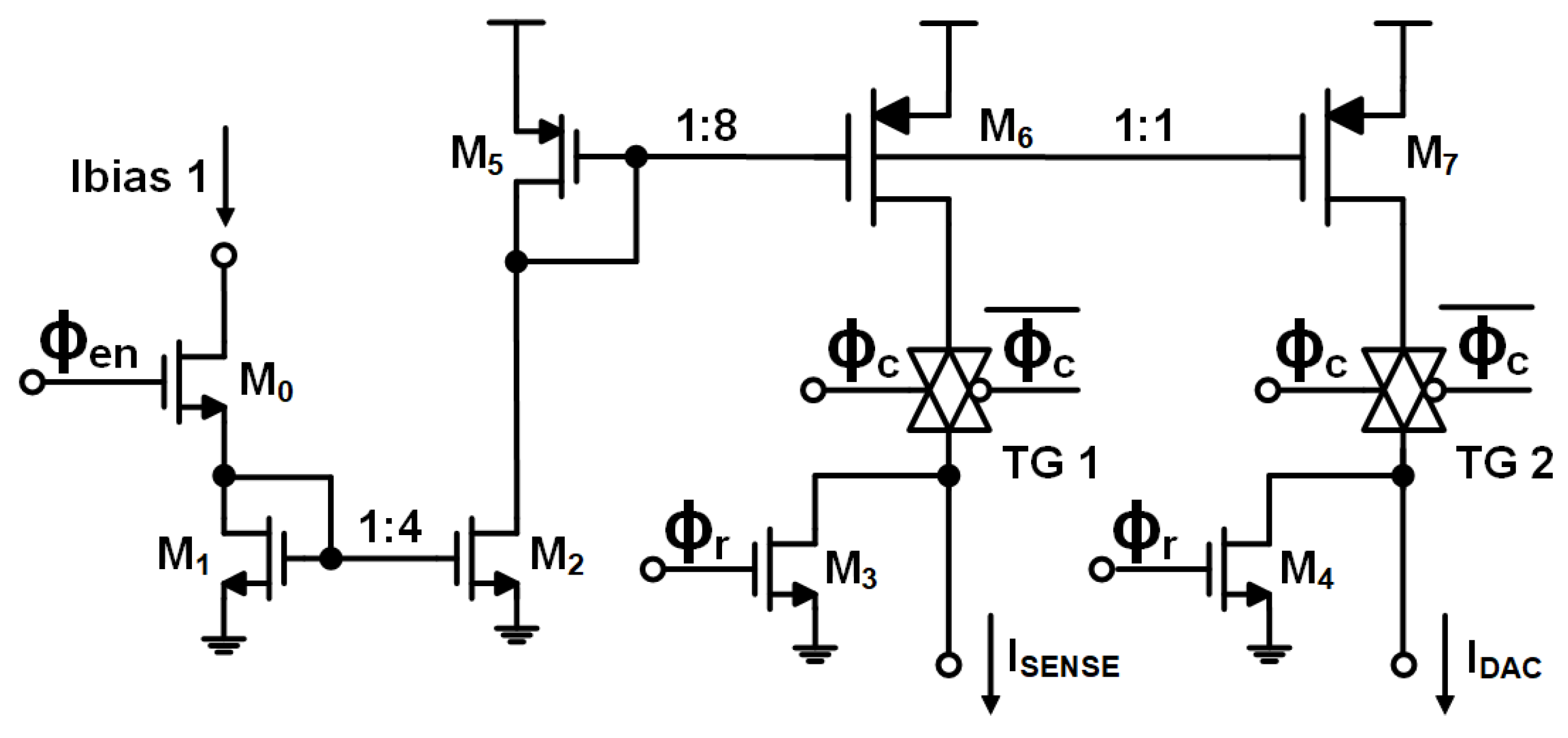
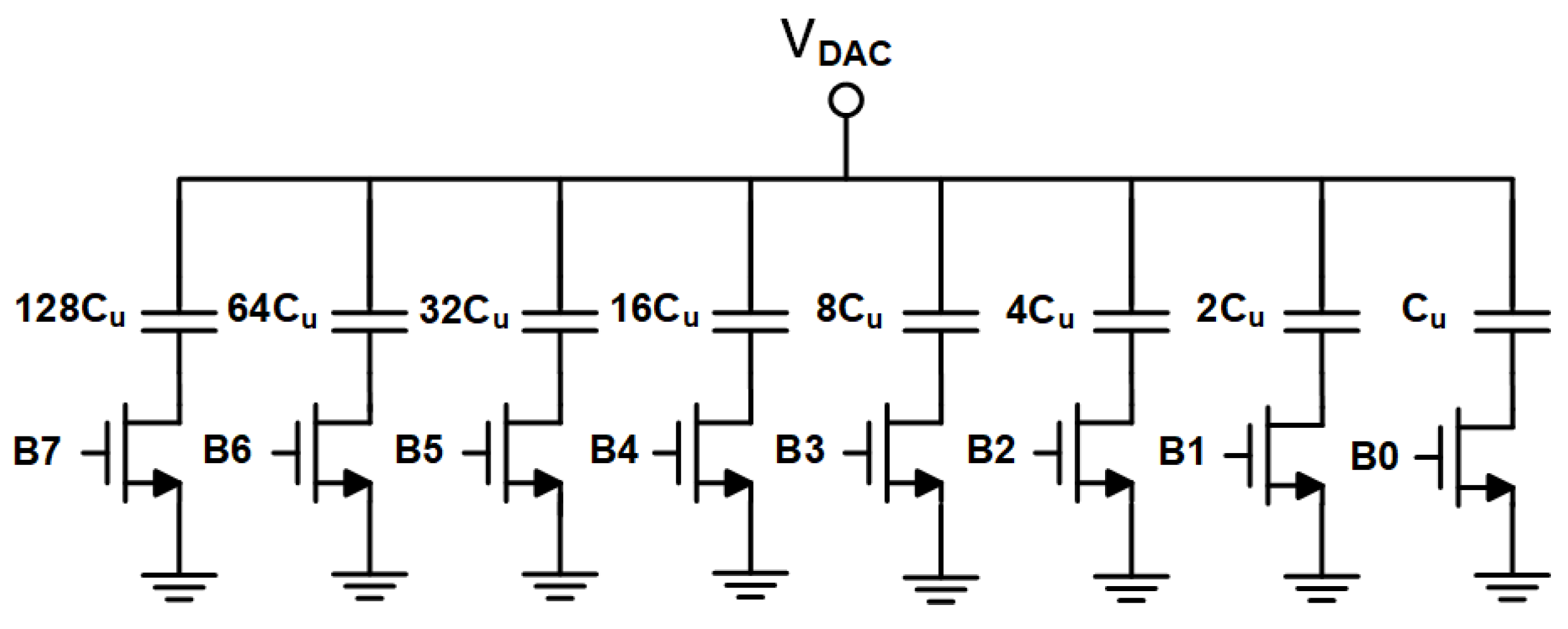
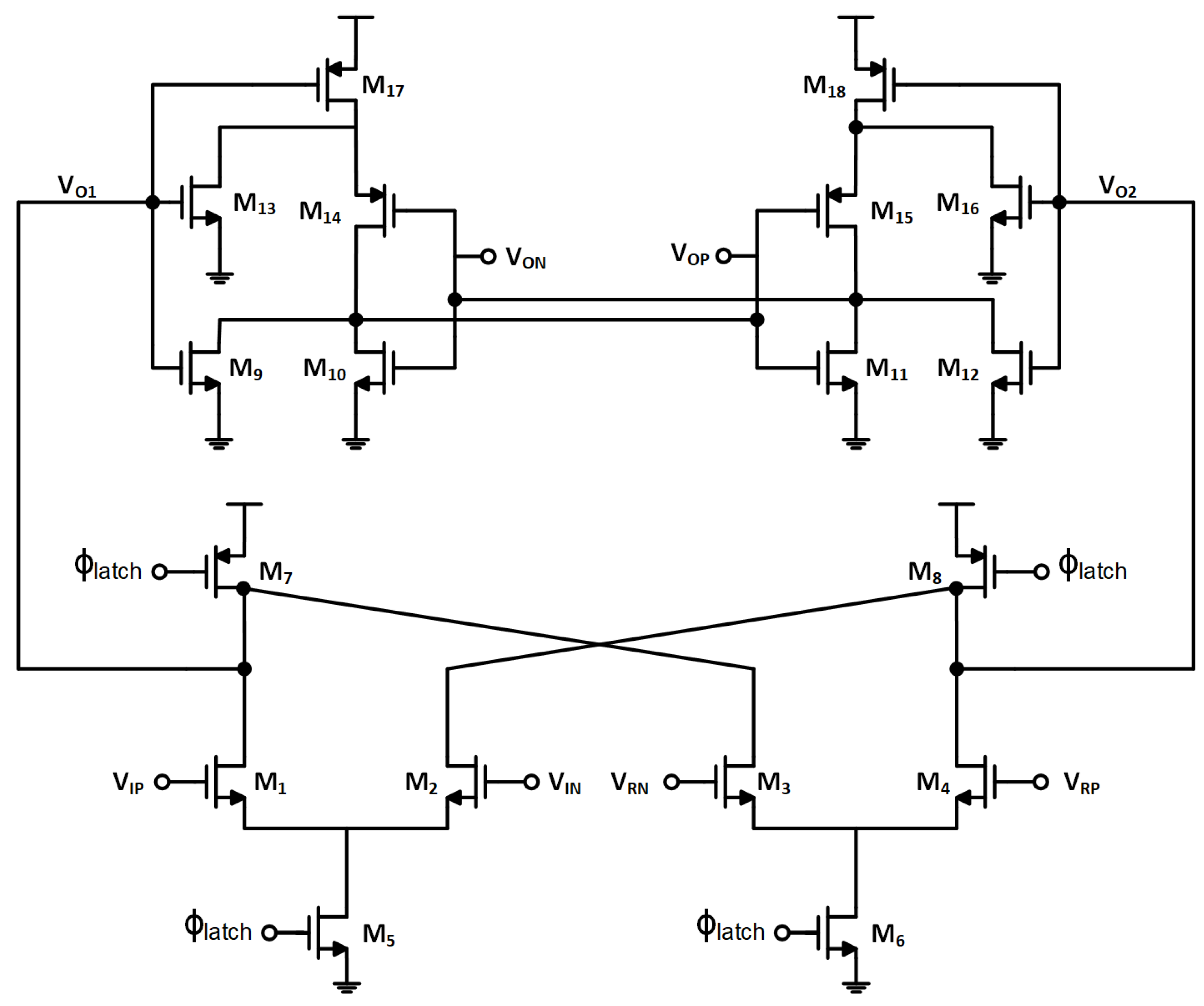
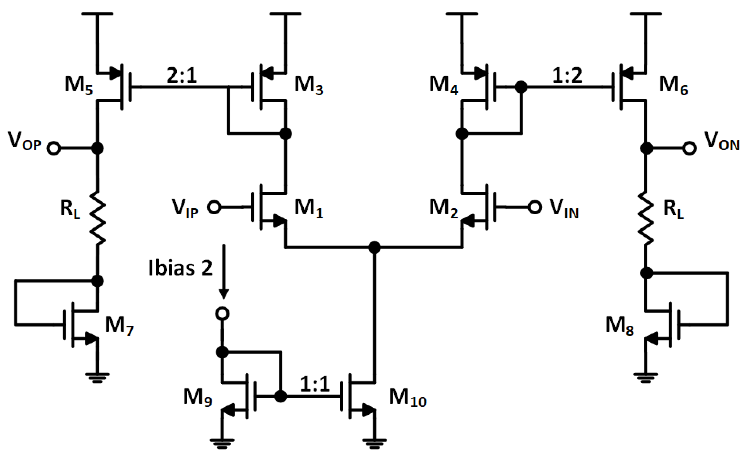
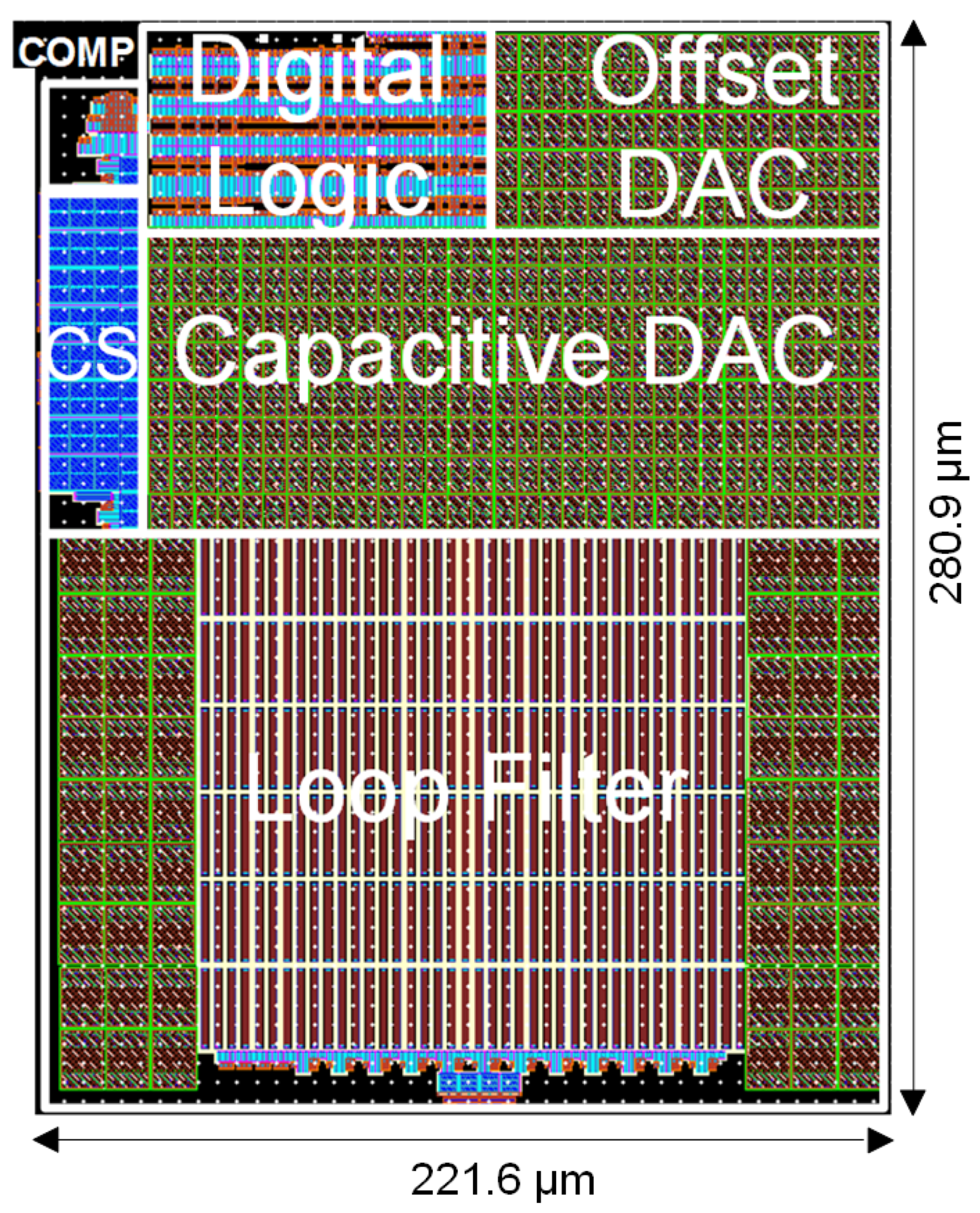
4. Circuit-Level Implementation

In this section, the circuit-level implementation of the proposed CDC is discussed, highlighting some of the circuit details and the trade-offs involved.

4.1. The Charging Current Sources

The circuit diagram of the charging current sources I S E N S E and I D A C is shown in Figure 4. Two current sources are used to generate the charging currents I S E N S E and I D A C . The switch M 0 enables the circuit during the SAR conversion phase, only. Transmission gates are used to implement the switches controlled by ϕ c . I b i a s 1 is equal to 250 nA and is mirrored from M 5 to M 6 and M 7 with a mirroring ratio of value 1:8 to generate the 8.14 μ A charging currents I S E N S E and I D A C . In a practical implementation, I I b i a s 1 is implemented as a programmable current such that the target charging currents values are maintained across process variation. The value of the charging currents is selected such that the maximum value of V s e n s e or V D A C during T C h a r g e , at the minimum input capacitance, remains below V D D V H e a d r o o m , where V H e a d r o o m is the DC voltage headroom of the current sources. It is worth noting that a small charging current results in a small input voltage to the comparator and therefore sets a more strict noise performance on the comparator and hence higher power dissipation. Since the charging current sources directly produce the input voltage to the comparator, the noise contribution of these current sources needs to be considered. The worst-case integrated noise power of each of the charging current sources is given by [11]
V N 2 = 2 3 K T C x o 2 λ v o d
where v o d is the over-drive voltage of the current source transistor and λ is the channel-length modulation constant. Therefore, a relatively large value for V H e a d r o o m is adopted, in the design, to allow a large v o d . A large v o d reduces the noise contribution of the current sources (Equation (5)), and improves the current matching, and hence reduces the gain error (Equation (3)).

4.2. The Capacitive DAC

A regular binary-weighted 8-bit MIM capacitor array is used to implement the CAPDAC (Figure 5). The capacitance matching requirements are set by the differential non-linearity (DNL), and the limit for the minimum C u is determined by
σ D N L = 2 N D A C 2 × σ δ C C u
where σ D N L is the standard deviation of the DNL, and σ δ C C u is the standard deviation of the unit capacitor, which in turn determines the minimum area of C u . The unit capacitance C u is equal to 16.98 fF. The DAC is designed for a maximum DNL less than 0.1 LSB, to avoid quantization noise degradation due to mismatch. The capacitor units in the capacitive DAC are switched on or off using bottom plate switches to avoid the non-linear charge injection error.

4.3. The Multi-Input Comparator and Digital Processing

The multi-input comparator is a dual-differential pair latched comparator [38,41]. The schematic of the comparator is shown in Figure 6. One of the differential pairs is driven by V S E N S E and V D A C , while the other is driven by the differential output of the loop filter. When ϕ l a t c h is high, both the CAPDAC residue voltage and the loop-filter output are sampled, and a differential voltage is created at V o 1 and V o 2 . This differential voltage is applied to the two back-to-back inverters formed by M10, M11, M14, and M15. The back-to-back inverters form a latch producing rail-to-rail digital outputs. When ϕ l a t c h is low, the input to the second stage latch is reset. The comparator is followed by an S-R latch to hold the output. The voltages V D A C and V s e n s e vary by a relatively wide range. Therefore, the effective input common-mode signal to the differential pair varies considerably. Hence, the differential pairs are designed with a large input common-mode range. The smallest voltage that the comparator needs to resolve in this design is 649 μ V , corresponding to the LSB, and the comparator input-referred noise is 430 μ V r m s . This comparator noise is further reduced by the noise-shaping transfer function.
The comparator output is fed to regular SAR logic, followed by a decimation stage. The decimation filter is a third-order cascaded-integrator-comb (CIC) filter. The filter consists of three successive integrator stages formed of adders and unit delays in positive feedback that add the input sample and its unit-delayed version to form the cascaded integrator stage. The next stage is a down-sampler that down-samples the output samples of the cascaded integrator stage by the OSR ratio. Moreover, a comb stage exists after the down-sampler that subtracts the samples from its delayed version in three successive subtraction operations.

4.4. The Loop Filter

The loop filter is formed of two stages. The first stage is a two-tap FIR filter that has two capacitor banks, that is, the C A 1 , 2 capacitor bank and C B 1 , 2 capacitor bank (Figure 1). The FIR filter uses two capacitor banks because each sample of residue voltage contributes to two successive outputs (Equation (2)). The second stage is an inverting switched-capacitor integrator with a feedback capacitor C F , such that α 1 = C A 1 , 2 / C F and α 2 = C B 1 , 2 / C F . Since the residue-sampling switches handle a large input range of V S E N S E and V D A C , they are implemented as CMOS transmission gates. A low-gain two-stage amplifier is used for the second-stage integrator amplifier as shown in Figure 7. The bias current I b i a s 2 is 50 nA. For a well-defined output common mode, the second-stage load is resistive with a diode-connected device to generate a common-mode of value 400 mV, which is half the supply voltage V D D .

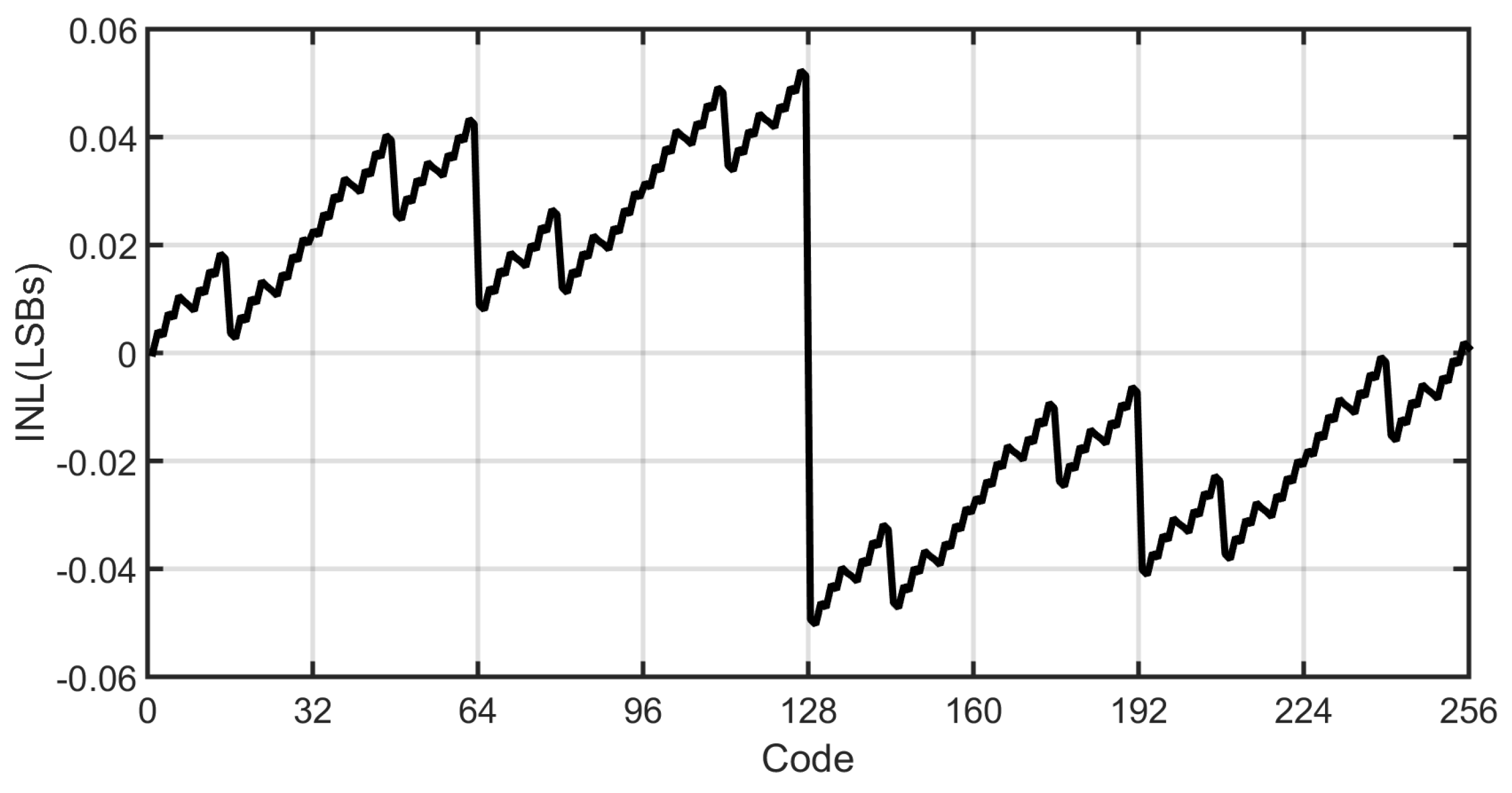
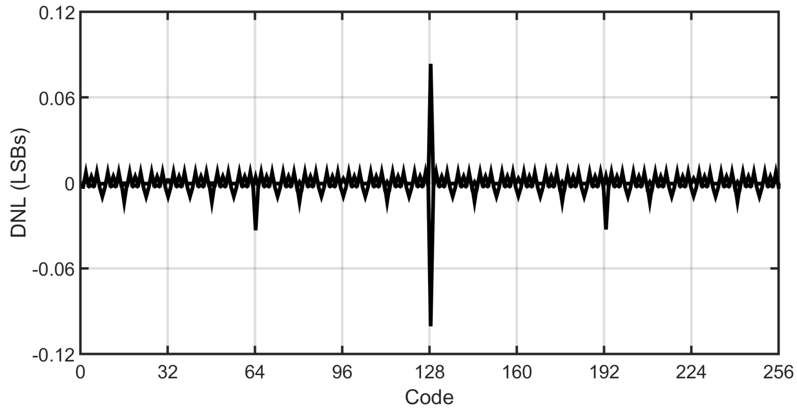
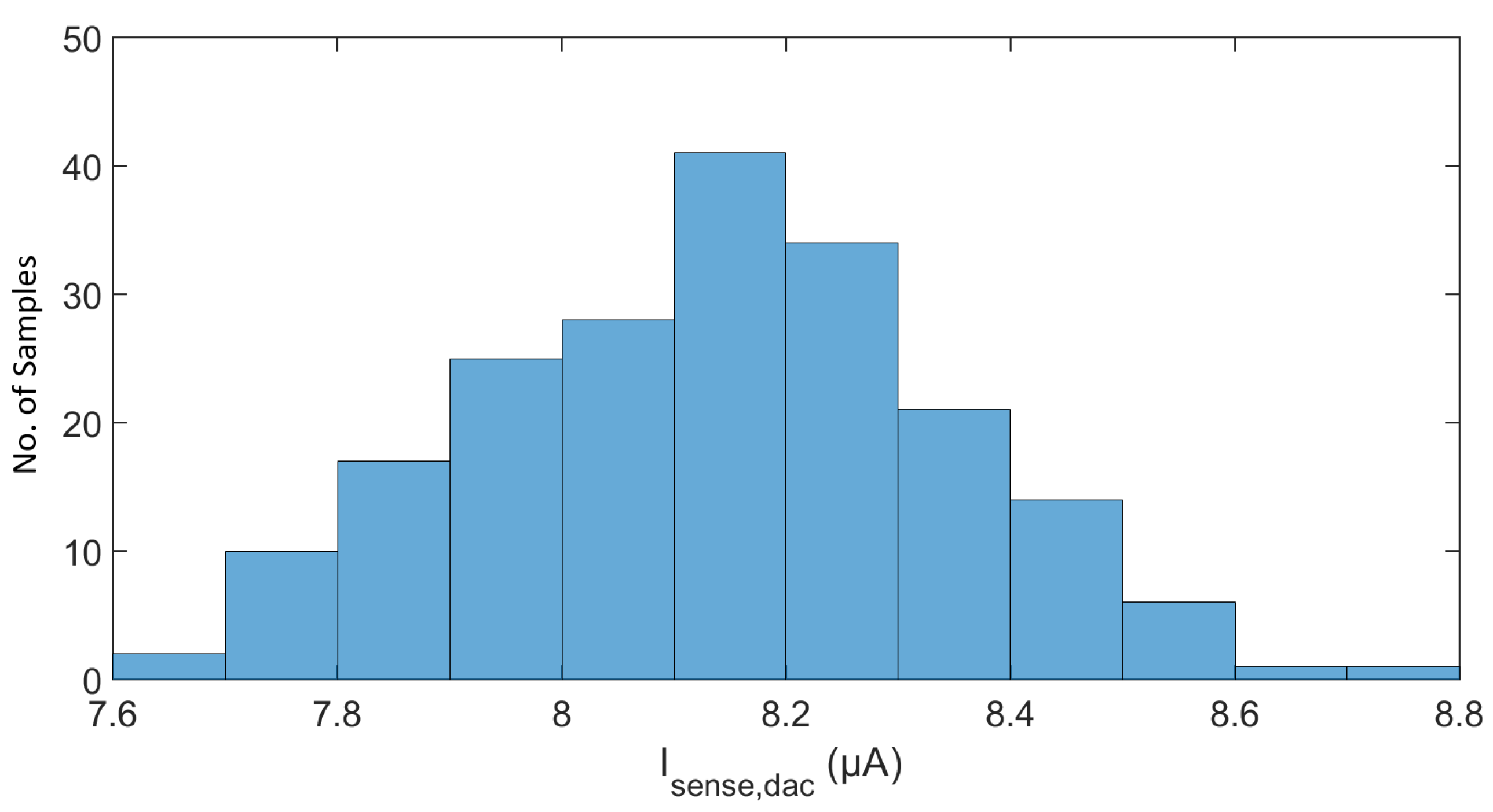
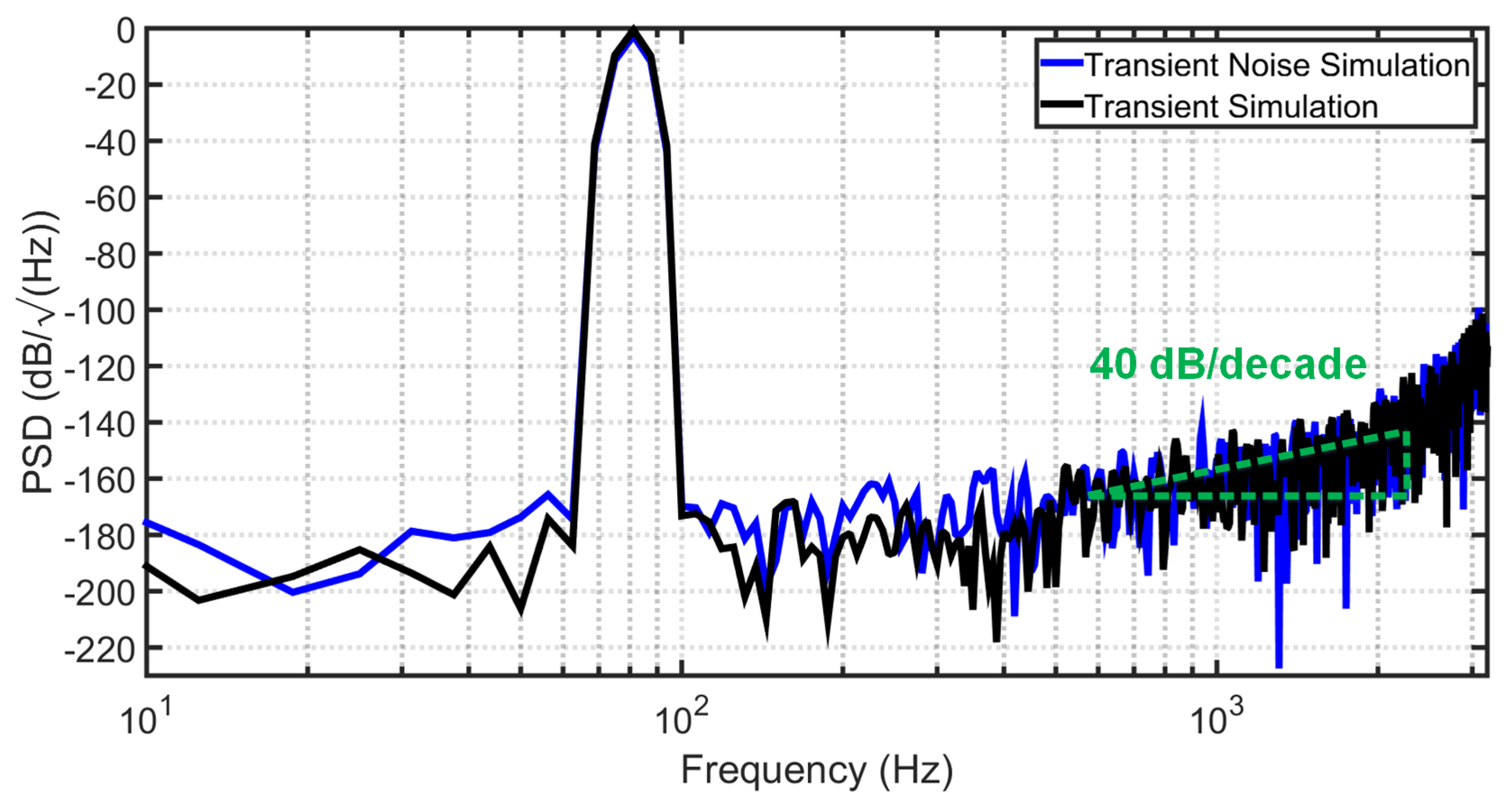
5. Simulation Results

The proposed system is designed towards a 13-bits of resolution for a capacitance range of 4 pF. The circuits are implemented for T c o n v equal to 6 μ s, and T c h a r g e of 305 ns, and at a sampling frequency f s of 6.4 KHz (sampling period ( T s ) of 156.25 μ s). Therefore, this leaves 150.25 μ s for the loop-filter phases. This long time interval relaxes the settling time of the loop filter, and thus its power consumption is also relaxed improving the energy efficiency of the interface. The input signal bandwidth is 200 Hz. That is, the OSR is 16. A higher OSR is avoided, since, in general, a low OSR is recommended for NS SAR for better efficiency [42]. The CDC circuitry is implemented in 130 nm CMOS technology. The layout of the proposed system is shown in Figure 8. The design occupies an area of 0.062 mm2.
Detailed simulations are conducted for different blocks of the proposed architecture and for the overall system. The CAPDAC mismatch is simulated using Monte Carlo simulations, and the worst-case INL and DNL plots are shown in Figure 9 and Figure 10, respectively, indicating max INL and max DNL less than 0.1 LSB. For the charging current sources, the worst-case mismatch is simulated with 200 Monte Carlo runs. The mismatch plot of I S E N S E / I D A C is shown in Figure 11. The standard deviation 1 − σ of the current sources mismatch is found to be equal to 207.5 nA, which is 2.5% for a mean value of 8.14 μ A.
The dynamic performance of the CDC is evaluated with transient noise simulations. The spectrum of the output is shown in Figure 12 for 1024 FFT points at an input signal frequency of 53.125 Hz. The resulting spectrum takes into account the quantization noise, flicker and thermal noise, and the non-linearity errors due to the CAPDAC settling and the absence of the sample-and-hold circuit. The system achieves a signal-to-noise-plus-distortion ratio (SNDR) of 74.0 dB. It is worth noting that the transient simulation without circuit noise achieves an SNDR of 78.8 dB. This means that circuit noise results in a 4.8 dB (0.8 bit) drop in the resolution.
The proposed CDC consumes 1.0 μ A from a supply voltage of 0.8 V. The breakdown of current consumption is tabulated in Table 1. Note that the charging current sources are switched on for a time that is less than 2 % of the sampling period; therefore, a low average current is maintained. The same is true for the rest of circuits that are enabled only when needed.
Different performance metrics of the proposed system are compared to the state-of-the-art published works in Table 2. The FoM used in the table is Walden’s FoM, given by [35,36]
F o M = P o w e r × T m e a s u r e m e n t 2 E N O B
where T m e a s u r e m e n t is the measurement time, defined as ( T s × OSR). T m e a s u r e m e n t is equal to 2500 μ s in this work. The table lists CDCs representing three different architectures: the SAR-based, the Δ Σ , and the NS SAR. The Δ Σ has the highest FoM, indicating the architecture with the lowest energy efficiency. On the other hand, the SAR-based architectures are the most efficient. The proposed CDC of this work has a higher FoM than the other NS SAR implementations of [35,36], but it has a much lower area compared to the other NS SAR and all other architectures. This is attributed to the simplicity of the direct-comparison architecture, but more importantly to the utilization of NS that allows the use of a lower resolution and hence a much smaller 8-bit DAC, rather than a 13-bit CAPDAC to meet the target resolution. Therefore, overall, the proposed architecture has several advantages compared to the other architecture in the table. First, the proposed architecture can interface to a wide range of sensor capacitance, by simply implementing programmability in the charging currents. Other architectures can only interface to a fixed pre-set and designed for sensor capacitance. Second, the proposed architecture does not need an accurate reference voltage, which further adds to the architecture simplicity. Third, the architecture is inherently simple and does not need many blocks. Furthermore, employing NS allows a significant reduction in the Si-area, and hence, providing a low-cost solution, which can be crucial to some applications.
Finally, it should be noted that the reported results of this work are based on detailed transient noise simulations, rather than measurements, as is the case for the other work in the table. However, the main objective of the comparison is to show how the performance of the proposed architecture can fit with respect to the other reported architectures.

6. Conclusions

In this work, a CDC architecture is proposed, where NS is introduced to the SAR-based direct-comparison technique. The direct-comparison technique provides a simple capacitance conversion technique that can interface to a wide range of sensor capacitances by scaling the charging current sources relative to each other. Furthermore, it does not need an accurate voltage reference. The application of NS to this technique allows using a small low-resolution DAC to meet the higher target capacitance-to-digital-conversion resolution. This results in a significant reduction in area. In this implementation, an 8-bit DAC is used to target a 13-bit resolution, using a second-order FIR-IIR filter network in a feed-forward structure with an OSR of 16. The CDC is realized in 130 nm CMOS technology with an area of 0.062 mm2 and achieves an SNDR of 74 dB with a measurement time of 2.5 ms. The CDC consumes 0.8 μ W. resulting in an FoM of 488 fJ/conversion-step.

Author Contributions

Conceptualization, A.H.I.; Methodology, A.F.A.; Validation, A.F.A.; Formal analysis, A.H.I.; Writing—original draft, A.F.A.; Writing—review & editing, A.H.I.; Supervision, H.A.O. and A.H.I. All authors have read and agreed to the published version of the manuscript.

Funding

This research received no external funding.

Data Availability Statement

Simulation results and scripts are archived on the machines of the integrated circuits lab, ECE Dept, Faculty of Engineering, Ain Shams University, Cairo, Egypt.

Conflicts of Interest

The author declares no conflicts of interest.

Abbreviations

The following abbreviations are used in this manuscript:
NSNoise shaping
ADCAnalog-to-Digital converter
DACDigital-to-Analog converter
SARSuccessive-approximation register
CDCCapacitance-to-Digital converter
TDCTime-to-Digital converter
FIRFinite impulse response
IIRInfinite impulse response
OSROversampling ratio
FoMFigure of Merit
NTFNoise transfer function
CIFFCascaded-integrator feed-forward
EFError-feedback
SQNRSignal-to-quantization-noise ratio
SNDRSignal-to-noise and distortion ratio
CAPDACCapacitive DAC
INLIntegral non-linearity
DNLDifferential non-linearity
LSBLeast significant bit
ENOBEffective number of bits

References

  1. Pan, S.; Zhang, X.; Zheng, B.; Cheng, Y.; Jiang, H.; Wu, H. 28.4 A 143dB-Dynamic-Range 119dB-CMRR Capacitance-to-Digital Converter for High-Resolution Floating-Target Displacement Sensing. In Proceedings of the 2025 IEEE International Solid-State Circuits Conference (ISSCC), San Francisco, CA, USA, 16–20 February 2025; Volume 68, pp. 1–3. [Google Scholar] [CrossRef]
  2. Kim, M.; Han, S.; Kim, S.; Rhee, J. A 105 dB Effective Dynamic Range Self- Capacitance Proximity Sensing System with Consecutive Double-Sided Conversion Technique. IEEE Sens. J. 2023, 23, 18325–18337. [Google Scholar] [CrossRef]
  3. Jiang, H.; Amani, S.; Vogel, J.G.; Shalmany, S.H.; Nihtianov, S. A 117-dB In-Band CMRR 98.5-dB SNR Capacitance-to-Digital Converter for Sub-nm Displacement Sensing with an Electrically Floating Target. IEEE Solid-State Circuits Lett. 2020, 3, 9–12. [Google Scholar] [CrossRef]
  4. Xia, S.; Makinwa, K.; Nihtianov, S. A capacitance-to-digital converter for displacement sensing with 17b resolution and 20μs conversion time. In Proceedings of the 2012 IEEE International Solid-State Circuits Conference, San Francisco, CA, USA, 19–23 February 2012; pp. 198–200. [Google Scholar] [CrossRef]
  5. Xia, Q.; Zhou, F.; Niu, Y.; He, M.; Lu, W.; Zhang, Y.; Chen, Z. An Energy-Efficient Capacitance-to-Digital Converter with Top and Bottom Plate Sampling for Pressure Sensors. IEEE Trans. Circuits Syst. II Express Briefs 2025. early access. [Google Scholar] [CrossRef]
  6. Keshyagol, K.; Hiremath, S.; H. M., V.; Kini U., A.; Naik, N.; Hiremath, P. Optimizing Capacitive Pressure Sensor Geometry: A Design of Experiments Approach with a Computer-Generated Model. Sensors 2024, 24, 3504. [Google Scholar] [CrossRef]
  7. Xia, Q.J.; Zhang, Y.C.; You, Y.; Zhou, F.; Lu, W.g. A 9.1μW Capacitance-to-Digital Converter for Pressure Sensor Systems. In Proceedings of the 2022 IEEE 16th International Conference on Solid-State & Integrated Circuit Technology (ICSICT), Nangjing, China, 25–28 October 2022; pp. 1–3. [Google Scholar] [CrossRef]
  8. Park, S.; Lee, G.H.; Cho, S. A 2.92-μW Capacitance-to-Digital Converter With Differential Bondwire Accelerometer, On-Chip Air Pressure, and Humidity Sensor in 0.18-μm CMOS. IEEE J. Solid-State Circuits 2019, 54, 2845–2856. [Google Scholar] [CrossRef]
  9. Kar, S.; Leon-Salas, W.D. A low-power 12-bit capacitance-to-digital converter for capacitive MEMS pressure sensor. In Proceedings of the SENSORS, Limerick, Ireland, 28–31 October 2011; pp. 1855–1858. [Google Scholar] [CrossRef]
  10. Ismail, A.; El-Nafarawi, M. Energy-efficient successive-approximation-register based capacitive interface for pressure sensors. Electron. Lett. 2015, 51, 2007–2009. [Google Scholar] [CrossRef]
  11. Ismail, A.H.; El-Nafarawi, M. A low-energy SAR-based capacitance-to-digital converter for pressure sensors: System analysis, design and calibration. In Proceedings of the 2016 IEEE 59th International Midwest Symposium on Circuits and Systems (MWSCAS), Abu Dhabi, United Arab Emirates, 16–19 October 2016; pp. 1–4. [Google Scholar] [CrossRef]
  12. Wei, Y.; Zheng, H.; Liu, X. A wide dynamic range, high-resolution multi-step SAR CDC for implanted humidity sensors. In Proceedings of the 2024 IEEE Biomedical Circuits and Systems Conference (BioCAS), Xi’an, China, 24–26 October 2024; pp. 1–5. [Google Scholar] [CrossRef]
  13. Li, H.; Tan, Z.; Bao, Y.; Xiao, H.; Zhang, H.; Du, K.; Shen, L.; Ru, J.; Zhang, Y.; Ye, L.; et al. Energy-Efficient CMOS Humidity Sensors Using Adaptive Range-Shift Zoom CDC and Power-Aware Floating Inverter Amplifier Array. IEEE J. Solid-State Circuits 2021, 56, 3560–3572. [Google Scholar] [CrossRef]
  14. Wen, Y.; Demosthenous, A.; Donaldson, N.; Liu, X. A Capacitance-to-Digits Readout Circuit for Integrated Humidity Sensors for Monitoring the In-Package Humidity of Ultra-Small Medical Implants. In Proceedings of the 2018 IEEE International Symposium on Circuits and Systems (ISCAS), Florence, Italy, 27–30 May 2018; pp. 1–4. [Google Scholar] [CrossRef]
  15. Lai, K.Y.T.; Yang, Y.T.; Chen, B.J.; Shen, C.J.; Shiu, M.F.; He, Z.C.; Chang, H.C.; Lee, C.Y. A 3.3V 15.6b 6.1pJ/0.02%RH with 10ms response humidity sensor for respiratory monitoring. In Proceedings of the 2014 IEEE Asian Solid-State Circuits Conference (A-SSCC), KaoHsiung, Taiwa, 10–12 November 2014; pp. 293–296. [Google Scholar] [CrossRef]
  16. Tan, Z.; Daamen, R.; Humbert, A.; Ponomarev, Y.V.; Chae, Y.; Pertijs, M.A.P. A 1.2-V 8.3-nJ CMOS Humidity Sensor for RFID Applications. IEEE J. Solid-State Circuits 2013, 48, 2469–2477. [Google Scholar] [CrossRef]
  17. Long, S.; Ma, S.; Fan, X.; Wu, C.; Tong, Z.; He, K.; Tang, X. An ASIC Interface for MEMS Vibratory Gyroscopes with a 110 dB DR and 0.001 s/Hz Noise Floor over a 100 Hz. In Proceedings of the 2023 8th International Conference on Integrated Circuits and Microsystems (ICICM), Nanjing, China, 20–23 October 2023; pp. 55–60. [Google Scholar] [CrossRef]
  18. Jiang, H.; Liu, Y.; Middelburg, L.; Mansouri, B.E.; Nihtianov, S. A Continuous-Time Readout IC with 0.12 aF/Hz for Capacitive Inertial Sensors. In Proceedings of the 2021 IEEE International Conference on Integrated Circuits, Technologies and Applications (ICTA), Zhuhai, China, 24–26 November 2021; pp. 14–15. [Google Scholar] [CrossRef]
  19. Rombach, S.; Marx, M.; Nessler, S.; De Dorigo, D.; Maurer, M.; Manoli, Y. An Interface ASIC for MEMS Vibratory Gyroscopes with a Power of 1.6 mW, 92 dB DR and 0.007°/s/Hz Noise Floor over a 40 Hz Band. IEEE J. Solid-State Circuits 2016, 51, 1915–1927. [Google Scholar] [CrossRef]
  20. Tan, Z.; Nguyen, K.; Yan, J.; Samuels, H.; Keating, S.; Crocker, P.; Clark, B. A dual-axis MEMS vibratory gyroscope ASIC with 0.0061°/s/VHz noise floor over 480 Hz bandwidth. In Proceedings of the 2017 IEEE Asian Solid-State Circuits Conference (A-SSCC), Seoul, Republic of Korea, 6–8 November 2017; pp. 21–24. [Google Scholar] [CrossRef]
  21. Ezekwe, C.D.; Boser, B.E. A Mode-Matching ΣΔ Closed-Loop Vibratory Gyroscope Readout Interface With a 0.004°/s/Hz Noise Floor Over a 50 Hz Band. IEEE J. Solid-State Circuits 2008, 43, 3039–3048. [Google Scholar] [CrossRef]
  22. Ghanbari, M.M.; Tsai, J.M.; Gambini, S. An energy-efficient heterogeneously-integrated capacitive pressure sensing system. In Proceedings of the 2015 IEEE Biomedical Circuits and Systems Conference (BioCAS), Atlanta, GA, USA, 22–24 October 2015; pp. 1–4. [Google Scholar] [CrossRef]
  23. Trung, N.T.; Häfliger, P. A Submicrowatt Implantable Capacitive Sensor System for Biomedical Applications. IEEE Trans. Circuits Syst. II Express Briefs 2015, 62, 209–213. [Google Scholar] [CrossRef]
  24. Shin, D.Y.; Lee, H.; Kim, S. A Delta–Sigma Interface Circuit for Capacitive Sensors with an Automatically Calibrated Zero Point. IEEE Trans. Circuits Syst. II Express Briefs 2011, 58, 90–94. [Google Scholar] [CrossRef]
  25. Jung, Y.; Duan, Q.; Roh, J. A 17.4-b Delta-Sigma Capacitance-to-Digital Converter for One-Terminal Capacitive Sensors. IEEE Trans. Circuits Syst. II Express Briefs 2017, 64, 1122–1126. [Google Scholar] [CrossRef]
  26. Omran, H.; Alhoshany, A.; Alahmadi, H.; Salama, K.N. A 33fJ/Step SAR Capacitance-to-Digital Converter Using a Chain of Inverter-Based Amplifiers. IEEE Trans. Circuits Syst. I Regul. Pap. 2017, 64, 310–321. [Google Scholar] [CrossRef]
  27. Alhoshany, A.; Omran, H.; Salama, K.N. A 45.8fJ/Step, energy-efficient, differential SAR capacitance-to-digital converter for capacitive pressure sensing. Sens. Actuators A Phys. 2016, 245, 10–18. [Google Scholar] [CrossRef]
  28. Jiang, H.; Wang, Z.; Liu, L.; Zhang, C.; Wang, Z. A combined low power SAR capacitance-to-digital / analog-to-digital converter for multisensory system. In Proceedings of the 2012 IEEE 55th International Midwest Symposium on Circuits and Systems (MWSCAS), Boise, ID, USA, 5–8 August 2012; pp. 1000–1003. [Google Scholar] [CrossRef]
  29. Oh, S.; Lee, Y.; Wang, J.; Foo, Z.; Kim, Y.; Jung, W.; Li, Z.; Blaauw, D.; Sylvester, D. A Dual-Slope Capacitance-to-Digital Converter Integrated in an Implantable Pressure-Sensing System. IEEE J. Solid-State Circuits 2015, 50, 1581–1591. [Google Scholar] [CrossRef]
  30. Sanjurjo, J.; Prefasi, E.; Buffa, C.; Gaggl, R. An energy-efficient 17-bit noise-shaping Dual-Slope Capacitance-to-Digital Converter for MEMS sensors. In Proceedings of the ESSCIRC Conference 2016: 42nd European Solid-State Circuits Conference, Lausanne, Switzerland, 12–15 September 2016; pp. 389–392. [Google Scholar] [CrossRef]
  31. Rogi, C.; Buffa, C.; De Milleri, N.; Gaggl, R.; Prefasi, E. A Fully-Differential Switched-Capacitor Dual-Slope Capacitance-To-Digital Converter (CDC) for a Capacitive Pressure Sensor. Sensors 2019, 19, 3673. [Google Scholar] [CrossRef]
  32. He, Y.; Chang, Z.y.; Pakula, L.; Shalmany, S.H.; Pertijs, M. 27.7 A 0.05 mm2 1V capacitance-to-digital converter based on period modulation. In Proceedings of the 2015 IEEE International Solid-State Circuits Conference - (ISSCC) Digest of Technical Papers, San Francisco, CA, USA, 22–26 February 2015; pp. 1–3. [Google Scholar] [CrossRef]
  33. Hassan, A.H.; Fouad, A.; Mostafa, H.; Salama, K.N.; Soliman, A.M. A New Design Methodology for Time-Based Capacitance-to-Digital Converters (T-CDCs). AEU Int. J. Electron. Commun. 2018, 96, 238–245. [Google Scholar] [CrossRef]
  34. Jung, W.; Jeong, S.; Oh, S.; Sylvester, D.; Blaauw, D. 27.6 A 0.7pF-to-10nF fully digital capacitance-to-digital converter using iterative delay-chain discharge. In Proceedings of the 2015 IEEE International Solid-State Circuits Conference - (ISSCC) Digest of Technical Papers, San Francisco, CA, USA, 22–26 February 2015; pp. 1–3. [Google Scholar] [CrossRef]
  35. Alhoshany, A.; Salama, K.N. A Precision, Energy-Efficient, Oversampling, Noise-Shaping Differential SAR Capacitance-to-Digital Converter. IEEE Trans. Instrum. Meas. 2019, 68, 392–401. [Google Scholar] [CrossRef]
  36. Lim, C.; Choi, Y.; Song, J.; Ahn, S.; Jang, S.; Kim, C. An 88.9-dB SNR Fully-Dynamic Noise-Shaping SAR Capacitance-to-Digital Converter. IEEE J. Solid-State Circuits 2022, 57, 2778–2790. [Google Scholar] [CrossRef]
  37. Jie, L.; Tang, X.; Liu, J.; Shen, L.; Li, S.; Sun, N.; Flynn, M.P. An Overview of Noise-Shaping SAR ADC: From Fundamentals to the Frontier. IEEE Open J. Solid-State Circuits Soc. 2021, 1, 149–161. [Google Scholar] [CrossRef]
  38. Fredenburg, J.A.; Flynn, M.P. A 90-MS/s 11-MHz-Bandwidth 62-dB SNDR Noise-Shaping SAR ADC. IEEE J. Solid-State Circuits 2012, 47, 2898–2904. [Google Scholar] [CrossRef]
  39. Fredenburg, J.; Flynn, M. A 90MS/s 11MHz bandwidth 62dB SNDR noise-shaping SAR ADC. In Proceedings of the 2012 IEEE International Solid-State Circuits Conference, San Francisco, CA, USA, 19–23 February 2012; pp. 468–470. [Google Scholar]
  40. Luo, Y.; Jain, A.; Wagner, J.; Ortmanns, M. Input Referred Comparator Noise in SAR ADCs. IEEE Trans. Circuits Syst. II Express Briefs 2019, 66, 718–722. [Google Scholar] [CrossRef]
  41. Yip, M.; Chandrakasan, A.P. A resolution-reconfigurable 5-to-10b 0.4-to-1V power scalable SAR ADC. In Proceedings of the 2011 IEEE International Solid-State Circuits Conference, San Francisco, CA, USA, 20–24 February 2011; pp. 190–192. [Google Scholar] [CrossRef]
  42. Ismail, A.H. On the System-Level Design of Noise-Shaping SAR Analog-to-Digital Converters. Electronics 2024, 13, 4128. [Google Scholar] [CrossRef]
Figure 1. Block diagram of the proposed NS SAR CDC.
Electronics 14 01386 g001
Figure 2. The NTF.
Figure 2. The NTF.
Electronics 14 01386 g002
Figure 3. Timing diagram of the proposed NS SAR CDC.
Electronics 14 01386 g003
Figure 4. Schematic of the charging current sources.
Electronics 14 01386 g004
Figure 5. The 8-bit capacitive DAC.
Electronics 14 01386 g005
Figure 6. The circuit diagram of the multi-input comparator.
Electronics 14 01386 g006
Figure 7. The circuit diagram of IIR filter Opamp.
Electronics 14 01386 g007
Figure 8. Layout of the proposed system. “CS” is the charging current sources circuitry.
Electronics 14 01386 g008
Figure 9. Worst-case INL.
Electronics 14 01386 g009
Figure 10. Worst-case DNL.
Electronics 14 01386 g010
Figure 11. Charging current sources mismatch.
Electronics 14 01386 g011
Figure 12. Output spectrum of the proposed NS SAR CDC.
Electronics 14 01386 g012
Table 1. Current consumption breakdown of the proposed CDC.
BlockCurrent Consumption (nA)Percentage %
Charging current sources33433.1
Multi-input comparator505
Noise-shaping Filter22522.3
Digital and C D A C switching40039.6
Table 2. Performance summary and comparison.
SpecificationTIM’ 2019JSSC’ 2022ISSCC’ 2012JSNA’ 2016TCAS-I’ 2017This
[35][36][4][27][26]Work *
Technology (nm)180180350180180130
ArchitectureNS SARNS SAR Δ Σ SARSARNS SAR
Noise-Shaping Order1st2nd3rd--2nd
Dynamic RangeFixedFixedFixedFixedFixedScalable
Offset Cap. Cancel.N/AN/AYesN/AN/AYes
Supply Voltage (V)0.8/11.83.30.9/10.8/1.20.8
Input Range (pF)3.613.63.216.1412.664
Meas. Time ( μ S)810502042.5162500
Cap. Resolution ( a F r m s )1501726513001200282
Power Consump. ( μ W)1.5963.2815,0003.846.440.8
Resolution (bits)1112612128
ENOB (bits)12.7414.513.811.811.612.0
SNDR (dB)78.588.984.872.871.674.0
Area (mm2)0.30.252.60.10.20.062
FoM (fJ/conv.-step)18713920,82345.833488
* Simulation results.
Disclaimer/Publisher’s Note: The statements, opinions and data contained in all publications are solely those of the individual author(s) and contributor(s) and not of MDPI and/or the editor(s). MDPI and/or the editor(s) disclaim responsibility for any injury to people or property resulting from any ideas, methods, instructions or products referred to in the content.

