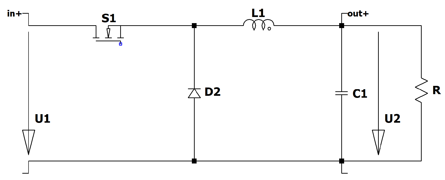
Figure 1.
Circuit diagram of the Buck converter.
Figure 1.
Circuit diagram of the Buck converter.
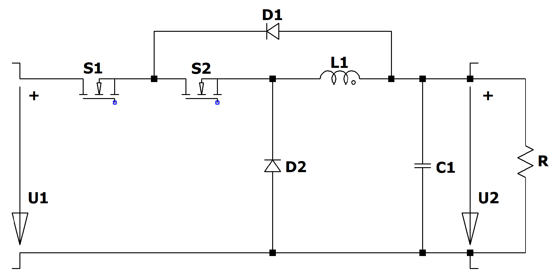
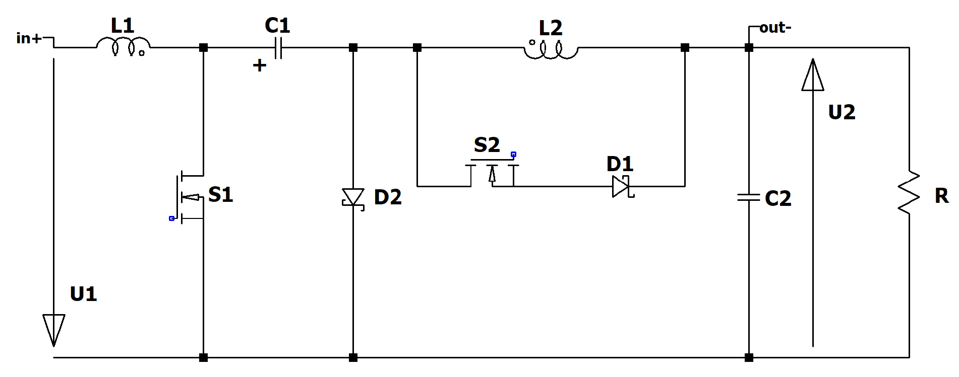
Figure 2.
Circuit diagram of the tristate Buck converter.
Figure 2.
Circuit diagram of the tristate Buck converter.
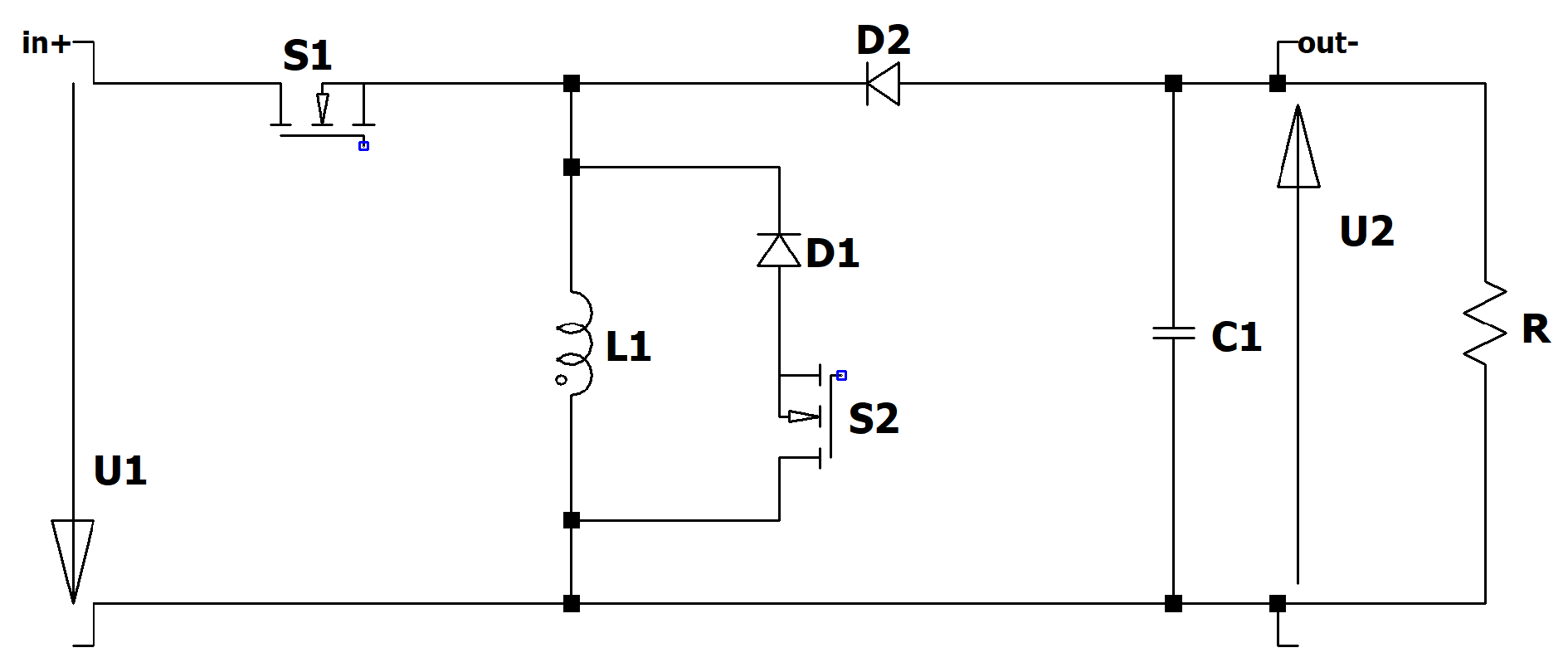
Figure 3.
Circuit diagram of the RLT Buck converter.
Figure 3.
Circuit diagram of the RLT Buck converter.
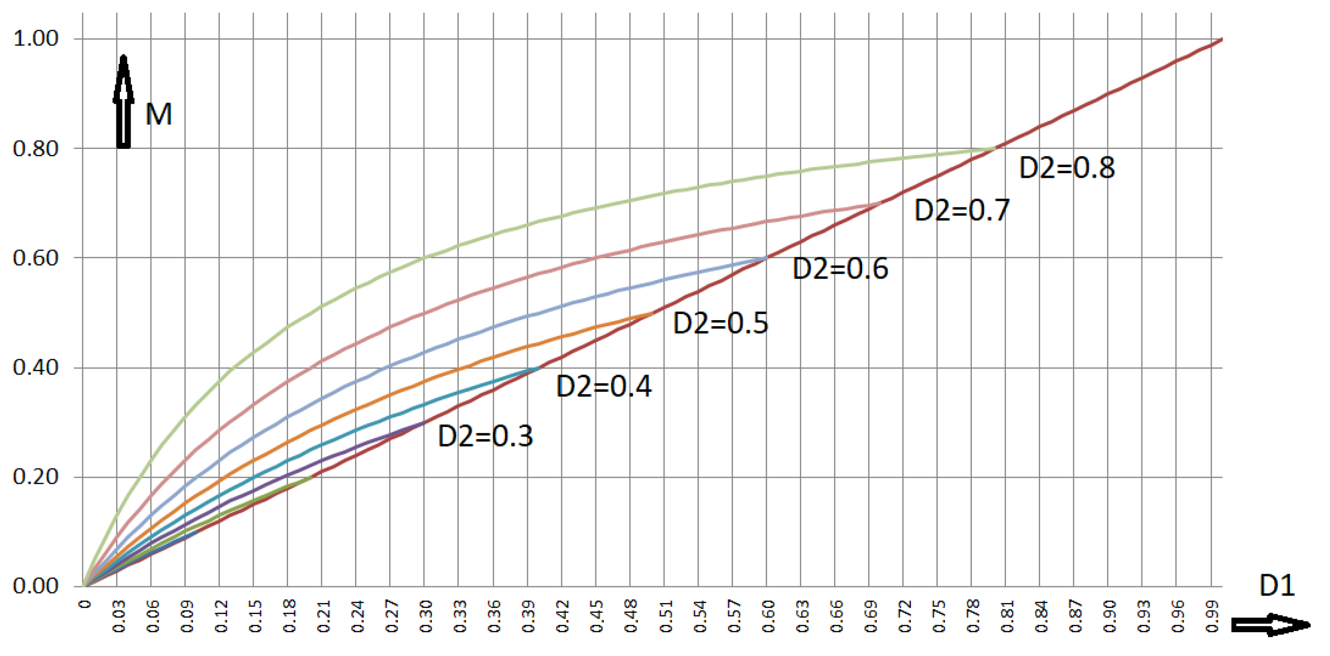
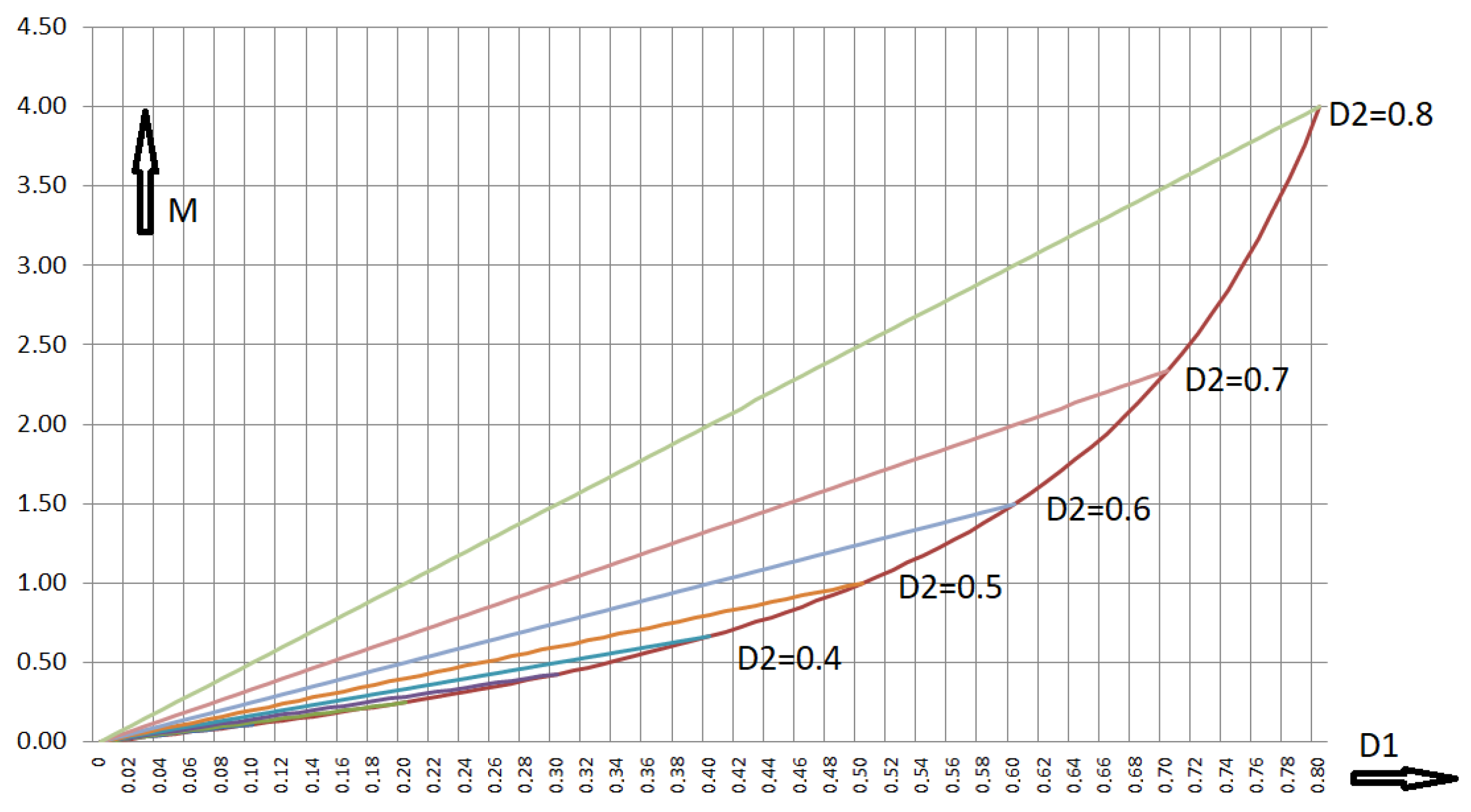
Figure 4.
Voltage transformation ratio of the RLT Buck: duty cycle of switch S2 is kept constant, duty cycle of switch S1 is used as variable.
Figure 4.
Voltage transformation ratio of the RLT Buck: duty cycle of switch S2 is kept constant, duty cycle of switch S1 is used as variable.
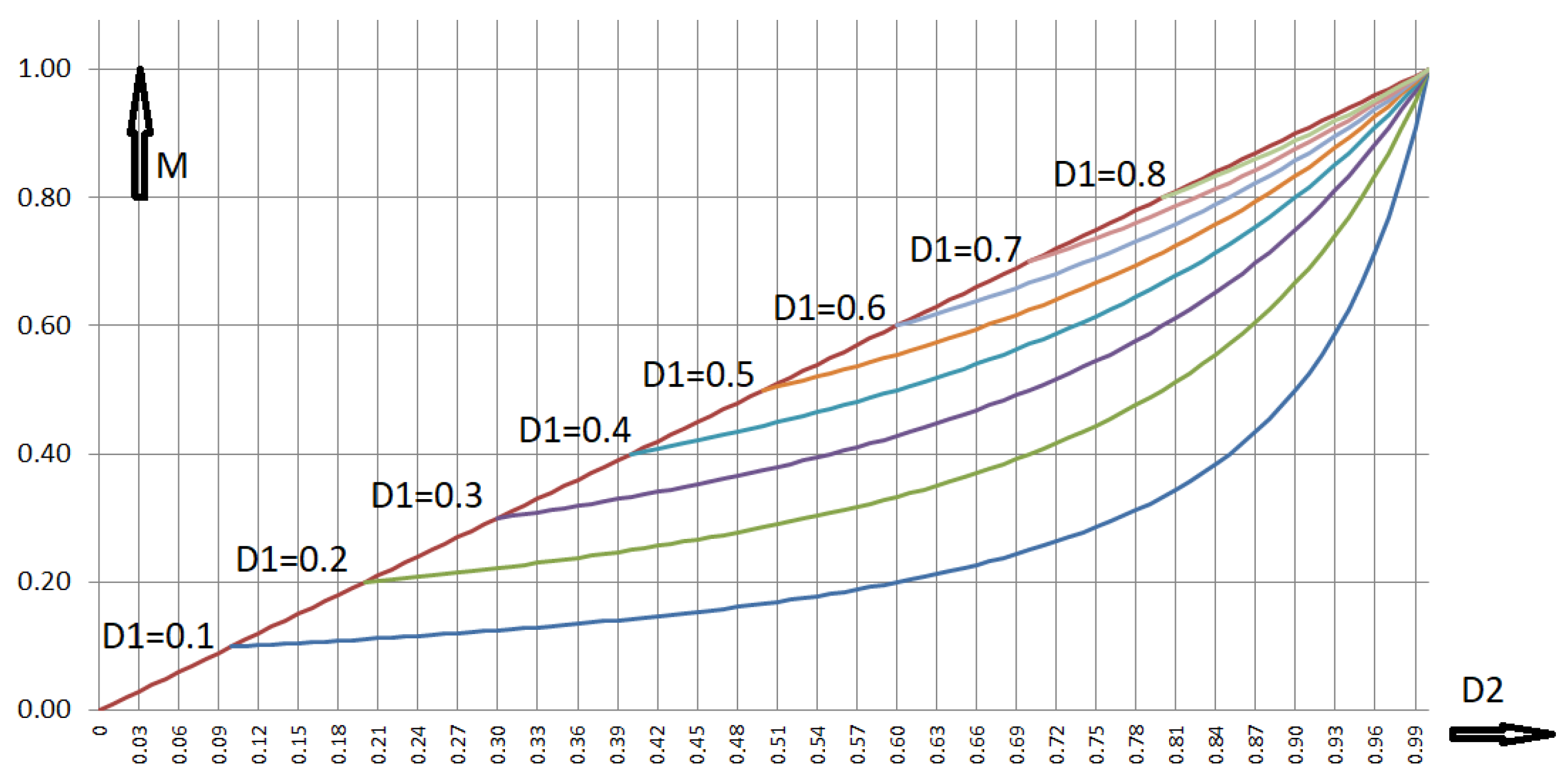
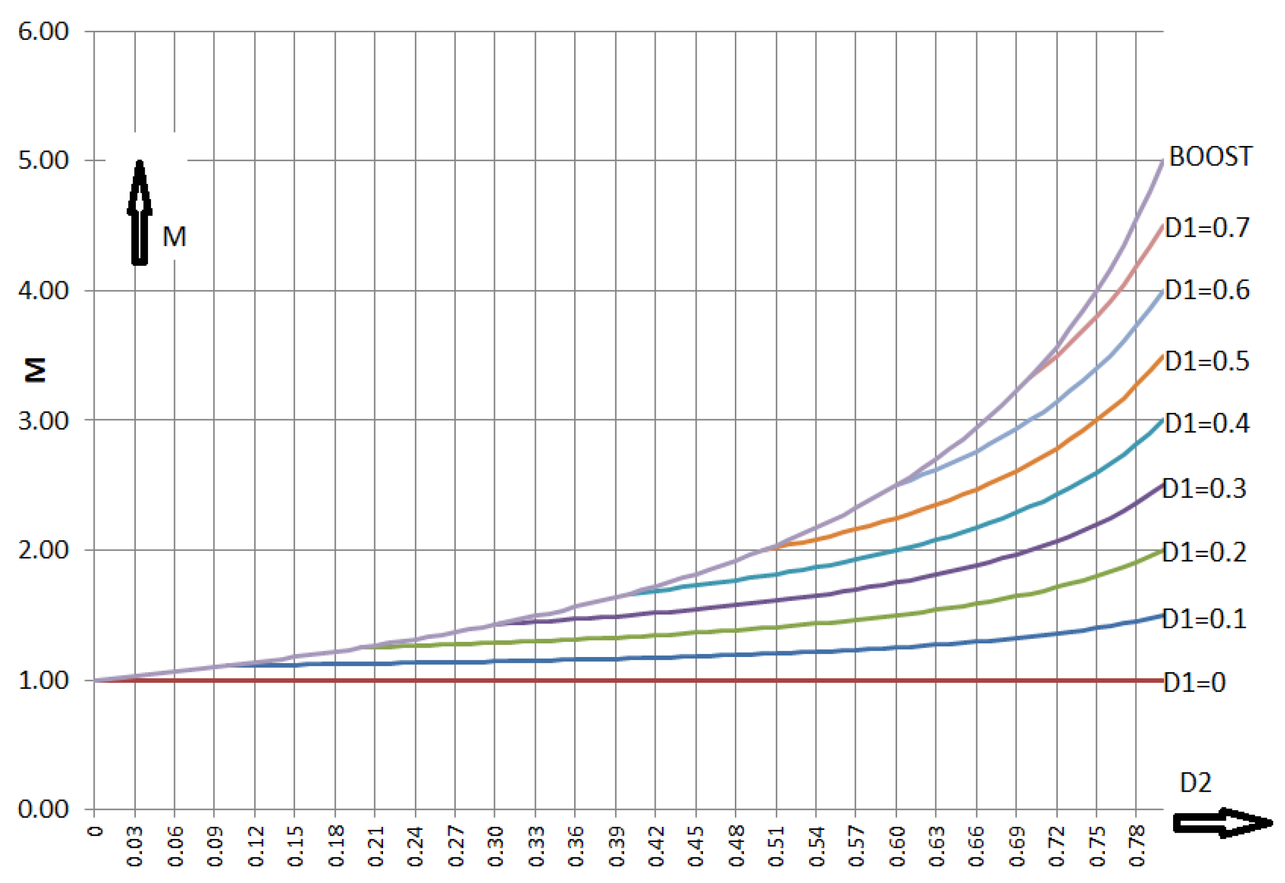
Figure 5.
Voltage transformation ratio of the RLT Buck: duty cycle of switch S1 is kept constant, duty cycle of switch S2 is used as variable.
Figure 5.
Voltage transformation ratio of the RLT Buck: duty cycle of switch S1 is kept constant, duty cycle of switch S2 is used as variable.
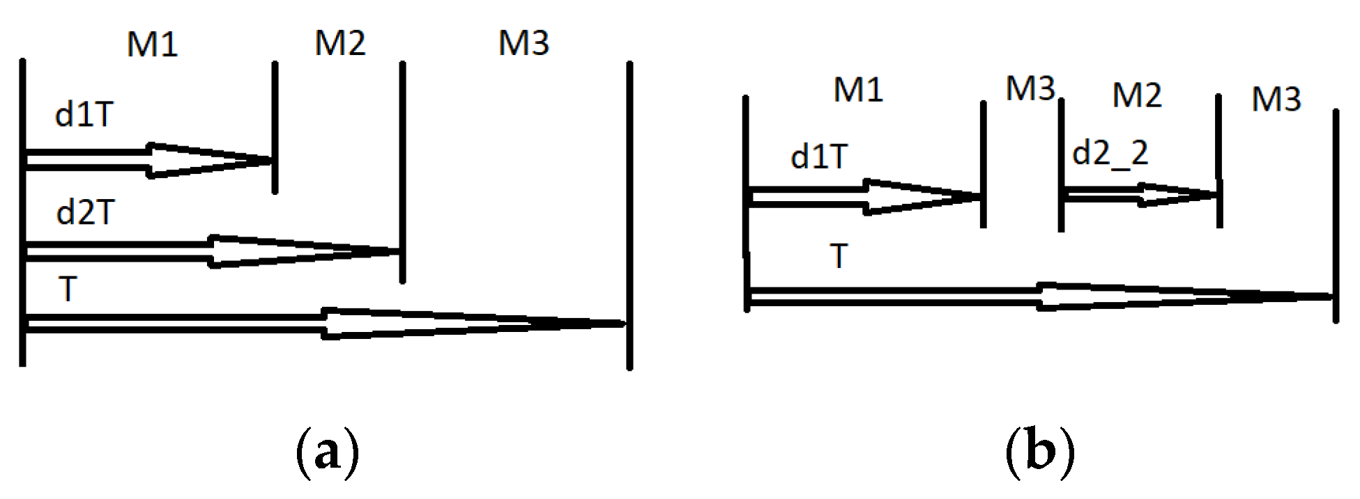
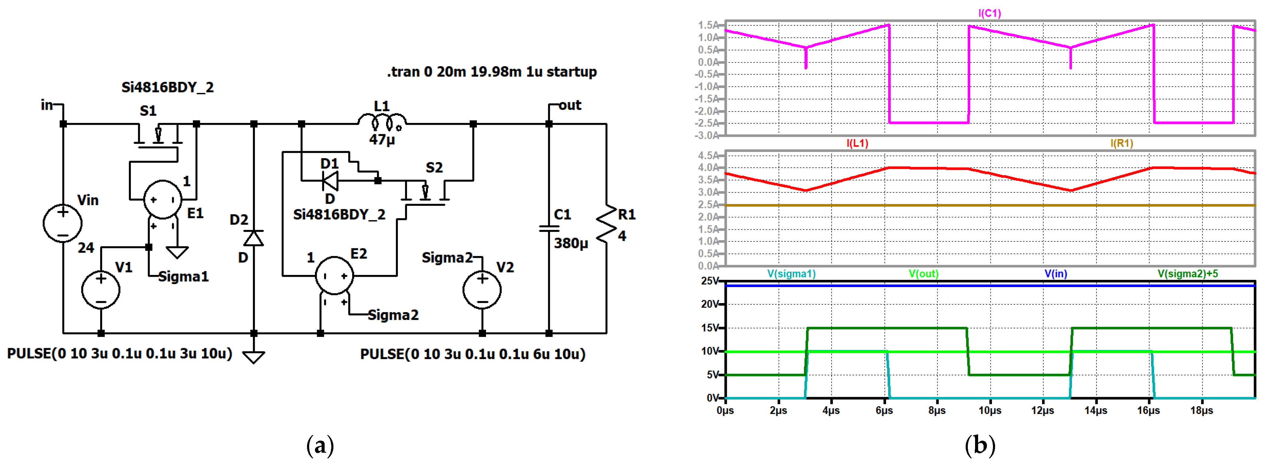
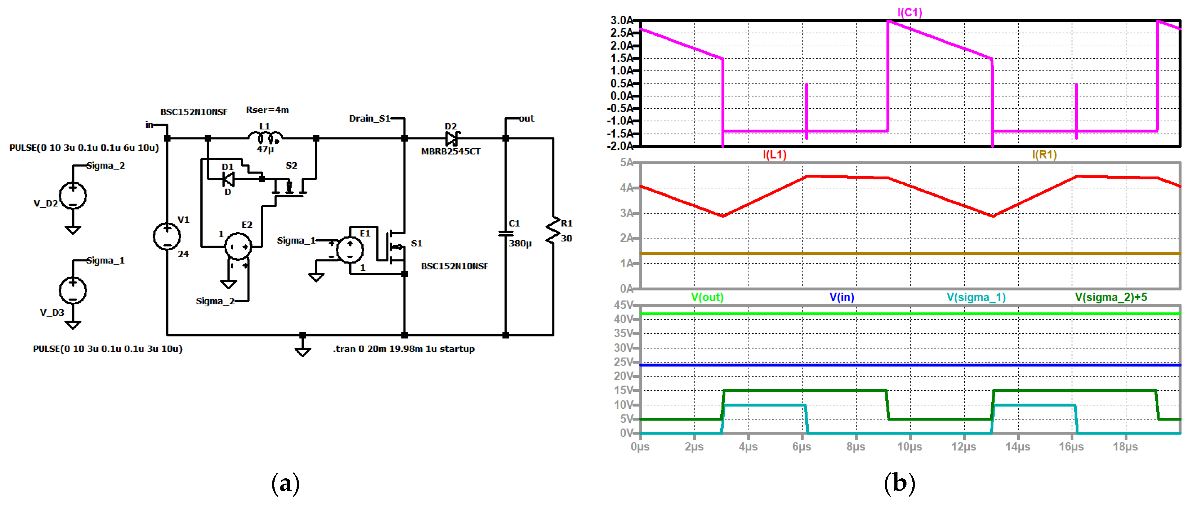
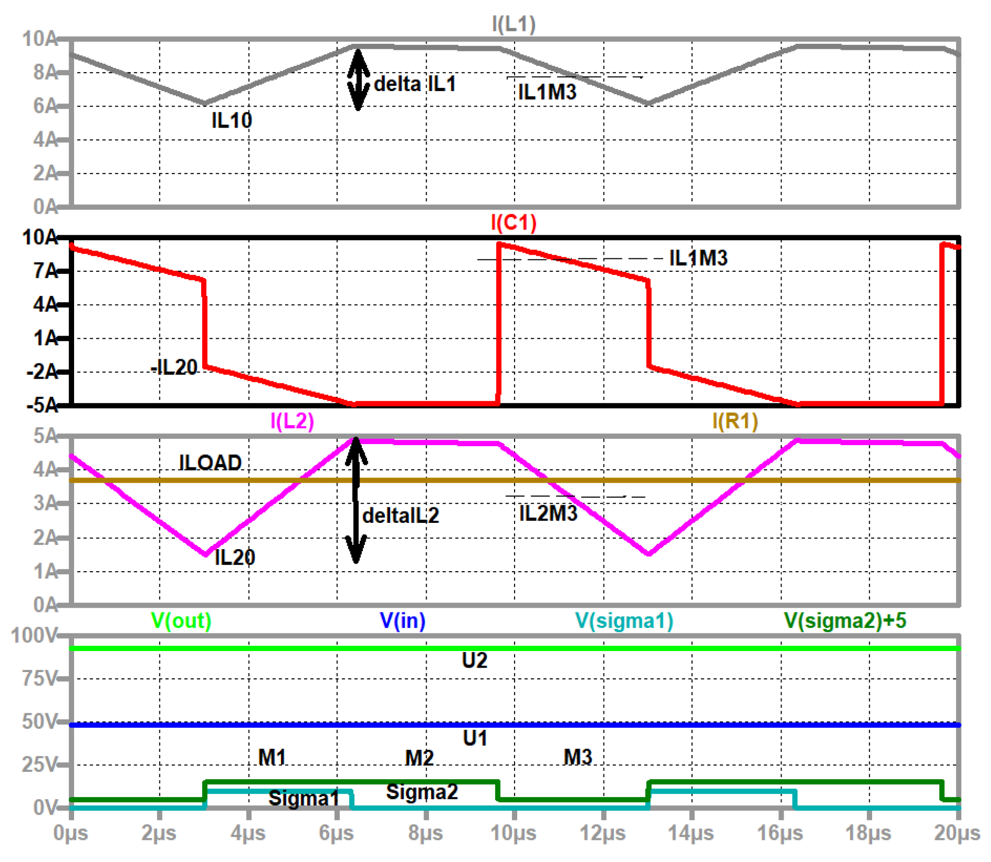
Figure 6.
RLT Buck converter, (a) simulation circuit and (b) up to down: current through the capacitor (violet); current through the coil (red); load current (brown); input voltage (blue); control signal of the second switch (dark green, shifted); output voltage (green); control signal of S1 (turquoise).
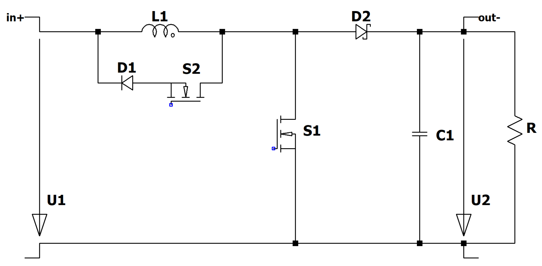
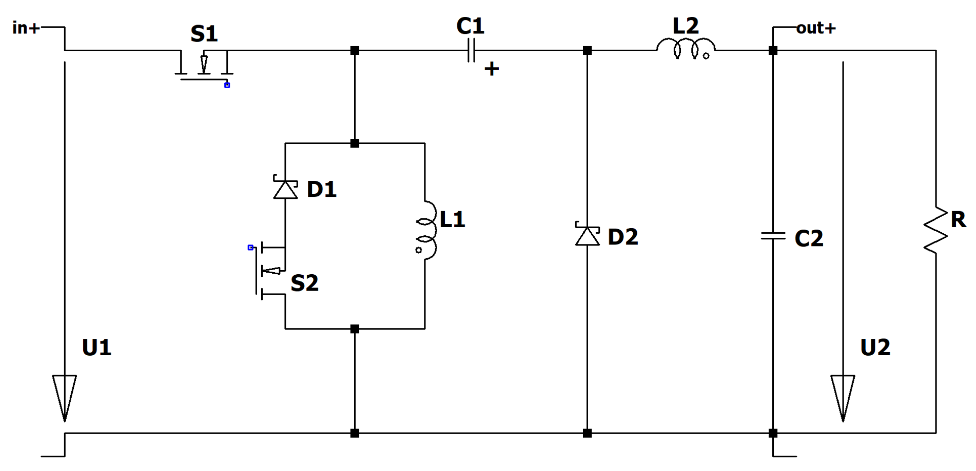
Figure 7.
Circuit diagram of the RLT Buck–Boost converter.
Figure 7.
Circuit diagram of the RLT Buck–Boost converter.
Figure 8.
Voltage transformation ratio of the RLT Buck–Boost: duty cycle of switch S2 is kept constant, duty cycle of switch S1 is used as variable.
Figure 8.
Voltage transformation ratio of the RLT Buck–Boost: duty cycle of switch S2 is kept constant, duty cycle of switch S1 is used as variable.
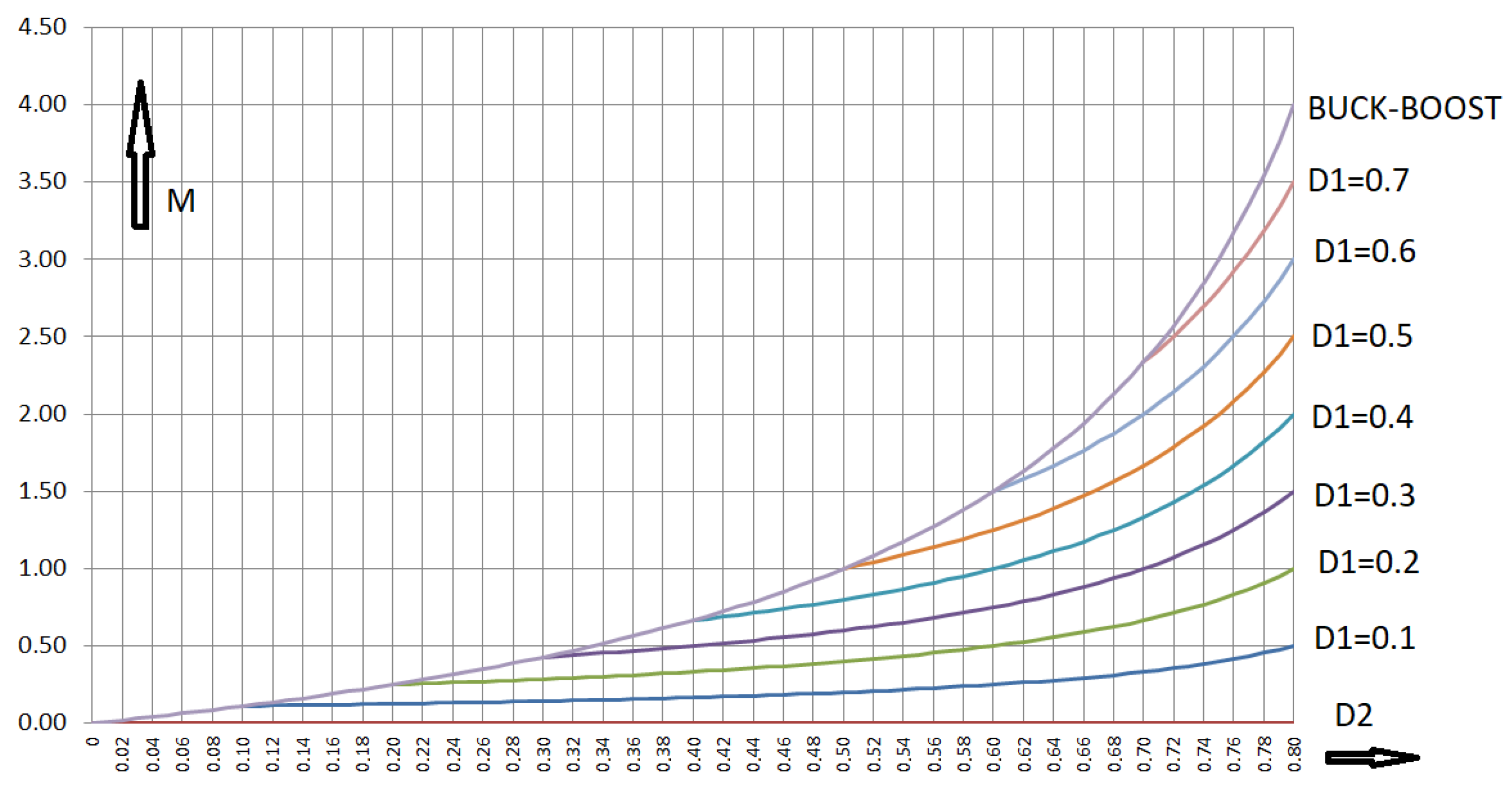
Figure 9.
Voltage transformation ratio of the RLT Buck–Boost: duty cycle of switch S1 is kept constant, duty cycle of switch S2 is used as variable.
Figure 9.
Voltage transformation ratio of the RLT Buck–Boost: duty cycle of switch S1 is kept constant, duty cycle of switch S2 is used as variable.
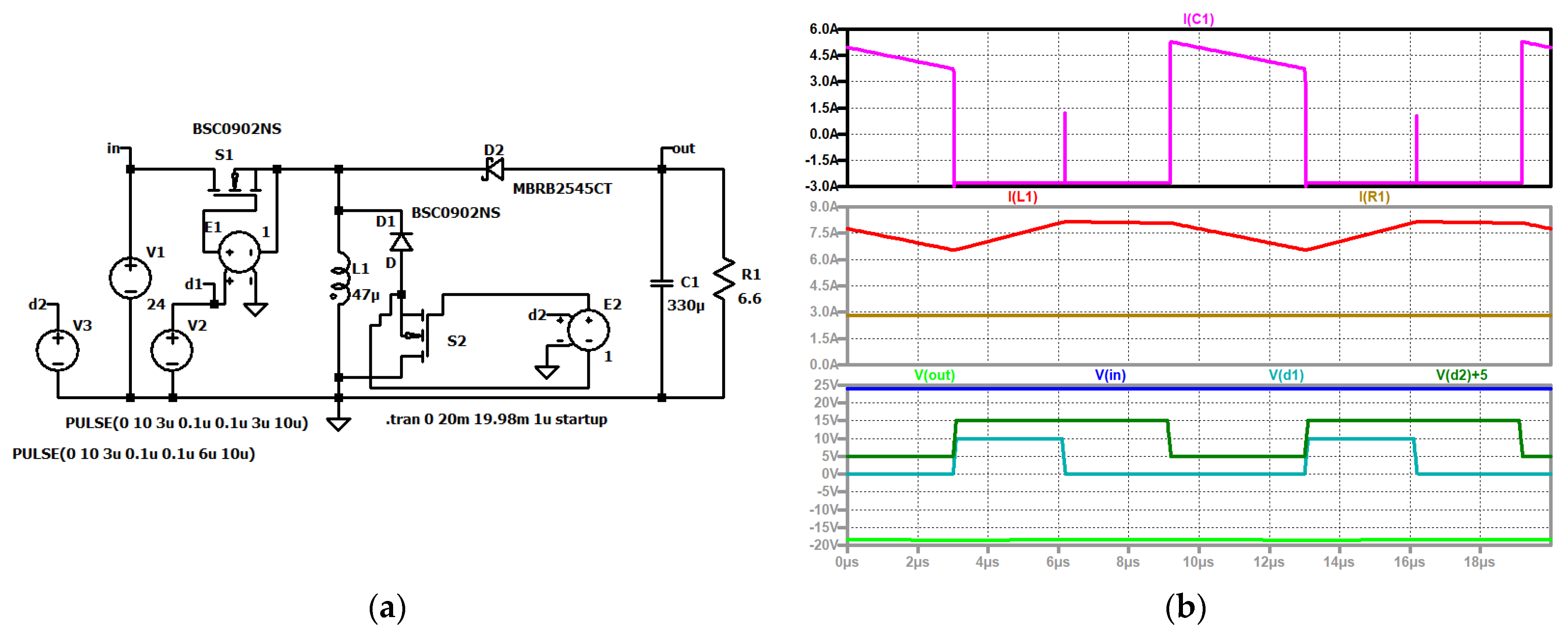
Figure 10.
RLT Buck–Boost converter, (a) simulation circuit, and (b) up to down: current through the output capacitor (violet); current through the coil (red), load current through the load (brown); input voltage (blue), control signal of the second switch (dark green), control signal of the first switch S1 (turquoise), output voltage (green).
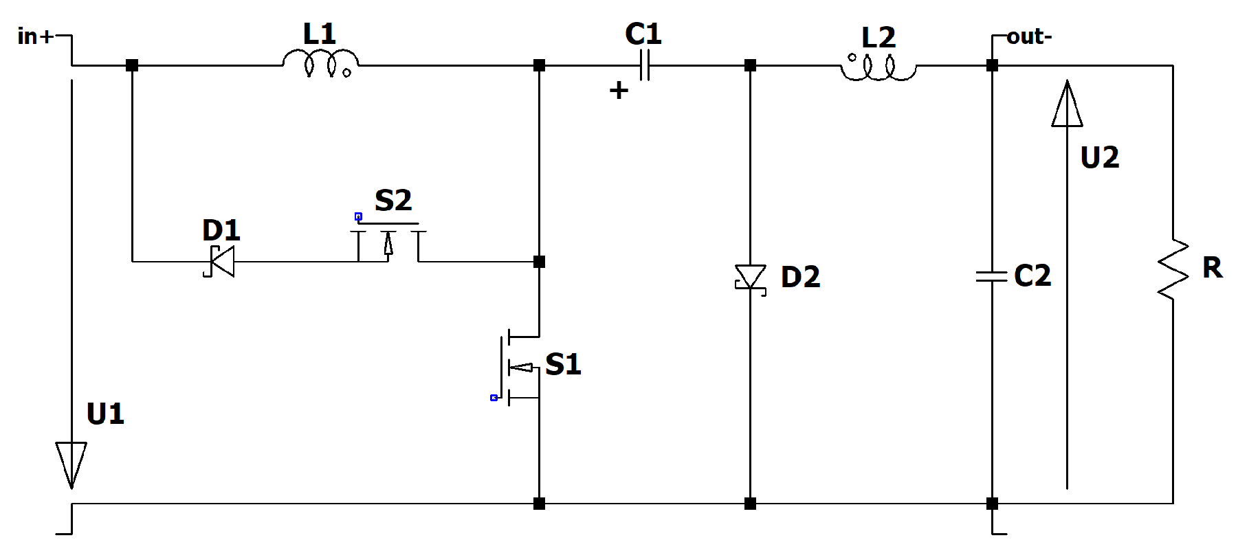
Figure 11.
Circuit diagram of the RLT Boost Converter.
Figure 11.
Circuit diagram of the RLT Boost Converter.
Figure 12.
Voltage transformation ratio of the RLT Boost converter with fixed duty cycle d2 and the duty cycle d1 as variable.
Figure 12.
Voltage transformation ratio of the RLT Boost converter with fixed duty cycle d2 and the duty cycle d1 as variable.
Figure 13.
Voltage transformation ratio of the RLT Boost converter with fixed duty cycle d1 and the duty cycle d2 as variable.
Figure 13.
Voltage transformation ratio of the RLT Boost converter with fixed duty cycle d1 and the duty cycle d2 as variable.
Figure 14.
RLT Boost converter, (a) simulation circuit, and (b) up to down: current through the capacitor (violet); current through the coil (red), load current (brown); output voltage (green), input voltage (blue), control signal of the second switch (dark green), control signal of S1 (turquoise).
Figure 14.
RLT Boost converter, (a) simulation circuit, and (b) up to down: current through the capacitor (violet); current through the coil (red), load current (brown); output voltage (green), input voltage (blue), control signal of the second switch (dark green), control signal of S1 (turquoise).
Figure 15.
Circuit diagram of the RLT-Zeta converter.
Figure 15.
Circuit diagram of the RLT-Zeta converter.
Figure 16.
RLT ZETA converter, (a) simulation circuit, and (b) up to down: current through the intermediate capacitor C1 (grey); current through the second coil L2 (violet), load current (brown); current through the first coil L1 (red); input voltage (blue), output voltage (green), control signal of the second switch (dark green), control signal of first switch (turquoise).
Figure 17.
Circuit diagram of the RLT Cuk converter.
Figure 17.
Circuit diagram of the RLT Cuk converter.
Figure 18.
RLT CUK converter, (a) simulation circuit, and (b) up to down: current through the intermediate capacitor C1 (grey); current through the second coil L2 (violet), load current (brown); current through the first coil L1 (red); input voltage (blue), control signal of the second switch (dark green), control signal of the first switch (turquoise), output voltage (green).
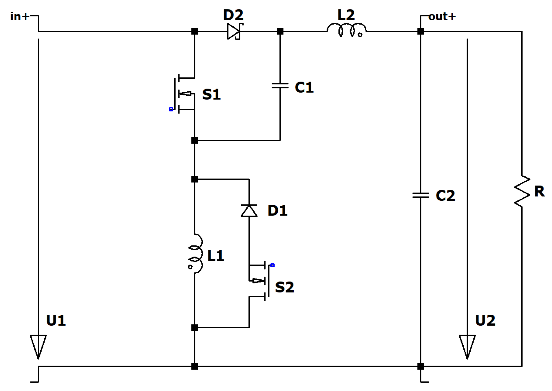
Figure 19.
Circuit diagram of the RLT Cuk converter variant II.
Figure 19.
Circuit diagram of the RLT Cuk converter variant II.
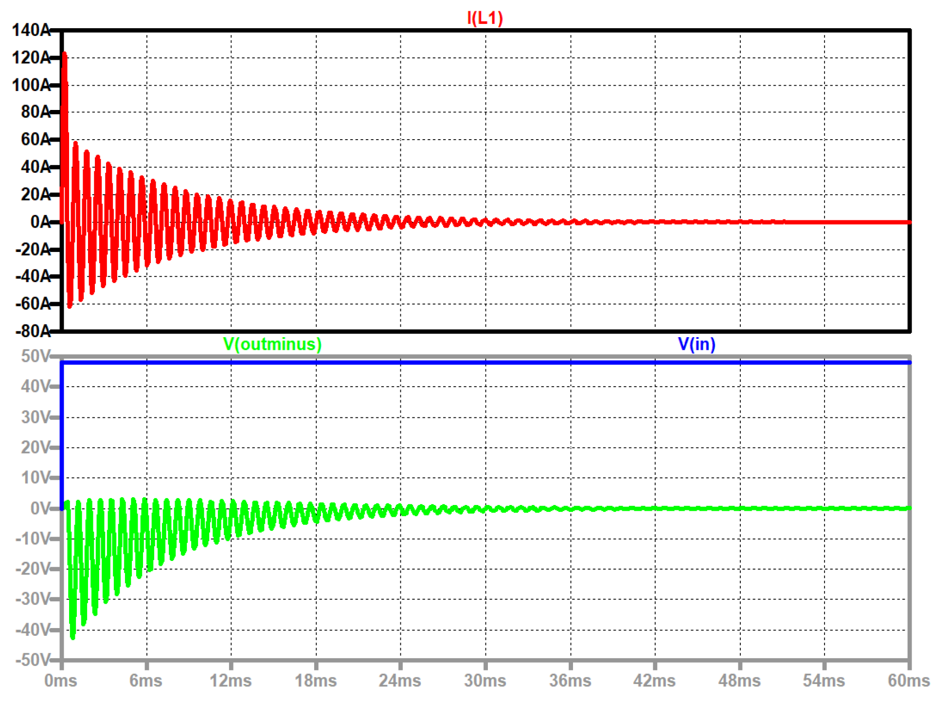
Figure 20.
Inrush of a Cuk converter, up to down: current through inductor L1 (red); input voltage (blue); output voltage (green).
Figure 20.
Inrush of a Cuk converter, up to down: current through inductor L1 (red); input voltage (blue); output voltage (green).
Figure 21.
Circuit diagram of the Super Boost converter.
Figure 21.
Circuit diagram of the Super Boost converter.
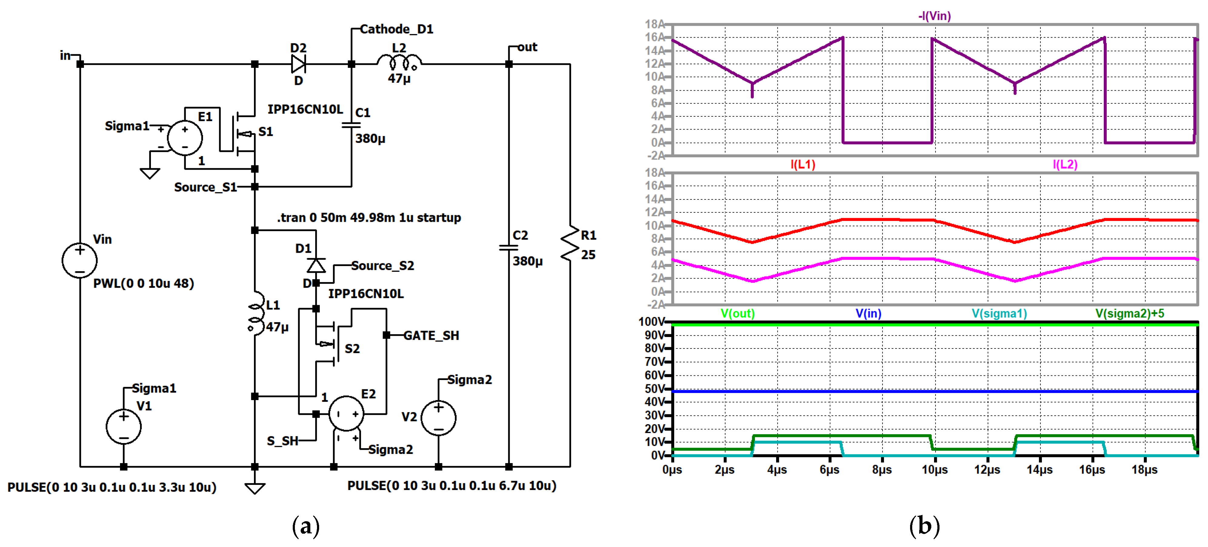
Figure 22.
RLT Super Boost converter, (a) simulation circuit, and (b) up to down: input current (dark violet); current through the first coil L1 (red), current through the second coil L2 (violet); output voltage (green), input voltage (blue), control signal of the second switch (dark green), control signal of the first switch (turquoise).
Figure 23.
RLT Super Boost converter, (a) simulation circuit, and (b) up to down: voltage across D1 (violet); voltage across D2 (red); voltage across S2 (dark blue); voltage across S1 (black); output voltage (green), input voltage (blue), control signal of the second switch (dark green), control signal of S1 (turquoise).
Figure 24.
Circuit diagram of RLT d-square converter.
Figure 24.
Circuit diagram of RLT d-square converter.
Figure 25.
Voltage transformation ratio of the RLT d-square converter, duty cycle of switch S2 as parameter, and duty cycle of switch S1 as variable.
Figure 25.
Voltage transformation ratio of the RLT d-square converter, duty cycle of switch S2 as parameter, and duty cycle of switch S1 as variable.
Figure 26.
Voltage transformation ratio of the RLT d-square converter, duty cycle of switch S1 as parameter, and duty cycle of switch S2 as variable.
Figure 26.
Voltage transformation ratio of the RLT d-square converter, duty cycle of switch S1 as parameter, and duty cycle of switch S2 as variable.
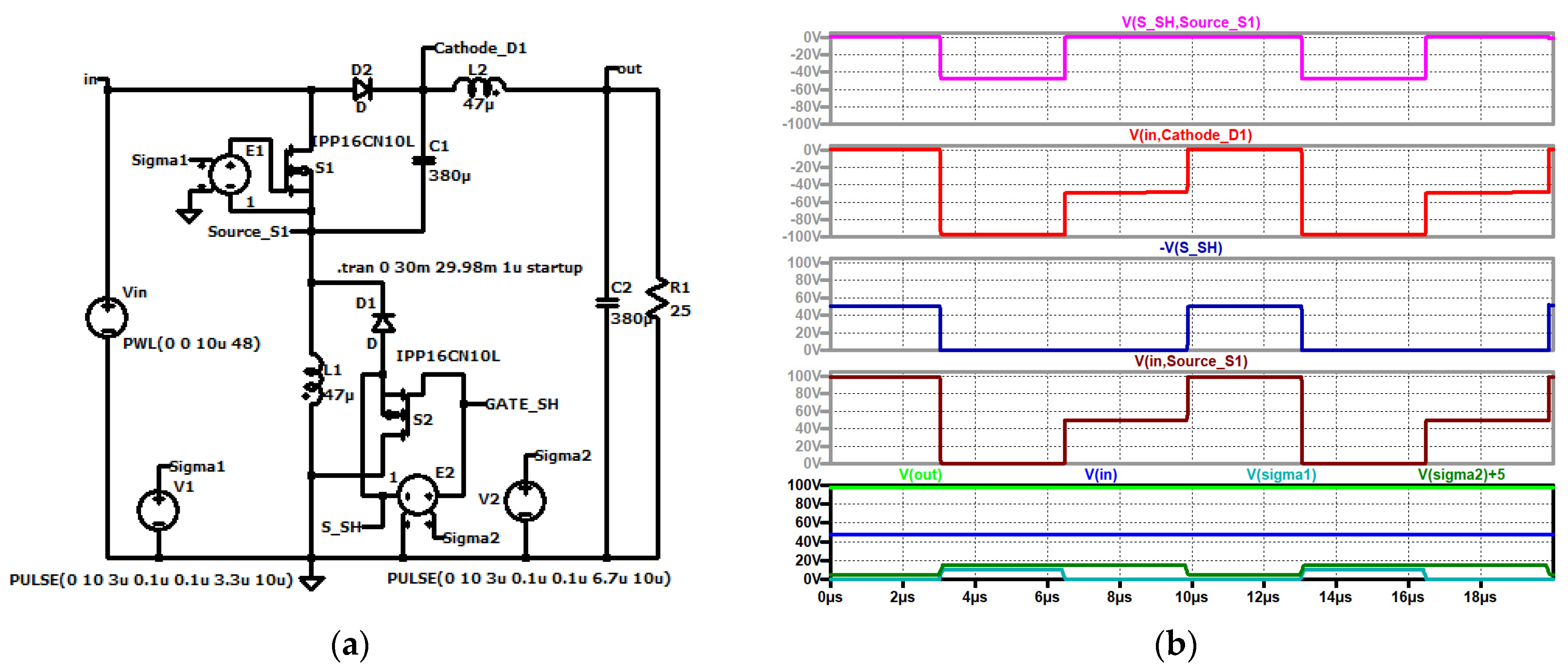
Figure 27.
RLT d-square Buck converter, (a) simulation circuit, and (b) up to down: current through the intermediate capacitor C1 (grey); current through the second coil L2 (violet), load current (brown); current through the first coil L1 (red); input voltage (blue), control signal of the second switch (dark green), output voltage (green), control signal of S1 (turquoise).
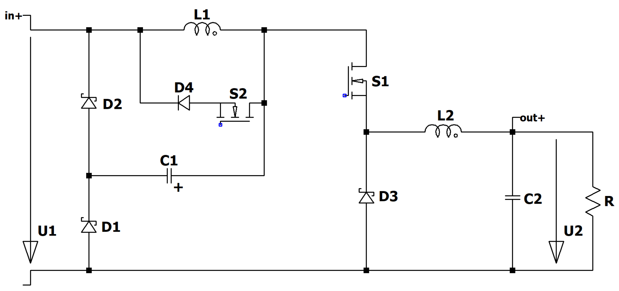
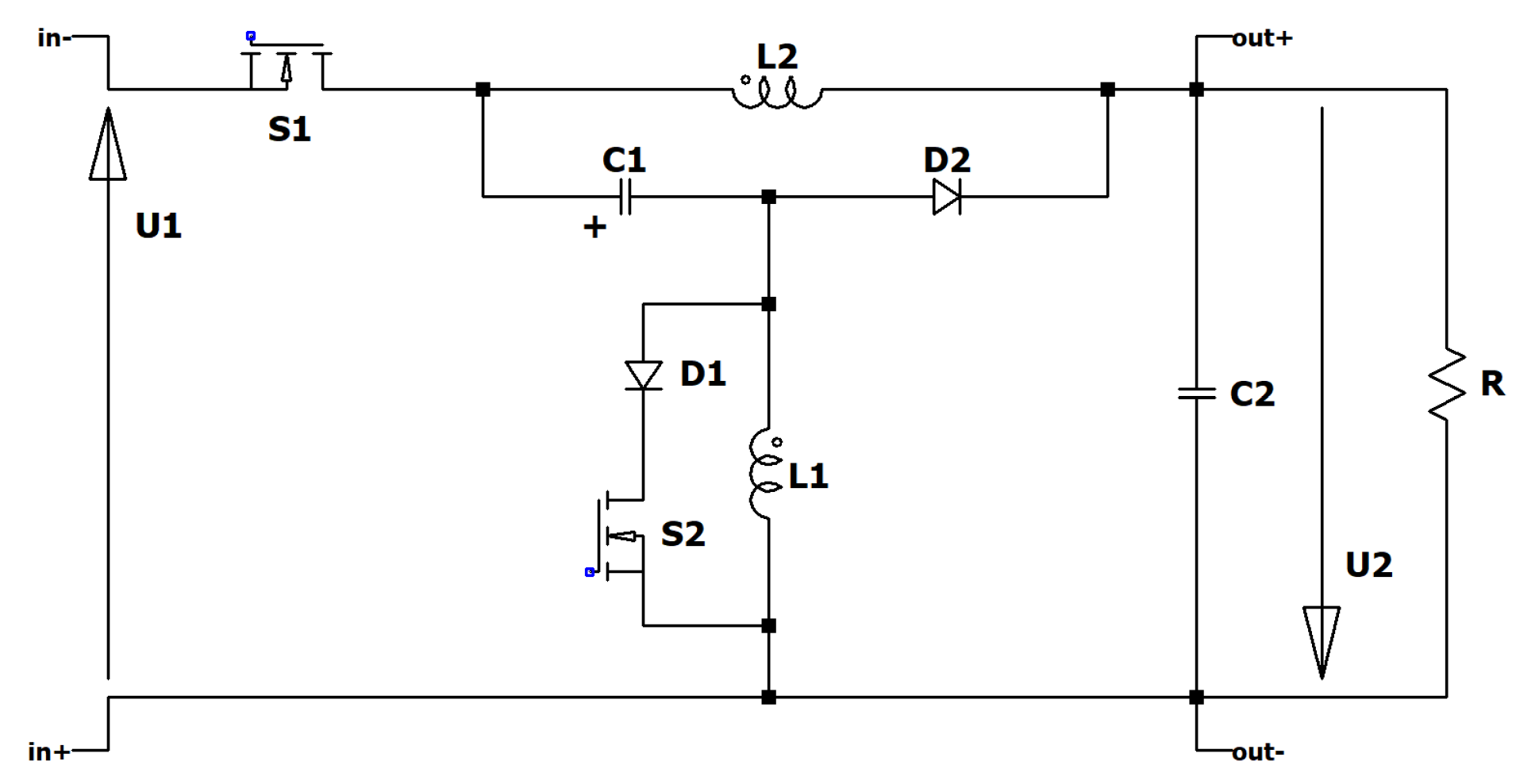
Figure 28.
RLT D1/(1 − D1 − D2) converter.
Figure 28.
RLT D1/(1 − D1 − D2) converter.
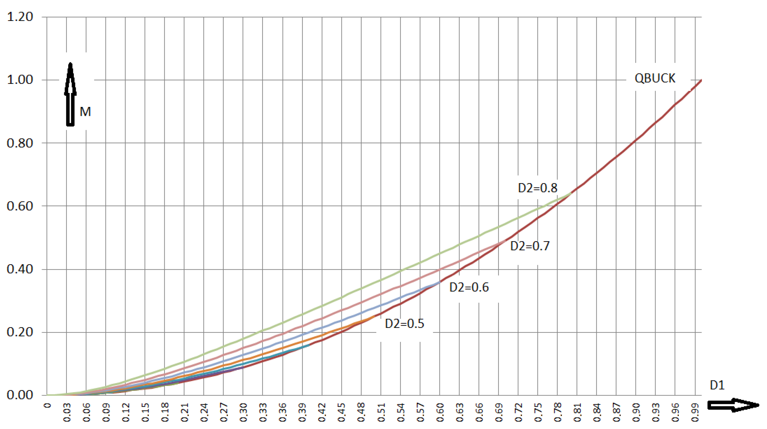
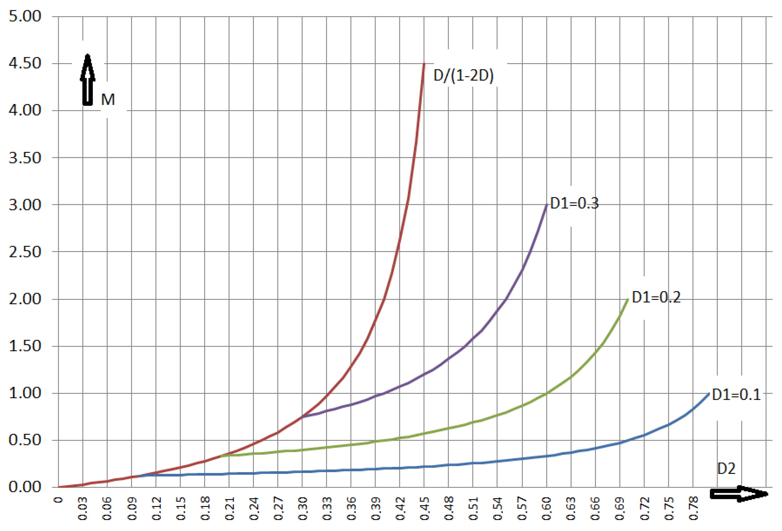
Figure 29.
Voltage transformation ratio of the RLT D1/(1 − D1 − D2) converter, duty cycle of switch S2 as parameter, and duty cycle of switch S1 as variable.
Figure 29.
Voltage transformation ratio of the RLT D1/(1 − D1 − D2) converter, duty cycle of switch S2 as parameter, and duty cycle of switch S1 as variable.
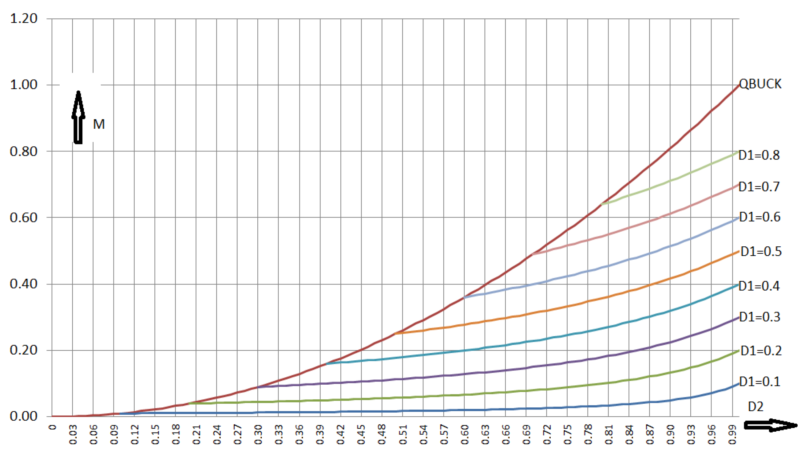
Figure 30.
Voltage transformation ratio of the RLT D1/(1 − D1 − D2) converter, duty cycle of switch S1 as parameter, and duty cycle of switch S2 as variable.
Figure 30.
Voltage transformation ratio of the RLT D1/(1 − D1 − D2) converter, duty cycle of switch S1 as parameter, and duty cycle of switch S2 as variable.
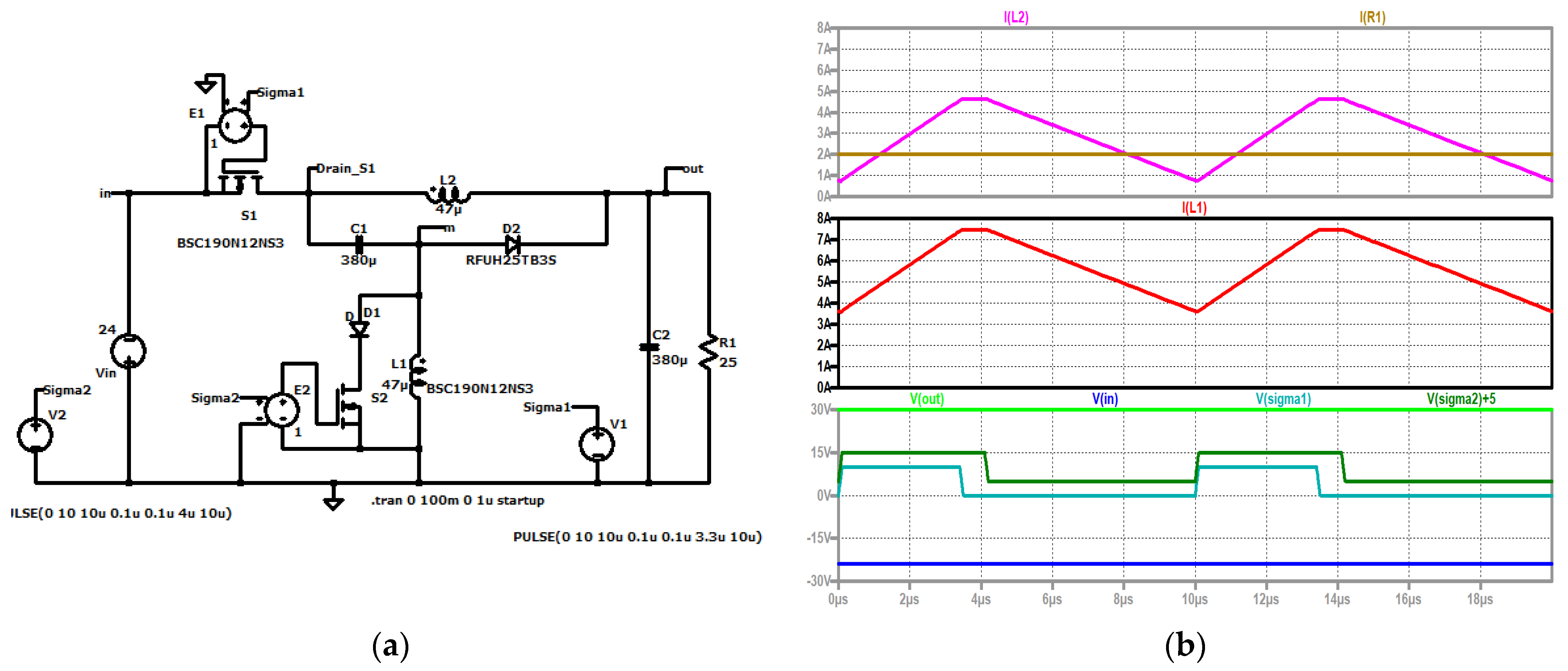
Figure 31.
RLT D1/(1 − D1 − D2) converter, (a) simulation circuit, and (b) up to down: current through the second coil L2 (violet), load current (brown); current through the first coil L1 (red); output voltage (green), control signal of the second switch (dark green), control signal of S1 (turquoise), input voltage (blue).
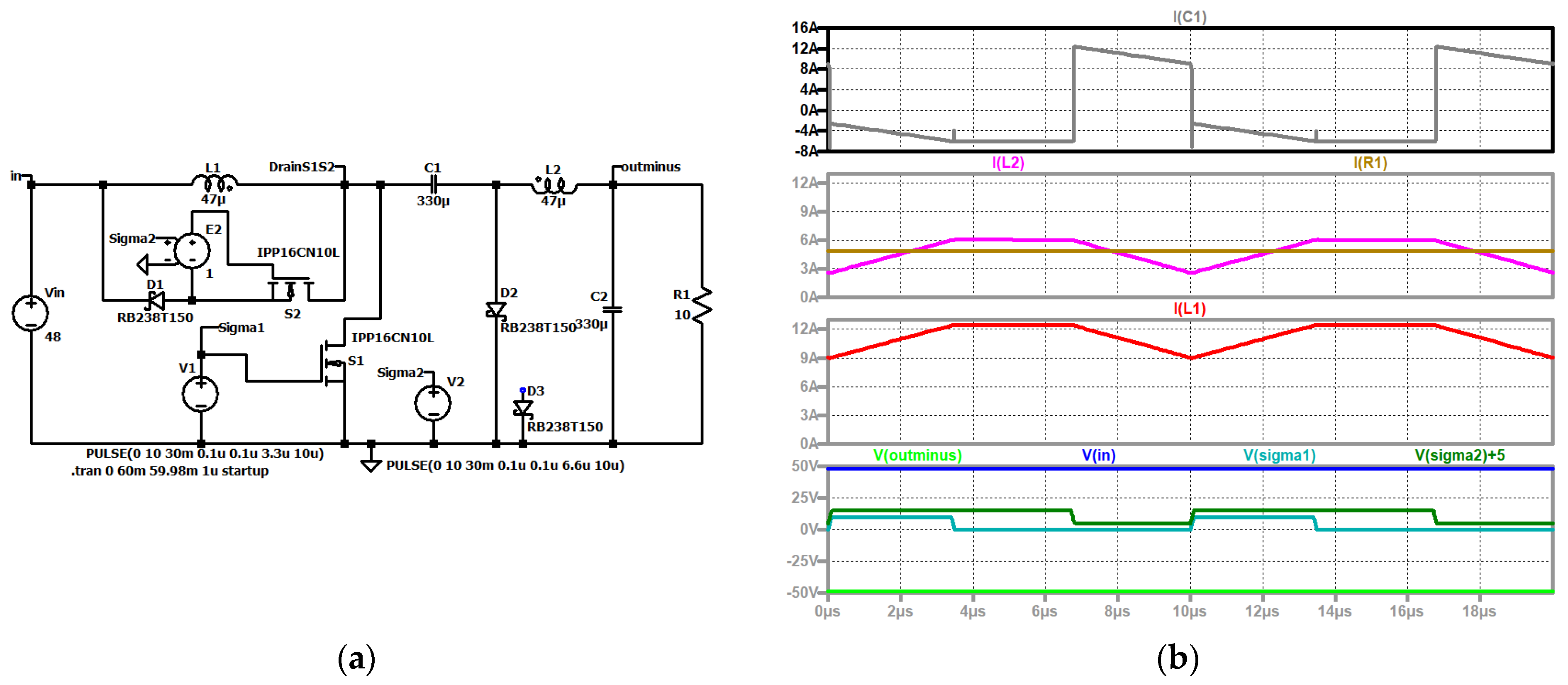
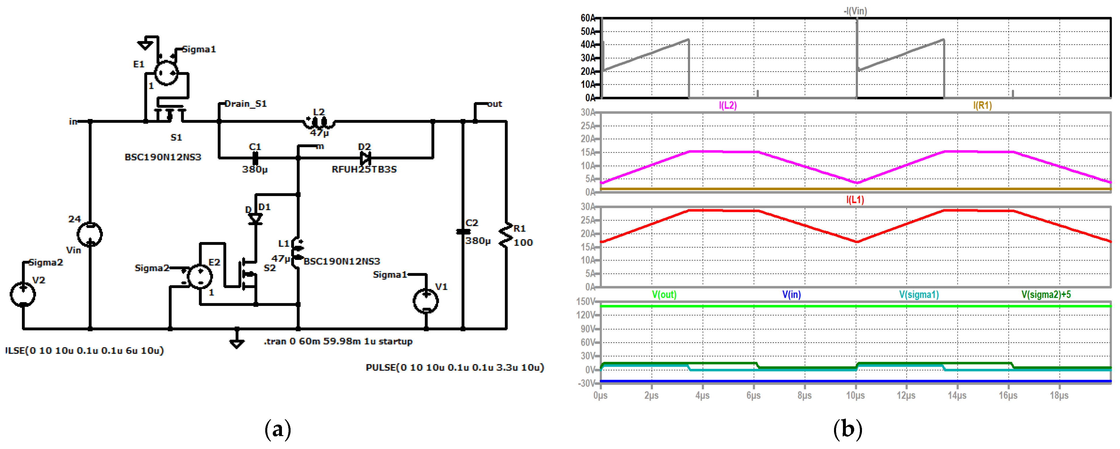
Figure 32.
RLT D1/(1 − D1 − D2) converter, (a) simulation circuit, (b) and up to down: input current (grey); current through the second coil L2 (violet), load current (brown); current through the first coil L1 (red); output voltage (green), control signal of the second switch (dark green), control signal of S1 (turquoise), input voltage (blue).
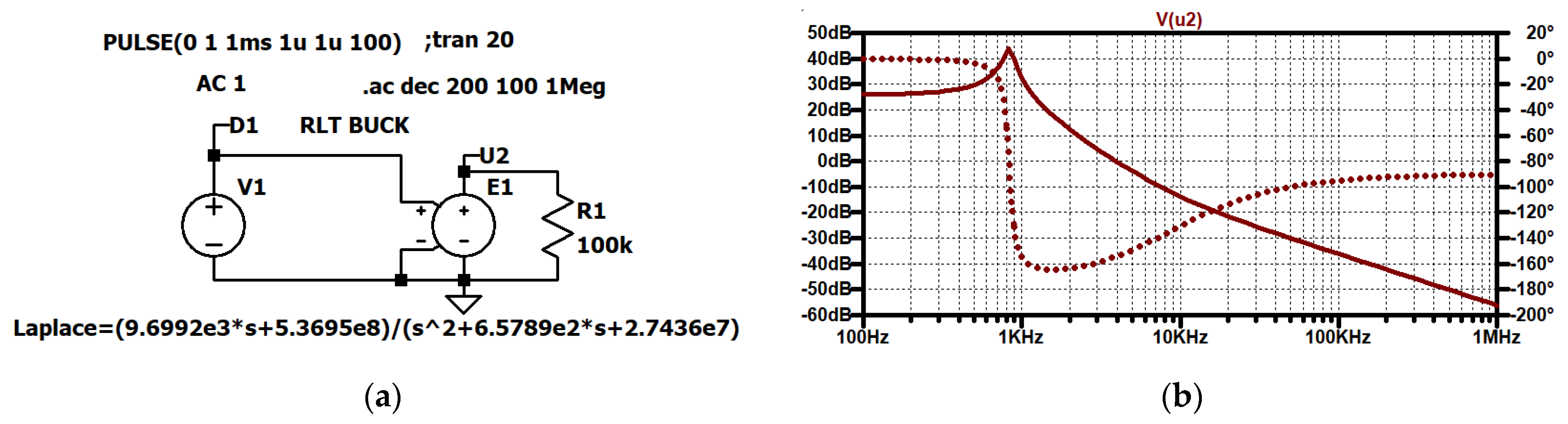
Figure 33.
RLT Buck converter, output voltage U2 referred to the duty cycle D1, transfer function: (a) simulation circuit, (b) Bode plot (solid line: gain response, dotted line: phase response).
Figure 33.
RLT Buck converter, output voltage U2 referred to the duty cycle D1, transfer function: (a) simulation circuit, (b) Bode plot (solid line: gain response, dotted line: phase response).
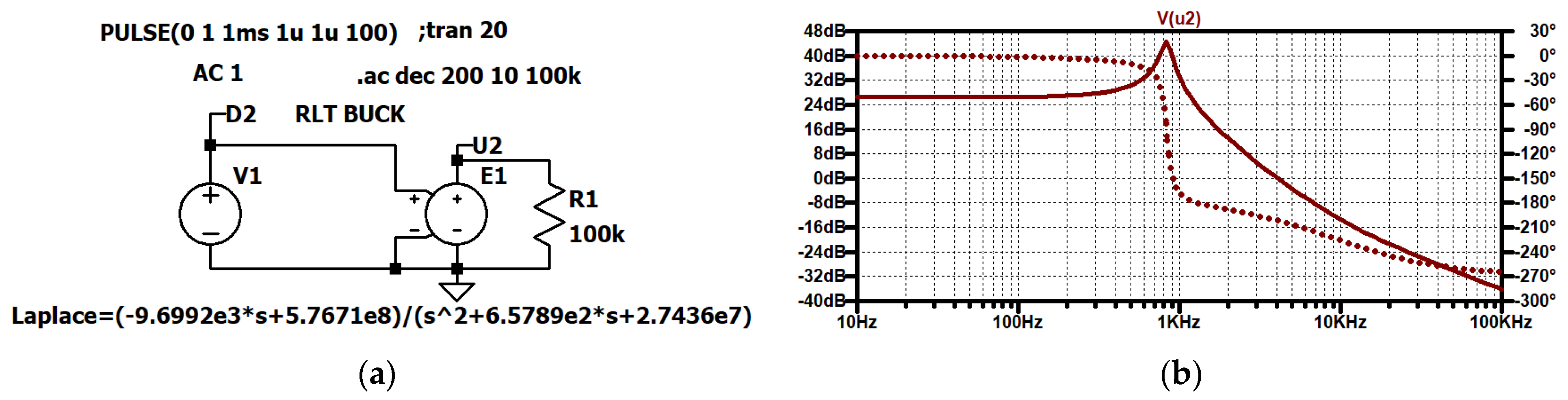
Figure 34.
RLT Buck converter, output voltage U2 referred to the duty cycle D2, transfer function: (a) simulation circuit, (b) Bode plot (solid line: gain response, dotted line: phase response).
Figure 34.
RLT Buck converter, output voltage U2 referred to the duty cycle D2, transfer function: (a) simulation circuit, (b) Bode plot (solid line: gain response, dotted line: phase response).
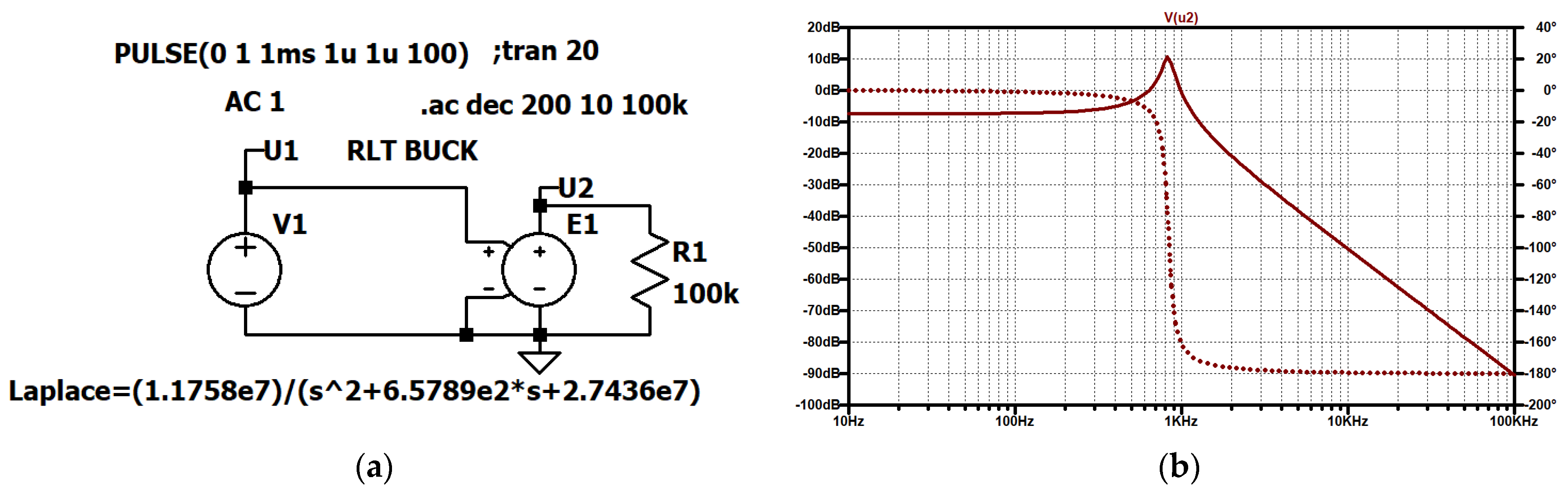
Figure 35.
RLT Buck converter, output voltage U2 referred to the input voltage U1 transfer function: (a) simulation circuit, (b) Bode plot (solid line: gain response, dotted line: phase response).
Figure 35.
RLT Buck converter, output voltage U2 referred to the input voltage U1 transfer function: (a) simulation circuit, (b) Bode plot (solid line: gain response, dotted line: phase response).
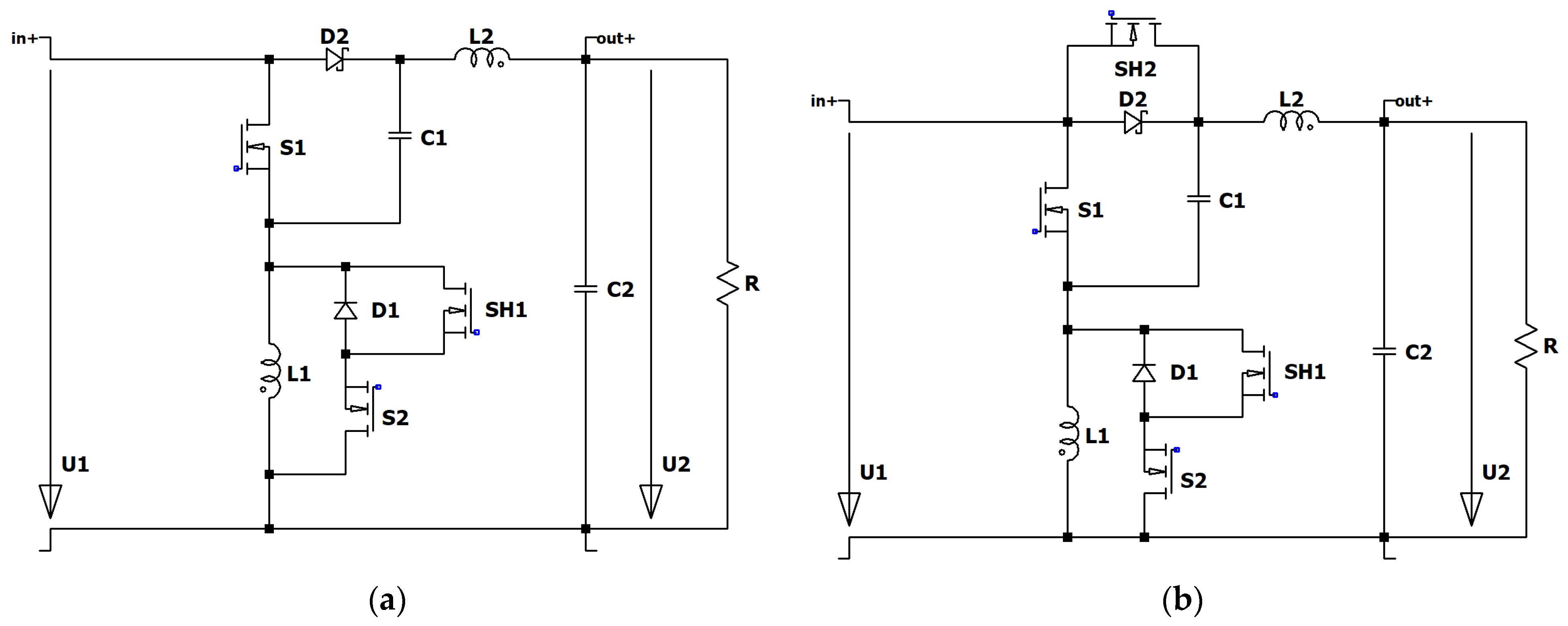
Figure 36.
RLT Super Boost with efficiency improvement, (a) with improved bypass, and (b) with two auxiliary switches.
Figure 36.
RLT Super Boost with efficiency improvement, (a) with improved bypass, and (b) with two auxiliary switches.
Figure 37.
Super Boost converter, up to down: current through L1 (grey); current through the capacitor C1 (red); current through L2 (violet), load current (brown); output voltage (green), input voltage (blue), control signal of S2 (dark green), control signal of S1 (turquoise).
Figure 37.
Super Boost converter, up to down: current through L1 (grey); current through the capacitor C1 (red); current through L2 (violet), load current (brown); output voltage (green), input voltage (blue), control signal of S2 (dark green), control signal of S1 (turquoise).
Table 1.
Voltage stress across the semiconductors of the second-order converters.
Table 1.
Voltage stress across the semiconductors of the second-order converters.
| | S1 | S2 | D1 | D2 |
|---|
| Buck | U1 | U2 | U1 | U1 |
| Boost | U2 | U2 − U1 | U1 | U2 |
| Buck–Boost | U1 + U2 | U2 | U1 | U1 + U2 |
Table 2.
Voltage stress across the semiconductors of the fourth-order converters.
Table 2.
Voltage stress across the semiconductors of the fourth-order converters.
| | S1 | S2 | D1 | D2 |
|---|
| RLT Zeta | U1 + U2 | U2 | U1 | U2 |
| RLT Cuk | U1 + U2 | U1 | U1 | U1 + U2 |
| RLT Super Boost | U2 | U2 − U1 | U1 | U2 |
| RLT D1/(1 − D1 − D2) | 2U2 + U1 | U2 | U1 + U2 | 2U2 + U1 |
Table 3.
Voltage stress across the semiconductors of the d-square Buck converter.
Table 3.
Voltage stress across the semiconductors of the d-square Buck converter.
| | S1 | S2 | D1 | D2 | D3 | D4 |
|---|
| D-SquareBuck | U1·(1 + D1) | U1·D1 | U1 | U1 | D1·U1 | U1·(1 − D1) |
Table 4.
Currents through the components of the second-order converters.
Table 4.
Currents through the components of the second-order converters.
| | | | | | |
|---|
| Buck | | | | | |
| Buck–Boost | | | | | |
| Boost | | | | | |
Table 5.
Currents through the components of the fourth-order converters.
Table 5.
Currents through the components of the fourth-order converters.
| | | | | | | |
|---|
Zeta,
Cuk,
Super Boost | | 1 | | | | |
Table 6.
Currents through the components of the d-square Buck converter.
Table 6.
Currents through the components of the d-square Buck converter.
| | | | | | | | |
|---|
| D-Square Buck | | 1 | | | | | |
Table 7.
Currents through the components of the D1/(1-D1+D2) converter.
Table 7.
Currents through the components of the D1/(1-D1+D2) converter.
| | | | | | | |
|---|
| D1/(1 − D1 + D2) | | | | | | |
Table 8.
Continuous or discontinuous input and output currents.
Table 8.
Continuous or discontinuous input and output currents.
| | Buck | Buck–Boost | Boost | Zeta | Cuk I | Cuk II | Super Boost | Quadratic Buck | D1/(1 − D1 − D2) |
|---|
| IN | D | D | D | D | D | C | D | D | D |
| OUT | D | D | D | C | C | D | C | C | D |
Table 9.
Inrush? YES (Y) or NO (N).
Table 9.
Inrush? YES (Y) or NO (N).
| | Buck | Buck–Boost | Boost | Zeta | Cuk I | Cuk II | Super Boost | Quadratic Buck | D1/(1 − D1 − D2) |
|---|
| INRUSH | N | N | Y | N | Y | Y | Y | N | N |


