Article

High-Precision Low-Power Interface Circuit for Two-Dimensional Integrated Magnetic Switches

1
School of Microelectronics, Tianjin University, Tianjin 300072, China
2
Tianjin Key Laboratory of Imaging and Sensing Microelectronics, Tianjin 300072, China
*
Authors to whom correspondence should be addressed.
Electronics 2025, 14(7), 1299; https://doi.org/10.3390/electronics14071299
Submission received: 25 February 2025 / Revised: 19 March 2025 / Accepted: 24 March 2025 / Published: 26 March 2025

Abstract

:
This paper proposes a high-precision low-power interface circuit for two-dimensional (2D) integrated magnetic switches that can detect 2D magnetic fields and output 5 V CMOS digital signals. The interface circuit combines chopper stabilization and output offset storage technology to effectively suppress the offset of the entire signal chain and significantly improve detection accuracy. Additionally, an architecture-level signal processing algorithm is proposed, which not only realizes full polarity detection of the magnetic field at a low cost but also realizes switch detection of multi-dimensional magnetic fields in the interface circuit without additional processing. Furthermore, the circuit provides flexible adjustment of both switch trip thresholds and hysteresis windows through 4-bit off-chip trimming codes, which greatly enhances the universality of the interface circuit. This chip is implemented using 180 nm BCD technology with a chip area of 1.18 mm 2 . The measurement results show that the interface circuit can simultaneously process 2D input signals with a resolution of less than 85 μV. In addition, through a 4-bit trim code, the interface circuit can adjust the switch trip threshold in the range of 0–13.52 mV and the hysteresis interval in the range of 0–7.32 mV. The average current consumption of the chip is 6.757 μA.

1. Introduction

With the iterative advancement of modern electronic technology, sensing technology has deeply penetrated all areas of human production and life [1]. As a typical representative of non-contact detection technology, magnetic switches enable the precise detection of displacement states, motion trajectories, and mechanical actions through the principle of magnetic field coupling [2], and exhibit excellent anti-mechanical vibration characteristics and high sensitivity.
The magnetic induction switches currently on the market are generally one-dimensional (1D) sensors [3,4], but, due to their lack of sensitivity to the direction of the magnetic field, they face significant limitations in wide-angle magnetic sensing applications. As an important component of the integrated magnetic switch, the interface circuit is the key to achieving high-precision, low-power, and multi-dimensional sensing. Affected by non-ideal factors such as process deviations, temperature drift, and packaging stress, the input offset voltage of CMOS operational amplifiers that have not undergone offset calibration generally reaches the millivolt level [5,6], which will significantly degrade the effective detection accuracy of the magnetic switch for magnetic sensitive devices with low output voltage characteristics such as silicon-based hall elements [7,8]. In terms of energy efficiency optimization, the kiloohm-level internal resistance of magnetic sensitive elements results in milliampere-level static current losses, which significantly contradicts the trend toward miniaturization and low power consumption in modern sensing systems. In addition, as shown in Table 1, due to the different sensitivities of different types of magnetic sensor elements, a set of interface circuits needs to be customized for different types of magnetic sensor elements. This behavior of reinventing the wheel will greatly waste manpower and material resources.
In order to achieve multi-dimensional detection, reference [10] designed a three-dimensional (3D) integrated magnetic switch, but its interface circuit only amplifies and compares the input signals in three dimensions, respectively. The detection results in the three dimensions are independent of each other and require additional digital signal processing. In terms of high-precision detection, reference [11] used chopping technology to suppress the offset of the first stage of the instrumentation amplifier in the interface circuit, but did not process the offset of the entire signal chain of the entire interface circuit, which would result in a relatively large residual offset. In addition, reference [12,13] did not perform any offset suppression on the interface circuit. In terms of versatility, relatively few studies have been published.
The 2D magnetic switches can not only solve the problem of 1D magnetic switches’ sensitivity to magnetic field direction but also significantly reduce costs and power consumption compared with 3D magnetic switches. These advantages make them particularly suitable for position detection requiring wide magnetic field sensing angles, such as industrial liquid level position detection, smart meter anti-magnetic attack detection, etc. This paper studies the dedicated interface circuit of 2D magnetic switches. We combined chopper stabilization and output offset storage technology to effectively suppress the overall circuit offset. Through both the physical circuit and the proposed switch generation algorithm, the 2D omnidirectional and omnipolar switch detection was achieved at low cost without the need for additional digital signal processing. In addition, clock-controlled micro-power technology was used to significantly reduce the chip power consumption without affecting the performance of the 2D magnetic switch signal processing chip. Finally, off-chip trim technology was used to achieve a custom configuration of the switching threshold and hysteresis range, enhancing the versatility of the 2D magnetic switch interface circuit application.
In Section 1, we introduce the research background and significance of 2D integrated magnetic switches and the interface circuit. Section 2 analyzes the basic detection principles of 2D integrated magnetic switches. In Section 3, the design of a high-precision low-power interface circuit for 2D integrated magnetic switches is introduced. In Section 4, the chip measurement results are discussed. Finally, Section 5 provides the conclusion.

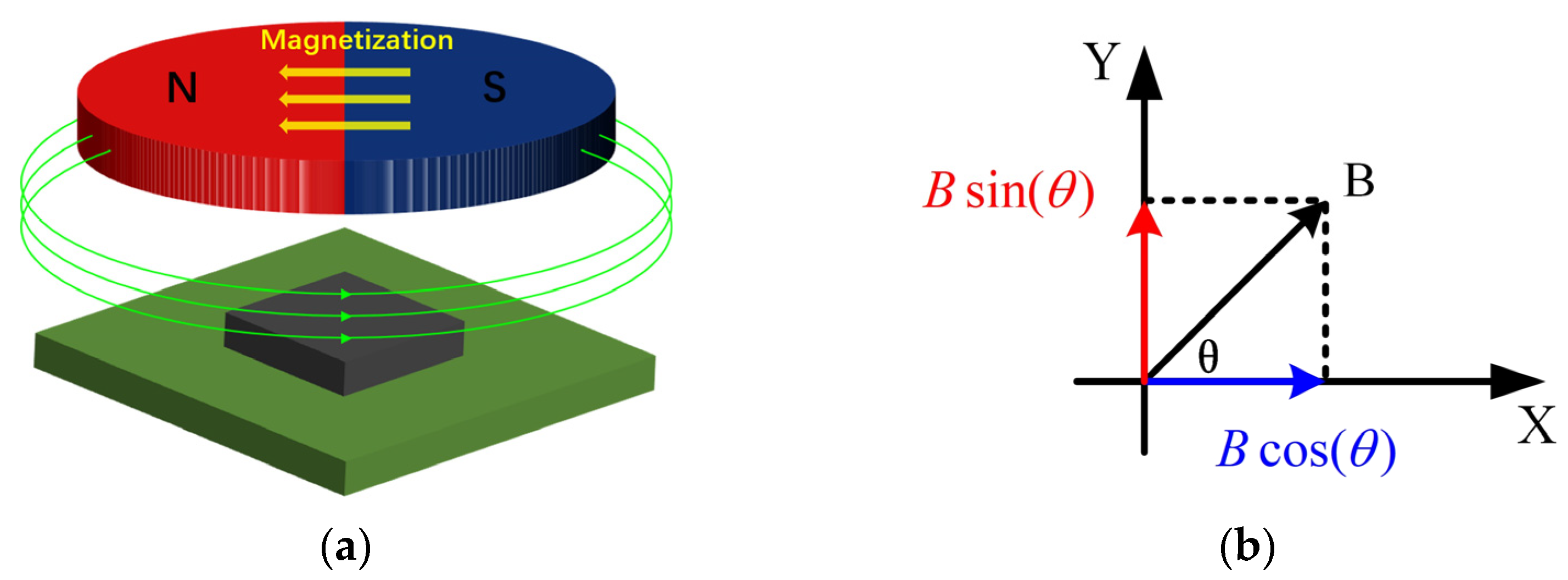
2. Basic Detection Principle of the 2D Integrated Magnetic Switch

In practical applications, the NS pole plane of the magnet is parallel to the chip plane, as shown in Figure 1a, so that the magnetic flux lines emitted by the magnet are parallel to the chip surface. By decomposing the magnetic induction intensity in the chip plane into vertical and horizontal components, two mutually perpendicular magnetic induction vectors are obtained, as shown in Figure 1b.
Two mutually perpendicular magnetic induction intensity vectors are detected by two 1D magnetic sensing elements, such as magnetoresistive bridge, Hall element, etc., to convert the magnetic signals into electrical signals. Subsequently, the electrical signals from these two elements are processed by the 2D integrated magnetic switch interface circuit to determine whether a switch action should be triggered.
In this design, when the absolute value of the differential output voltage from either of the two 1D magnetic sensing elements exceeds the predefined threshold, the interface circuit triggers the switch action, thereby enabling a 2D magnetic field threshold judgment. The threshold window is illustrated in Figure 2, where V B is the voltage corresponding to the total magnetic induction intensity in the plane where the chip is located, V X is the voltage in the X direction, V Y is the voltage in the Y direction, V o p is the operating point voltage, and V r p is the release point voltage. Based on the 360° switch threshold achieved by the interface circuit in this paper, when combined with magnetic sensing elements, it can achieve linear position switch measurement.

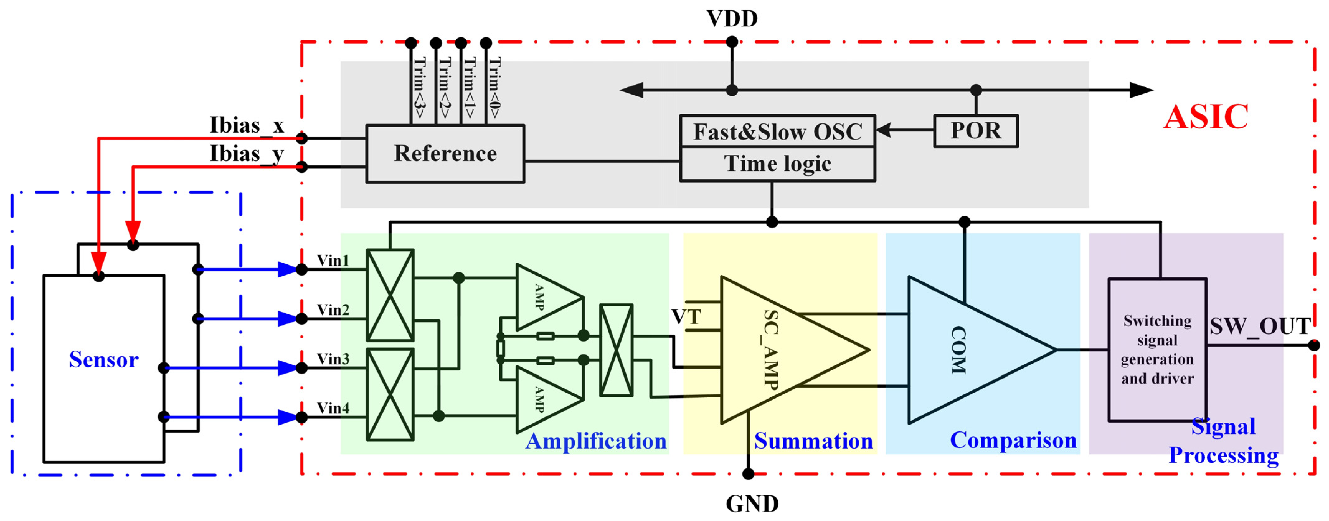
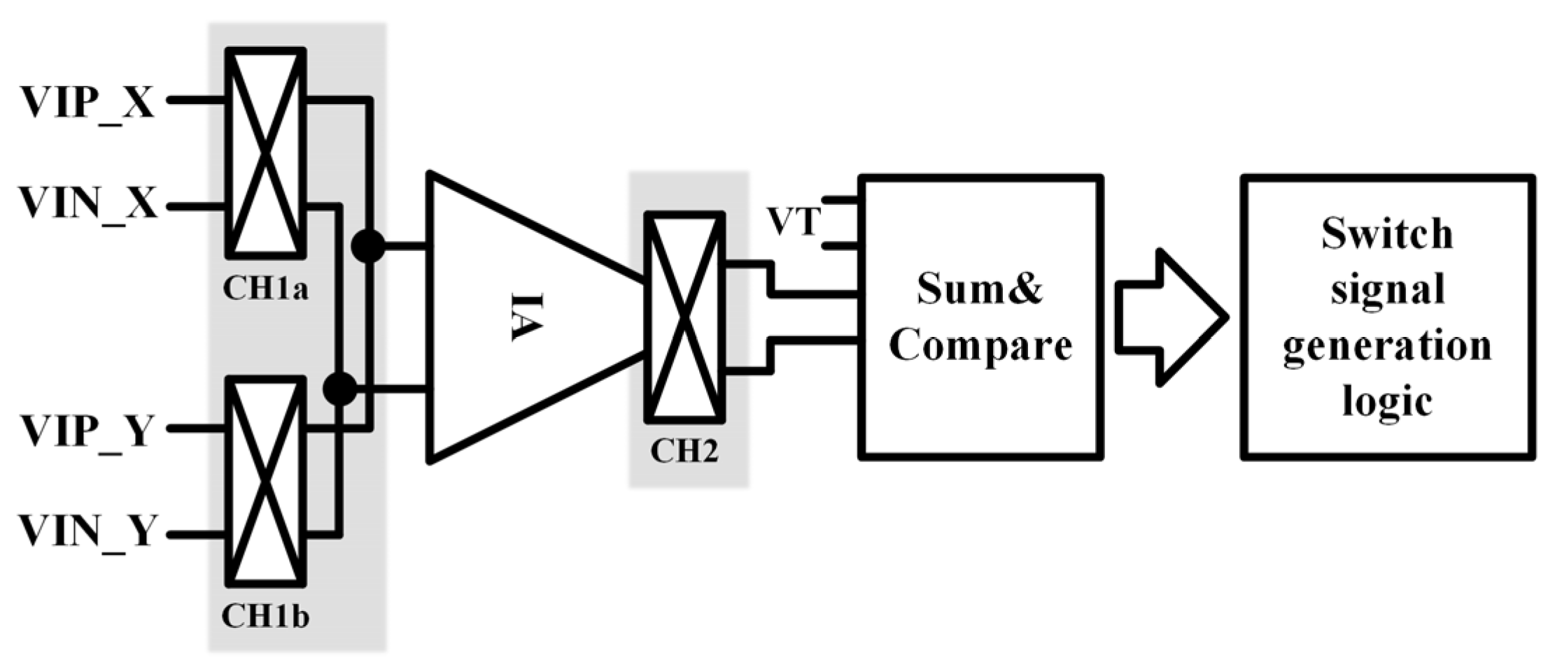
3. Interface Circuit Architecture and Principle

Figure 3 illustrates the block diagram of the 2D integrated magnetic switch interface circuit architecture, comprising the amplification module, summation module, comparison module, switching signal generation and driving module, and auxiliary module. The 2D magnetic field information is detected by orthogonal 1D magnetic sensing elements aligned along the X and Y axes, which convert the magnetic signals into electrical signals. Subsequently, the electrical signals undergo amplification, sampling, summation, and comparison, followed by algorithmic processing to ultimately generate and output a 5 V CMOS digital switch signal.

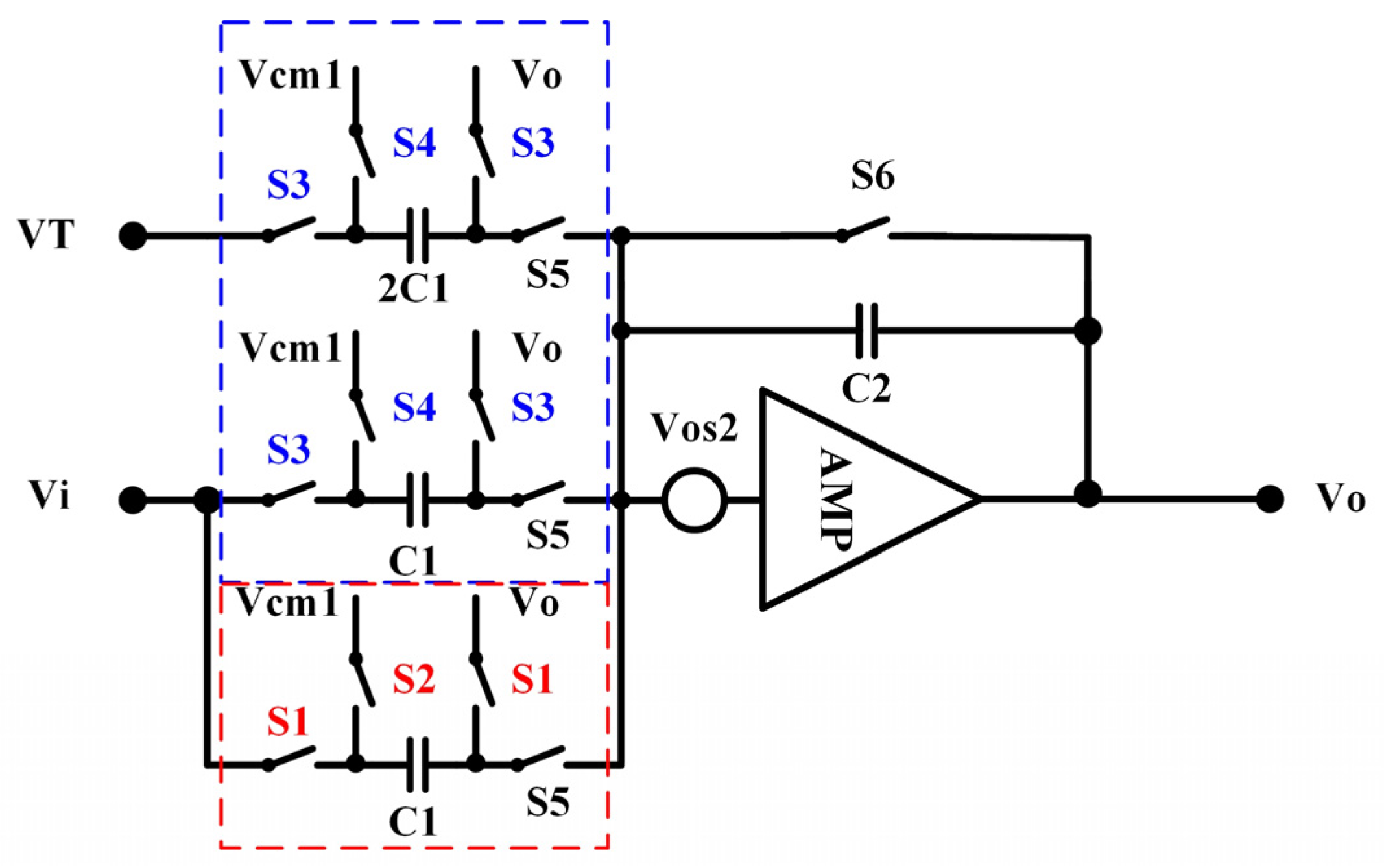
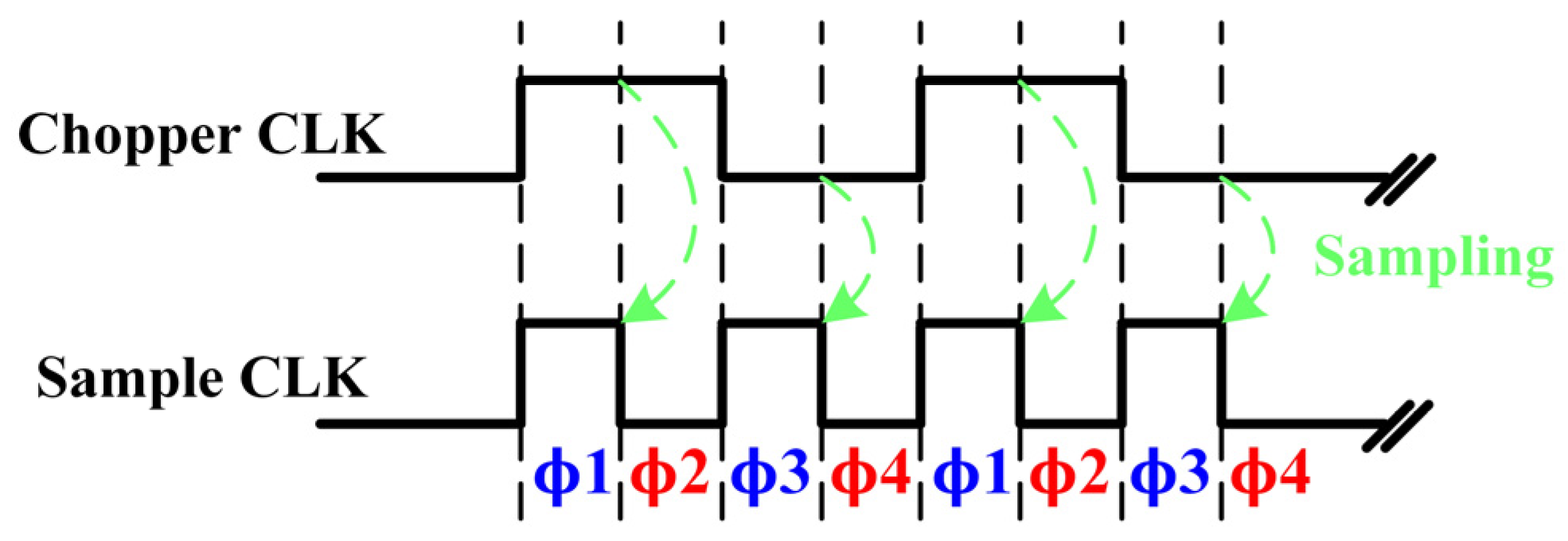
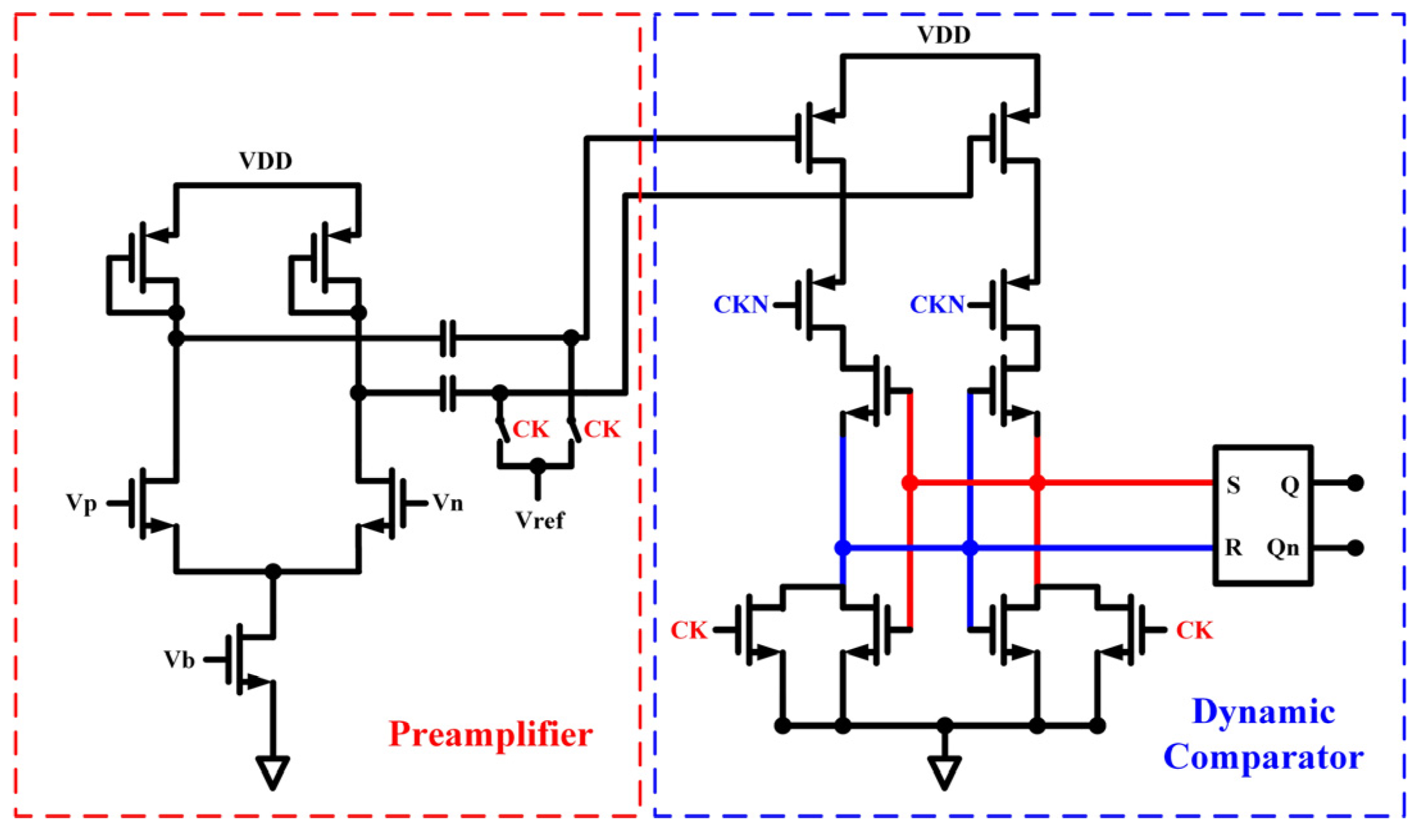
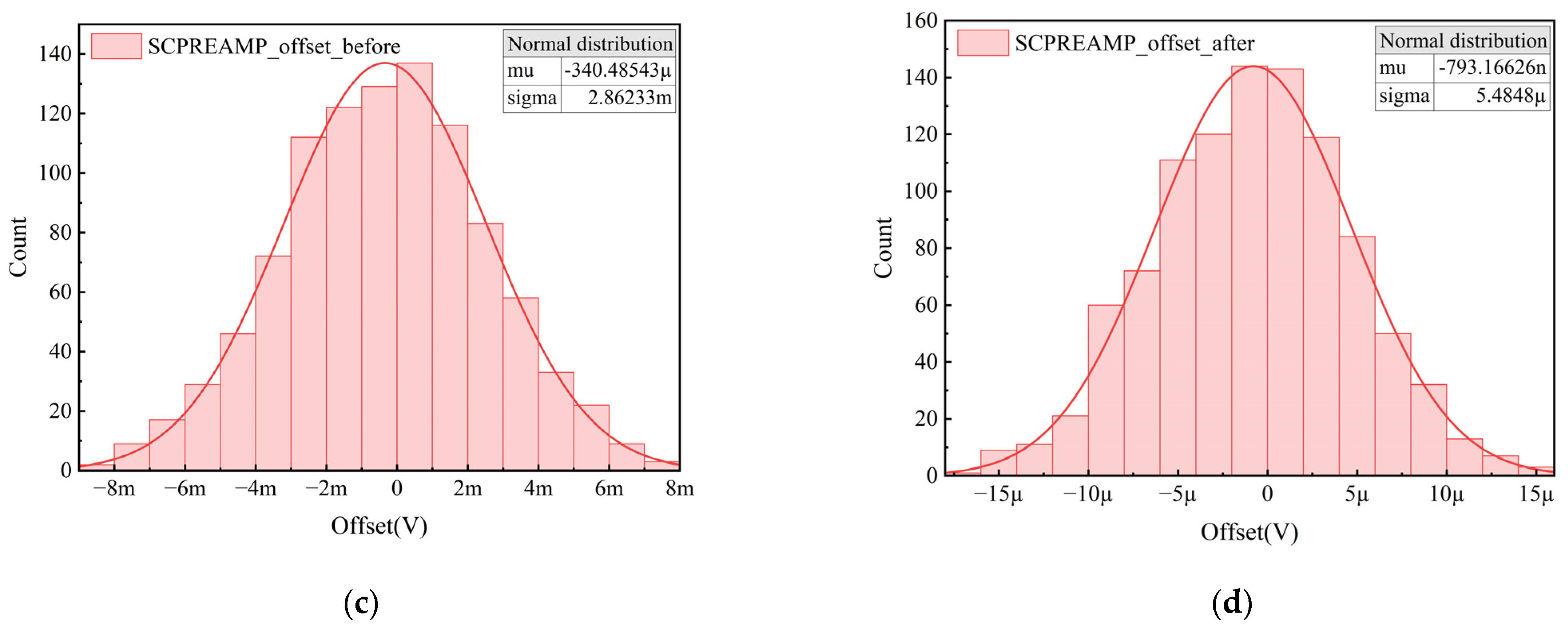
3.1. High-Precision Signal Processing Path

As shown in Figure 4, it is the analog signal path of the interface circuit. The key factors affecting comparison accuracy in this analog signal path are the offset and noise of the instrumentation amplifier, the offset of the switched capacitor amplifier, and the offset of the comparator. Therefore, this paper combines chopper stabilization and output offset storage technology [14,15,16,17,18] to achieve full signal chain offset and noise suppression, thereby achieving high-precision switch detection.
As shown in Figure 4, to eliminate the offset and noise of the instrumentation amplifier, the chopper instrumentation amplifier structure is used. The chopper amplifier consists of two chopper switches and an instrumentation amplifier. The instrumentation amplifier employs two identical CMOS operational amplifiers to form a dual-terminal in-phase amplification structure, as illustrated in Figure 4. This configuration effectively isolates the input signal source while delivering high input impedance. By precisely adjusting the resistor ratio, the instrumentation amplifier maintains a stable closed-loop gain. The chopper switch structure is illustrated in Figure 5. During the high phase of the control clock CLK, switches S1 and S2 are activated to conduct current, V O P = V I P and V O N = V I N . Conversely, when CLK transitions to its low phase, conduction is transferred to switches S3 and S4, V O P = V I N and V O N = V I P .
The ideal voltage waveforms at different circuit nodes of the chopper amplifier [19] are depicted in Figure 6. The first chopper modulates the input signal to a higher frequency. Then, the amplifier amplifies the modulated signal superposed on its own input offset, V o s 1 . Lastly, the second chopper demodulates the amplified input signal and modulates the output offset of the instrumentation amplifier. An output signal with an offset ripple and no DC offset is obtained at point D. Since global chopping technology is used, the output formulas in the two phases of the chopping sequence are as follows:
V o 1 = A ( V I P V I N ) + A V o s 1
V o 2 = A ( V I P V I N ) A V o s 1
where V o 1 is the differential output of the chopper amplifier when the chopper clock is high, V o 2 is the differential output when the chopper clock is low, and A is the closed-loop gain of the chopper amplifier.
To eliminate the output offset ripple of the chopper amplifier, the fully differential switched capacitor amplifier architecture [20] is adopted in this paper. Its simplified model is shown in Figure 7. The switched-capacitor amplifier adopts bottom plate sampling technology to eliminate the influence of parasitic capacitance. In addition, the switched capacitor amplifier has six inputs, which sample the differential switch threshold voltage and the output of the instrumentation amplifier at different phases of the chopper clock. These inputs perform addition and subtraction operations on the voltages, thereby eliminating the output offset ripple of the chopper amplifier and subtracting the switch transition threshold from the input signal.
As shown in Figure 8, the schematic diagram illustrates the relationship between the sampling timing and the chopping timing. When the switched-capacitor amplifier is in the φ 1 phase, switches S1 and S6 are closed, while S2, S3, S4, and S5 are disconnected, placing the amplifier in a reset state. In the φ 2 phase, switches S2 and S6 are closed, while S1, S3, S4, and S5 are disconnected, allowing the amplifier to sample the output voltage of the chopper amplifier, V o 1 , as shown in Formula (1). In the φ 3 phase, switches S2, S3, and S6 are closed, while S1, S4, and S5 are disconnected, placing the amplifier in a reset state again. In the φ 4 phase, switches S2, S4, and S5 are closed, while S1, S3, and S6 are disconnected, enabling the amplifier to sample the output voltage of the chopper amplifier, V o 2 , as shown in Formula (2), along with the switch threshold voltage V T . Then, through charge sharing, the addition and subtraction operations of the three are realized and output.
Therefore, the fully differential switched capacitor amplifier output formula is as follows (in this design, C 2 = 2 C 1 ):
V o = 0.5 [ V o 1 + V o 2 2 V T ] + V o s 2
where V o s 2 is the offset voltage of the main op-amp of the switched-capacitor amplifier.
Since the output offset voltage of the switched capacitor amplifier is the same in both the sampling phase φ 1 3 and the amplification phase φ 4 , the offset of the main op-amp of the switched capacitor amplifier can be regarded as the input offset of the next stage circuit. Additionally, since the output voltage of the switched capacitor amplifier exhibits a discrete time signal characteristic, as shown in Figure 4, the comparator adopts the architecture of the pre-amplifier and dynamic comparator [21] and employs output offset storage technology to eliminate both the offset of the pre-amplifier and the offset of the main op-amp.
As shown in Figure 9, V o s 4 = V o s 3 + V o s 2 , where V o s 3 is the original offset voltage of the pre-amplifier. The comparator works in two phases, namely the offset storage phase and the amplification phase. In the offset storage phase, the switch S is closed, the output offset of the pre-amplifier is stored on the capacitor, and the voltage difference across the capacitor C is:
V C = V r e f V c m + A p r e V o s 4
where A p r e is the gain of the pre-amplifier, V c m is the output common mode voltage of the pre-amplifier, and V r e f is a reference voltage.
When the comparator is in the amplification phase, switch S is turned off. The input signal after pre-amplification is minus the output offset voltage of the pre-amplifier. The final differential output voltage formula of the pre-amplifier is as follows:
V = A p r e ( A ( V I P V I N ) V T )
The specific implementation circuit diagram of the comparator is shown in Figure 10. The pre-amplifier uses a diode-connected MOSFET as a load and operates in an open-loop amplification state. Its open-loop gain is 20.29 dB and the −3 dB bandwidth is 4.14 MHz. Since the dynamic comparator is reset during the offset storage phase, an SR latch is added to latch the comparison result in the amplification phase.
As shown in Figure 11, it is the Monte Carlo simulation result of the combined offset voltage of the switched capacitor amplifier and the pre-amplifier and the offset voltage of the chopper amplifier.

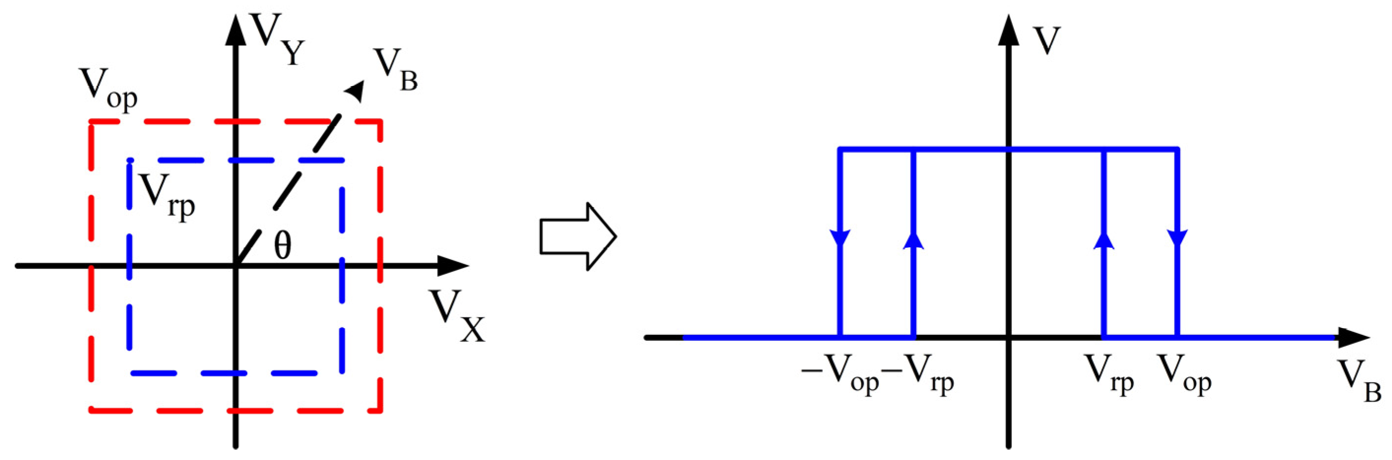
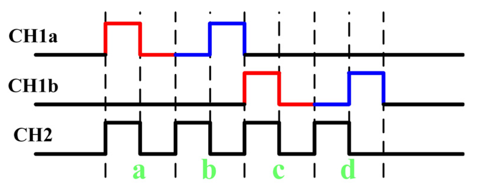
3.2. Switch Signal Algorithm

As shown in Figure 12, the schematic diagram illustrates the switch signal generation logic. Figure 13 shows the corresponding chopper switch clock control timing. By using the chopper switch in Figure 12 and the control timing in Figure 13, the input switching and input polarity switching functions of the 1D magnetic sensor element in the X and Y directions are realized. Therefore, in the four chopping cycles (a, b, c, and d), four comparison results (A, B, C, and D) are obtained, which respectively represent the four comparison results between the output signal of the 1D magnetic induction element in the X direction, the output signal in the X direction after polarity reversal, the output signal of the 1D magnetic induction element in the Y direction, and the output signal in the Y direction after polarity reversal and the set switching threshold. These results are input into the switching signal algorithm module and stored by four D flip-flops, respectively, as shown in Figure 14. Then, the final digital switch signal is obtained through the combinational logic in the following formula:
S W o u t = ( A B ) ( C D )
This combinational logic realizes that, when any one of the four comparison results is low, the 2D magnetic switch interface circuit outputs a low level, which represents that the input signal exceeds the threshold, thereby realizing the full polarity threshold judgment of the 2D magnetic field at a low cost. Additionally, by using X O R logic instead of A N D logic, false triggering of the switch caused by the comparison results of A and B or C and D being simultaneous is prevented, thereby enhancing the robustness of the circuit.

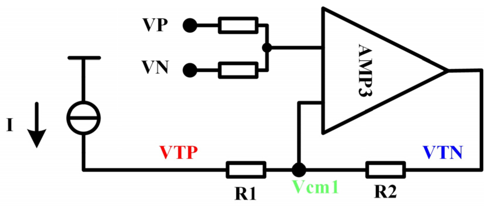
3.3. Switching Threshold and Hysteresis Range Design

The magnetic switch transition threshold generation circuit is illustrated in Figure 15. Here, V P and V N are the outputs of the chopper amplifier. The equivalent switch threshold formula at the input of the 2D magnetic switch interface circuit is as follows ( R 1 = R 2 = R ):
V T = 2 I R / A
In this design, the switching threshold is adjusted by varying the current, I . To enhance the versatility of the interface circuit, a 4-bit trim code is implemented to adjust the threshold. Additionally, if hysteresis needs to be set, it can be achieved by externally connecting the interface circuit’s output pin, S W o u t , to one of the trim code pins. Since a low level on S W o u t indicates that the input signal exceeds the threshold, this connection allows the hysteresis interval to be configured. The final switch threshold formula of the 2D magnetic switch interface circuit is as follows:
V o p = 2 ( 2 3 B i t 3 + 2 2 B i t 2 + 2 1 B i t 1 + 2 0 B i t 0 ) I 0 R / A
V r p = 2 ( 2 3 B i t 3 + 2 2 B i t 2 + 2 1 B i t 1 + 2 0 B i t 0 2 x B i t x ) I 0 R / A
where V o p is the operating point voltage of the switching threshold, V r p is the release point voltage of the switching threshold, B i t 3 0 represents the input code of the 4-bit trim code, B i t x is the bit represented by the trim code to which the output of the 2D magnetic switch interface circuit is connected, and I 0 is the unit current value of the current source.
Therefore, by incorporating a 4-bit trim code, the switching transition threshold and hysteresis range can be flexibly configured to adapt to various application fields and requirements, greatly enhancing the versatility of the 2D magnetic switch interface circuit.

3.4. Sleep and Wake-Up Mode

This low-power 2D integrated magnetic switch signal processing chip is designed by using clock-controlled micro-power technology. The clock logic circuit inside the chip enables the chip to sample external input signals at a frequency of 20 Hz. There are two working states in one cycle: awake state and sleep state. In the awake state, the output voltages of the two 1D magnetic sensor elements are sampled, and the chip works with a fast clock. After 9.5 fast clock cycles, the chip enters sleep mode. In sleep mode, the power consumption of the chip is almost negligible, as shown in Figure 16. And Figure 17 shows the breakdown of power consumption. In the awake state, all modules of the chip are operational, resulting in a current consumption of 2.432 mA. In the sleep state, only the 20 Hz low-speed oscillator and digital output driver remain active, reducing the chip’s power consumption to 3.989 μA. During the 50 ms detection cycle, the chip remains active for only 57 μs and spends the remainder of the cycle in sleep state. This approach has reduced the chip’s average current consumption from 2.432 mA to 6.757 μA while ensuring proper operation of the 2D integrated magnetic switch interface circuit.

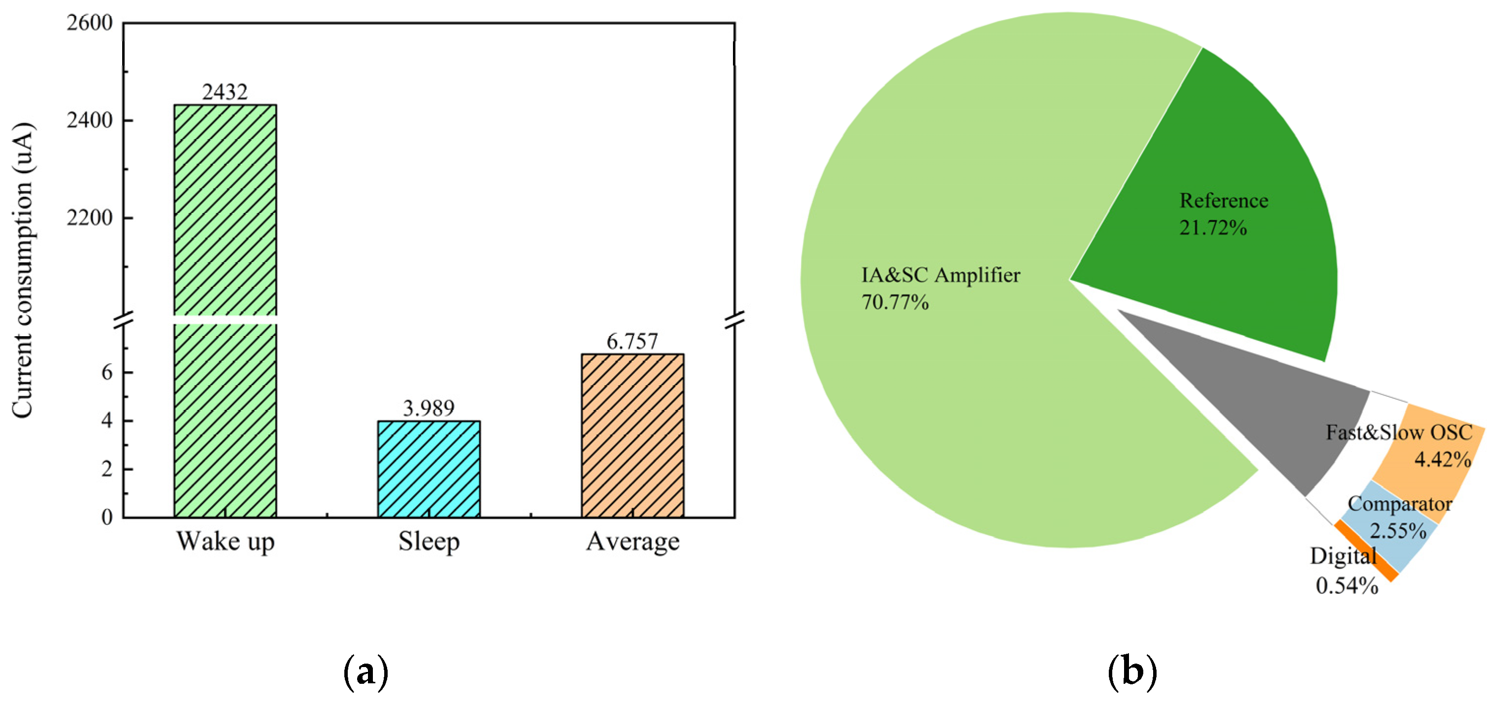
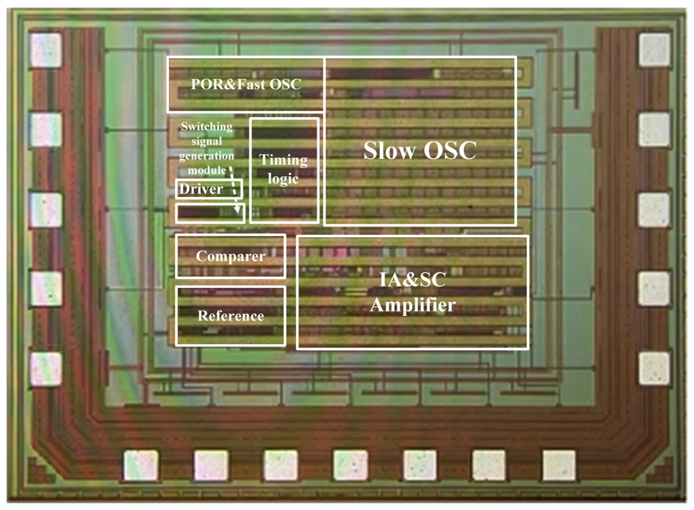
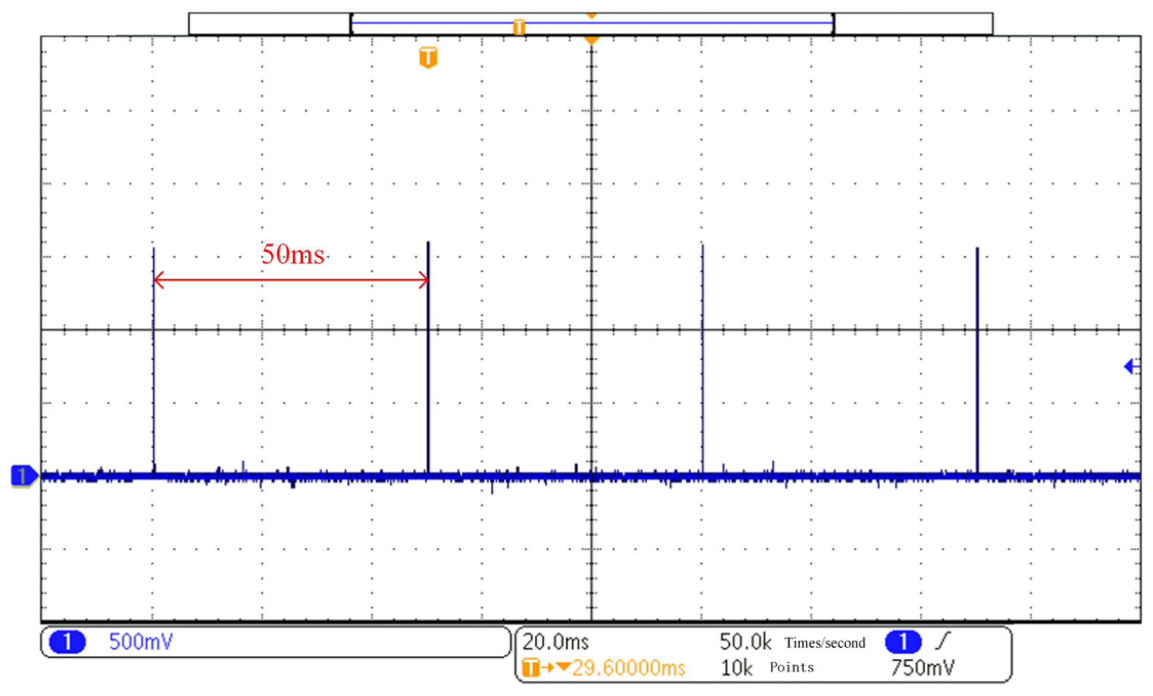
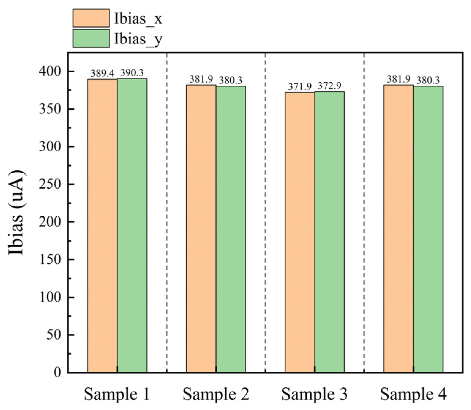
4. Results and Analysis

The chip has been fabricated in 0.18 um BCD technology with an area of 1.18 mm 2 . And, to reduce the impact of mechanical stress on the 2D magnetic switch interface circuit chip during the packaging process, the chip is packaged in bare chip COB (Chips on Board) [22]. The microscope photo of the chip is shown in Figure 18.
In this design, the bias of the two 1D magnetic sensing elements is supplied by the interface circuit and is only provided in the wake-up mode to minimize power consumption. Therefore, the slow clock working cycle can be obtained by measuring the bias pin voltage. As shown in Figure 19, the measurement results indicate that the detection frequency is 20 Hz. And Figure 20 shows the output bias current of four samples.
The input–output relationship measurement result of the chip is shown in Figure 21. In this photograph, the two triangular wave signals serve as positive inputs along the X and Y axes, respectively, while their corresponding negative inputs are biased at the common-mode voltage. The bottom digital signal is the 5 V CMOS digital output signal of the interface circuit. The diagram demonstrates that switching activation occurs when either directional input signal surpasses its predetermined threshold level. This operational characteristic effectively illustrates the chip’s capability for two-dimensional full-polarity detection.
To enhance the versatility of the 2D magnetic switch interface circuit to adapt to different application scenarios, a 4-bit trim code is designed to configure the chip’s jump threshold and hysteresis interval. Since the two 1D magnetic sensing elements share a set of interface circuits, one group is given a differential triangle wave signal, while the other group is given a common mode signal during measuring. To accurately measure the chip’s jump threshold under different codes, the hysteresis interval size is set to 0 during the measurement (that is, the chip output is not connected to any trim code pin). The measurement results of the chip under different trim codes are shown in Figure 22. These results demonstrate that the switch jump threshold can be adjusted within the range of 0 to 13.52 mV and the hysteresis threshold can be adjusted within the range of 0 to 7.32 mV through trim. In addition, the gain error in Figure 22 is mainly caused by the switch transition threshold voltage in the circuit being greatly affected by the process and has nothing to do with the high-precision signal chain.
The performance of the proposed interface circuit is summarized and compared with other magnetic switch interface circuits in Table 2. Compared with reference [12], this circuit not only realizes multi-dimensional detection but also slightly reduces the average current consumption. Although reference [10] realizes three-dimensional detection, on the one hand, its average current consumption is particularly large, and, on the other hand, its three-dimensional detection results are independent of each other, requiring additional signal processing. Reference [13] can only perform one-dimensional magnetic field detection, and the switching threshold is very large and is not suitable for high-precision detection scenarios. None of these three references give the specific offset size, so no comparison is made here. Finally, none of the three can adjust the switching threshold, so this design is slightly better in flexibility and practicality.

5. Conclusions

This paper uses the 180 nm BCD process to design a 2D integrated magnetic switch interface circuit. Chopper technology and output offset storage technology are used to effectively suppress the offset voltage of the interface circuit, improve the performance of the interface circuit, and achieve extremely low offset. Furthermore, by combining the physical circuit and the algorithm, the 2D omnidirectional and omnipolar switch detection function is realized. At the same time, sequential logic is employed to regularly control the chip’s sleep and wake-up cycles, thereby reducing average current consumption from 2.432 mA to 6.757 μA. Finally, the off-chip trim method is used to realize the flexible configuration of the switching threshold and hysteresis interval of the interface circuit to adapt to different application scenarios and enhance the versatility of the interface circuit.

Author Contributions

Conceptualization, Y.X. and Y.L.; formal analysis, Y.Z.; investigation, Y.X.; project administration, Y.L. and Y.Z.; resources, Y.Z. and Y.L.; data curation, Y.X. and Q.Z.; supervision, Y.Z. and Y.L.; visualization, Y.X. and Q.Z.; writing manuscript, Y.L. and Y.X.; review and editing, Y.X., Y.L. and Y.Z. All authors have read and agreed to the published version of the manuscript.

Funding

This research received no external funding.

Data Availability Statement

Data are contained within the article.

Conflicts of Interest

The authors declare no conflicts of interest.

References

  1. Gerard, C.M.; Meijer, M.S. Smart Sensor System; Antony Rowe Ltd.: Chippenham, UK, 2008; pp. 1–21. [Google Scholar]
  2. Chen, X.; Liu, J.; Tang, Y.; Lin, S. A monolithic CMOS Hall switch sensor system with high precision and low power consumption. In Proceedings of the 2019 6th International Conference on Electrical and Electronics Engineering (ICEEE), Istanbul, Turkey, 16–17 April 2019. [Google Scholar]
  3. Zhang, S.; Liu, S.; Yuan, C.; Duan, N. Design of the CMOS switching hall sensor circuit. In Proceedings of the 2018 International Conference on Sensor Networks and Signal Processing (SNSP), Xi’an, China, 28–31 October 2018. [Google Scholar]
  4. Zhu, H.C.; Qian, Z.H.; Huang, X.W. Integrated GMR magnetic switch for implantable medical devices. In Proceedings of the 2010 Asia Pacific Conference on Postgraduate Research in Microelectronics and Electronics (PrimeAsia), Shanghai, China, 22–24 September 2010. [Google Scholar]
  5. Wu, R.; Kofi, A.A.; Johan, H.H. A chopper current-feedback instrumentation amplifier with a 1m Hz 1/f noise corner and an AC-coupled ripple reduction loop. IEEE J. Solid-State Circuits 2009, 44, 3232–3243. [Google Scholar] [CrossRef]
  6. Johan, F.W.; Kofi, A.A.; Johan, H.H. Dynamic Offset Compensated CMOS Amplifiers; Springer: Berlin/Heidelberg, Germany, 2009; pp. 43–64. [Google Scholar]
  7. Ronis, N.; Mariano, G.I. Design and characterization of Hall Plates in a 0.5 um CMOS process. In Proceedings of the 2016 Argentine Conference of Micro-Nanoelectronics, Technology and Applications (CAMTA), Neuquen, Argentina, 4–5 August 2016. [Google Scholar]
  8. Popovic, R.S. Hall Effect Devices, 2nd ed.; CRC Press: Boca Raton, FL, USA, 2003; pp. 30–49. [Google Scholar]
  9. Asahi Kasei Microdevices. Available online: https://www.akm.com/global/en/products/hall-sensor/hall-element/ (accessed on 15 March 2025).
  10. Guo, S.Z. Integrated three-dimensional Hall switch sensor based on independent optimized Hall devices. Microelectron. J. 2023, 135, 105756. [Google Scholar]
  11. Yu, S.K.; Seong, I.C. A low noise Hall Effect Sensor Readout Circuit. IDEC J. Integr. Circuits Syst. 2019, 5, 16–21. [Google Scholar]
  12. Wei, R.S.; Guo, S.Z.; Yang, S.Z. Low-Power CMOS Integrated Hall Switch Sensor. Act. Passive Electron. Compon. 2017, 1, 5375619. [Google Scholar] [CrossRef]
  13. Zhu, H.C.; Qian, Z.H.; Bai, R.; Li, J.P. The Omnipolar Integrated Magnetic Switch Based on GMR. Key Eng. Mater. 2013, 562, 1234–1237. [Google Scholar] [CrossRef]
  14. Wu, R.; Johan, H.H.; Kofi, A.A. Precision Instrumentation Amplifiers and Read-Out Integrated Circuits; Springer: Berlin/Heidelberg, Germany, 2013; pp. 128–213. [Google Scholar]
  15. Fan, Q.W.; Kofi, A.A.; Johan, H.H. Capacitively-Coupled Chopper Amplifiers; Springer: Berlin/Heidelberg, Germany, 2013; pp. 106–154. [Google Scholar]
  16. Lin, T.N.; Wang, B.; Amine, B. Analysis of output ripple shape and amplitude in chopper instrumentation amplifier. IEEE Trans. Circuits Syst. II Express Briefs 2021, 69, 299–303. [Google Scholar] [CrossRef]
  17. Christian, C.E.; Gabor, C.T. Circuit techniques for reducing the effects of op-amp imperfections: Autozeroing, correlated double sampling, and chopper stabilization. Proc. IEEE 1996, 84, 1584–1614. [Google Scholar]
  18. Mountrichas, L.; Siskos, S. A novel switching scheme for offset storage cancellation technique, for GS/s range ADCS. In Proceedings of the 2012 IEEE International Instrumentation and Measurement Technology Conference Proceedings, Graz, Austria, 13–16 May 2012. [Google Scholar]
  19. Jiang, J.; Kofi, A.A. A multi-path CMOS Hall sensor with integrated ripple reduction loops. In Proceedings of the 2015 IEEE Asian Solid-State Circuits Conference (A-SSCC), Xiamen, China, 9–11 November 2015. [Google Scholar]
  20. Razavi, R. Design of Analog CMOS Integrated Circuit, 2nd ed.; McGraw-Hill Education: New York, NY, USA, 2017; pp. 503–507. [Google Scholar]
  21. Allen, P.E. CMOS Analog Circuit Design, 3rd ed.; Oxford University Press: New York, NY, USA, 2012; pp. 488–492. [Google Scholar]
  22. Lau, J.H. Chip on Board: Technology for Multichip Modules; Chapman & Hall: New York, NY, USA, 1994; pp. 57–65. [Google Scholar]
Figure 1. (a) Practical application of two-dimensional magnetic switch chip; (b) diagram of magnetic field vector decomposition.
Electronics 14 01299 g001
Figure 2. Diagram of two-dimensional switch threshold and input and output relationship of full polarity detection.
Electronics 14 01299 g002
Figure 3. Architecture of proposed 2D integrated magnetic switch interface circuit.
Electronics 14 01299 g003
Figure 4. Analog signal path of the interface circuit.
Electronics 14 01299 g004
Figure 5. Structure of the chopper switch.
Electronics 14 01299 g005
Figure 6. Voltage waveforms at different circuit nodes of the chopper amplifier.
Electronics 14 01299 g006
Figure 7. The simplified circuit of the switched capacitor amplifier.
Electronics 14 01299 g007
Figure 8. The relationship between the sampling timing and the chopping timing.
Electronics 14 01299 g008
Figure 9. Schematic diagram of the comparator.
Electronics 14 01299 g009
Figure 10. The implementation circuit diagram of the comparator.
Electronics 14 01299 g010
Figure 11. Comparison of simulation results before and after using offset suppression technology: (a,b) the combined offset of the switched capacitor amplifier; (c,d) the offset of the chopper amplifier.
Electronics 14 01299 g011aElectronics 14 01299 g011b
Figure 12. Diagram of the switch signal generation logic.
Electronics 14 01299 g012
Figure 13. Chopper switch clock control timing.
Electronics 14 01299 g013
Figure 14. (a) Switch signal generation logic circuit; (b) the corresponding timing of the logic circuit.
Electronics 14 01299 g014
Figure 15. Magnetic switch transition threshold generation circuit.
Electronics 14 01299 g015
Figure 16. Low-power clock control sequence.
Electronics 14 01299 g016
Figure 17. Breakdown of power consumption: (a) current consumption under different working conditions; (b) power consumption ratio of different modules in the wake-up working state.
Electronics 14 01299 g017
Figure 18. Microscope photo of the chip.
Electronics 14 01299 g018
Figure 19. Measurement results for the detection frequency.
Electronics 14 01299 g019
Figure 20. The output bias current of four samples.
Electronics 14 01299 g020
Figure 21. Input–output relationship measurement result of this chip (trim code B3-B0 = 1111).
Electronics 14 01299 g021
Figure 22. Switching threshold measurement results of trim code scan.
Electronics 14 01299 g022
Table 1. Comparison of magnetic sensing elements.
Magnetic Sensor ElementSensitivity (mV/(V×mT))Output Voltage of 10 mT (mV)
GaAs Hall element [9]0.183–0.3671.83–3.67
InAs Hall element [9]0.6–0.9676–9.67
InSb Hall element [9]0.82–7.48.2–74
Silicon-based Hall element [7]0.03–0.04080.3–0.408
AMR 11–1010–100
1 anisotropic magnetoresistance.
Table 2. Comparison of the magnetic switch interface circuit.
Parameters[12][10][13]This Work
Process (μm)0.180.180.50.18/BCD
Chip   area   ( mm 2 )0.3961.46NA1.18
Supply voltage (V)3.33.355
Operating point voltage (mV)0.410.4140.5–55.350–13.52
Release point voltage (mV)0.260.2827–36.90–13.52
Hysteresis voltage (mV)0.150.133.6–28.350–7.32
Operating frequency (Hz)20NANA20
Average current consumption (μA)7.89>14.85NA6.757
Trim code (bit)0004
Dimensions1312
Disclaimer/Publisher’s Note: The statements, opinions and data contained in all publications are solely those of the individual author(s) and contributor(s) and not of MDPI and/or the editor(s). MDPI and/or the editor(s) disclaim responsibility for any injury to people or property resulting from any ideas, methods, instructions or products referred to in the content.

