Article

Machine Learning-Assisted Design and Optimization of a Broadband, Low-Loss Adiabatic Optical Switch

by
Mohamed Mammeri
1,*,
Maurizio Casalino
2,
Teresa Crisci
1,
Babak Hashemi
3,
Stefano Vergari
4,
Lakhdar Dehimi
5 and
Francesco Giuseppe Dellacorte
1
1
Department of Electrical Engineering and Information Technologies (DIETI), Università degli Studi di Napoli Federico II, 80125 Napoli, Italy
2
Istituto di Scienze Applicate e Sistemi Intelligenti (ISASI), National Research Council, Via P. Castellino 111, 80131 Napoli, Italy
3
Department of Information Engineering, Infrastructures and Sustainable Energy (DIIES), “Mediterranea” University, 89124 Reggio Calabria, Italy
4
Open Fiber S.p.A., Via Laurentina 449, 00142 Roma, Italy
5
Laboratory for Physico-Chemical Studies of Materials (LEPCM), University Batna 1, Elhadj-Lakhdar, Batna 05000, Algeria
*
Author to whom correspondence should be addressed.
Electronics 2025, 14(7), 1276; https://doi.org/10.3390/electronics14071276
Submission received: 25 February 2025 / Revised: 16 March 2025 / Accepted: 18 March 2025 / Published: 24 March 2025
(This article belongs to the Special Issue Advanced Photonic Devices and Applications in Optical Communications)

Abstract

:
The demand for faster and more efficient optical communication systems has driven significant advancements in integrated photonic technologies, with optical switches playing a pivotal role in high-speed, low-latency data transmission. In this work, we introduce a novel design for an adiabatic optical switch based on the thermo-optic effect using silicon-on-insulator (SOI) technology. The approach relies on slow optical signal evolution, minimizing power dissipation and addressing challenges of traditional optical switches. Machine learning (ML) techniques were employed to optimize waveguide designs, ensuring polarization-independent (PI) and single-mode (SM) conditions. The proposed design achieves low-loss and high-performance operation across a broad wavelength range (1500–1600 nm). We demonstrate the effectiveness of a Y-junction adiabatic switch, with a tapered waveguide structure, and further enhance its performance by employing thermo-optic effects in hydrogenated amorphous silicon (a-Si:H). Our simulations reveal high extinction ratios (ERs) exceeding 30 dB for TE mode and 15 dB for TM mode, alongside significant improvements in coupling efficiency and reduced insertion loss. This design offers a promising solution for integrating efficient, low-energy optical switches into large-scale photonic circuits, making it suitable for next-generation communication and high-performance computing systems.

1. Introduction

The increasing demand for faster, more efficient optical communication systems has driven significant research toward advanced integrated photonic technologies, which are crucial for integrating, manipulating, and processing optical signals alongside or in conjunction with electronic signals [1,2]. In particular, optical switches enable high-speed, low-latency data transmission by managing the routing of optical signals directly, without requiring conversion to electrical signals [3,4].
Optical switches are essential components in modern communication and computing systems, offering rapid switching and data transmission while eliminating the delays and energy losses associated with optical-to-electrical (O/E) and electrical-to-optical (E/O) conversions. This significantly reduces energy consumption and maintains signal integrity over long distances, avoiding noise and interference commonly associated with electrical systems [5,6]. These features make the optical switches ideal for data centers and telecom networks aiming to minimize their energy consumption and enhance real-time communication and high-performance computing applications.
Optical switches typically rely on carrier dispersion or thermo-optic effects to alter the material’s refractive index, enabling reconfigurable signal routing [5,7]. In general, bandwidth, extinction ratio, power consumption, insertion loss, and footprint are the main factors for most of the practical applications of photonic switches. However, different applications require different values of these factors [5]. Various types of silicon-integrated optical switches have been explored, primarily including the micro-ring resonator (MRR) [8,9], the Mach–Zehnder interferometer (MZI) [8,10], multimode interference structures (MMI) [11], and the hybrid type that combines both MRR and MZI structures [12]. Nevertheless, the limitations of these types of devices in a wide range of applications occur mainly due to the wavelength selectivity and the polarization sensitivity, which can limit the flexibility of multi-wavelength applications and increase the losses for certain wavelengths, making it difficult to ensure consistent performance [13].
In this work, we present a novel approach built on the principle of adiabatic processes for designing an adiabatic optical switch based on the thermo-optic effect, where the system evolves slowly enough that the optical energy remains in its lowest energy state throughout the transition. This allows for highly efficient operation with minimal power dissipation, addressing one of the key challenges in traditional optical switches [14,15]. The adiabatic switch was designed based on silicon-on-insulator (SOI) technology. The use of different materials such as hydrogenated amorphous silicon (a-Si: H), along with optimized waveguide designs assisted with machine learning techniques, has allowed for achieving the desired slow evolution of the light signal, ensuring minimal signal degradation during the transition, which offers the potential to create a low-loss, single mode (SM), and polarization-independent (PI) optical switch while ensuring consistent performance over the broad wavelength range of 1500 nm to 1600 nm. The proposed device is well-suited for large-scale photonic circuits, providing a robust, energy-efficient solution for complex optical networks.

2. Materials and Methods

The initial design phase of the adiabatic switch, which is considered our device’s fundamental building block, begins with defining the waveguide’s type, properties, and cross-sectional dimensions. Most of the works in the state of the art target compact devices with minimum feature sizes, requiring expensive technological processes, such as e-beam or deep ultraviolet lithography. Furthermore, as the single mode (SM) fiber used in telecommunications, e.g., in passive optical networks (PON), typically has a 9 μm core [16], coupling to and from a waveguide with sub-micrometric dimensions requests the introduction of additional photonic elements which might result in increased complexity and reduced bandwidths. We designed the device for fabrication processes requiring larger waveguide sizes, specifically with cross-sectional dimension values (width and thickness) exceeding 1 µm. This constraint poses a significant challenge in device design, requiring careful optimization to maintain performance. Nevertheless, this places our device way above the foundries lithography resolution standard of deep ultra-violet (DUV) 248 nm, as indicated in [17,18], with high fabrication tolerance.
A relatively large cross-section lowers the mode attenuation and allows for much longer signal travel distance [19], but makes the design of SM waveguides—which are crucial for most practical applications—more critical. Moreover, for obtaining SM condition in strip and planar waveguides, the minimum feature size should be of the scale of several hundreds of nanometers, with a typical thickness ranging from 200 nm to 400 nm [20,21,22]. Therefore, we used a rib waveguide structure based on the silicon-on-insulator (SOI) technology, which can be larger than strip waveguides whilst maintaining the SM condition [23]. The cross-section is illustrated in Figure 1a, which consists of a raised rib structure obtained by etching out of a planar waveguide layer. The parameters of the cross-section include the width (W), the total height (H), the slab height (h), and the etching depth. The material used for the rib and slab is hydrogenated amorphous silicon (a-Si:H) with a refractive index of 3.478. The reason for using specifically this material will be discussed later. The whole structure is surrounded by a cladding layer of silicon dioxide (SiO2) with a refractive index of 1.444 and a thickness of 3 µm. The SOI platform also contains a 3 µm-thick SiO2 layer separating the slab from the silicon bulk substrate.

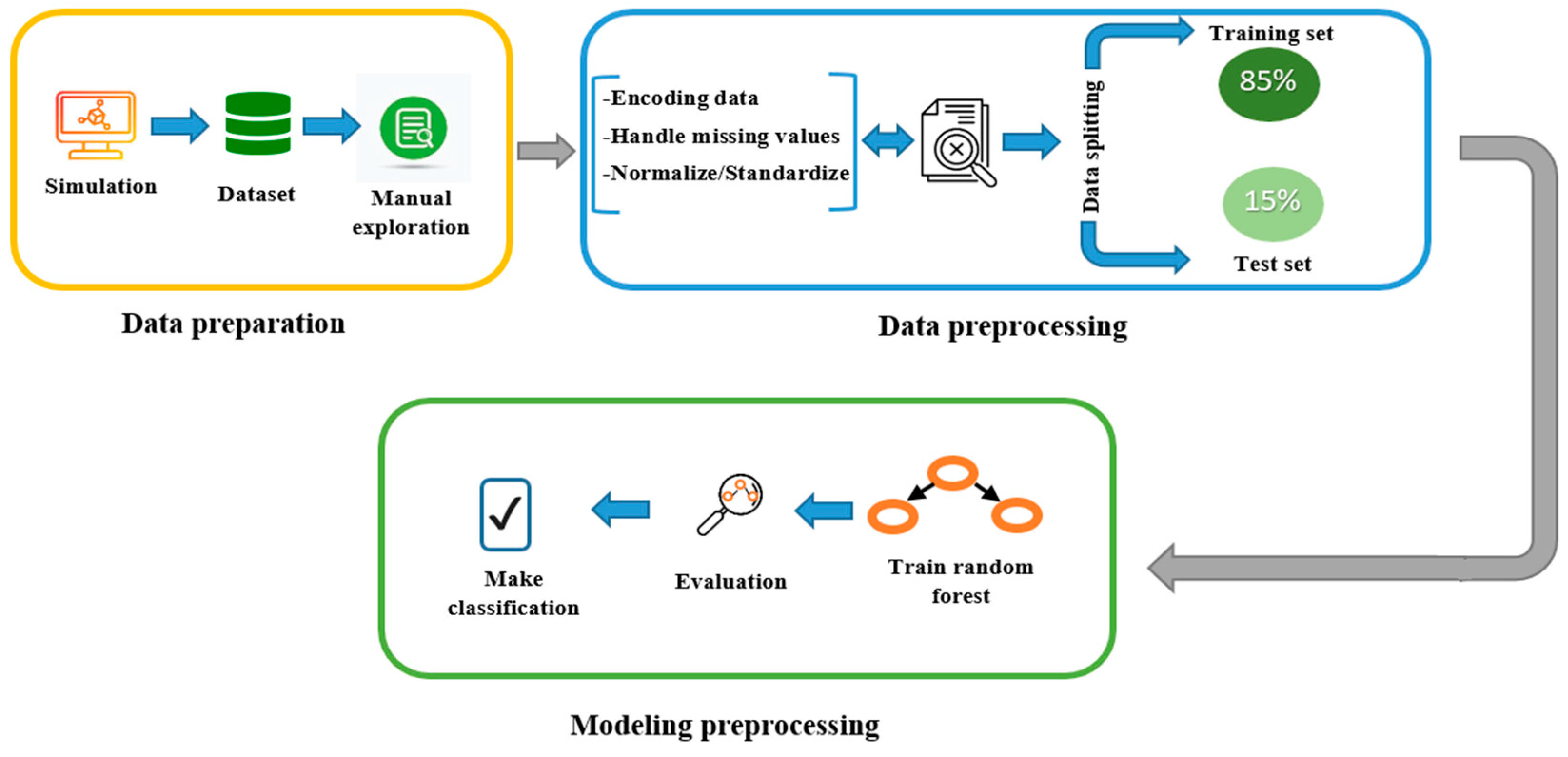
2.1. Machine Learning Technique Application

Many researchers have aimed to find easy and reliable methods for finding SM and polarization independence (PI) conditions for the rib waveguide. Petermann et al. introduced one of the earliest works for determining SM condition of the rib waveguide [24]. Based on Petermann’s work, Soref et al. provided a simple expression for large rib waveguides based upon their geometry, identifying the SM condition as follows [25,26]:
W H α + r 1 r 2     f o r   0.5 r 1.0
where r = h/H is the ratio of the slab height to the total waveguide thickness, and α is a constant optimized through modeling. Confining the value of r between 0.5 and 1, this formula constrains the waveguide to have a shallow-etched rib and does not consider the case of deep-etched waveguides. Similarly, by using the analytical effective index method, Pogossian et al. found that the geometrical constraints need to be more restricted [26]. However, obtaining the PI condition was demonstrated to be more difficult. W. R. Headley found that r should be less than 0.5 µm for a waveguide with a feature size of around 1 µm [23], which contravenes the SM condition. Therefore, in this work, we developed an ML-based approach to determine the optimal single-mode (SM) and polarization-independent (PI) conditions for rib waveguides. Our approach leverages the rapidity of the ML techniques and provides reliable results.

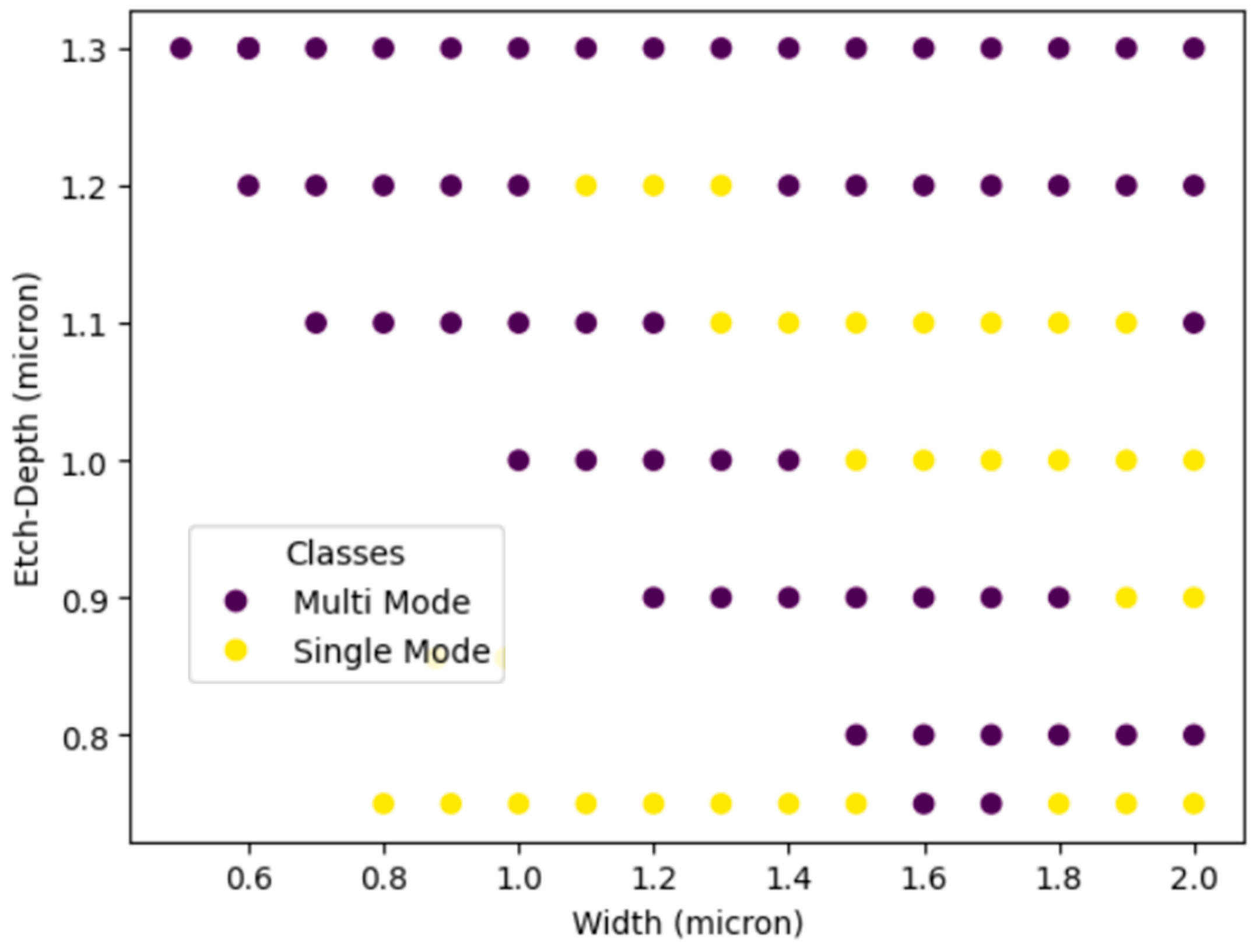
2.2. Dataset Construction

A dataset of thousands of rib waveguide geometries was generated by using Mode solver in the Lumerical simulation environment [27]. The use of computational data enables access to a larger amount of data compared to experimental data, which are also often expensive to obtain, although experimental data should be regarded as more reliable for device fabrication.
In the simulation process, W, H, and etch-depth were the three dimensions that were varied while recording the effective refractive index of rib and slab and the polarization of the propagated mode. Then, the SM was determined by comparing the effective index of the rib with that of the slab. If we found only one guided mode for each polarization, then we considered this waveguide as a SM waveguide and vice versa. In contrast, the waveguide was considered PI if the effective index was equivalent within an approximation of 10−3 for both polarization states, which made the fundamental TE and TM modes effectively propagate at the same velocity. To systematically identify the single-mode (SM) and polarization-independent (PI) conditions, we generated a comprehensive dataset of rib waveguide geometries through numerical simulations. In our dataset, a wide range of parameter values was considered to ensure comprehensive coverage of the design space. Specifically, both W and H ranged from 0.5 µm to 2 µm, with a step value of 0.1 µm, while the etch-depth range varied depending on the H value, while maintaining a minimum rib and slab thickness of 0.2 µm. This constraint was imposed to prevent the formation of fully planar or ridge waveguides, thereby preserving the intended waveguide geometry. The dataset consists of 3110 data points. A representative sample is presented in Table 1.

2.3. Machine Learning Model Building

Generally, building an ML model passes through several steps, as depicted in Figure 2. After collecting the data, it is first essential to conduct a pre-processing operation to prepare the data and render them suitable for the ML model training. The first step is encoding the columns that have categorical values (polarization and single mode columns—see Table 1) to numerical values to be usable by the model function. Then, the imputation process is important to handle missing values and corrupted data. After that, data standardization is required at the same scale, an operation enhancing the model performance.
Another step before training the model is to define the hyper-parameters that control the learning process, which requires choosing the optimal parameters. However, there is no specific way to determine the optimum hyper-parameters [28]. Rather, the common method consists of modifying the values of different parameters and repeating the experiment until the best results are obtained. Therefore, we used the GSCV algorithm for this purpose [29]. This algorithm processes a given set of parameters and tries every possible value, then uses an internal cross-validation technique to calculate the average score for each parameter combination. The bigger the score obtained, the better that combination of hyper-parameters. Herein, we used the Random Forest algorithm [30], with the following hyper-parameters: the number of trees in the forest is 20, the function to measure the quality of a split is ‘log loss’, the minimum number of samples required to be at a leaf node is 1, and the maximum depth of the tree is 10.
After a pre-processing step, the dataset was partitioned into two subsets, with 85% used for training the machine learning model and the remaining 15% reserved for evaluating its accuracy. In addition, we compared 450 data points classified by ML with the results of the simulation by using Lumerical to assess the accuracy of our model, reaching a 99% accuracy score for SM condition classification, and a 97.8% accuracy score for PI.
The results showed a large variety of cross-section dimensions for obtaining SM, as shown in Figure 3, although one should be aware that the boundaries of the yellow-dotted regions represent critical combinations for which a clear discrimination between SM and MM behavior is not possible, also in consideration of possible technological tolerances. Additionally, we took into consideration three other criteria, namely: (a) the waveguide should be polarization independent; (b) the width of the waveguide should be large enough to be able to design a tapered waveguide respecting our minimum feature size; and (c) the thickness should be 1.5 µm. The cross-section dimensions of the obtained waveguide are listed in Table 2. Compared to traditional iterative design approaches, the ML-based method significantly reduced computational time while maintaining accuracy.

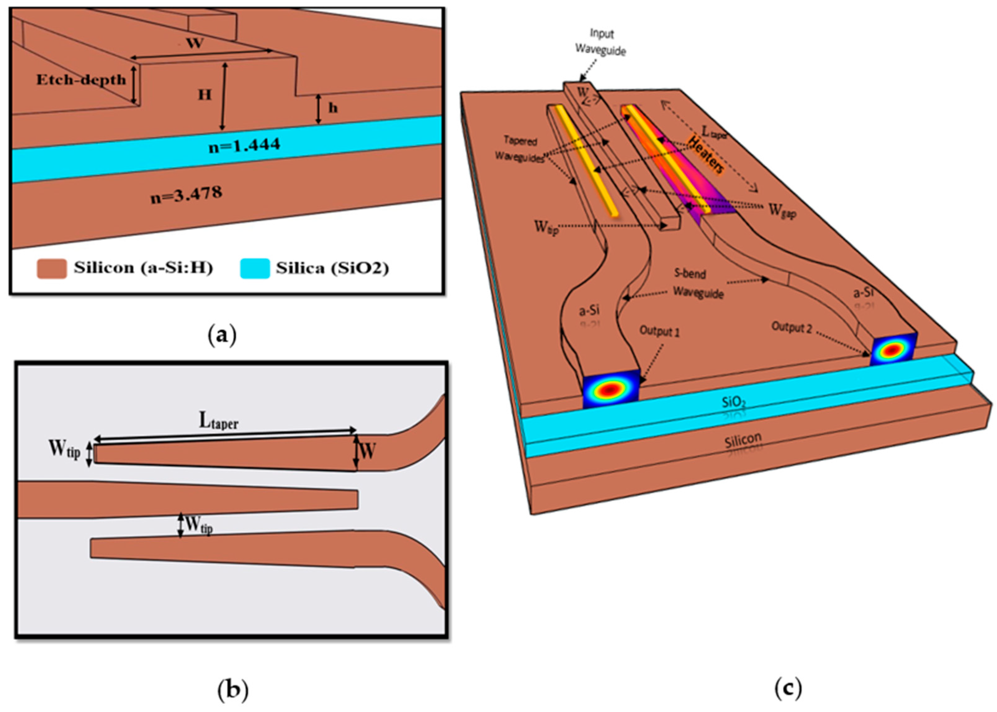
2.4. 1 × 2 Y-Junction Adiabatic Optical Power Splitter Design

The adiabatic switch design is based in fact on a Y-junction power splitter, consisting of one input and two output rib waveguides, three tapered rib waveguides, and two S-bend rib waveguides, as illustrated in Figure 1c. The slab is common to all of the waveguides. The cross-section geometries for SM and PI behavior, obtained from the ML process, are a rib etching depth of 750 nm, W of 1.4 µm, and H of 1.5 µm. The geometry of the device is summarized in Table 2.
The wider end of each tapered waveguide (W) is 1.4 µm, while the tip width (Wtip) is anticipated to have the minimum feature size of the design, which yields to a shorter coupling length with higher efficiency [31]. The central tapered waveguide width slowly decreases from 1.4 µm to 0.5 µm in the direction of light propagation; two tapered waveguides are formed symmetrically for the output ports with reverse tapering, where width slowly increases from 0.5 µm to 1.4 µm in the direction of the light propagation. This type of tapered waveguide is used to increase the mode connection power transfer efficiency [MCTE] by changing the shape and size of the optical mode [32], which causes a coupling/splitting of power from the input waveguide to the output waveguides adiabatically.
To investigate the effect of different Wtip and gaps (Wgap), the latter being the physical separation or spacing between adjacent waveguides in Figure 1b,c, we studied first a passive Y-adiabatic splitter with the same geometry and varying Wtip and Wgap using an EME (eigenmode expansion) solver. We studied in particular the fundamental TE mode, with a high effective index of 3.478 and low loss of 0.00117 dB/cm. Figure 4 shows the obtained power transmission as a function of the tapered waveguide length (Ltaper). The results show that theoretically, a high coupling coefficient of 98% with a 50:50 splitting ratio can be achieved for three different values of Wtip and Wgap. However, Ltaper is significantly reduced—in terms of obtaining a higher power transfer coefficient—with smaller Wtip, as shown in Figure 4a. Likewise, increasing the gap between tapers in the coupling region strongly reduces the power transfer, as shown in Figure 4b. Further discussion of these results will be provided in the next section.
Following the adiabatic coupling region illustrated in Figure 1b, the lateral tapers are separated using S-bent waveguides with a sufficient length to reduce the bend losses.

2.5. Setup of Thermo-Optic Effect Simulation for the Adiabatic Switch

The passive splitter discussed so far can be modified to allow light switching between its outputs by introducing a slight increment of the refractive index in one of the two tapered output waveguides. The effectiveness of this approach was demonstrated in a recent paper about a similar device, based however on a standard narrow ridge waveguide [33]. Hereafter we will similarly rely on the thermo-optic effect in a-Si:H, a photonic material which can be simply and reliably deposited and defined by etching just like its crystalline counterpart [34]. One drawback of the thermo-optic principle consists in the thermal crosstalk effect, which often restricts its use in integrated photonics due to the temperature variation affecting also the nearby regions and the elements of a composite device. However, this parasitic effect is strongly dependent on the device size and on the thermal conductivity of the materials they are made of. For this reason, we have investigated large cross-section waveguides and a-Si:H to reduce the thermal crosstalk, benefiting moreover from the low thermal conductivity of 1.5 W/mK of this semiconductor alloy, compared to that of crystalline Silicon (c-Si) (148 W/mK). Additionally, a-Si:H shows low optical absorption, which allows for low losses [35,36], while its refractive index can be slightly tuned by changing the amount of the hydrogen present in the alloy [37].
Steady-state thermal simulations were first initiated using Lumerical Heat solver to calculate the temperature distribution of the device. Two titanium (Ti) wire heaters were placed at a distance (h) of 0.5 µm above the lateral waveguides (Figure 1c and Figure 5b). At this distance, the heaters did not significantly affect the optical propagation due to the good confinement of modes in the center of the large cross-section waveguides. The thermal properties and the thermo-optic coefficients of the materials used in this simulation are summarized in Table 3.
The lateral boundary conditions were considered isothermal while there is heat transfer by convection between air and the exposed SiO2 cladding surface on top. Figure 5a illustrates the temperature values recorded the three waveguides at half length of the tapered region (Ltaper/2), in a power dissipation range of practical interest applied to the Ti heater corresponding to Output 2. The temperature values were recorded at half the height of the waveguides (see the temperature monitor in Figure 5b). The results show that the waveguide temperature was linearly dependent on the power applied to the Ti wire. Moreover, it can be seen that, at high power, there were significantly different temperatures between the two lateral waveguides. For a power range of 0.5 mW/µm to 0.7 mW/µm, the temperature difference between the lateral waveguides varied between 70 K to 115 K. The low thermal conductivity of a-Si:H, its relatively high heat capacity, and also the low thermal conductivity of SiO2 were in fact leveraged to minimize heat spreading to the other regions of the device.

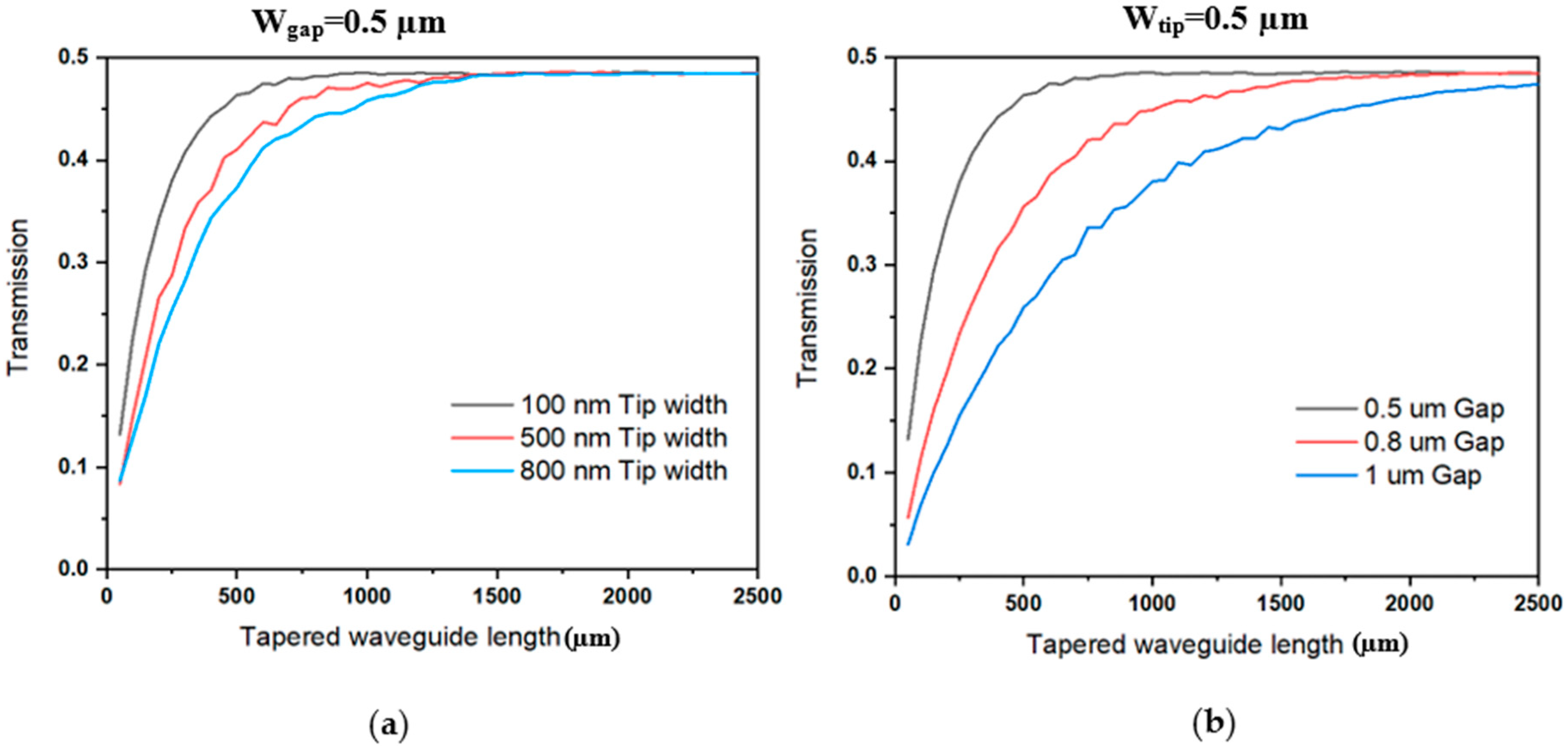
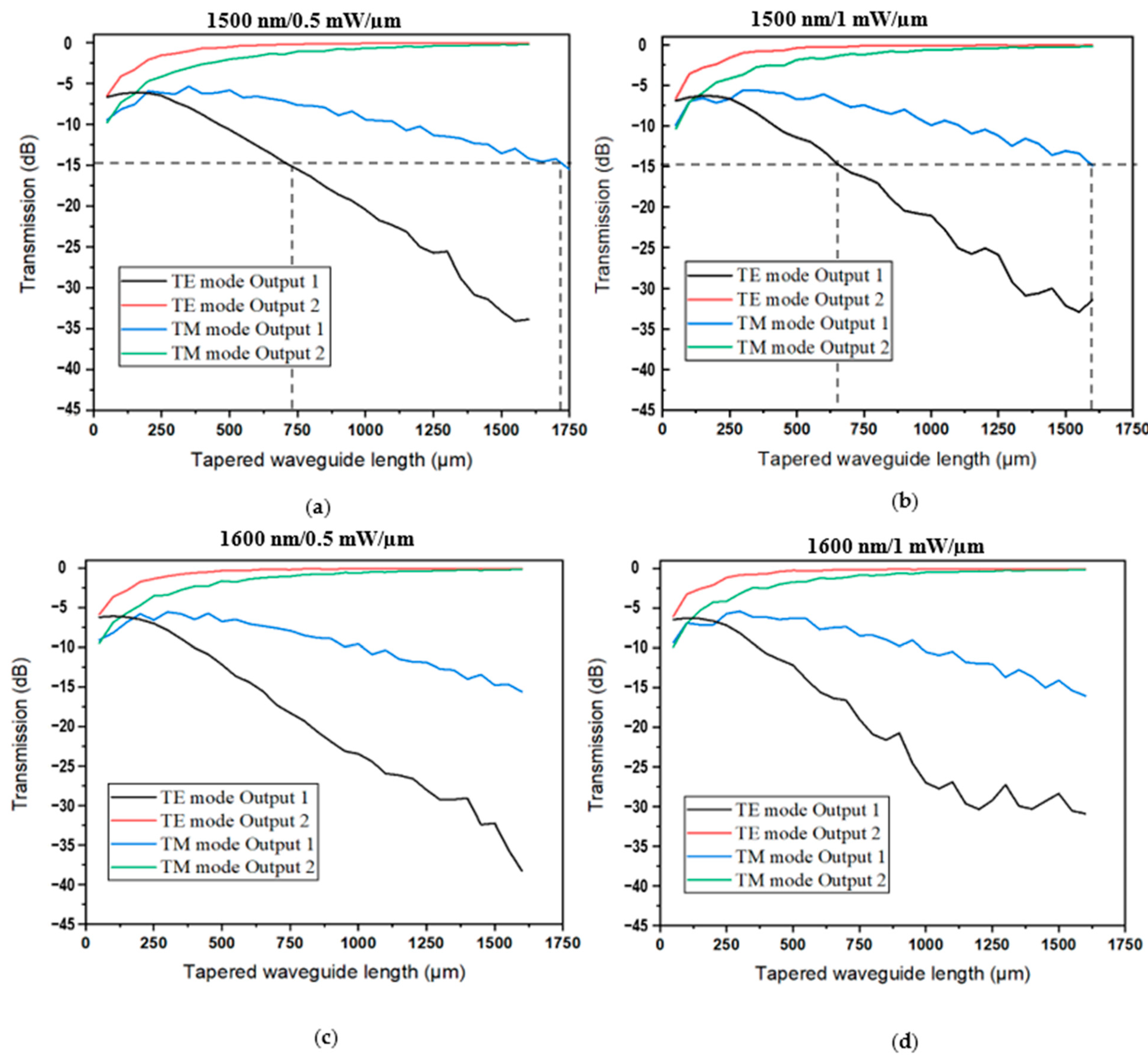
3. Y-Adiabatic Switch Optical Simulation

As a means to change the refractive index profile in the coupling regions of the adiabatic switch, we have used the thermo-optic effect. To this end, the temperature profiles obtained from previous simulations are used as an input for optical simulations, allowing us to calculate the related magnitude of the local change of the refractive index. To this end, we adopted experimental values of the thermo-optic coefficient (TOC). The TOC for a-Si:H at 1.55 µm was accurately measured in a wide temperature range in [39]. In particular, at room temperature:
d n d t = 2.3 × 10 4 K 1
This value was obtained in thick slab waveguides realized by Plasma Enhanced Chemical Vapor Deposition at 170 °C. The low deposition temperature favors the H2 incorporation, which in turn reduces the defect concentration and allows absorption coefficients as low as 0.05 cm−1 [43].
The calculated effective refractive index profile for the TE mode along the same cutline of Figure 5b,c is shown in Figure 6 (top graphs) for a dissipated power of 0.1, 0.5, and 1.0 mW/µm. Due to the polarization-independent design, the TE and TM modes exhibit nearly identical refractive index variations ( n T E T M 10 3 ).
By using these data, we have simulated the change in the optical power transmission at 1500 nm and 1600 nm wavelengths (λ). The results obtained are shown in Figure 7 for both TE and TM polarizations, for dissipated powers of 0.5 and 1.0 mW/µm. Here the y-axis represents the power transmission in dB, and the x-axis represents the coupling region length (Ltaper).
Figure 7 shows that adiabatic switches maintain high performance across a range of coupling lengths, unlike classical directional couplers that require precise critical lengths for optimal operation. The coupling length in a directional coupler is wavelength-dependent due to the differential material dispersion, where each optical wavelength propagates with its own velocity. Hence, this dispersion causes different coupling coefficients for different wavelengths and requires critical coupling lengths [44,45]. Alternatively, B. Hashemi et al. proved that the adiabatic couplers perform wavelength independency over a wide wavelength range [33]. However, this important feature is to the detriment of the length of the adiabatic coupler, since it must be longer than the conventional couplers to perform [46].
It can be seen from Figure 7 that the transmission in both outputs increases with the extent of the tapered waveguide length up to 250 µm, and then the device starts switching the propagated light to Output 2. This behavior can be explained by the results depicted in Figure 4, where the extent of the tapered waveguide length increases the coupling coefficient and hence the power transmission for both output ports to a certain length threshold. Furthermore, the graphs show that the length of tapered waveguides plays a critical role in influencing the extinction ratio (ER) for both TE and TM modes over the full wavelength range. This dependency arises because the taper length affects the modal evolution, the coupling efficiency, and the transition loss within the waveguide.
A high extinction ratio can be obtained with 0.5 mW/µm power dissipation for a wavelength span of 100 nm as illustrated in Figure 7a,c. The maximum ER obtained for the TE mode are 33.76 dB at λ = 1500 nm, and 39.95 dB at λ = 1600 nm, for Ltaper of 1.6 mm. For the TM mode, the ER values are 14.01 dB and 15.44 dB for the same length. With a power dissipation of 1 mW/µm, the length of the tapered waveguide is reduced. For example, the maximum ER obtained for TE mode at λ = 1500 nm is 31.66 dB at Ltaper = 1050 µm. Moreover, at 15 dB, the lengths of the taper are 700 µm and 1750 µm for TE and TM modes, respectively, for a 0.5 mW/µm dissipation power, while for 1 mW/µm the lengths are 680 µm and 1700 µm for TE and TM modes, respectively. Additionally, fabrication imperfections with a tolerance of ±50 nm were analyzed for the waveguide geometries, gap, and taper tip. The maximum loss observed was 0.47 dB for the TE mode and 0.84 dB for the TM mode, corresponding to the same taper length (Ltaper) discussed previously. However, for our minimum feature size, the device requires a relatively long adiabatic coupling region. Furthermore, maintaining both TE and TM polarizations, the adiabatic mode transfer propagates with only the fundamental mode through the tapers, which yields a low loss and ultra-wide bandwidth device for both polarizations [47,48,49]. Consistent with the state of the art, the results herein show that the switch demonstrated a high ER for both polarizations and for wavelengths ranging between 1500 nm and 1600 nm, which makes it a broadband, single-mode, and polarization-independent device.
Table 4 summarizes a comparison between the characteristics of the adiabatic switch obtained in this work for a power dissipation of 0.5 mW/µm with similar devices in the state of the art. The table contains different types of switches, including Mach–Zehnder interferometer thermo-optic switches (MZIS) and multi-mode interference (MMI). Unlike previous designs, the proposed switch achieves high extinction ratios for both TE and TM modes while maintaining a larger fabrication tolerance, making it more scalable for real-world applications, and less sensitive to small deviations in the fabrication process. It also offers several advantages, including wide bandwidth and very low insertion loss (IR).

4. Conclusions

In this work, we have presented a novel design for an adiabatic optical switch based on the thermo-optic effect, utilizing silicon-on-insulator (SOI) technology. The proposed device addresses key challenges in traditional optical switches by employing adiabatic processes for a slow evolution of the optical signal. By leveraging machine learning (ML) to optimize waveguide geometry, we achieved a polarization-independent (PI) and single-mode (SM) operation over a broad wavelength range (1500 nm to 1600 nm), which ensures low-loss and consistent performance. The use of hydrogenated amorphous silicon (a-Si:H) as a waveguide material further reduced thermal crosstalk, enhancing the efficiency of the device.
Our simulations demonstrated that the adiabatic switch exhibits a high extinction ratio (ER) of more than 30 dB for TE mode and more than 14 dB for TM mode at a broadband 1500 nm to 1600 nm of wavelength range for both TE and TM modes, with superior coupling efficiency and low insertion loss. The results highlight the potential of adiabatic optical switches as a highly efficient and scalable solution for next-generation optical communication and high-performance computing systems. The relatively large feature size design of our switch offers robust fabrication tolerance, making it less sensitive to manufacturing variations, which is crucial for large-scale integration. As for any other thermo-optic device, thermal cross-talks between adjacent devices should be avoided, although, thanks to the low heat conductivity of a-Si:H, this risk is limited for distances above a few tens of microns, as demonstrated by heat simulations, provided the density of the integrated switches is not too high. Future work will focus on experimental validation of the proposed design and investigating further optimizations for enhanced energy efficiency.

Author Contributions

Conceptualization, M.M. and F.G.D.; methodology, M.M., M.C., T.C., B.H., S.V., L.D. and F.G.D.; simulations, M.M.; writing: M.M.; verification: B.H., M.C. and T.C.; supervision, F.G.D. All authors have read and agreed to the published version of the manuscript.

Funding

This work was partially supported by the European Union under the Italian National Recovery and Resilience Plan (NRRP) of the NextGenerationEU partnership for “Telecommunications of the Future” (PE00000001—program “RESTART”—FP5 GraPHICs).

Data Availability Statement

The data presented in this study are available on request from the corresponding author. The data are not publicly available due to privacy reasons.

Conflicts of Interest

Author Stefano Vergari was employed by the company Open Fiber S.p.A. The remaining authors declare that the research was conducted in the absence of any commercial or financial relationships that could be construed as a potential conflict of interest.

References

  1. Gostimirovic, D.; Soref, R. An Integrated Optical Circuit Architecture for Inverse-Designed Silicon Photonic Components. Sensors 2023, 23, 626. [Google Scholar] [CrossRef]
  2. Wang, C.; Li, Z.; Riemensberger, J.; Lihachev, G.; Churaev, M.; Kao, W.; Ji, X.; Zhang, J.; Blesin, T.; Davydova, A.; et al. Lithium tantalate photonic integrated circuits for volume manufacturing. Nature 2024, 629, 784–790. [Google Scholar] [CrossRef]
  3. Cheng, Q.; Bahadori, M.; Glick, M.; Rumley, S.; Bergman, K. Recent advances in optical technologies for data centers: A review. Optica 2018, 5, 1354–1370. [Google Scholar] [CrossRef]
  4. Farmakidis, N.; Youngblood, N.; Lee, J.S.; Feldmann, J.; Lodi, A.; Li, X.; Aggarwal, S.; Zhou, W.; Bogani, L.; Pernice, W.H.; et al. Electronically Reconfigurable Photonic Switches Incorporating Plasmonic Structures and Phase Change Materials. Adv. Sci. 2022, 9, e2200383. [Google Scholar] [CrossRef]
  5. Chen, X.; Lin, J.; Wang, K. A Review of Silicon-Based Integrated Optical Switches. Laser Photon Rev. 2023, 17, 2200571. [Google Scholar] [CrossRef]
  6. Yue, W.; Cai, Y.; Yu, M. Review of 2 × 2 Silicon Photonic Switches. Photonics 2023, 10, 564. [Google Scholar] [CrossRef]
  7. Kondo, Y.; Murai, T.; Shoji, Y.; Mizumoto, T. All-Optical Switch by Light-to-Heat Conversion in Metal Deposited Si Ring Resonator. IEEE Photon. Technol. Lett. 2020, 32, 807–810. [Google Scholar] [CrossRef]
  8. Soref, R. Tutorial: Integrated-photonic switching structures. APL Photonics 2018, 3, 021101. [Google Scholar] [CrossRef]
  9. Tu, X.; Song, C.; Huang, T.; Chen, Z.; Fu, H. State of the Art and Perspectives on Silicon Photonic Switches. Micromachines 2019, 10, 51. [Google Scholar] [CrossRef]
  10. Ironside, C.N.; Aitchison, J.S.; Arnold, J.M. An all-optical switch employing the cascaded second-order nonlinear effect. IEEE J. Quantum Electron. 1993, 29, 2650–2654. [Google Scholar] [CrossRef]
  11. Kim, S.-H.; You, J.-B.; Rhee, H.-W.; Yoo, D.E.; Lee, D.-W.; Yu, K.; Park, H.-H. High-Performance Silicon MMI Switch Based on Thermo-Optic Control of Interference Modes. IEEE Photon. Technol. Lett. 2018, 30, 1427–1430. [Google Scholar] [CrossRef]
  12. Li, J.; Li, L.; Zhao, J.; Li, C. Ultrafast, low power, and highly stable all-optical switch in MZI with two-arm-sharing nonlinear ring resonator. Opt. Commun. 2005, 256, 319–325. [Google Scholar] [CrossRef]
  13. Mecozzi, A.; Shtaif, M. Polarization dependent loss and its impact in optical communications systems. In Proceedings of the Optical Fiber Communication Conference (OFC), Los Angeles, CA, USA, 23–27 February 2004; p. 648. [Google Scholar]
  14. Ozcan, C.; Aitchison, J.S.; Mojahedi, M. Foundry-Processed Compact and Broadband Adiabatic Optical Power Splitters with Strong Fabrication Tolerance. Photonics 2023, 10, 1310. [Google Scholar] [CrossRef]
  15. Queraltó, G.; Ahufinger, V.; Mompart, J. Integrated photonic devices based on adiabatic transitions between supersymmetric structures. Opt. Express 2018, 26, 33797–33806. [Google Scholar] [CrossRef]
  16. Paschotta, R. Single-Mode Fibers, Single-Mode Fibers—Launching Light, Monomode Fiber, Cut-Off Wavelength. Available online: https://www.rp-photonics.com/single_mode_fibers.html (accessed on 5 February 2025).
  17. Kimerling, L.; Baets, R.; Jacob, A.; Rahim, A.E.A. Silicon photonics. In Integrated Photonic Systems Roadmap-International (IPSR-I); PhotonDelta: Eindhoven, The Netherlands, 2020. [Google Scholar]
  18. Fahrenkopf, N.M.; McDonough, C.; Leake, G.L.; Su, Z.; Timurdogan, E.; Coolbaugh, D.D. The AIM Photonics MPW: A Highly Accessible Cutting Edge Technology for Rapid Prototyping of Photonic Integrated Circuits. IEEE J. Sel. Top. Quantum Electron. 2019, 25, 1–6. [Google Scholar] [CrossRef]
  19. Guerrero, A.B.G.; Pozo, J. The Merits of Single-Mode vs. Multimode Fiber Optics. Photonics Spectra. 2018. Available online: https://www.photonics.com/Articles/The_Merits_of_Single-Mode_vs_Multimode_Fiber/a63723 (accessed on 16 January 2025).
  20. Xu, D.-X.; Schmid, J.H.; Reed, G.T.; Mashanovich, G.Z.; Thomson, D.J.; Nedeljkovic, M.; Chen, X.; Van Thourhout, D.; Keyvaninia, S.; Selvaraja, S.K. Silicon Photonic Integration Platform—Have We Found the Sweet Spot? IEEE J. Sel. Top. Quantum Electron. 2014, 20, 189–205. [Google Scholar] [CrossRef]
  21. Okamoto, K. Progress and technical challenge for planar waveguide devices: Silica and silicon waveguides. Laser Photon. Rev. 2011, 6, 14–23. [Google Scholar] [CrossRef]
  22. Vivien, L.; Rouvière, M.; Fédéli, J.-M.; Marris-Morini, D.; Damlencourt, J.F.; Mangeney, J.; Crozat, P.; El Melhaoui, L.; Cassan, E.; Le Roux, X.; et al. High speed and high responsivity germanium photodetector integrated in a Silicon-On-Insulator microwaveguide. Opt. Express 2007, 15, 9843–9848. [Google Scholar] [CrossRef]
  23. Headley, W.R.I. Optical Ring Resonators in Silicon-On-Insulator. Ph.D. Thesis, University of Surrey, Guildford, UK, 2005. [Google Scholar]
  24. Petermann, K. Properties of optical rib-guides with large cross-section. Arch. Elektr. Uebertragung 1976, 30, 139–140. [Google Scholar]
  25. Soref, R.A.; Schmidtchen, J.; Petermann, K. Large single-mode rib waveguides in GeSi-Si and Si-on-SiO/sub 2/. IEEE J. Quantum Electron. 1991, 27, 1971–1974. [Google Scholar] [CrossRef]
  26. Pogossian, S.P.; Vescan, L.; Vonsovici, A. The single-mode condition for semiconductor rib waveguides with large cross section. J. Light. Technol. 1998, 16, 1851–1853. [Google Scholar] [CrossRef]
  27. Ansys Lumerical. Available online: https://www.lumerical.com (accessed on 18 March 2025).
  28. Mammeri, M.; Dehimi, L.; Bencherif, H.; Pezzimenti, F. Paths towards high perovskite solar cells stability using machine learning techniques. Sol. Energy 2023, 249, 651–660. [Google Scholar] [CrossRef]
  29. LaValle, S.M.; Branicky, M.S. On the relationship between classical grid search and probabilistic roadmaps. In Algorithmic Foundations of Robotics V; Springer Tracts in Advanced Robotics; Springer: Berlin/Heidelberg, Germany, 2004; pp. 59–75. [Google Scholar] [CrossRef]
  30. Breiman, L. Random Forests. In Machine Learning; Springer: Berlin/Heidelberg, Germany, 2001; Volume 45, pp. 5–32. [Google Scholar]
  31. Weninger, D.M.; Serna, S.; Jain, A.; Kimerling, L.; Agarwal, A. High density vertical optical interconnects for passive assembly. In Proceedings of the Optical Interconnects XXIII, San Francisco, CA, USA, 1 February 2023; p. 15. [Google Scholar] [CrossRef]
  32. Liang, T.-L.; Tu, Y.; Chen, X.; Huang, Y.; Bai, Q.; Zhao, Y.; Zhang, J.; Yuan, Y.; Li, J.; Yi, F.; et al. A Fully Numerical Method for Designing Efficient Adiabatic Mode Evolution Structures (Adiabatic Taper, Coupler, Splitter, Mode Converter) Applicable to Complex Geometries. J. Light. Technol. 2021, 39, 5531–5547. [Google Scholar] [CrossRef]
  33. Hashemi, B.; Casalino, M.; Crisci, T.; Mammeri, M.; DellaCorte, F.G. Broadband Thermo-Optic Photonic Switch for TE and TM Modes with Adiabatic Design. Photonics 2024, 11, 1177. [Google Scholar] [CrossRef]
  34. Hauffe, R.; Petermann, K. Thermo-Optic Switching. In Optical Switching; El-Bawab, T.S., Ed.; Springer: Berlin/Heidelberg, Germany, 2006. [Google Scholar] [CrossRef]
  35. Cocorullo, G.; Della Corte, F.; Iodice, M.; Rendina, I.; Sarro, P. Silicon-on-silicon rib waveguides with a high-confining ion-implanted lower cladding. IEEE J. Sel. Top. Quantum Electron. 1998, 4, 983–989. [Google Scholar] [CrossRef]
  36. Kawamata, Y.; Ito, H.; Nikkuni, H.; Ito, M. Deposition Temperature Dependence of Optical Properties of a-Si:H for Short-wave Near-infrared Filter by DC Sputtering. Vac. Surf. Sci. 2021, 64, 375–381. [Google Scholar] [CrossRef]
  37. Kawamata, Y.; Ono, D.; Ito, H.; Nikkuni, H.; Ito, M. Film structure and optical characteristics of a-Si:H prepared with a rotary table type layer-by-layer sputtering method for application in short-wave near-infrared filters. Opt. Mater. Express 2022, 12, 4223–4234. [Google Scholar] [CrossRef]
  38. Palik, E. Handbook of Optical Constants of Solids; Academic Press: Cambridge, MA, USA, 1997; Volume 5, pp. 116–117. [Google Scholar]
  39. Della Corte, F.G.; Montefusco, M.E.; Moretti, L.; Rendina, I.; Rubino, A. Study of the thermo-optic effect in hydrogenated amorphous silicon and hydrogenated amorphous silicon carbide between 300 and 500 K at 1.55 μm. Appl. Phys. Lett. 2001, 79, 168–170. [Google Scholar] [CrossRef]
  40. Palik, E.D.; Ghosh, G. Handbook of Optical Constants of Solids; Elsevier Science: Burlington, MA, USA, 2014. [Google Scholar]
  41. Gao, H.; Jiang, Y.; Cui, Y.; Zhang, L.; Jia, J.; Jiang, L. Investigation on the Thermo-Optic Coefficient of Silica Fiber Within a Wide Temperature Range. J. Light. Technol. 2018, 36, 5881–5886. [Google Scholar] [CrossRef]
  42. Kyocera Solide Carbide Tools. Titanium Properties. Available online: https://kyocera-sgstool.co.uk/titanium-resources/titanium-information-everything-you-need-to-know/titanium-properties/#:~:text=Titanium%20has%20low%20thermal%20conductivity,the%20performance%20of%20the%20metal. (accessed on 5 February 2025).
  43. Cocorullo, G.; Minarini, C.; Rubino, A.; Della Corte, F.G.; Rendina, I.; Terzini, E. Amorphous silicon waveguides and light modulators for integrated photonics realized by low-temperature plasma-enhanced chemical-vapor deposition. Opt. Lett. 1996, 21, 2002–2004. [Google Scholar] [CrossRef]
  44. Morishita, K. Wavelength-selective optical-fiber directional couplers using dispersive materials. Opt. Lett. 1998, 13, 158–160. [Google Scholar] [CrossRef] [PubMed]
  45. Thottoli, A.; Biagi, G.; Vorobev, A.S.; Giglio, M.; Magno, G.; O’faolain, L.; Grande, M. Highly efficient and selective integrated directional couplers for multigas sensing applications. Sci. Rep. 2023, 13, 22720. [Google Scholar] [CrossRef] [PubMed]
  46. Landau, L.D.; Lifshitz, E.M. Quantum Mechanics Non-Relativistic Theory; Pergamon: London, UK, 1958; pp. 304–313. [Google Scholar]
  47. Xing, J.; Li, Z.; Yu, Y.; Yu, J. Design of polarization-independent adiabatic splitters fabricated on silicon-on-insulator substrates. Opt. Express 2013, 21, 26729–26734. [Google Scholar] [CrossRef] [PubMed]
  48. Solehmainen, K.; Kapulainen, M.; Harjanne, M.; Aalto, T. Adiabatic and Multimode Interference Couplers on Silicon-on-Insulator. IEEE Photon. Technol. Lett. 2006, 18, 2287–2289. [Google Scholar] [CrossRef]
  49. Cao, L.; Elshaari, A.; Aboketaf, A.; Preble, S. Adiabatic couplers in SOI waveguides. In Proceedings of the CLEO/QELS: 2010 Laser Science to Photonic Applications, San Jose, CA, USA, 16–21 May 2010; pp. 1–2. [Google Scholar]
  50. Tran, M.A.; Zhang, C.; Bowers, J.E. A broadband optical switch based on adiabatic couplers. In Proceedings of the 2016 IEEE Photonics Conference (IPC), Waikoloa, HI, USA, 2–6 October 2016; pp. 755–756. [Google Scholar] [CrossRef]
  51. Wang, S.; Dai, D. Polarization-insensitive 2 × 2 thermo-optic Mach–Zehnder switch on silicon. Opt. Lett. 2018, 43, 2531–2534. [Google Scholar] [CrossRef] [PubMed]
  52. Yue, J.; Wang, M.; Zou, J.; Liu, T.; Fang, J.; Sun, X.; Wu, Y.; Zhang, D. Low-loss silica waveguide 1×8 thermo-optic switch based on large-scale multimode interference couplers. Opt. Commun. 2024, 573, 131014. [Google Scholar] [CrossRef]
  53. Li, W.; Xu, L.; Zhang, J.; Mao, D.; D’Mello, Y.; Wei, Z.; Plant, D.V. Broadband Polarization-Insensitive Thermo-Optic Switches on a 220-nm Silicon-on-Insulator Platform. IEEE Photon. J. 2022, 14, 6658807. [Google Scholar] [CrossRef]
Figure 1. (a) Waveguide cross-section. (b) Top view schematic of the coupling region showing the Y-adiabatic power splitter. (c) Schematic of 1 × 2 Y-adiabatic switch.
Electronics 14 01276 g001
Figure 2. Machine learning model building workflow.
Electronics 14 01276 g002
Figure 3. Random Forest classification for a single mode waveguide up to 2 µm waveguide width and 1.5 µm thickness.
Electronics 14 01276 g003
Figure 4. Transmitted power at one output of an adiabatic symmetric splitter, as the one shown in Figure 1, as a function of the tapered waveguide length (Lt) with: (a) 0.5 µm Wgap and tip widths (Wtip) of 100, 500, 800 nm. (b) 0.5 µm Wtip and gap values (Wgap) of 0.5, 0.8, 1.0 μm.
Electronics 14 01276 g004
Figure 5. (a) Temperature at the center of the three tapered waveguides, measured at half of their length, as a function of the dissipated power in one Ti heater. Simulation results for a power dissipation of 0.5 mW/µm in the left heater: (b) Temperature distribution in the cross-section of the tapered waveguides, (c) Temperature profile along the device width at half height (see the temperature monitor line in (b)).
Electronics 14 01276 g005
Figure 6. Effective index profile and electric field distribution of the propagated TE mode along the device width at half of the length of the tapered waveguides (Ltaper/2) for a dissipated power of (a) 0.1 mW/µm; (b) 0.5 mW/µm; and (c) 1.0 mW/µm.
Electronics 14 01276 g006
Figure 7. Transmission values at the output ports as a function of the tapered waveguides length (Ltaper) for both TE and TM modes: (a) at wavelength λ = 1500 nm and dissipated power of 0.5 mW/µm; (b) at wavelength λ = 1500 nm and dissipated power of 1 mW/µm; (c) at wavelength λ = 1600 nm and dissipated power of 0.5 mW/µm; and (d) at wavelength λ = 1600 nm and dissipated power of 1 mW/µm.
Electronics 14 01276 g007
Table 1. Waveguide dataset example.
Width (µm)Height (µm)Etch-Depth (µm)PolarizationSingle ModePolarization Independent
2.001.201.00TETrueFalse
0.850.700.50TEFalseFalse
1.001.400.65TEFalseFalse
1.500.900.35TMFalseFalse
Table 2. Geometric values of the adiabatic switch.
ParametersSymbolsValue (µm)
Waveguide rib widthW1.40
Tip width of the tapered waveguideWtip0.50
Gap between external and middle waveguidesWgap0.50
Input and output waveguide lengthL15.0
Tapered waveguides lengthLtapervariable
Distance between the heater and the waveguidesh0.50
Width of heaterWh0.50
Table 3. Thermal properties for Heat simulations.
Heat Capacity (J/kg.K)Thermal Conductivity
(W/m.K)
Thermo-Optic Coefficient (K−1)
Hydrogenated amorphous Silicon (a-Si: H)703 [38]1.5 [29]2.3 × 10⁻⁴ [39]
Silicon oxide (SiO2)709 [38]1.38 [40]8.4 × 10⁻⁶ [41]
Titanium (Ti)522.3 [42]11.4 [42]/
Table 4. Integrated optical switch characteristics.
Ref.ScaleStructureMaterialFootprint (µm2)Power (mW)IL (dB)BW (nm)ER (dB)Year
This work1 × 2Y-adiabaticHydrogenated amorphous silicon1600 × 88000.1100TE and TM2025
[50]1 × 8MZISSilicon1100 × 5.7315.83.4~3.6120TE and TM2016
[51]2 × 2MZISLithium niobate5400 × 1407.3<275TE2018
[52]1 × 2MMISilica1754 × 191830~3/TE2024
[53]1 × 2MMISilicon nitride2335 × 3057.413.1120TE and TM2023
[33]1 × 2AdiabaticSilicon280 × 82500.52100TE and TM2024
Disclaimer/Publisher’s Note: The statements, opinions and data contained in all publications are solely those of the individual author(s) and contributor(s) and not of MDPI and/or the editor(s). MDPI and/or the editor(s) disclaim responsibility for any injury to people or property resulting from any ideas, methods, instructions or products referred to in the content.

