

Programmable Gain Amplifier with Programmable Bandwidth for Ultrasound Imaging Application


Abstract
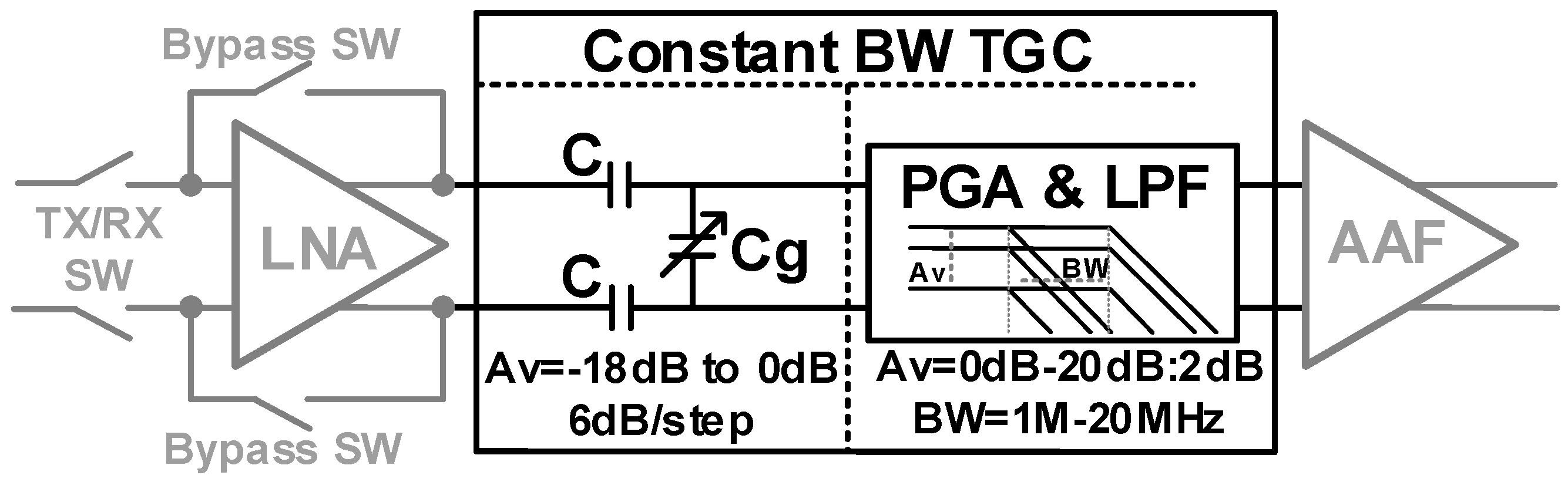
1. Introduction
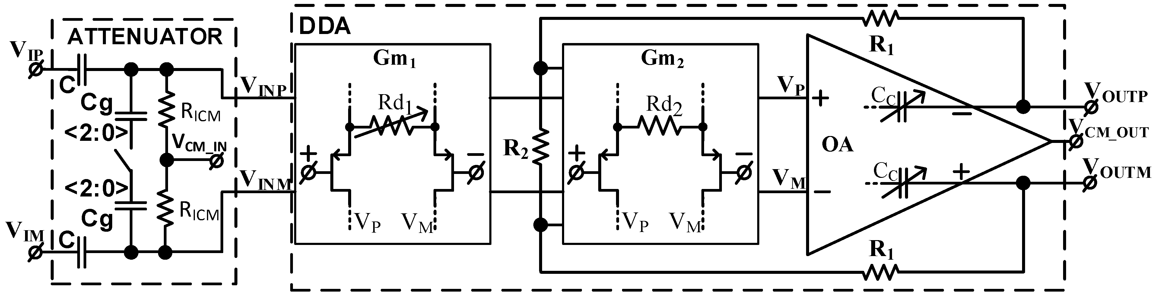
2. Circuit Implementation
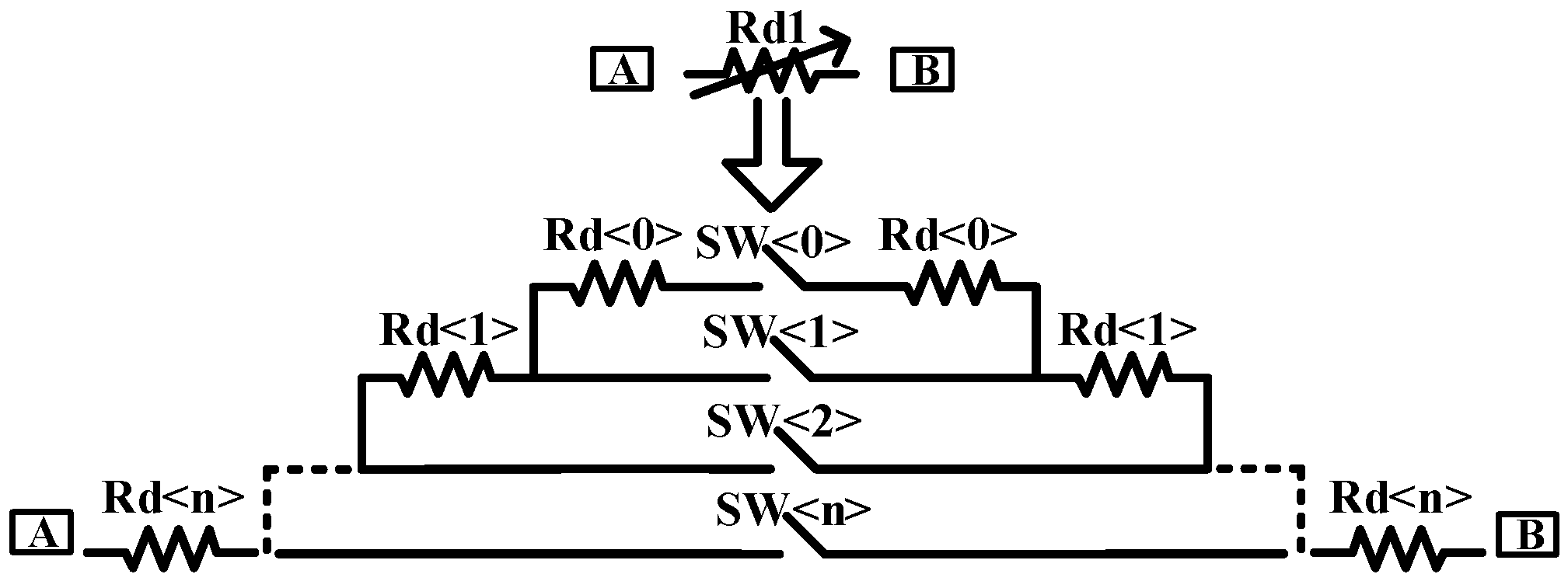
2.1. DDA-Based Programmable Bandwidth PGA Circuit
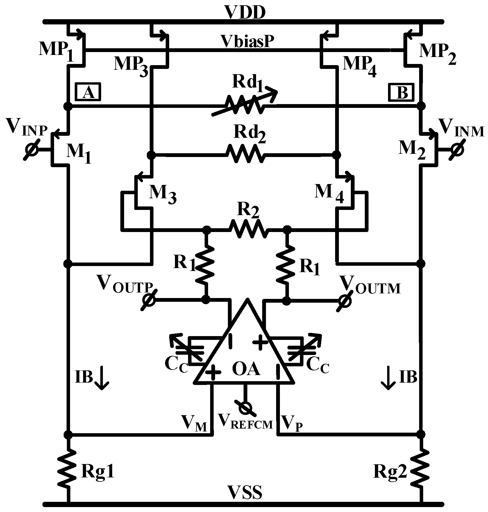
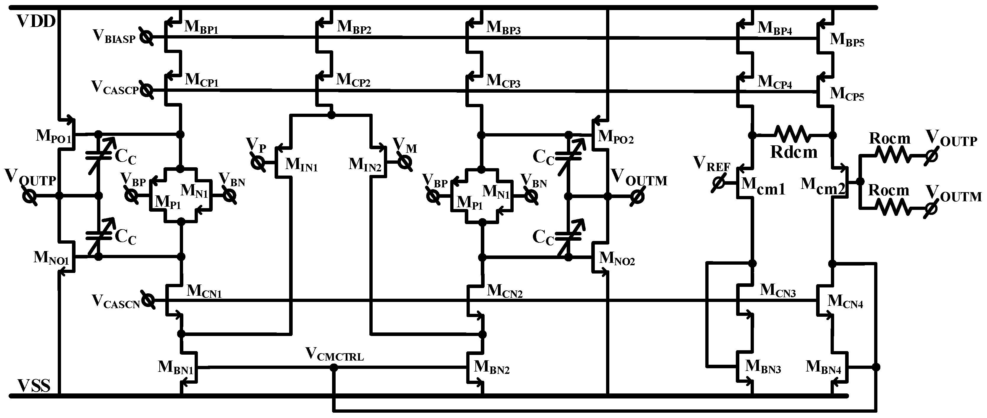
2.2. Transistor-Level Implementation of the Proposed Circuit
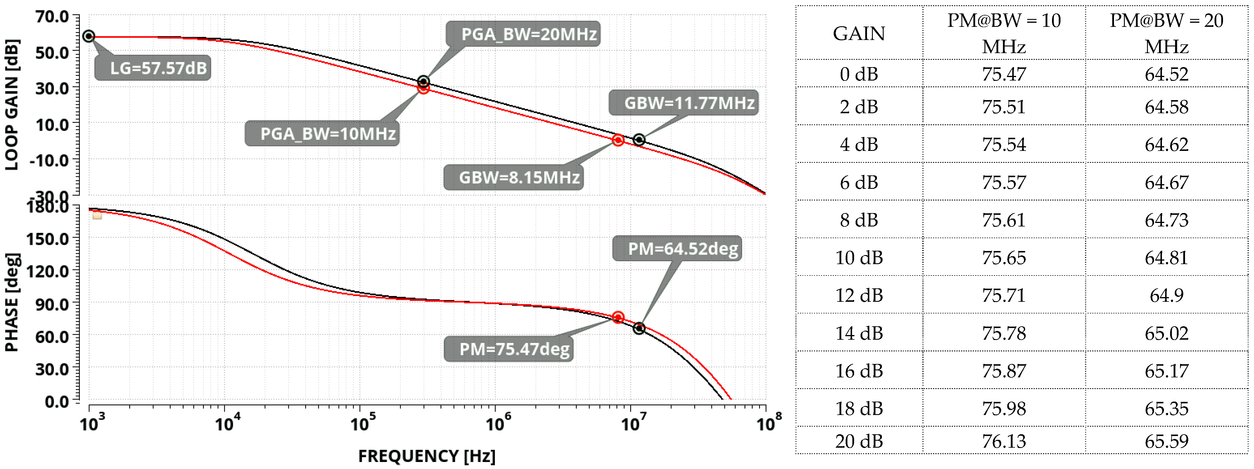
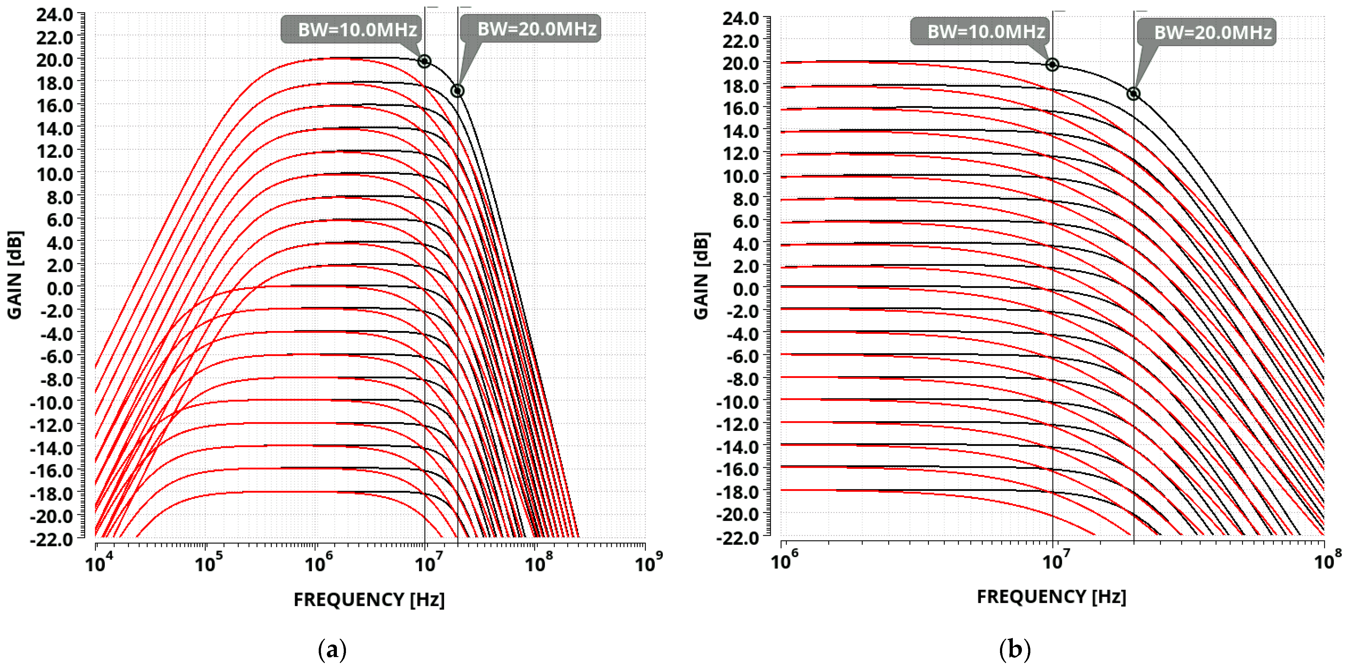
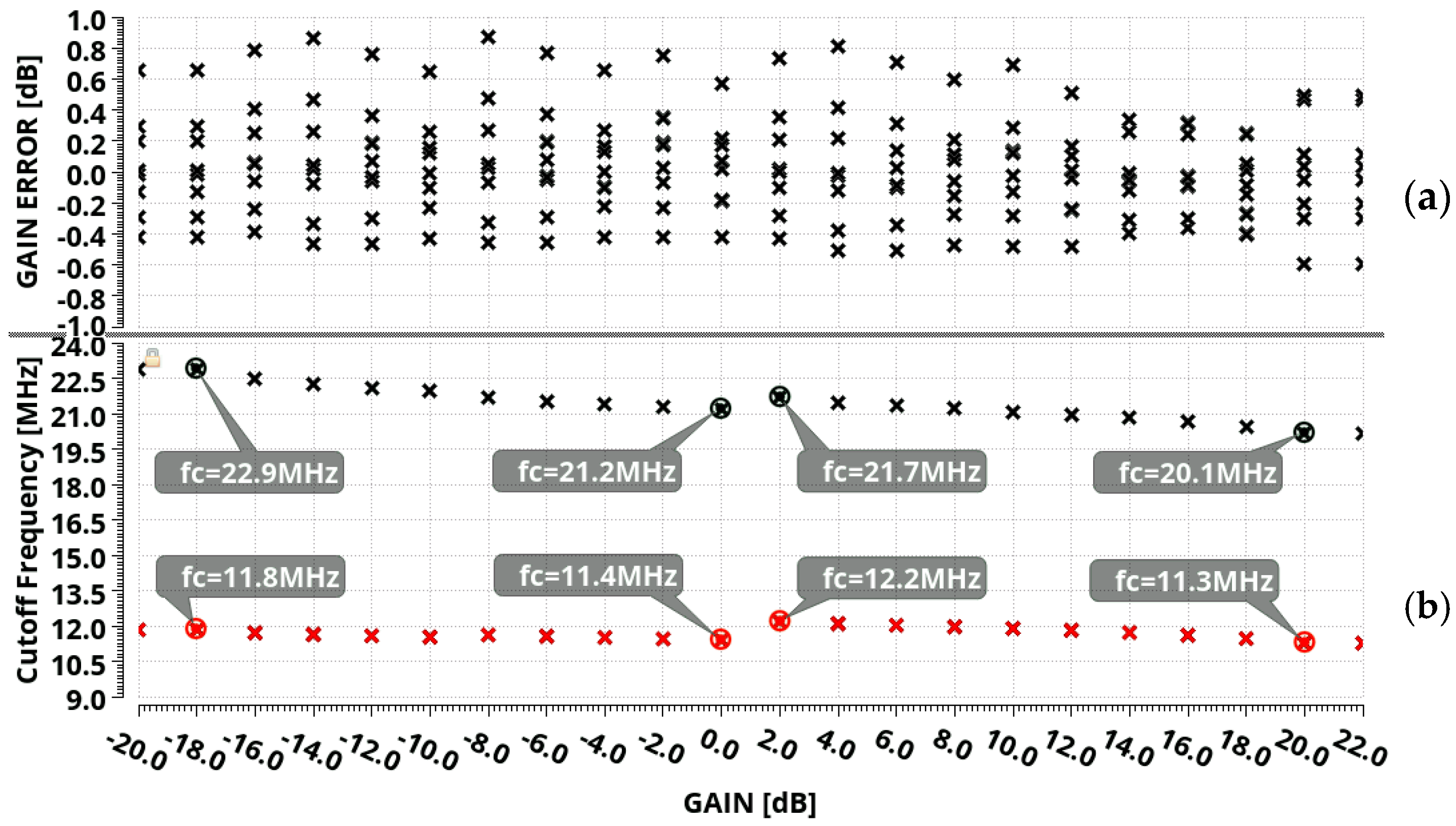
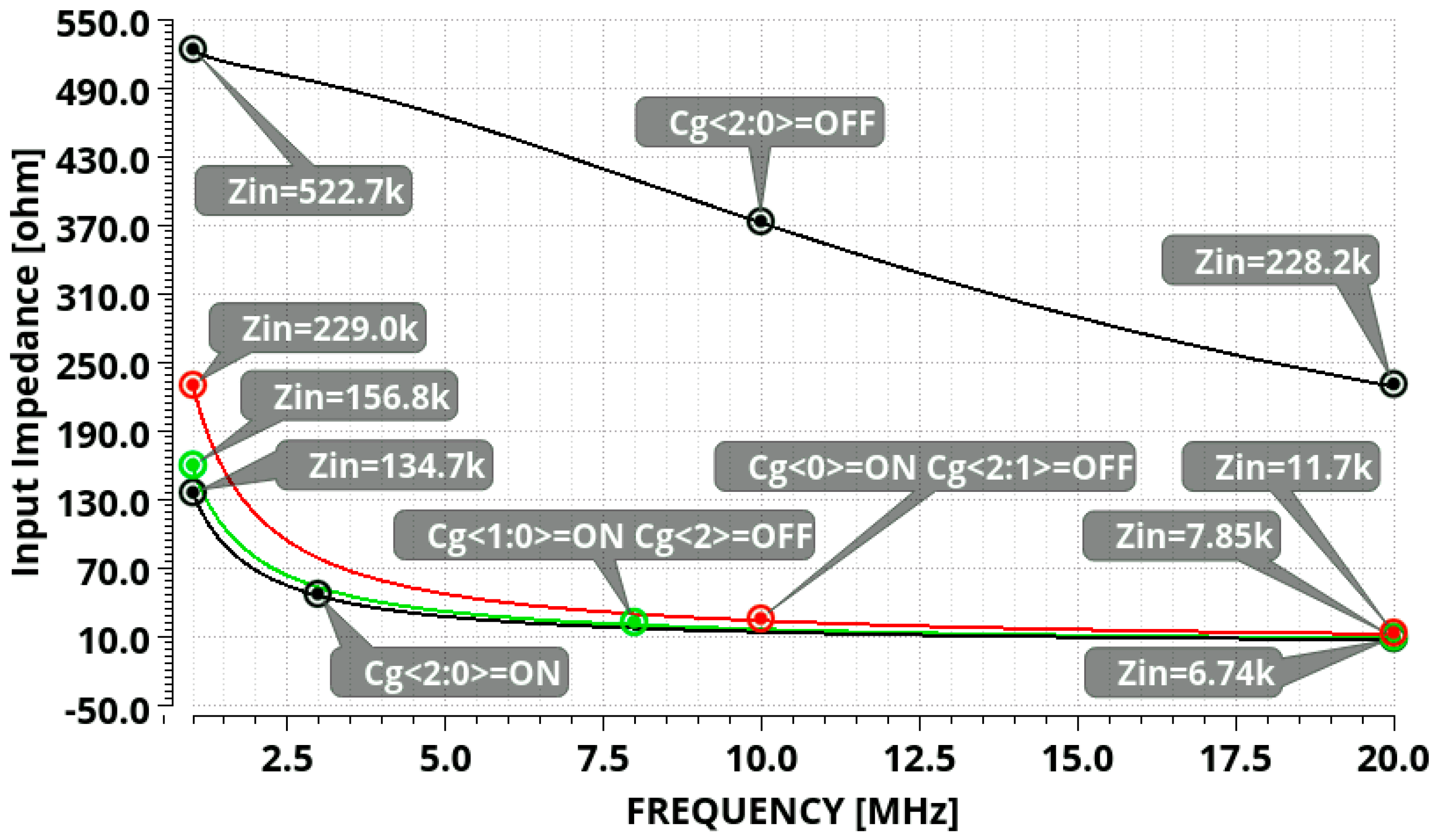
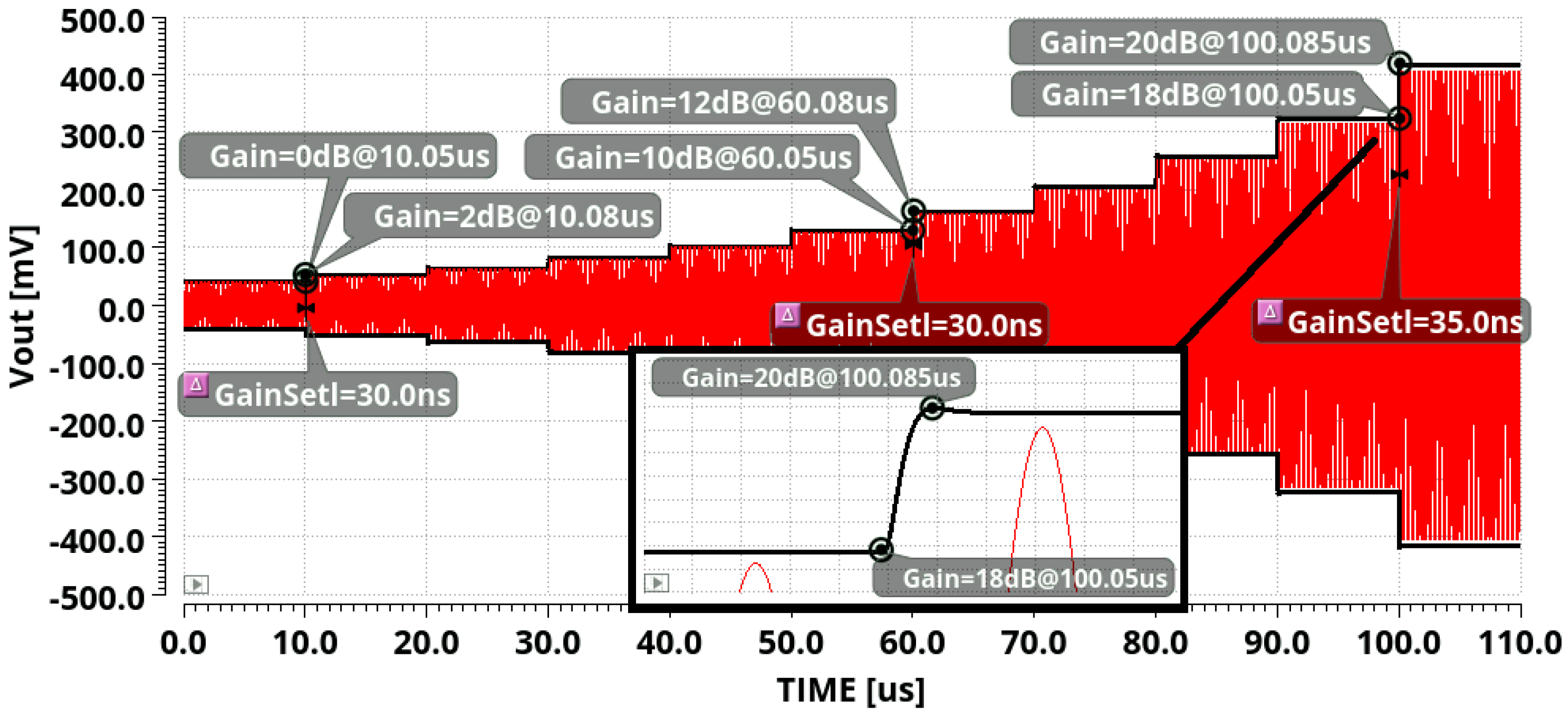
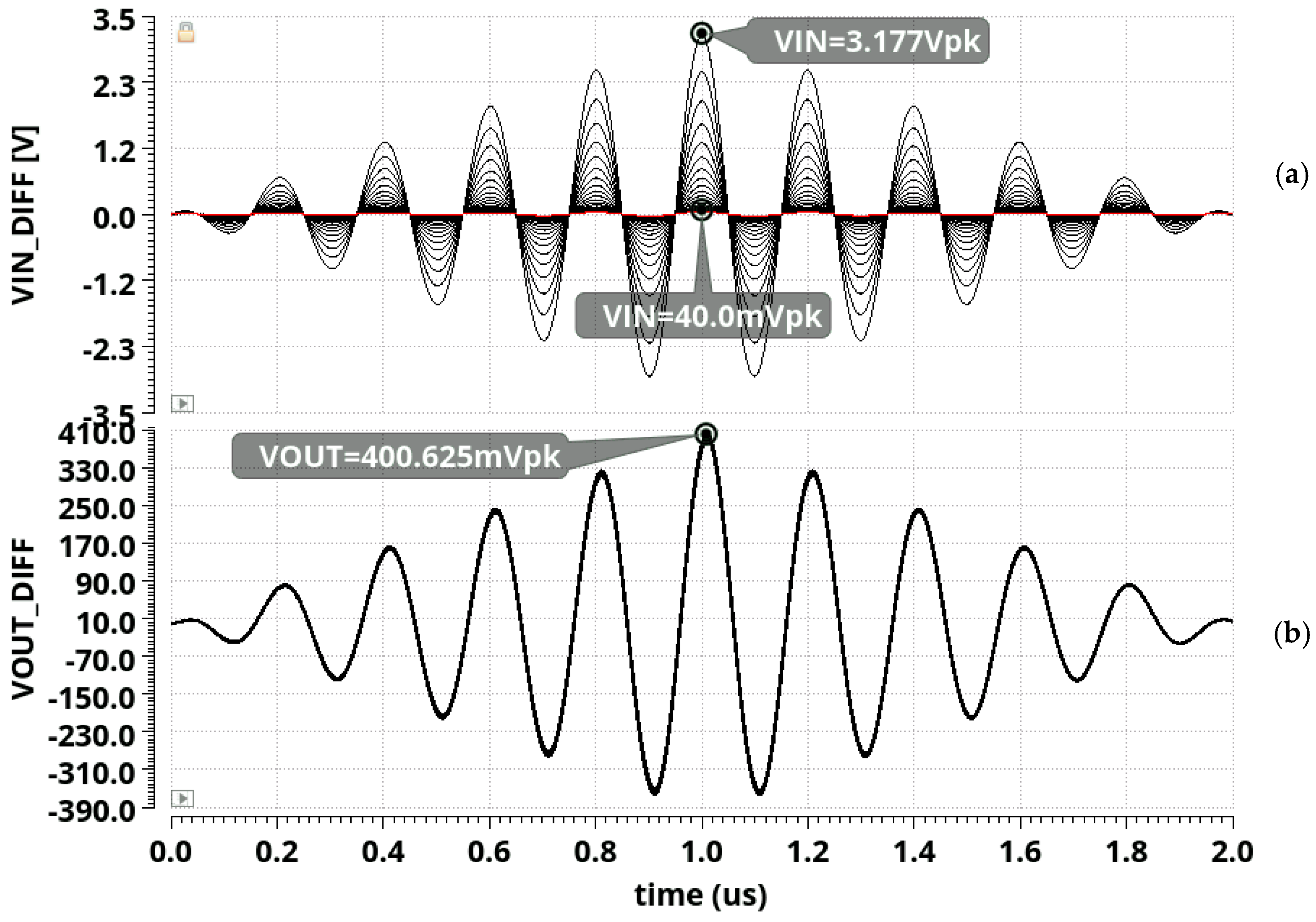
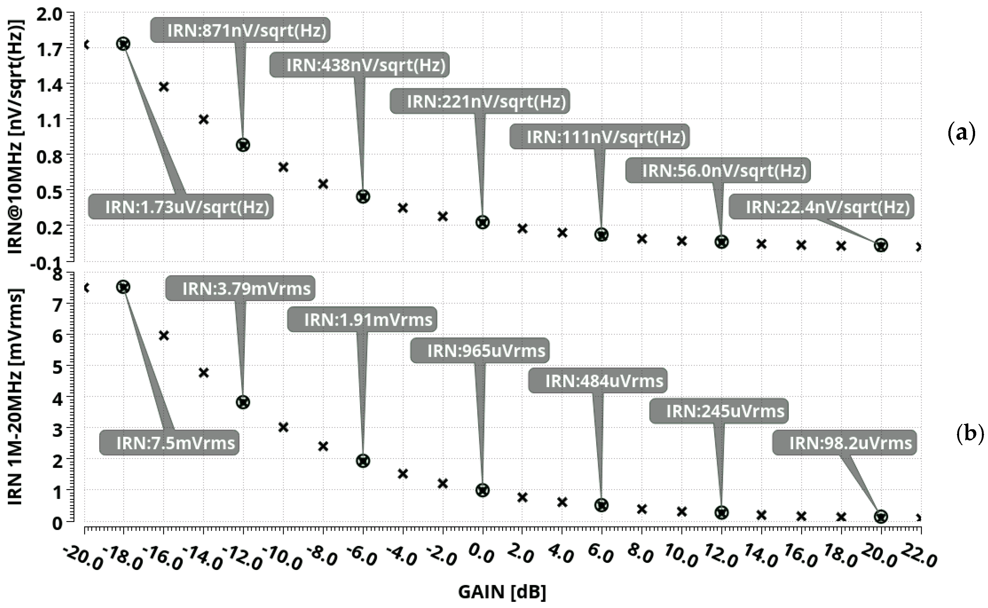
3. Simulation Results
4. Conclusions
Author Contributions
Funding
Data Availability Statement
Acknowledgments
Conflicts of Interest
References
- Moisello, E.; Novaresi, L.; Sarkar, E.; Malcovati, P.; Costa, T.L.; Bonizzoni, E. Pmut and cmut devices for biomedical applications: A review. IEEE Access 2024, 12, 18640–18657. [Google Scholar] [CrossRef]
- Yun, S.; Lee, S.; Bae, J. A 48-Channel High-Resolution Ultrasound Beamforming System for Ultrasound Endoscopy Applica-tions. Electronics 2024, 13, 568. [Google Scholar] [CrossRef]
- Zhang, Y.; Demosthenous, A. Integrated circuits for medical ultrasound applications: Imaging and beyond. IEEE Trans. Biomed. Circuits Syst. 2021, 15, 838–858. [Google Scholar] [CrossRef] [PubMed]
- Jeong, J.-Y.; Song, J.-K.; Choi, M.-S.; Hong, S.-K.; Kwon, O.-K. A high frame rate analog front-end ic with piezoelectric micromachined ultrasound transducers using analog multi-line acquisition for ultrasound imaging systems. IEEE Access 2021, 9, 119298–119309. [Google Scholar] [CrossRef]
- Choi, H. Design of Preamplifier for Ultrasound Transducers. Sensors 2024, 24, 786. [Google Scholar] [CrossRef] [PubMed]
- Jung, S.-J.; Hong, S.-K.; Kwon, O.-K. Low-Power Low-Noise Amplifier Using Attenuation-Adaptive Noise Control for Ultrasound Imaging Systems. IEEE Trans. Biomed. Circuits Syst. 2017, 11, 108–116. [Google Scholar] [CrossRef] [PubMed]
- Yu, X.; Chen, Z.; Wu, S.; Liu, L.; Chi, H.; Ye, F.; Ren, J. 28-nm cmos ultrasound afe with split attenuation for optimizing gain-range, noise, and area. IEEE Trans. Circuits Syst. I Regul. Pap. 2023, 70, 4742–4754. [Google Scholar] [CrossRef]
- Ma, L.; Wang, Z.; Xu, J.; Wang, R.; Amin, N.M. Noise analysis and optimization of programmable gain amplifier with dc offset cancelation. Circuits Syst. Signal Process. 2016, 35, 753–770. [Google Scholar] [CrossRef]
- Wu, Y.-M.; Diao, J.-G.; Luo, L.-H.; Ren, J.-Y. A dynamic range enhanced current feedback pga used in high-frequency ultrasound imaging applications. In Proceedings of the 2018 14th IEEE International Conference on Solid-State and Integrated Circuit Technology (ICSICT), Qingdao, China, 31 October–3 November 2018; IEEE: Piscataway, NJ, USA, 2018. [Google Scholar]
- Wang, Y.; Koen, M.; Ma, D. Low-noise cmos tgc amplifier with adaptive gain control for ultrasound imaging receivers. IEEE Trans. Circuits Syst. II Express Briefs 2010, 58, 26–30. [Google Scholar] [CrossRef]
- Bai, C.; Wu, J.; Chen, C.; Deng, X. A 35-dBm oip3 cmos constant bandwidth pga with extended input range and improved common-mode rejection. IEEE Trans. Circuits Syst. II Express Briefs 2016, 64, 922–926. [Google Scholar] [CrossRef]
- Sackinger, E.; Guggenbuhl, W. A versatile building block: The cmos differential difference amplifier. IEEE J. Solid-State Circuits 1987, 22, 287–294. [Google Scholar] [CrossRef]
- Park, Y.; Kim, H.; Ko, Y.; Mun, Y.; Lee, S.; Kim, J.-H.; Ko, H. Low noise cmos temperature sensor with on-chip digital calibration. Sens. Mater. 2017, 29, 1025–1030. [Google Scholar]
- Ng, K.A.; Chan, P.K. A cmos analog front-end ic for portable eeg/ecg monitoring applications. IEEE Trans. Circuits Syst. I Regul. Pap. 2005, 52, 2335–2347. [Google Scholar] [CrossRef]
- Huijsing, J.H. Instrumentation amplifiers: A comparative study on behalf of monolithic integration. IEEE Trans. Instrum. Meas. 1976, IM-25, 227–231. [Google Scholar] [CrossRef]
- Monticelli, D. A quad cmos single-supply op amp with rail-to-rail output swing. IEEE J. Solid-State Circuits 1986, 21, 1026–1034. [Google Scholar] [CrossRef]
- MSon, H.; Lee, Y.-C.; Baek, H.-M.; Choi, H.-J.; Um, J.-Y. A programmable gain amplifier with fast transient response for medical ultrasound system. In Proceedings of the 2022 19th International SoC Design Conference (ISOCC), Gangneung-si, Republic of Korea, 19–22 October 2022; pp. 302–303. [Google Scholar]
- Cho, S.-E.; Um, J.-Y.; Kim, B.; Sim, J.-Y.; Park, H.-J. A single-stage 37 db-linear digitally-controlled variable gain amplifier for ultrasound medical imaging. JSTS J. Semicond. Technol. Sci. 2014, 14, 579–587. [Google Scholar] [CrossRef]
- Koolivand, Y.; Rezaeiyan, Y.; Shoaei, O.; Jafarabadi-Ashtiani, S.; Moftakharzadeh, A.; Ahmadvand, M. Modified linear in db, sub 0.2 dB gain-step cmos programmable gain amplifier for ultrasound applications. Analog. Integr. Circuits Signal Process. 2019, 99, 497–508. [Google Scholar] [CrossRef]
- Bhattaru, P.; Krishnapura, N. A 36 dB gain range, 0.5 dB gain step variable gain amplifier with 10 to 25 MHz bandwidth third-order filter for portable ultrasound systems. In Proceedings of the 2020 33rd International Conference on VLSI Design and 2020 19th International Conference on Embedded Systems (VLSID), Bangalore, India, 4–8 January 2020; IEEE: Piscataway, NJ, USA, 2020; pp. 96–100. [Google Scholar]
- Wu, Y.; Lan, J.; Li, S.; Ye, F.; Ren, J. A ring amplifier based current feedback continuous time pga for high frequency ultrasound applications. In Proceedings of the 2019 IEEE 62nd International Midwest Symposium on Circuits and Systems (MWSCAS), Dallas, TX, USA, 4–7 August 2019; pp. 141–144. [Google Scholar]


| ATTENUATOR from Figure 2 | Class-AB FD-OA from Figure 4 | |||
|---|---|---|---|---|
| RICM (kΩ) | 250 | MIN1,2 (N × W/L) | 2 × 20 µ/200 n | Mirror ratios: DIODE M = 1 with bias current 5 µ A |
| C/CG<2:0 > (pF) | 2.7/7 × 2.7 | MPO1,2 (W/L) | 10 µ/200 n | |
| TSW (M × (W/L)) | 2 × (4 µ/180 n) | MNO1,2 (N × W/L) | 6 × 5 µ/200 n | MBP1, MBC1: M = 4 |
| PGA CORE from Figure 3 | MBPX (W/L) | 10 µ/200 n | MBP2, MBC2: M = 2 | |
| M1,2,3,4 (M × (N × W/L)) | 2 × (2 × 20 µ/200 n) | MCPX (W/L) | 10 µ/180 n | MBP1,2cm, MBC1,2cm: M = 2 |
| MP1,2,3,4 (M × (N × W/L)) | 10 × (1 × 12 µ/800 n) | MBNX (W/L) | 5 µ/5 µ | MBN1,2: M = 3 |
| Rd1 total/Rd2 (kΩ) | 32.2/2 × 7.5 | MCNX (W/L) | 5 µ/180 n | McN1,2: M = 8 |
| R1/R2 (kΩ) | 30/60 | MN (W/L) | 5 µ/500 n | MB1,2cm, MC1,2cm: M = 1 |
| Rg1,2 (kΩ) | 4 | MP (W/L) | 10 µ/500 n | MN,P: M = 2 |
| CC total (pF) | 1.2 | Mcm1,2 (W/L) | 4 µ/300 n | |
| IB (µ A) | 100 | Rdcm, Rocm (kΩ) | 100 | |
| Parameter/Units | This Work | [9] | [11] | [17] | [18] | [19] | [20] | [21] |
|---|---|---|---|---|---|---|---|---|
| Gain range (dB) | −18 to 20 | 0 to 24 | 0 to 14 | 0 to 30 | −10 to 27 | −24 to 24 | −12 to 24 | 10 to 40 |
| Gain step (dB) | 2 | 4 | 2 | 3.75 | 2 | 0.19 | 0.5 | 5 |
| Gain error (dB) | 0.9 | - | - | - | 3.9 | - | - | - |
| Cutoff Frequency, fC (MHz) | 20 | 20 | 30 | 9.4 | 0.02–8 | 82 | 10–25 | 40 |
| VoutMAX 1 (VppDiff) | 0.8 | 0.7 | 1 | 0.15 | 0.94 | 2 | 2 | 0.8 |
| ) | 22.4 at 10 MHz | - | 56 | 4.8 | - | 4.1 | 4.25 | 13.7 |
| IRN RMS (µV) | 98.1 | - | 244.1 | - | - | - | 18.5 | - |
| Supply Voltage (V) | 1.8 | 1.05 | 1.8 | 1.8 | 3.3 | 1.8 | 1.8 | 1.8 |
| Supply Current (mA) | 0.6 | 4.76 | 0.58 | 0.61 | 0.58 | 4.8 | 2 | 2.33 |
| Power (mW) | 1.08 | 5 | 1.04 | 1.1 | 1.9 | 8.64 | 3.6 | 4.2 |
| Process (µm) | 0.18 | 0.028 | 0.18 | 0.18 | 0.35 | 0.18 | 0.18 | 0.18 |
| FOM | 1176.78 | 28.01 | 114.4 | 26.37 | 220.94 | 4664.77 | 827.31 | 135.68 |
Disclaimer/Publisher’s Note: The statements, opinions and data contained in all publications are solely those of the individual author(s) and contributor(s) and not of MDPI and/or the editor(s). MDPI and/or the editor(s) disclaim responsibility for any injury to people or property resulting from any ideas, methods, instructions or products referred to in the content. |
© 2025 by the authors. Licensee MDPI, Basel, Switzerland. This article is an open access article distributed under the terms and conditions of the Creative Commons Attribution (CC BY) license (https://creativecommons.org/licenses/by/4.0/).
Share and Cite
Kovács, I.; Coste, P.; Neag, M. Programmable Gain Amplifier with Programmable Bandwidth for Ultrasound Imaging Application. Electronics 2025, 14, 1186. https://doi.org/10.3390/electronics14061186
Kovács I, Coste P, Neag M. Programmable Gain Amplifier with Programmable Bandwidth for Ultrasound Imaging Application. Electronics. 2025; 14(6):1186. https://doi.org/10.3390/electronics14061186
Chicago/Turabian StyleKovács, István, Paul Coste, and Marius Neag. 2025. "Programmable Gain Amplifier with Programmable Bandwidth for Ultrasound Imaging Application" Electronics 14, no. 6: 1186. https://doi.org/10.3390/electronics14061186
APA StyleKovács, I., Coste, P., & Neag, M. (2025). Programmable Gain Amplifier with Programmable Bandwidth for Ultrasound Imaging Application. Electronics, 14(6), 1186. https://doi.org/10.3390/electronics14061186