Abstract
The timing jitter of a single-photon avalanche diode (SPAD) plays a critical role in the design and optimization of front-end circuits. This paper proposes a simplified timing jitter model based on Verilog-A. This model uses random numbers to determine the locations of photon absorptions and carrier avalanches based on absorption and avalanche probabilities, thereby achieving a calculation of the response time. By introducing photon detection probability, the model has corrected the response time obtained under ideal assumptions and achieved compatibility with excess bias voltage effects, which can describe the Gaussian peak of the timing jitter concisely and effectively. The simulation results are in good agreement with the measurement results, demonstrating the advantages of this model in terms of accuracy, flexibility, and adaptability. The model provides support for the collaborative optimization of the design of SPAD devices and circuits.
1. Introduction
The single-photon avalanche diode (SPAD), also known as the Geiger-mode avalanche photo diode (Geiger-mode APD), has been a significant driver of advancements in fields such as LiDAR, quantum communication, biological fluorescence detection, autonomous driving, etc. [1,2,3], due to its excellent detection sensitivity, outstanding timing resolution, low cost, and high reliability [4,5,6].
Timing jitter refers to the uncertainty in the response time seen during the photon detection process in a SPAD, and it is typically quantified by the full width at half maximum (FWHM) of the timing histogram [5]. Timing jitter is one of the key parameters that affect the phase margin and timing constraints of SPAD circuit designs, especially in high-precision time measurement and high-speed signal processing applications. In order to accurately evaluate the impact of timing jitter on circuit performance and provide a basis for circuit design and performance optimization, there is an urgent need to develop an effective SPAD timing jitter model which must be compatible with mainstream commercial circuit simulation tools such as Cadence Spectre and Synopsys HSPICE [5,6,7].
The avalanche multiplication process in SPAD exhibits a high degree of randomness, which significantly increases the complexity of developing an accurate timing jitter model. Currently, advanced predictions of timing jitters primarily rely on Monte Carlo simulations. Shiyu Xie et al. [8] developed a 3D Simple Monte Carlo Statistical Model that includes an ionization coefficient and avalanche gain calculations, takes into account the influence of the doping concentration, and is capable of predicting a device’s timing jitter. Rémi Helleboid et al. [9] proposed an electron transport and avalanche simulation method based on the Fokker–Planck viewpoint on the advection diffusion equation, which achieves the simultaneous calculation of carrier transport and collisional ionization, greatly reducing computational consumption and achieving extremely high accuracy. Yang Liu et al. [10] proposed a model that combines one-dimensional avalanche accumulation and two-dimensional avalanche diffusion, which reduces the consumption of computational resources by simulating the avalanche propagation process in segments. However, these methods based on Monte Carlo require the simulation and statistical analysis of a large number of charge carriers. Their high computational and time costs limit their application in large-scale SPADs and circuit design [8,9,10,11].
In previous studies, many researchers have modeled timing jitter based on statistical regularities. Feiyang Sun et al. [12], from another perspective, used analytical statistical methods to solve the two-dimensional avalanche current equation to model a Gaussian peak timing jitter. Rémi Helleboid et al. [13] developed a high-precision simulation by modeling the carrier’s trajectory, avalanche breakdown probability, and charge transport using a one-dimensional model of the electric field lines, which also ensures compatibility with Technology Computer Aided Design (TCAD) software. Kaveh Eyvazi et al. [14] proposed an analytical model of timing jitter for characterizing the avalanche multiplication rate of SPADs based on Fourier series, which demonstrates superior accuracy compared to traditional numerical models. However, despite these models making significant analytical and numerical advancements, they generally require solving complex differential equations and lack compatibility with commercial circuit simulators. Therefore, developing a timing jitter model that maintains accuracy, reduces computational burden, and is compatible with commercial circuit simulators has become a focal point of current research [5,6,12,13,14].
In this paper, we propose a simplified SPAD timing jitter model in Verilog-A HDL based on the SPAD avalanche principle and previous SPAD models, which can seamlessly adapt to mainstream commercial circuit simulators. To achieve efficient SPAD response time estimations, this paper constructs a simplified one-dimensional absorption–multiplication model by utilizing the distribution of absorption and avalanche probabilities and employing random numbers to determine key photon absorption and avalanche locations. This approach circumvents the need for the extensive simulation of carriers, as in Monte Carlo methods, and the complex calculations used for solving differential equations in numerical models. Furthermore, the influence of the excess bias voltage is incorporated into the model to ensure its accuracy under different working conditions. The model shows good agreement with experimental data and provides powerful support for the collaborative optimization of SPAD devices and circuits.
2. Simplified Timing Jitter Model
2.1. The Structure and Principle of SPAD
A SPAD is essentially a special p-n junction that operates using an avalanche multiplication mechanism. When the bias voltage is higher than the reverse breakdown voltage, the SPAD works in Geiger mode; otherwise, it works in linear mode. Although a SPAD can achieve significant gain through the avalanche multiplication process when in Geiger mode, there are huge safety risks. When an avalanche event happens in a SPAD, the process will persist, without external intervention, until the device is destroyed. Therefore, once the SPAD enters avalanche, it is necessary to actively lower the voltage across the SPAD using circuits to force it into linear mode, making the electric field strength insufficient to sustain the carrier’s avalanche ionization process [5,6].
In order to further improve detection efficiency, mainstream designs usually optimize device performance by separating the absorption and avalanche processes. By optimizing the depletion region, a structure with a high-electric-field multiplication region and a low-electric-field absorption region as its core is formed [5,12,15], as shown in Figure 1.
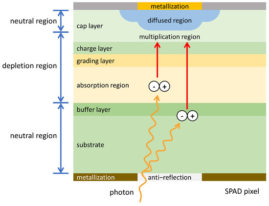
Figure 1.
Structure of absorption, grading, charge, and multiplication (SAGCM) SPAD.
After the photons are absorbed in the absorption region, they are converted into electron–hole pairs. These carriers are subsequently injected into the multiplication region under the influence of the built-in electric field. Within the multiplication region, the carriers are accelerated by the strong electric field, causing them to undergo frequent collisions with the lattice, leading to avalanche multiplication. The carriers then exit the multiplication region and enter the neutral region, and are eventually collected by the electrodes.
During this process, when the carriers that trigger the avalanche event originate from the depletion region, the response time is relatively short, and it follows a typical Gaussian distribution [16,17]. However, when the avalanche event is triggered by carriers diffusing from the neutral region into the depletion region, there is a longer time delay and an exponential tail characteristic appears [16,17], as shown in Figure 2.
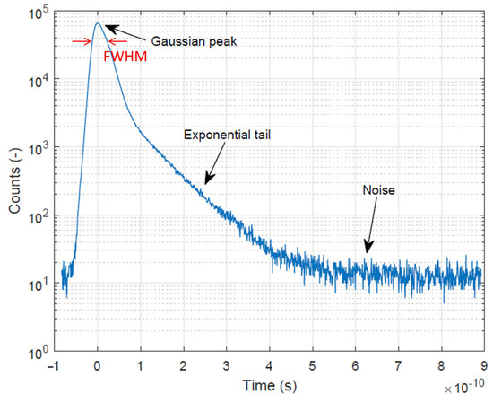
Figure 2.
Typical SPAD timing histogram.
2.2. Modeling of Response Time
Since the carriers’ lifetime is much longer than the response time [18], the effects of carrier recombination are neglected. Furthermore, to make the model simple enough to run on circuit simulations and avoid the need for precise calculations of a large number of carriers, the following assumptions are made:
- Only the absorption region is capable of absorbing photons.
- The quantum efficiency of the absorption region is assumed to be 100%, meaning that each photon generates one electron–hole pair.
- Only the multiplication region can perform avalanche multiplication, and the probability of avalanche events occurring is 100%.
- The avalanche multiplication process is assumed to occur instantaneously within an extremely short period of time.
Based on the aforementioned assumptions, the avalanche multiplication process of a SPAD can be simplified into three stages:
- Carriers are generated at a location in the absorption region and are injected into the multiplication region.
- Within the multiplication region, carriers are accelerated by the strong electric field, gradually gathering momentum until they trigger the first avalanche ionization at a location.
- Carriers continuously perform avalanche multiplication, generating a sufficiently large current and exiting the multiplication region under the influence of the built-in electric field.
Therefore, the response time is defined as
where refers to the absorption region transit time, representing the time required for carriers to migrate from their generation point in the absorption region to the multiplication region; refers to the momentum accumulation time, indicating the period during which carriers accumulate momentum in the multiplication region prior to the avalanche process; and refers to the multiplication region transit time, which indicates the time required for the large number of carriers produced by the avalanche to move from the multiplication region to the neutral region.
2.2.1. Absorption Region Transit Time
The semiconductor’s ability to absorb photons exhibits exponential decay, meaning that the location at which carriers are generated follows an exponential distribution [19,20]; that is
where is the location where carriers are generated in the absorption region and is the absorption coefficient of the semiconductor.
So, the absorption region transit time is as follows:
where is the thickness of the absorption region and is the drift velocity of the carriers.
2.2.2. Momentum Accumulation Time
In the multiplication region, carriers require a period of time to accumulate sufficient momentum, even if they are generated at the location of the maximum electric field in the depletion region. However, calculating the momentum accumulation time accurately and conveniently is challenging. Fortunately, when the bias voltage exceeds 19 V, the statistical fluctuation of the momentum accumulation time stabilizes to an almost constant value, which is typically less than 10 ps [17].
For most SPADs, the timing jitter is on the order of tens to hundreds of picoseconds. The value of is nearly two orders of magnitude smaller than the value of . Thus, the impact of the momentum accumulation time on the timing jitter can essentially be neglected.
2.2.3. Multiplication Region Transit Time
The probability of a carrier avalanche varies at different locations within the multiplication region. A random number conforming to the probability density is generated based on the avalanche probability distribution and considered as the avalanche location .
According to our fourth assumption, the multiplied carriers are considered to be located at approximately the same location as the carriers that initiated the avalanche. Thus, the multiplication region transit time is given by
where is the thickness of the multiplication region.
2.2.4. Response Time Correction
The previous assumptions were absolutely ideal. In reality, not every photon is absorbed by the semiconductor and generates carriers, and not every carrier entering the multiplication region can trigger an avalanche event. Additionally, the time required for the avalanche to generate a sufficient number of carriers is not instantaneous. All these unideal factors make the photon detection probability (PDP), which is defined as the ratio of the number of SPAD avalanche events to the number of incident photons, less than 100%. Therefore, the PDP is used to correct the response time, and it can be calculated as follows [21,22]:
where is quantum efficiency and is the avalanche probability, which is the integral of the avalanche probability distribution in the multiplication region.
The absorption region transit time and the multiplication region transit time are, respectively, corrected to
So, the response time is thus adjusted to
and the total timing jitter of the SPAD is
It is indeed challenging to precisely determine the quantum efficiency and avalanche probability of the SPAD. To facilitate calculations, this model makes conservative estimates; that is
In different working environments, the PDP of a SPAD varies. According to some previous research results [12,15,16,23], the PDP generally exhibits an exponential growth relationship with the excess bias voltage , which is the difference between the bias voltage and breakdown voltage.
Based on Equation (10), it is evident that the response time or timing jitter exhibits an exponential decay relationship with the excess bias voltage in our simplified model. This trend is consistent with previous findings [10,11,20]. Our simplified model naturally incorporates the impact of different working environments on the timing jitter, which can reflect the dynamic performance variations seen in the SPAD under different conditions.
3. Verilog-A HDL Implementation
3.1. Jitter Module
The first step of the simplified time jitter model is to obtain the photon absorption location and the location of the first avalanche collision. The location where photons are absorbed and carriers are generated satisfies an exponential distribution with a mean of , so the system function of Verilog-A HDL is used to generate a random number:
Verilog-A exhibits limited computational capabilities in handling calculus, making the direct calculation of Equation (3) particularly challenging. However, in most cases, the spatial variation of the electric field in the absorption region is relatively smooth, and the field strength is low. When high precision is not required, the electric field can be approximated as a constant. Therefore, Equation (3) can be simplified as follows:
The location of the carrier avalanche is related to the distribution of the avalanche triggering probability in the multiplication region. Using TCAD software, the distribution of the avalanche probability and the drift velocity can be obtained. According to our third assumption, the is scaled. Thus,
When high precision is not required, it can be approximated, based on experience, as follows [12,13,24]:
where k is an empirical parameter that, to some extent, allows the avalanche probability distribution to take into account the increase in electric field strength from the absorption region to the multiplication region, as well as the distance traveled by carriers in the multiplication region due to their accumulated momentum, and, in most cases, k ≈ 0.1∼0.4 [12,13,19].
We can generate an avalanche location that conforms to the scaled avalanche probability by using the Verilog-A system function combined with the acceptance–rejection method [25,26]. Based on the drift velocity , we can calculate the integral result of Equation (5) in advance and use the lookup table method in Verilog-A to obtain the multiplication region transit time.
The final step is to correct the response time using the excess bias voltage and photon detection probability, PDP, in accordance with Equation (7).
3.2. SPAD Circuit Simulation Model
Based on the structure of a traditional SPAD circuit simulation model, a jitter module, which is used for calculating response times, has been added. The state transition diagram of the complete SPAD circuit simulation model is shown in Figure 3. The SPAD circuit simulation model consists of a DC/AC module, a trigger module, a jitter module, a dark count rate (DCR) module, and an after-pulse (AP) module. Similar to the actual SPAD, the SPAD circuit simulation model also has two modes: Geiger and linear. When in Geiger mode, the model can be quenched and enter linear mode. In linear mode, the model can re-enter Geiger mode when the bias voltage is higher than the breakdown voltage.
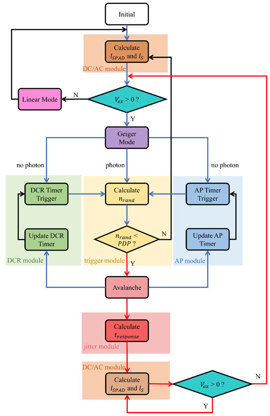
Figure 3.
The state transition diagram of the SPAD circuit simulation model.
Firstly, the internal parameters and signals of the model are initialized, and the DC/AC module calculates the avalanche current or breakdown current and the reverse saturation current or dark current . Then, we can determine whether the working mode of the SPAD is its linear mode or Geiger mode based on the excess bias voltage .
When the SPAD runs in linear mode, the DC/AC module calculates and and outputs . The trigger module, DCR module, jitter module, and AP module do not run in linear mode.
When the SPAD runs in Geiger mode, the trigger module will use to calculate a random number that follows a uniform distribution of 0–1 when it receives a signal from a photon, DCR module, or AP module. If is smaller than the PDP, the model enters an avalanche state, and it updates the timers of the DCR module and AP module. Then, the jitter module calculates . Subsequently, the DC/AC module calculates and and outputs after a delay of . Finally, the model determines the working state based on : if , the model maintains a self-sustaining avalanche state, returns to the DC/AC module, and outputs ; if , the model is quenched. The working process of the DCR module and AP module is detailed in [6].
4. Simulation and Verification
4.1. Measurement Platform and Simulation Parameters
As shown in Figure 4 and Figure 5, a light pulse was generated by a picosecond pulse laser (PDL800D from PicoQuant in Berlin, Germany) with a typical pulse width of 20 ps; the timing jitter was recorded using a time-correlated single-photon counting system (FT1010 from Siminics in Shanghai, China); the time delay and gate signal were controlled by a digital delay/pulse generator (DG645 from Stanford Research Systems (SRS) in Sunnyvale, CA, USA); and a detachable black aluminum box was used to shield the external light environment during measurement.
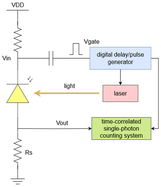
Figure 4.
A principle block diagram of the measurement platform.
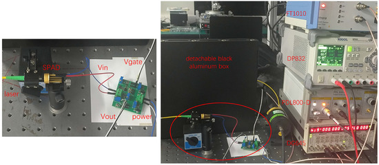
Figure 5.
Measurement platform and equipment used.
The detector uses an InGaAs/InP SPAD (from Xi’an Institute of Optics and Precision Mechanics, Chinese Academy of Sciences in Xi’an, China) designed by our research group, as shown in Figure 6a. Its built-in electric field distribution was obtained through TCAD simulation during its design, as shown in Figure 6b,c. The circuit simulation platform uses Cadence Virtuoso (version: ic6.1.7-64b. 5002) and the simulator used is Spectre. The device specs of the InGaAs/InP SPAD and the parameters used in this simulation are shown in Table 1.
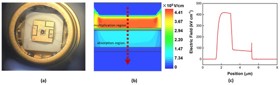
Figure 6.
The InGaAs/InP SPAD used: (a) appearance; (b) built-in electric field distribution; (c) relationship between built-in electric field and position.

Table 1.
The device specs of the InGaAs/InP SPAD and the parameteres of the timing jitter model.
4.2. Results and Discussion
The response timing histograms from measurements and simulations at different excess bias voltages are shown in Figure 7, indicating that the proposed simplified SPAD time jitter model can effectively restore the Gaussian distribution curve of the time jitter and accurately estimate the FWHM. The relative error between the measurement and simulation is below 15%, as shown by the green in Figure 8. However, near the Gaussian peak, the simulation results of the response time are slightly earlier than the measurement results and there is slight distortion in the shape. This is due to our neglect of during modeling and our fourth assumption, which states that avalanches occur instantaneously. There is also a deviation in the model at the end of the time jitter curve. This deviation is mainly due to the model not considering the formation mechanism of exponential tails.
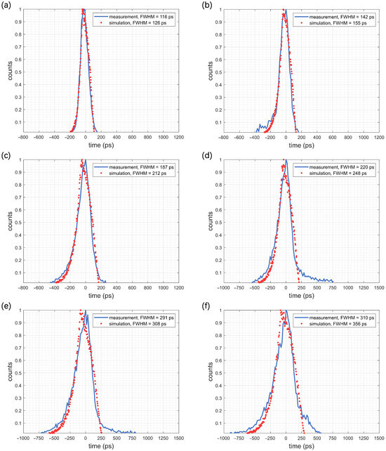
Figure 7.
The response timing histograms of the SPAD, at a temperature of 297 K with a 1550 nm wavelength beam at a frequency of 20 kHz. The excess bias voltage in each histogram is (a) 5 V; (b) 4 V; (c) 3 V; (d) 2 V; (e) 1 V; and (f) 0.5 V.
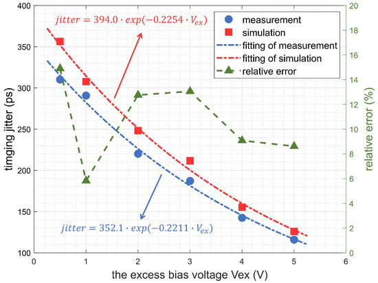
Figure 8.
The timing jitter of the SPAD vs. the excess bias voltage at a temperature of 297 K and with a 1550 nm wavelength beam with a frequency of 20 kHz.
As seen in Figure 8, both the measurement and simulation results exhibit a characteristic exponential decay of the time jitter with the increase in the excess bias voltage, which is consistent with previous findings [10,15,17,24]. The fitting for the timing jitter measurement is , while the fitting of the simulation is , which can be used for a quick estimation of the timing jitter.
The simulation results are consistently slightly larger than the measured values, primarily due to conservative adjustments made to the and . Additionally, the model omits , which constrains the deviation of the simulation results in a fortunate manner, preventing the excessive divergence from the actual measurements that could be caused by these conservative adjustments to a certain degree.
Table 2 shows a summary of the comparison of our model with state-of-the-art SPAD jitter models. We comprehensively evaluated the models in terms of four aspects: method, error, computational consumption, and whether it is compatible with circuit simulators. It can be seen that our model performs well in precision and shows significant advantages in computational efficiency and compatibility.
Table 2.
Summary of comparison of our model with state-of-the-art jitter models.
5. Conclusions
In this paper, a simplified SPAD timing jitter model in Verilog-A that can be readily implemented in circuit simulators was developed. Compared to the Monte Carlo method and numerical models, this model offers significant speed advantages. The simulation results align well with actual measurements. This simplified model meets the precision requirements for a SPAD timing jitter in circuit design processes, making it highly suitable for the simulation and optimization of SPAD front-end circuits, with excellent versatility and compatibility.
Author Contributions
Conceptualization, L.X. and X.W.; methodology, L.X. and L.L.; software, L.X.; validation, Y.C., K.Q. and Z.X.; formal analysis, L.X. and L.L.; investigation, L.X., Y.C. and K.Q.; resources, Y.C. and K.Q.; data curation, Z.X.; writing—original draft preparation, L.X., L.L. and Z.X.; visualization, J.W., C.S. and T.L.; project administration, F.Y. and X.W.; funding acquisition, X.W. All authors have read and agreed to the published version of the manuscript.
Funding
This research was funded by the National Natural Science Foundation of China (NO. 62075236), the Key Research and Development Program of Shaanxi (NO. 2024GX-YBXM-090), the Youth Innovation Promotion Association of Chinese Academy of Sciences (NO. 2020397), the Rising Research Star of Shaanxi Province (NO. 2021SR5061), and the Shenzhen Major Science and Technology Project (NO. KJZD20231023100501003).
Data Availability Statement
The data from the study can be made available by the corresponding author (X.W.: wangxing@opt.ac.cn) upon reasonable request.
Conflicts of Interest
The authors declare no conflicts of interest.
Abbreviations
The following abbreviations are used in this manuscript:
| SPAD | Single-photon avalanche diode |
| APD | Avalanche photo diode |
| DCR | Dark count rate |
| AP | After-pulse |
| FWHM | Full width at half maximum |
| PDP | Photon detection probability |
References
- Kumagai, O.; Ohmachi, J.; Matsumura, M.; Yagi, S.; Tayu, K.; Amagawa, K.; Matsukawa, T.; Ozawa, O.; Hirono, D.; Shinozuka, Y.; et al. 7.3 A 189 × 600 back-illuminated stacked SPAD direct time-of-flight depth sensor for automotive LiDAR systems. In Proceedings of the 2021 IEEE International Solid-State Circuits Conference (ISSCC), San Francisco, CA, USA, 13–22 February 2021; Volume 64, pp. 110–112. [Google Scholar]
- Dalla Mora, A.; Tosi, A.; Tisa, S.; Zappa, F. Single-photon avalanche diode model for circuit simulations. IEEE Photonics Technol. Lett. 2007, 19, 1922–1924. [Google Scholar] [CrossRef]
- Tang, Y.; Wang, R.; Yang, X.; He, T.; Liu, Y.; Zhao, M. High crosstalk suppression in InGaAs/InP single-photon avalanche diode arrays by carrier extraction structure. Nat. Commun. 2024, 15, 593. [Google Scholar] [CrossRef]
- Qiao, K.; Chang, Y.; Xu, Z.; Yin, F.; Liu, L.; Wang, J.; Su, C.; Xu, L.; Fang, M.; Liu, C.; et al. Analysis of InGaAs/InP Single Photon Avalanche Diodes with Multiplication Width in Sub-Micron. IEEE J. Quantum Electron. 2024, 60, 1–7. [Google Scholar] [CrossRef]
- Qian, X.; Jiang, W.; Elsharabasy, A.; Deen, M.J. Modeling for single-photon avalanche diodes: State-of-the-art and research challenges. Sensors 2023, 23, 3412. [Google Scholar] [CrossRef] [PubMed]
- Xie, S.; Liu, J.; Zhang, F. An accurate circuit model for the statistical behavior of InP/InGaAs SPAD. Electronics 2020, 9, 2059. [Google Scholar] [CrossRef]
- Helleboid, R.; Rideau, D.; Grebot, J.; Nicholson, I.; Moussy, N.; Saxod, O.; Saint-Martin, J.; Pala, M.; Dollfus, P. Modeling of SPAD avalanche breakdown probability and jitter tail with field lines. Solid-State Electron. 2022, 194, 108376. [Google Scholar] [CrossRef]
- Xie, S.; Li, H.; Ahmed, J.; Huffaker, D.L. 3D Simple Monte Carlo Statistical Model for GaAs Nanowire Single Photon Avalanche Diode. IEEE Photonics J. 2020, 12, 1–8. [Google Scholar] [CrossRef]
- Helleboid, R.; Rideau, D.; Nicholson, I.; Grebot, J.; Mamdy, B.; Mugny, G.; Basset, M.; Agnew, M.; Golanski, D.; Pellegrini, S.; et al. A Fokker–Planck-based Monte Carlo method for electronic transport and avalanche simulation in single-photon avalanche diodes. J. Phys. D Appl. Phys. 2022, 55, 505102. [Google Scholar] [CrossRef]
- Liu, Y.; Zhao, Y.; Hu, J.; Ma, R.; Zhu, Z. An Efficient and Comprehensive Timing Jitter Model for Single Photon Avalanche Diodes. IEEE Trans. Electron Devices 2024, 71, 6116–6123. [Google Scholar] [CrossRef]
- Ingargiola, A.; Assanelli, M.; Gallivanoni, A.; Rech, I.; Ghioni, M.; Cova, S. Avalanche buildup and propagation effects on photon-timing jitter in Si-SPAD with non-uniform electric field. In Proceedings of the Advanced Photon Counting Techniques III; SPIE: Orlando, FL, USA, 2009; Volume 7320, pp. 103–114. [Google Scholar]
- Sun, F.; Xu, Y.; Wu, Z.; Zhang, J. A simple analytic modeling method for SPAD timing jitter prediction. IEEE J. Electron Devices Soc. 2019, 7, 261–267. [Google Scholar] [CrossRef]
- Helleboid, R.; Rideau, D.; Grebot, J.; Nicholson, I.; Moussy, N.; Saxod, O.; Basset, M.; Zimmer, A.; Mamdy, B.; Golanski, D.; et al. Comprehensive modeling and characterization of photon detection efficiency and jitter tail in advanced SPAD devices. IEEE J. Electron Devices Soc. 2022, 10, 584–592. [Google Scholar] [CrossRef]
- Eyvazi, K.; Karami, M.A. SPAD timing jitter modeling using Fourier series. Opt. Appl. 2023, 53, 239–248. [Google Scholar] [CrossRef]
- Liu, Y.; Fan, R.; Zhao, Y.; Hu, J.; Ma, R.; Zhu, Z. A Junction-Optimized SPAD with 50.6% peak PDP and 0.64 cps/μm2 DCR at 2 V Excess Bias Voltage in 130 nm CMOS. IEEE Electron Device Lett. 2024, 45, 308–311. [Google Scholar] [CrossRef]
- Hernandez, Q.; Gutierrez, D.; Jarabo, A. A Computational Model of a Single-Photon Avalanche Diode Sensor for Transient Imaging. arXiv 2017, arXiv:1703.02635. [Google Scholar] [CrossRef]
- Spinelli, A.; Lacaita, A.L. Physics and numerical simulation of single photon avalanche diodes. IEEE Trans. Electron Devices 1997, 44, 1931–1943. [Google Scholar] [CrossRef]
- Novarese, M.; Romero-Garcia, S.; Bovington, J.; Gioannini, M. Dynamics of free carrier absorption and refractive index dispersion in Si and Si/PolySi Microrings. IEEE Photonics Technol. Lett. 2023, 35, 450–453. [Google Scholar] [CrossRef]
- Shojaee, F.; Haddadifam, T.; Karami, M.A. Jitter modulation by photon wavelength variation in single-photon avalanche diodes (SPADs). Opt. Quantum Electron. 2021, 53, 397. [Google Scholar] [CrossRef]
- López-Martínez, J.M.; Carmona-Galán, R.; Rodríguez-Vázquez, Á. Photon-Detection Timing-Jitter Model in Verilog-A. In Proceedings of the 2020 IEEE International Symposium on Circuits and Systems (ISCAS), Seville, Spain, 12–14 October 2020; pp. 1–5. [Google Scholar]
- Dervić, A.; Hofbauer, M.; Goll, B.; Zimmermann, H. High slew-rate quadruple-voltage mixed-quenching active-resetting circuit for SPADs in 0.35-μm CMOS for increasing PDP. IEEE Solid-State Circuits Lett. 2020, 4, 18–21. [Google Scholar] [CrossRef]
- Deng, S.; Li, X.; Morrison, A.; Chen, M.; Deng, H.; Teng, C.; Liu, H.; Xu, R.; Cheng, Y.; Yuan, L. Design and analysis of a photon counting system using covered single-photon avalanche photodiode. IEEE Trans. Instrum. Meas. 2022, 71, 1–9. [Google Scholar] [CrossRef]
- Rideau, D.; Oussaiti, Y.; Grebot, J.; Helleboid, R.; Lopez, A.; Mugny, G.; Bourreau, E.; Golanski, D.; Mamdy, B.; Alause, H.W.; et al. Single photon avalanche diode with Monte Carlo simulations: PDE, jitter and quench probability. In Proceedings of the 2021 International Conference on Simulation of Semiconductor Processes and Devices (SISPAD), Dallas, TX, USA, 27–29 September 2021; pp. 293–296. [Google Scholar]
- Tan, S.; Ong, D.; Yow, H. Theoretical analysis of breakdown probabilities and jitter in single-photon avalanche diodes. J. Appl. Phys. 2007, 102, 044506. [Google Scholar] [CrossRef]
- Lin, L.; Liu, K.; Sloan, J. A noisy Monte Carlo algorithm. Phys. Rev. D 2000, 61, 074505. [Google Scholar] [CrossRef]
- Botts, C. An accept-reject algorithm for the positive multivariate normal distribution. Comput. Stat. 2013, 28, 1749–1773. [Google Scholar] [CrossRef][Green Version]
Disclaimer/Publisher’s Note: The statements, opinions and data contained in all publications are solely those of the individual author(s) and contributor(s) and not of MDPI and/or the editor(s). MDPI and/or the editor(s) disclaim responsibility for any injury to people or property resulting from any ideas, methods, instructions or products referred to in the content. |
© 2025 by the authors. Licensee MDPI, Basel, Switzerland. This article is an open access article distributed under the terms and conditions of the Creative Commons Attribution (CC BY) license (https://creativecommons.org/licenses/by/4.0/).