Abstract
This paper proposes a monolithic electrostatic discharge/electrical overstress (ESD/EOS) co-protection device featuring gradual triggering by silicon-controlled rectifier (SCR) and metal–oxide semiconductor (MOS) structures, demonstrating enhanced voltage clamping and current-conducting capabilities. Compared with conventional PMOS-triggered SCR (PMOS-SCR) for ESD protection, the proposed dual-PMOS-triggered SCR (DPMOS-SCR) architecture within a compact area achieves monolithic ESD/EOS protection performance due to the strategic semiconductor structures integration. ESD measurement results show that the snapback voltage of the designed DPMOS-SCR with the width of 170 μm is approximately 2.5 V, the failure current (It2) is up to 4.5 A, and both the simulation and measurement results demonstrate that the designed DPMOS-SCR is helpful for reducing the leakage current and accelerating the response time. By embedding an additional p-type well in the DPMOS-SCR, the optimized DPMOS-SCR (ODPMOS-SCR) presents a higher breakdown voltage, trigger voltage, and holding voltage while keeping a similar It2. The EOS current-conducting ability measured by a surge test system indicates the peak surge current is up to 3.7 A, demonstrating superior monolithic ESD/EOS protection performance. As a result, the designed DPMOS-SCR and ODPMOS-SCR structures achieve high-voltage ESD/EOS co-protection with high efficiency in a small chip area, providing a chip-scale solution for improving the reliability of high-voltage ICs.
1. Introduction
With the feature size scaling down of the integration circuit (IC) fabrication process, IC chips have become increasingly vulnerable to electrostatic discharge (ESD) and electrical overstress (EOS) events. Enhancing ESD voltage endurance and EOS current-conducting capabilities becomes critical for ensuring the system-on-chip (SOC) reliability [1]. The rapid application of hybrid and large-scale integrated circuits (HLSICs) enabled by 2.5D/3D packaging technologies further intensifies the demand for robust ESD/EOS protection during operation, testing, and transportation, particularly given the physical constraints imposed by advanced process nodes. Conventional multiple-finger on-chip ESD cells suffer from current non-uniformity [2,3,4,5], and board-level transient voltage suppressors (TVS) [6,7,8] introduce parasitic effects, leading to the degradation of HLSIC performance, the introduction of parasitic bipolar transistors, and the increment of latch-up risks. The nanosecond-responsive ESD solutions are inadequate for microsecond-duration EOS events. Recent advancements [9,10,11,12] achieve the improved holding voltage, reduced snapback voltage, and enhanced ESD robustness by optimizing circuit structures. However, ESD protection of SOC and EOS protection of board-level circuits are still problematic for improving the reliability of HLSICs. Novel monolithic ESD/EOS protection solutions are urgently required. A diode-triggered MOS structure proposed by Yang et al. is promising for the ESD/EOS co-protection while resulting in practical limitations due to unaddressed parasitic effects, particularly increased leakage current and latch-up risk [13]. The reported low-voltage microwave plasma ionizer [14], designed for the system-level ESD/EOS protection in high-AC voltage applications, remains incompatible with HLSICs. The characteristic modeling of varistor-based surge protection devices by Tsovilis et al. [15] and Radulovic et al. [16] provides valuable design insights for future development, but a critical gap remains in practical implementation. The above studies should be further investigated regarding the following: (1) inherent trade-offs between multi-finger scalability and current uniformity; and (2) absence of co-design methodologies addressing both ESD endurance and EOS robustness. Current research predominantly focuses on discrete optimization of either ESD or EOS protection, neglecting their synergistic integration.
In this work, a high-efficiency monolithic ESD/EOS protection solution is proposed and realized in a commercial CMOS fabrication process. By strategic integration of multiple semiconductor structures within a compact chip area, the developed dual-PMOS-triggered silicon-controlled rectifier (DPMOS-SCR) achieves monolithic ESD/EOS protection in HLSICs, while maintaining full compatibility with the HLSIC process, and without additional masks. Device characteristic performance of the ESD/EOS co-protection was systematically evaluated by TCAD simulations, transmission line pulse (TLP) measurements, and surge testing systems. The DPMOS-SCR and ODPMOS-SCR suited for the 5–15 V ESD/EOS design window demonstrate a practical monolithic integration methodology for implementing robust co-protection devices in 2.5D/3D chiplets, effectively bridging the gap between advanced packaging technologies and reliability requirements.
2. Solution Design and Operation Schematics
2.1. Solution Design
Figure 1 illustrates cross-sections of three critical structures: the conventional PMOS-SCR and the proposed DPMOS-SCR and ODPMOS-SCR. Compared to PMOS-SCR, served solely as ESD protection, the proposed DPMOS-SCR enables monolithic ESD/EOS protection. The conventional PMOS-SCR quickly responds with the assistant trigger of the left PMOS (M1), and mainly discharges ESD current via the SCR structure constructed by the parasitic transistor PNP (T1) and NPN (T2). In contrast, the DPMOS-SCR incorporates an additional PMOS (M2) structure and a PNP (T5) structure to enhance current conduction capability, as shown in Figure 1b. The right-side PMOS (M2) in the DPMOS-SCR structure, significantly driven by the additional well resistance (RNW2), achieves faster response characteristics when stressing the ESD/EOS pulse. The construction of parasitic transistors T1 and T2 through P+ and N+ doping regions in the wells, combined with the embedded right-side PMOS and middle N-well (NW) configuration, facilitates the gradual triggering characteristics of ESD/EOS protection. After the PMOS turns on, the drain–source current (IDS) can be evaluated by Formula (1):
where μp represents the hole mobility, Cox represents the gate oxide capacitance per unit area, VGS represents the gate-source voltage, and VTH represents the threshold voltage. As indicated by Formula (1), the width-to-length ratio (W/L) can be adjusted to optimize current conduction performance. The introduction of transistor PNP (T5) establishes a supplementary surface discharge path, enhancing the current distribution uniformity. However, the middle NW without the fixed electrical potential exits the leakage current risk.
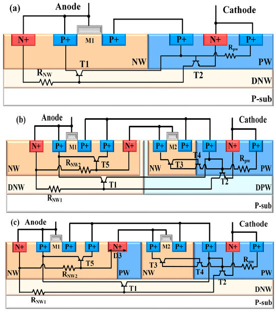
Figure 1.
Cross-sections and internal equivalent circuits of (a) PMOS-SCR, (b) DPMOS-SCR, and (c) ODPMOS-SCR.
Aiming to reduce the EOS breakdown and leakage current risk in DPMOS-SCR, we embedded a left P-well (PW) and repositioned the N+ region across the left NW and PW. The embedded PW introduces an additional space charge region that improves holding voltage (Vh), while the relocated N+ region reduces trigger voltage. This optimized structure, designated as ODPMOS-SCR, maintains strong ESD/EOS discharge capability while achieving lower snapback voltage. Although sharing a similar equivalent circuit with DPMOS-SCR, ODPMOS-SCR introduces an additional SCR path through parasitic transistors T3 and T4, attributed with discharging the ESD/EOS current. When the additional SCR path conducts, transistors T3 and T4 operate in amplification state, where the current gain βT3 and βT4 meet the operation condition defined by Formula (2). By narrowing the T3’s base region width, the increased βT3 value effectively enhances the current conduction capability of the additional SCR. These structural modifications reduce the turn-on resistance, thereby improving voltage clamping ability.
Figure 2 illustrates the typical electrical characteristics of the ESD/EOS protection design window. The snapback curve represents the current–voltage (I-V) characteristics under TLP stresses. Here, VDD represents the normal operating voltage of the protected chip, IDD corresponds to the operating current of internal chips, and BVOX defines the gate-oxide breakdown voltage of the fabrication process. I-V curves highlight three key points of the ESD/EOS protection: (1) Triggering point: defined by the trigger voltage (Vt1) and trigger current, indicates the turn-on threshold of protection devices. When the stressed ESD/EOS pulse exceeds Vt1 and the breakdown voltage (BV), the protection device transitions from an off to an on state. (2) Holding point: the minimum clamping voltage (Vh) after device turn-on, where latch-up risk exists when clamping voltage (Vc) decreases below VDD and trigger current is less than IDD. (3) Failure point: determined by the BVOX second breakdown current (It2), representing the irreversible device failure.
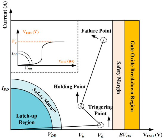
Figure 2.
Typical ESD/EOS protection design window.
2.2. Operation Mechanism
When the electrical pulse with a low amplitude is stressed on VDD and VSS pads, the operating schematics of the ODPMOS-SCR are illustrated as the equivalent circuit shown in Figure 3. Here, VDD and VSS represent the power and ground connections of the protected circuit. Both left PMOS (M1) and right PMOS (M2) are initially triggered, enhancing the current flow through resistance RPW. Meanwhile, the transistor PNP (T5) will also be triggered to enhance the surface discharge capacity of the device. When the voltage dropping on RPW and RNW1 exceeds 0.7 V, the first SCR conduction path constructed by transistors T1 and T2 turns on, due to the positive feedback effect of the compound transistor and the assistant triggering effect of the RNW1. As the pulse amplitude and duration increase beyond a certain threshold, the second SCR conduction path constructed by transistors T3 and T4 turns on. The second SCR path exhibits slower turn-on characteristics compared to the first SCR conduction path because of the series well resistant RNW2 and the absence of the bias resistance-assisted triggering effect.
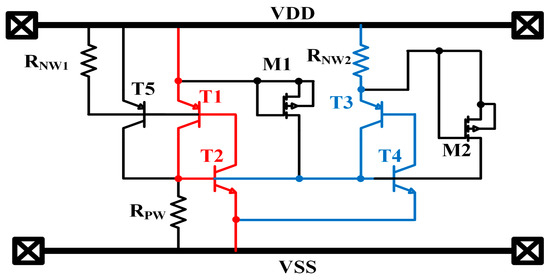
Figure 3.
Equivalent circuits of ODPMOS-SCR.
The electrical mechanism of the ODPMOS-SCR stressed by a series of electrical transient pulses was simulated by TCAD tools. Figure 4 illustrates current density distributions under the different electrical pulses. When the transient pulse is small, both PMOS transistors turn on rapidly with minimal current, as indicated by the auto-generated black arrow line in Figure 4a. When the transient pulse increases, all parasitic structures, including the PMOS, PNP, and SCR paths, turn on to discharge substantial current, as indicated by auto-generated black arrow lines in Figure 4b. Simulation results agree well with the above-mentioned operating mechanism, demonstrating the rapid triggering by dual PMOS transistors and efficient surface current conduction. The achieved current up to 2.0 × 10⁵ A/cm2 effectively confirms the strong current discharge ability under EOS stress.
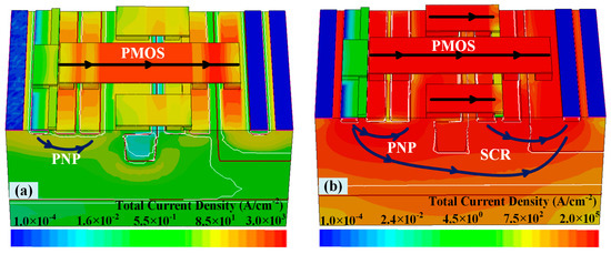
Figure 4.
A 3D simulation of the current density distribution (a) before and (b) after turning on ODPMOS-SCR.
Two-dimensional (2D) TCAD simulations were also conducted to analyze ODPMOS-SCR stressed by electrical transient pulses with varying durations of 10 ns, 100 ns, and 10 μs at constant voltage. Figure 5 reveals the sequential activation of device components: PMOS and PNP triggering, followed by first and second SCR paths. For the short-duration pulse, the first SCR conduction path is mainly effective for discharge ESD current. For the longer-duration pulse, both SCR paths conduct simultaneously for discharging surge current. These 2D simulation results complement the 3D analysis shown in Figure 5, providing detailed insights into the turn-on order of ODPMOS-SCR.
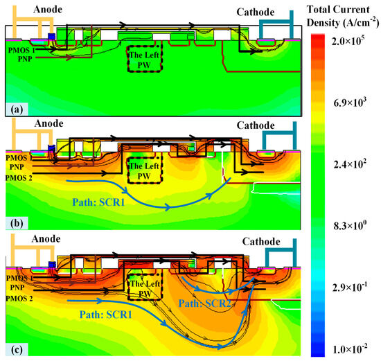
Figure 5.
A 2D simulation of the current density distribution of ODPMOS-SCR at different times: (a) t = 10 ns, (b) t = 100 ns, and (c) t = 10 μs.
The electrostatic potential and electric field distributions of experimental devices are also studied by physical models and TCAD simulations. Device physical models are characterized by Formulas (3) and (4) [17], where the electric field (E) and electrostatic potential (V) correlate with the net doping concentrations NA, ND, and space charge depletion width x under varying electrical stress conditions. In the simulation, the value of NA and ND ranges from 1019 to 1020 μm−3.
TCAD simulations of the E and V distribution are shown in Figure 6 and Figure 7. Both E and V increase with the pulse amplitude until reaching 9.3 V, where E approaches the critical breakdown field. The experimental device then turns on, leading to V with minimal decrease under increased EOS stress and thus obtaining a stable voltage clamping ability. The deep analysis of the voltage clamping capability was conducted by studying the ODPMOS-SCR structure without the embedded left PW, marking as ODPMOS-SCR_WO.
where q represents the electric charge, k denotes the Coulomb constant, VBi indicates the built-in potential across the depletion region, and Vb describes the applied bias voltage.
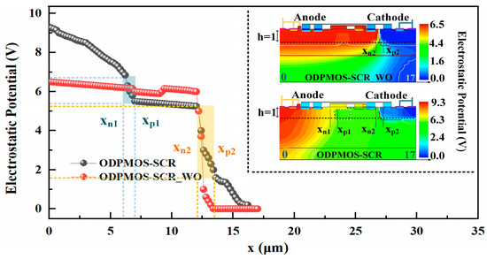
Figure 6.
Simulated electrostatic potential distribution curves of ODPMOS-SCR_WO and ODPMOS-SCR.
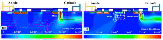
Figure 7.
Simulated electrical field of (a) ODPMOS-SCR_WO and (b) ODPMOS-SCR.
As shown in Figure 6, the internal distribution under the changing V with the lateral distance x is extracted along the surface-to-bulk depth h = 1 shown in the Figure 6 inset. ODPMOS-SCR_WO exhibits higher overshoot voltage than ODPMOS-SCR, increasing from 6.5 to 9.3 V. Except for the space charge region between xn2 and xp2, ODPMOS-SCR with the left PW exhibits an additional depletion region between xn1 and xp1, resulting in the voltage clamping point shift from the cathode to the anode. The enhanced voltage capability originates from an additional space charge depletion region caused by inserting the left PW, as verified by the electric field simulation in Figure 7. An elevated electric field appears around the left PW, as shown in Figure 7b, leading to the increased BV and Vt1. By combining the results in Figure 6, ODPMOS-SCR demonstrates two distinct voltage drops: 1.8 V for x increasing from 5.6 to 7 μm and 3.4 V for x increasing from 12.2 to 13.6 μm, confirming the space charge region’s significant contribution to the voltage clamping performance.
DC I-V characteristics of PMOS-SCR, DPMOS-SCR, and ODPMOS-SCR were obtained from simulation, as shown in Figure 8. DPMOS-SCR exhibits a slightly higher BV than PMOS-SCR, due to increased anode–cathode spacing. Moreover, the incorporation of left PW in ODPMOS-SCR significantly enhances BV from 6.8 V to 9.4 V. These electrical characteristics agree well with physical model predictions and simulated electric field distributions.
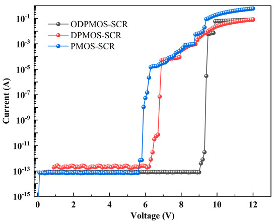
Figure 8.
Simulated DC I-V characteristic curves of PMOS-SCR, DPMOS-SCR, and ODPMOS-SCR.
3. Device Measurement and Analysis
The proposed DPMOS-SCR and ODPMOS-SCR devices with the same width of 170 μm were fabricated and verified in a 0.18-μm BCD (Bipolar-CMOS-DMOS) process. The ESD characteristics were measured by sweeping DC from 0 to 10 V and testing TLP with a 10 ns rise time and 100 ns width ESD pulses. The electrical characteristic curves of experimental devices are shown in Figure 9 and Figure 10.
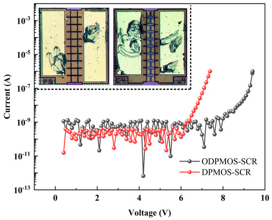
Figure 9.
DC I-V characteristic curves of ODPMOS-SCR and DPMOS-SCR.
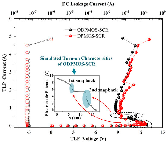
Figure 10.
TLP I-V curves of ODPMOS-SCR and DPMOS-SCR.
DC I-V characteristics measured by the precise semiconductor parameter analyzer reveal that DPMOS-SCR exhibits a leakage current transition from nanoampere to microampere scale at 6.8 V bias voltage, followed by turning on the device with a low resistance. By incorporating the left PW in ODPMOS-SCR, BV increases from 7.0 V to 9.2 V. These measured DC I-V characteristics closely align with simulation results presented in Figure 8.
The ESD characteristics of the ODPMOS-SCR and DPMOS-SCR were also investigated by the TLP test system. The trigger voltage and holding voltage, as well as the It2 of both devices, change unremarkably. The measured trigger and holding states agree well with the simulation results shown in Figure 6. The devices exhibit dual snapback characteristics, matching simulation results in the Figure 10 inset, with a small snapback voltage of 2.5 V at 0.5 A holding current. The experimental devices achieve higher It2 and holding voltage through dual snapback states, enhancing the voltage clamping performance. In addition, by increasing the channel length and optimizing the W/L, the Vt1 can be further reduced to meet the protection design window requirements of 5–15 V applications.
The ESD characteristics of ODPMOS-SCR were also further improved by optimizing the finger number (F). As is shown in Figure 11, increasing F from 1 to 3 improves the It2 of ODPMOS-SCR from 4.5 to 13.0 A, demonstrating the good linearity and current conduction uniformity, due to the introduced dual PMOS and SCR conducting paths. Thus, the superior current-conducting capability of ODPMOS-SCR enables further investigation of EOS protection.
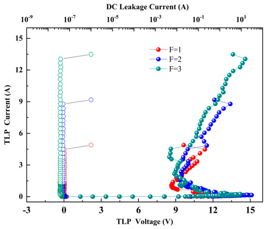
Figure 11.
TLP I-V curves of ODPMOS-SCR with different F.
EOS characteristics of ODPMOS-SCR were evaluated using an 8/20 μs surge test system, with an 8 μs rise time and a 20 μs pulse duration. The voltage–time (V-t) characteristics in Figure 12a show the maximum endurance voltage with an overshoot peak of 15.4 V, while Figure 12b demonstrates the stable clamping voltage at 5.9 V, confirming effective voltage clamping and latch-up immunity. The current–time (I-t) curve in Figure 12c reveals the peak surge current (IPP) reaching 3.7 A, surpassing comparable devices with different circuit configurations.
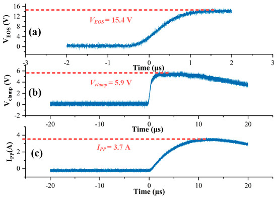
Figure 12.
The EOS characteristic curves of ODPMOS-SCR: (a) EOS voltage (b) clamping voltage (c) pulse peak current.
Current conduction uniformity and IPP enhancement were investigated by varying F from 1 to 3 in fabricated ODPMOS-SCR devices. As shown in Figure 13, the EOS characteristics show that IPP increases from 2.5 to 3.7 A with the increasing F, achieving optimized current conduction at F = 2. However, the non-uniform conductivity characteristics of ODPMOS-SCR at F = 3 require further investigation and optimization.
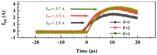
Figure 13.
The EOS characteristic curves of ODPMOS-SCR with different F.
A comparison of key device parameters under ESD and EOS stress is presented in Table 1. Compared to the reported SLVTSCR [18] and DMTSCR [19] devices with similar trigger and holding characteristics, the DPMOS-SCR and ODPMOS-SCR series demonstrate a smaller snapback voltage, turn-on resistance (Ron), and larger It2. These superior ESD characteristics make them suitable for EOS protection applications. ODPMOS-SCR achieves remarkable performance metrics with It2 of 8.8 A and IPP of 3.5 A within a compact chip area of 170 × 21 × 2 μm2, making it promising for the ESD/EOS co-protection.

Table 1.
ESD/EOS electrical characteristics of device.
4. Conclusions
This work presents novel DPMOS-SCR and ODPMOS-SCR structures with comprehensive mechanism analysis based on a 0.18-μm BCD process. The strategic embedding of middle P-well in DPMOS-SCR enhances the voltage clamping capability, minimizing Ron to 0.9 Ω and snapback voltage to 2.5 V. Dual PMOS and SCR conduction paths enable the high It2 and peak pulse current, reaching It2 of 8.8 A and IPP of 3.5 A, resulting in the strong ESD robustness and EOS current-conducting ability. The ODPMOS-SCR suited for the 5–15 V ESD/EOS protection design window exhibits superior performance with a BV of 9.4 V, a Vt1 of 14.2 V, and a Ron of 0.4 Ω under both ESD and EOS testing, validating its effectiveness for applying to the monolithic ESD/EOS protection.
Author Contributions
Conceptualization, methodology, validation, and writing—original draft preparation, H.L. and J.L. (Jianfeng Li); investigation and data curation, H.L. and J.L. (Jianfeng Li); writing—review and editing, J.L. (Jianfeng Li), H.L., J.L. (Junliang Liu), J.S., D.W. (Dejin Wang), F.W. and D.W. (Dong Wang); funding acquisition, J.L. (Junliang Liu). All authors have read and agreed to the published version of the manuscript.
Funding
This work is supported by the Joint Project of Yangtze River Delta Community of Sci-Tech Innovation (grant No. 2022CSJGG0400); in part by the Natural Science Foundation of Jiangsu Province of China (grant No. BK20231038); and in part by the Fundamental Research Funds for the Central Universities (grant No. JUSRP123062).
Data Availability Statement
Data are contained within the article.
Conflicts of Interest
Authors Jun Sun and Dejin Wang were employed by the company Process Development Department, CSMC Inc. Authors Fang Wang and Dong Wang were employed by the company Wuxi ETEK Microelectronics Co., Ltd. The remaining authors declare that the research was conducted in the absence of any commercial or financial relationships that could be construed as a potential conflict of interest.
References
- Chen, J.T.; Lin, C.Y.; Ker, M.D. On-chip ESD protection device for high-speed I/O applications in CMOS technology. IEEE Trans. Electron Devices 2017, 64, 3979–3985. [Google Scholar] [CrossRef]
- Lin, C.Y.; Wu, P.H.; Ker, M.D. Area-efficient and low-leakage diode string for on-chip ESD protection. IEEE Trans. Electron Devices 2016, 63, 531–536. [Google Scholar] [CrossRef]
- Du, F.; Jiang, G.; Huang, M.; Zou, K.; Hou, F.; Song, W.; Liu, J.; Xiong, X.; Hou, L.; Liu, Z.; et al. Investigation and suppression of holding voltage deterioration in multifinger SCR for robust high-voltage ESD engineering. IEEE Trans. Electron Devices 2021, 68, 6338–6343. [Google Scholar] [CrossRef]
- Zeng, J.; Dong, S.R.; Liou, J.J.; Han, Y.; Zhong, L.; Wang, W.H. Design and analysis of an area-efficient high holding voltage ESD protection device. IEEE Trans. Electron Devices 2015, 62, 606–614. [Google Scholar] [CrossRef]
- Han, A.; Liu, Y.; Liu, Z.W.; Luo, X. Compact wideband millimeter-wave ESD protection device with transformer-embedded DCSCR. IEEE Electron Device Lett. 2023, 44, 1531–1534. [Google Scholar] [CrossRef]
- Shen, Y.S.; Ker, M.D. The impact of holding voltage of transient voltage suppressor (TVS) on signal integrity of microelectronics system with CMOS ICs under system-level ESD and EFT/burst tests. IEEE Trans. Power Electron. 2021, 68, 2152–2159. [Google Scholar] [CrossRef]
- Zhang, C.R.; Zeng, X.; Zhou, L.; Mao, J.F. Protection effects using transient voltage suppressor diodes based circuits under high-power microwave pulses. IEEE Trans. Electromagn. Compat. 2021, 63, 2058–2064. [Google Scholar] [CrossRef]
- Dai, S.H.; Lin, C.J.; King, Y.C. Leakage suppression of low-voltage transient voltage suppressor. IEEE Trans. Electron Devices 2008, 55, 206–210. [Google Scholar] [CrossRef]
- Huang, X.Z.; Liou, J.J.; Liu, Z.W.; Liu, F.; Liu, J.Z.; Chen, H. A new high holding voltage dual-direction SCR with optimized segmented topology. IEEE Electron Device Lett. 2016, 37, 1311–1313. [Google Scholar] [CrossRef]
- Qi, Z.; Qiao, M.; Liang, L.; Zhang, F.; Zhou, X.; Cheng, S.; Zhang, S.; Lin, F.; Sun, G.; Li, Z.; et al. Novel silicon-controlled rectifier with snapback-free performance for high-voltage and robust ESD protection. IEEE Electron Device Lett. 2019, 40, 435–438. [Google Scholar] [CrossRef]
- Song, W.; Chen, R.; Tong, Z.; Hou, F.; Du, F.; Liu, Z.; Liu, H. Robust silicon-controlled rectifier with high-holding voltage for on-chip electrostatic protection. IEEE Trans. Electron Devices 2022, 69, 696–703. [Google Scholar] [CrossRef]
- He, L.F.; Salcedo, J.A.; Parthasarathy, S.; Hajjar, J.; Sundaram, K. A New Low-Capacitance High-Voltage-Tolerant Protection Clamp for High-Speed Applications. IEEE Trans. Electron Devices 2020, 67, 3030–3034. [Google Scholar] [CrossRef]
- Yang, Z.; Xu, J.; Fu, D.; Zhang, Y.; Zhang, Y.; Yang, Y.; Yu, N. New power clamp circuit for concurrent ESD and surge protections. IEEE Trans. Electron Devices 2023, 70, 4538–4546. [Google Scholar] [CrossRef]
- Bae, B.; Kim, J. A low-voltage microwave plasma ionizer with reduced electric overstress due to displacement current coupling from a high-AC voltage source. IEEE Trans. Electromagn. Compat. 2021, 63, 1501–1511. [Google Scholar] [CrossRef]
- Tsovilis, T.E.; Hadjicostas, A.Y.; Staikos, E.T.; Peppas, G.D. An experimental methodology for modeling surge protective devices: An application to DC SPDs for electric vehicle charging stations. IEEE Trans. Ind. Appl. 2024, 60, 1645–1655. [Google Scholar] [CrossRef]
- Radulovic, V.M.; Miljanic, Z.V. Effects of built-in varistors with low protection voltages on surge protection performances in low-voltage AC power systems. IEEE Trans. Electromagn. Compat. 2020, 62, 933–946. [Google Scholar] [CrossRef]
- Gharekhanlou, B.; Khorasani, S. Current–voltage characteristics of graphane p-n junctions. IEEE Trans. Electron Devices 2010, 57, 209–214. [Google Scholar] [CrossRef]
- Liang, H.L.; Zhu, L.; Gu, X.F. A dual-MOS-triggered silicon-controlled rectifier for high-voltage ESD protection. IEEE J. Emerg. Sel. Top. Power Electron. 2021, 9, 6293–6299. [Google Scholar] [CrossRef]
- Dong, S.R.; Jin, H.; Miao, M.; Wu, J.; Liou, J.J. Novel capacitance coupling complementary dual-direction SCR for high-voltage ESD. IEEE Electron Device Lett. 2012, 33, 640–642. [Google Scholar] [CrossRef]
Disclaimer/Publisher’s Note: The statements, opinions and data contained in all publications are solely those of the individual author(s) and contributor(s) and not of MDPI and/or the editor(s). MDPI and/or the editor(s) disclaim responsibility for any injury to people or property resulting from any ideas, methods, instructions or products referred to in the content. |
© 2025 by the authors. Licensee MDPI, Basel, Switzerland. This article is an open access article distributed under the terms and conditions of the Creative Commons Attribution (CC BY) license (https://creativecommons.org/licenses/by/4.0/).