Article

Effects of Wide Bandgap Devices on the Inverter Performance and Efficiency for Residential PV Applications

by
Saleh S. Alharbi
1,*,
Salah S. Alharbi
1,
Abdullah Bubshait
2,
Hisham Alharbi
3 and
Abdulaziz Alateeq
4
1
Department of Electrical Engineering, Faculty of Engineering, Al-Baha University, Alaqiq 65779, Saudi Arabia
2
Electrical Engineering Department, College of Engineering, King Faisal University, Al-Ahsa 31982, Saudi Arabia
3
Department of Electrical Engineering, College of Engineering, Taif University, Taif 21944, Saudi Arabia
4
Department of Electrical Engineering, College of Engineering, University of Ha’il, Ha’il 2240, Saudi Arabia
*
Author to whom correspondence should be addressed.
Electronics 2025, 14(6), 1061; https://doi.org/10.3390/electronics14061061
Submission received: 2 February 2025 / Revised: 28 February 2025 / Accepted: 4 March 2025 / Published: 7 March 2025
(This article belongs to the Special Issue Power Electronic Circuits and Systems for Emerging Applications)

Abstract

:
With power demands continuously growing, the penetration of renewable energy resources, particularly solar photovoltaic (PV) systems, across the residential sector has been extensive. A voltage source inverter (VSI) is the key element for efficiently processing energy conversion and connecting PV systems to home loads or utility grids. The operation of this inverter relies heavily on power-switching devices, which suffer from larger power losses due to the conventional semiconductors used based on silicon (Si) material. The new materials of wide bandgap (WBG) semiconductors, for example, gallium nitride (GaN) and silicon carbide (SiC), provide remarkably distinct characteristics of semiconductor devices to minimize power loss and boost the inverter’s operational capabilities. This research paper assesses the effects of integrating SiC-MOSFET devices into VSIs in order to improve the switching behavior and efficiency level. An experimental double-pulse testing (DPT) circuit was configured and set up for investigating the switching characterization of SiC-MOSFETs compared to the widely used Si-IGBTs. Under various operating circumstances, the switching behavior of two different types of power transistors was tested while their turning-on and turning-off losses were measured. The VSI based on SiC and Si transistors was simulated to examine the performance of the inverter. The results reveal that incorporating SiC-MOSFETs into the VSI substantially enhances the switching operation and reduces total power losses while increasing the efficiency compared to the inverter based on Si-IGBTs.

1. Introduction

Among various renewable energy sources, the penetration of solar photovoltaic (PV) systems, especially across the power distribution network, has been extensive, substantially due to the appealing advantages of clean and sustainable energy along with affordable technology [1,2]. In 2021, the Photovoltaic Power Systems Programme (PVPS) report released by the International Energy Agency (IEA) showed a major increase in the overall global capacity of installed PV systems [3,4]. This capacity is reported at approximately 1160 GWp with a yearly installation rate of 220 GWp [5]. Most of these PV systems have been rapidly utilized and installed in the residential sector while there are an increasing number of PV rooftop systems implemented in commercial premises [6,7]. In PV systems, voltage source inverters (VSIs) play a vital role in processing energy conversion and regulating the voltage between PV arrays combined with battery banks and the load/utility grid [8,9]. Therefore, VSIs are widely adopted in grid-tie PV systems [10,11].
In VSIs, a high level of reliability and efficiency along with fast switching performance and low cost are major priorities in obtaining power grid parity [12,13,14]. These priorities are essential in manufacturing the power inverters for on-grid PV systems [15,16,17]. Currently, the vast majority of VSI topology is composed of silicon (Si) switching devices and passive elements, such as capacitors and inductors [18,19]. However, VSIs struggle with drastic conduction and switching losses caused by Si-based semiconductor devices, leading to a marked drop in the inverter efficiency as these semiconductor transistors are core parts of processing energy conversion [20,21]. Moreover, most VSIs in grid-connected PV systems rely heavily on commonly used Si-based power devices [22,23]. These inverters face crucial challenges in improving their operating capabilities because the exacting Si-based switches are fabricated using Si technology, which is reaching its physical and theoretical limits [24,25]. It is worth mentioning that the limitations of Si-based transistors reflect high voltage stress across switching devices with limited voltage ratio conversion [26,27]. Consequently, power inverters with Si-based devices are unable to achieve higher energy efficiency and better switching performance when employed in grid-tied PV systems.
To overcome the abovementioned challenges, many methodologies have been applied to develop inverter topologies, such as multilevel techniques [28,29]. In the meantime, numerous studies have proposed different sophisticated control strategies to enhance the inverter performance [30,31,32]. Although these solutions show good outcomes for the power inverter, the increasing levels of cost, size, and complexity are still critical constraints for grid-connected PV systems. Recently, academic researchers have produced a large number of valuable studies regarding emerging new materials of wide bandgap (WBG) semiconductors, for example, silicon carbide (SiC) and gallium nitride (GaN) for PV inverters [33,34,35,36]. WBG technology has great potential, allowing power devices to operate effectively because of the distinct material characteristics compared to the currently used Si materials [37,38,39]. These outstanding material properties include a wider energy gap, larger electric field, higher thermal conductivity, faster electron velocity, and greater melting point. As a result of these distinct properties, WBG-based devices are capable of working efficiently in high-voltage operation, in high-temperature ambiance, and with fast switching frequency [40,41,42].
In addition, several studies, as demonstrated in [43,44,45,46], have reported merging WBG-based switches, such as SiC metal-oxide-semiconductor-field-effect transistors (MOSFETs) and GaN field-effect-transistors (FETs), into grid-connected PV inverters. These studies have revealed that the efficiency and performance of PV inverters are markedly improved by replacing the traditional Si-based switches with SiC and GaN counterparts due to reduced conduction and switching losses along with minimized size and weight of the passive elements. Among WBG semiconductors, SiC-MOSFETs feature high operating capabilities of switching frequency, ability to operate at high temperature, and blocking voltage [47,48,49]. For Si-based devices, insulated-gate-bipolar-transistors (IGBTs) are suitable transistors for high-power conversion systems with a low-medium switching frequency because they consist of a combination of a MOSFET with a bipolar switch at a large input impedance and high current density [50,51,52].
Various articles, e.g., [53,54,55], have investigated the integration of SiC-MOSFET switches on the inverter level and compared them to Si-based switches. Some published works, e.g., [56,57,58], have evaluated the power loss calculation of three-phase VSI topology based on SiC-MOSFET along with Si-IGBT devices in different working situations. Their experimental outcomes reveal considerably reduced conduction and switching losses by emerging SiC-MOSFETs. A number of studies, e.g., [59,60,61], demonstrated that the switching behavior of SiC-MOSFETs and Si-IGBTs incorporated into power inverters is significantly enhanced against the switching behavior of Si-IGBTs because of the superior materials of WBG technology. In [62,63,64,65], the power loss and efficiencies of high-voltage SiC-MOSFET and Si-IGBTs incorporating antiparallel SiC-diodes are considered and evaluated for high-power inverters.
Although the articles and studies mentioned above show that merging SiC-MOSFETs and Si-IGBTs can result in power inverters having better performance and higher efficiency, there are some challenging issues, such as complicated gate-drive circuits, high device cost, and large parasitic parameters, which still require urgent resolution to achieve all the advantages of SiC-IGBTs. However, there is a clear knowledge gap that exists in using the low-medium voltage level 900-V SiC-MOSFETs and Si-IGBTs with the same gate driver and package for power inverters. Furthermore, there is inadequate practical information related to the critical challenges of Si-IGBTs and SiC-MOSFETs, including an extended tail current at the turn-off transition, major ringing oscillation during the turn-on period, and limited switching frequency. Therefore, traditional Si-IGBTs and SiC-MOSFETs still need further evaluation on the inverter level. The objective of this article is to narrow the previously provided knowledge gap by investigating experimentally the behavior changes as well as analyzing the switching losses of SiC-MOSFETs and Si-IGBTs in various working circumstances through the DPT circuit. In PLECS software, inverters with two different devices are simulated based on the experimental results, and along with the electrical parameters of the device datasheet, have been applied to assess the power loss and efficiency under identical operating circumstances.
This paper is organized as follows: Section 2 provides a concise overview of PV systems, including grid-connected and stand-alone systems, and of the VSI power inverter. Section 3 provides an analysis of the device and inverter losses. Section 4 highlights the experimental setup of the device characterization. Section 5 shows the dynamic characterization for the Si-IGBT and SiC-MOSFET, analyzing the energy loss of each transistor in varied working situations. Section 6 provides an evaluation of the inverter performance based on SiC-MOSFET and Si-IGBT switches to determine the total losses and energy efficiency. Finally, the conclusions regarding the research findings are presented in Section 7.

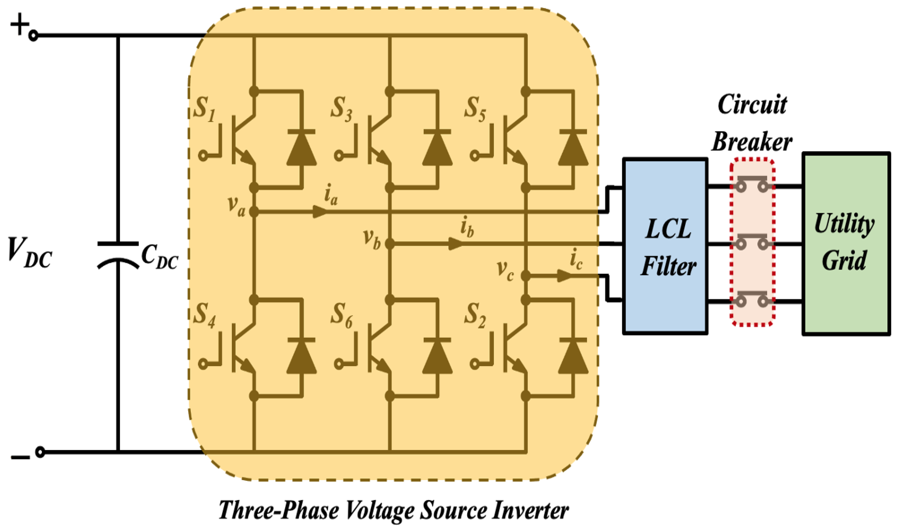
2. Power Inverter for Grid-Connected PV System

2.1. PV System

The installation of rooftop PV conversion systems can be categorized primarily based on the connection patterns of the solar systems into stand-alone (off-grid) and grid-connected (on-grid) systems. Figure 1 illustrates the main differences between the two systems. The stand-alone PV system is an operationally self-contained solar PV system disconnected from the grid as this system is commonly used in remote and rural locations. The main drawback of the stand-alone PV system is the indispensable need for large battery energy storage elements along with a diesel generator. Moreover, this system can be highly expensive to maintain when powering home electrical appliances for a long time. On the other hand, grid-connected PV systems are implemented as PV arrays which are tied to the local power grid through the power inverter. This system operates to provide most house appliances during the daytime while it is still connected to the utility electricity grid. During the night, the load can be powered by the battery storage or local grid. This means that the on-grid PV system features bidirectional power flows from the main grid based on the sunlight conditions and electric load demands. The major advantages of grid-tied PV systems is that they are reliable, cost-effective, and operationally uncomplicated. As a result, grid-connected PV systems are much more frequently implemented in residential buildings compared with stand-alone PV systems.

2.2. Power Inverter

Power electronics, such as inverters, are the most crucial pieces of equipment integrated into grid-connected PV systems in order to process energy conversion efficiently under various operating conditions. The inverter is a power conversion device that can convert direct current (DC) electricity from the source to alternative current (AC) electricity in order to be supplied to the utility grid or to meet household loads. Power inverters are four-quadrant converters with a bidirectional output current and bipolar output voltage. This paper considers a large residential application and its energy consumption, modeling and implementing a three-phase VSI inverter. Figure 2 depicts a schematic diagram of the three-phase VSI inverter tied to the utility network. Several articles have presented the model equations and analysis of the three-phase two-level VSI inverter, including [66,67,68].

3. Inverter Power Loss Analysis

This section explains the calculation of different power losses for the two used transistors as these transistors are considered crucial parts of the VSI inverter. Ordinarily, the power dissipation that occurs in the transistors can be split into two major segments: static and dynamic losses. The static loss comprises cut-off and conduction losses, whereas the dynamic loss consists of switching losses during the time-on and time-off periods [69]. Commonly, the loss of cut-off for SiC and Si devices can be disregarded because of the low leakage current [70]. It is worth mentioning that the electrical characteristics of semiconductor devices, such as the breakdown voltage, continuous current, and on-state resistance, play a large role in quantitative power loss. Figure 3 depicts the ideal waveforms of the switching device, including conduction and switching losses.

3.1. Conduction Loss

Conduction loss occurs when a power transistor or freewheeling diode turns on and conducts current. The power dissipation in conduction status is calculated by multiplying the on-state current and voltage. The conduction loss occurs when the current streams via the transistors. This loss results from the dynamic on-resistance ( R D S ( o n ) ) so the physical size of the semiconductor device materials can be a major influence on the conduction loss. Also, the breakdown voltage can be positively proportional to the junction temperature. The average conduction loss ( P c o n d ) of the semiconductor for one switching cycle ( T s w ) is computed as follows:
P c o n d = 1 T s w t 3 t 6 [ v ( t ) i ( t ) ] d t
To link the datasheet parameters to the above equation, the equation is linearized to be more suitable for on-state loss equations for semiconductor power devices. Therefore, the conduction loss for different power devices can be determined mathematically as follows:
P c o n d ( M O S F E T ) = I R M S 2 R D S ( o n )
P c o n d ( I G B T ) = V C E 0 I R M S + I R M S 2 R 0
P c o n d ( D i o d e ) = V D 0 I R M S + I R M S 2 R D 0
where I R M S is the root-mean-square current. V C E 0 is the on-state threshold voltage between the collector and emitter of the Si-IGBT, while R 0 is the on-state resistance, which is temperature-dependent. V D 0 and R D 0 are the dynamic on-state characteristics of the voltage and resistance for the diode.

3.2. Switching Energy Loss

The switching loss of transistors that results from the turning-on and turning-off periods is categorized as the energy loss. Both the conducting current flowing through the semiconductor device and the voltage drop over this device are considerably higher than zero during a commuted interval, leading to a major instantaneous power loss. These losses are computed by integrating the multiplication of the current and voltage waveforms during the transition interval. Energy loss basically results when the semiconductor is switching on and off. Thus, the switching frequency ( f s w ) considerably affects the energy loss. Furthermore, the physical material of the semiconductor devices plays a large role in the switching loss because of their intrinsic parasitic capacitance. The traditional Si fast recovery diode (FRD) suffers from recovery losses during turn-off transiently because of a large reverse recovery time, causing momentary non-zero voltage and reverse current. Therefore, the SiC diode is used in this study. The energy losses for turning-on ( E o n ) and turning-off ( E o f f ) periods can be determined with the following equation:
E o n = t 1 t 3 [ v ( t ) i ( t ) ] d t
E o f f = t 6 t 8 [ v ( t ) i ( t ) ] d t
The switching loss for the implemented transistors and diodes can be computed as follows:
P s w ( M O S F E T ) = ( E o n + E o f f ) f s w
P s w ( I G B T ) = ( E o n + E o f f ) f s w
P s w ( D i o d e ) = ( E o f f ) f s w

3.3. Total Power Loss of the Inverter

The conduction loss along with the switching energy losses that result from the power transistors are computed to determine the total losses of the inverter because these losses significantly affect the switching performance and efficiency level. Various modulation methods are subjected to two-level three-phase VSIs. The objectives of these methods are reducing harmonic distortion and minimizing switching power loss. The most-used modulation strategies for VSIs are space vector pulse modulation (SVPWM) and sinusoidal pulse width modulation (SPWM). This research implements and analyzes the SPWM modulation (m) approach for the PV power inverter. Considering the nominal parameters based on the datasheet, the switching power loss is normalized to be compatible with the inverter application. According to [69,71,72,73,74], the conduction and switching losses for different semiconductors employed in the VSI inverter can be expressed as follows:
P c o n d ( M O S F E T ) = [ 1 8 + m cos ( θ ) 3 π ] [ R D S ( o n ) I p k 2 ]
P c o n d ( I G B T ) = [ 1 2 π + m cos ( θ ) 8 ] [ V C E 0 I p k ] + [ 1 8 + m cos ( θ ) 3 π ] [ R 0 I p k 2 ]
P c o n d ( D i o d e ) = [ 1 2 π + m cos ( θ ) 8 ] [ V D 0 I p k ] + [ 1 8 m cos ( θ ) 3 π ] [ R D 0 I p k 2 ]
P s w ( M O S F E T ) = [ ( E o n + E o f f ) f s w π ] [ 2 I o u t I N O M ] [ V D C L i n k V N O M ]
P s w ( I G B T ) = [ ( E o n + E o f f ) f s w π ] [ 2 I o u t I N O M ] [ V D C L i n k V N O M ]
P s w ( D i o d e ) = [ ( E o f f ) f s w π ] [ 2 I o u t I N O M ] [ V D C L i n k V N O M ]
where I o u t and I N O M are the RMS output current and nominal rated current of the power switches. V D C L i n k is the voltage across the DC-Link, while V N O M is the datasheet dynamic line voltage.
In general, the VSI topology consists of three phases and each of the three phases contains the same two switching power devices with antiparallel diodes, as presented in Figure 2. The total power loss ( P l o s s ) for the two-level three-phase VSI inverter using the SPWM technique is calculated as follows:
P l o s s = 6 [ P c o n d ( M O S F E T o r I G B T ) + P c o n d ( D i o d e ) + P s w ( M O S F E T o r I G B T ) + P s w ( D i o d e ) ]

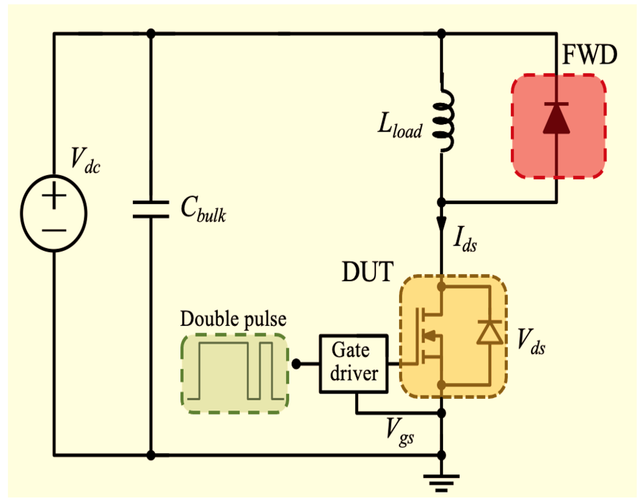
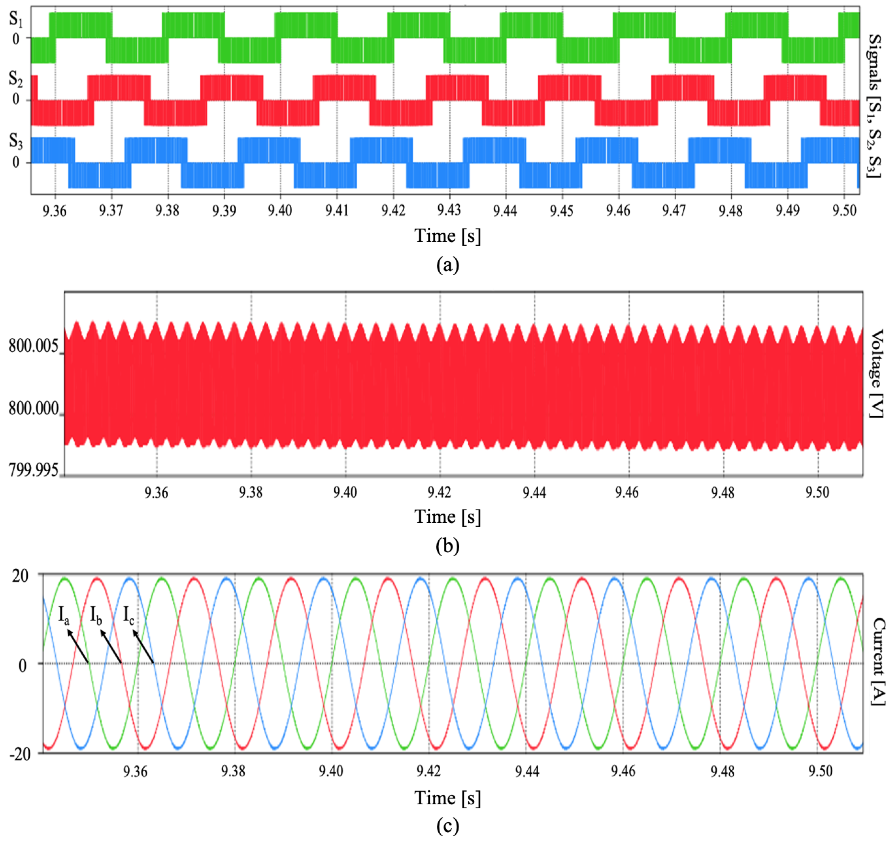
4. Experimental Setup

This section describes the comprehensive switching performance of two device technologies under a hard-switching environment, enabling power electronics designers to determine the optimal driving condition and estimate the energy loss more accurately. The characterizations and switching loss mechanism of the Si-IGBT and SiC-MOSFET devices are investigated under the same hardware setup. The simplified double-pulse test (DPT) used for dynamic characterizations is illustrated in Figure 4. A high-speed IC gate driver (1ED160I12AH) is utilized for power devices with an adequate peak current and a variable voltage range. As shown in Figure 4, typical double-pulse signals are used to show the characteristics of the device under the test (DUT). The gate signal consists of two pulses with adjustable pulse widths that are generated by the function generator model (3300B). The positive and negative gate voltages are provided for both power devices to ensure that they can operate safely at faster switching speeds [75]. Furthermore, the freewheeling diode is a SiC-Schottky diode inserted into the test circuit and placed antiparallel to a clamped inductive load. The two power devices are chosen such that they have similar voltage-blocking capability, continuous current rating, and commercial TO-247 package. All of the main devices are employed as bottom-side switches of the test circuit. Table 1 provides the essential parameters of the selected power devices.
The process of testing the device performance and acquiring loss information is illustrated in Figure 5. To calculate the energy loss of the main switching device, the product value of the switch voltage and current is defined over a specific time interval, and the integration of the outcomes is taken as expressed in Equations (5) and (6) [76]. The selected digital oscilloscope, model (DPO3014), is used to capture the switching behavior and obtain the energy losses. An adequate bandwidth current sensor is used to measure the current path of different devices in the DUT. A high-voltage differential probe (P5200A) is utilized to record the switch voltages of each power device. Due to the rapid rise and fall times of SiC power devices, a high bandwidth with a wide dynamic range is essential for the measurement methods to precisely capture the dynamic performance and energy losses for each device. Table 2 shows the detailed instruments of the DPT setup.
In practical measurement, the influence of delay variation among the measured voltage and current is a critical consideration, especially when evaluating the energy loss and inverter efficiency. This will inhibit the switching waveforms and result in timing misalignment in the measurement of switching losses. The alignment of voltage and current measurements is considered and adjusted to compensate for the variation in the phase delay among the voltage and current probes, ultimately resulting in precise measurements for all the devices in this work. Hence, the high-voltage probe is deskewed to align the measured voltage waveform with the measured current waveform captured by the current sensor to determine the power and energy measurements precisely [77].

5. Switching Device Characterization and Switching Energy Loss Evaluation

In this section, the dynamic characteristics and energy loss for each power device are presented under hard switching conditions. This study includes the effect of an increase in switch current, gate resistances, and input voltage on the switching behaviors of the devices. The switching losses dissipated on the main device are defined at a specific commuted interval and calculated under the same operating conditions in the switching transitions of the device under test (DUT).
The dynamic performance of each power device is tested at 400 V during both the turn-off and turn-on transitions. This voltage level is selected to ensure safe measurements, prevent damage to the experimental setup, and maintain an adequate safety margin. Furthermore, 400 V is a standard voltage level widely used in industrial and commercial applications, ensuring compatibility with typical inverter systems. This approach enables a realistic evaluation of the device’s performance under practical operating conditions.

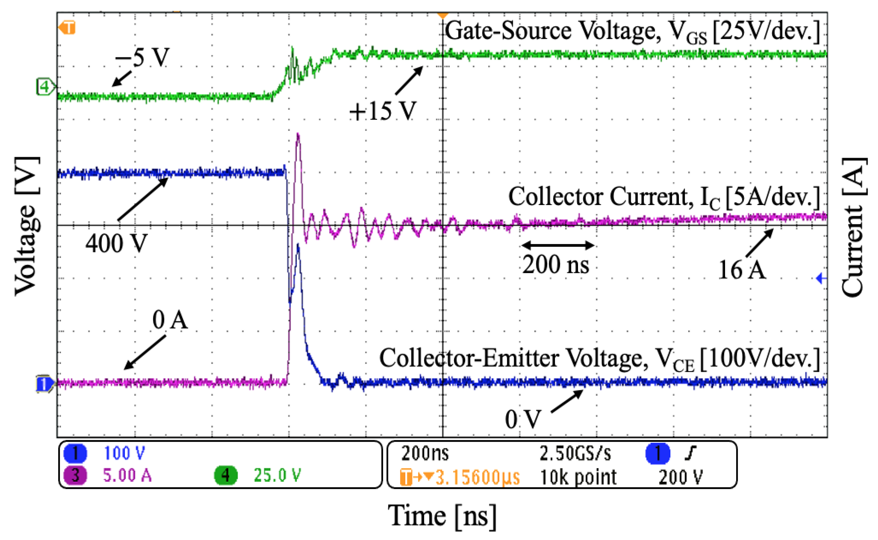
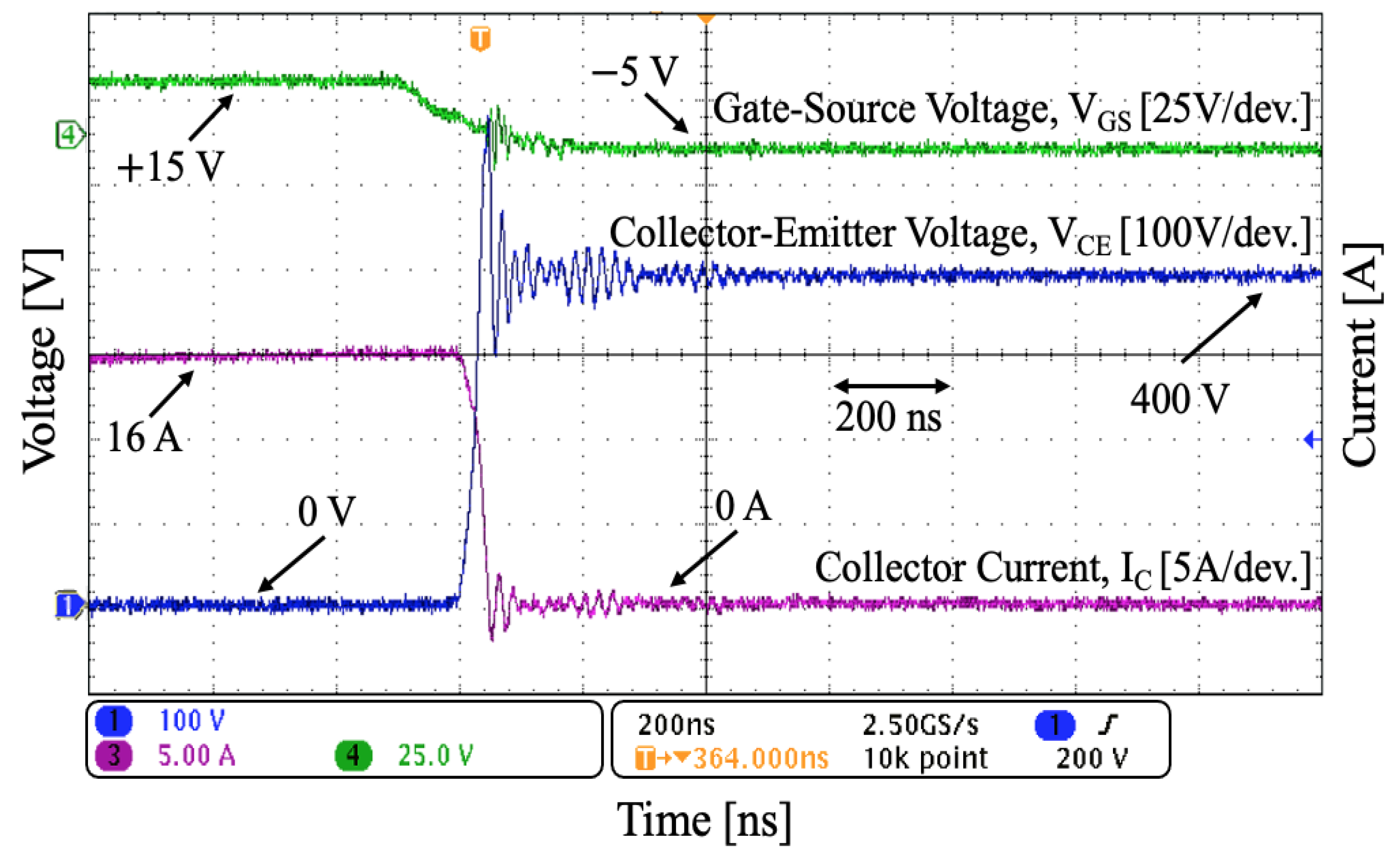
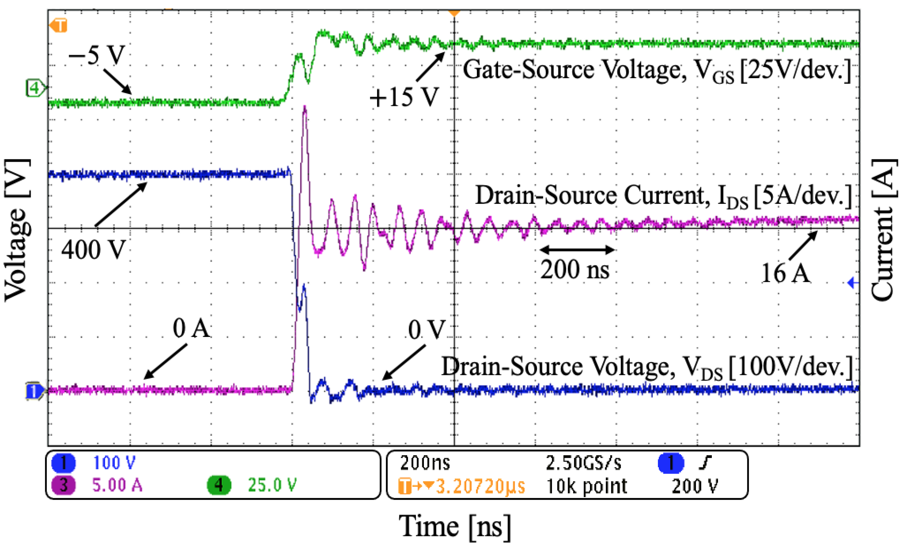
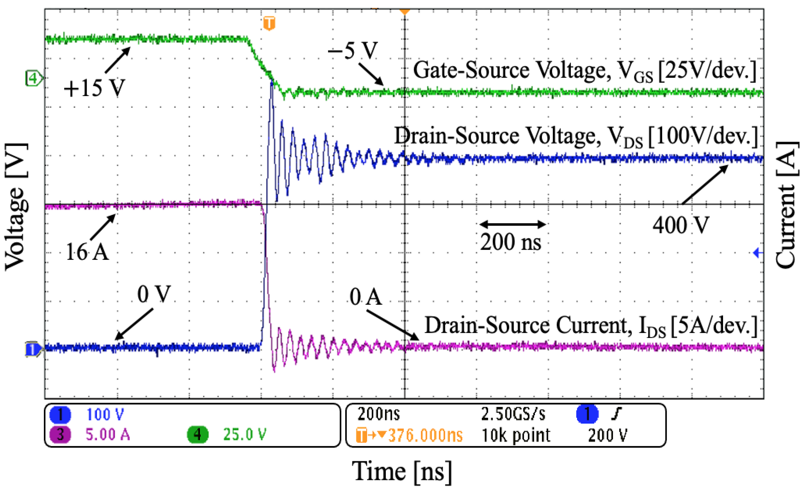
5.1. 900 V Si-IGBT Switching Performance

To analyze the characteristics of the Si-IGBT, the device is tested under the operating condition of a DC-link voltage of 400 V and switch current of 16 A. Figure 6 and Figure 7 depict the switching behavior of Si-IGBT at turn-on and turn-off durations. Gate driver voltages are considered to be +15/−5 V while the turning-on and turning-off gate resistances are 5 Ω and 20 Ω , respectively. As the device is turned on and turned off, the measurements of the switching energies are 445 μ J and 205 μ J, respectively. The Si-IGBT exhibits higher switching energy losses with a current overshoot of 29 A in the switching-on. At the turn-off, the Si device has a voltage overshoot of 580 V because of the parasitic parameters of the current commutating.

5.2. 900 V SiC-MOSFET Switching Performance

To demonstrate the SiC-MOSFET characteristics, the switch device is examined under the operating condition of a DC-link voltage of 400 V and switch current of 16 A, as shown in Figure 8 and Figure 9. For switching on and off at identical operating conditions, a positive and negative gate voltage of +15 V and −5 V are applied to the SiC-MOSFET with gate resistances of 5 Ω and 20 Ω , respectively. The measured switching energies are 223 μ J and 35 μ J as the device is turned on and turned off. It can be observed that SiC-MOSFET exhibits a distinct oscillation in the switching waveforms because of the power loop inductance and stray capacitance of the board circuit. However, the SiC-MOSFET has much lower switching losses than that of the Si-IGBT during the switching-on and off conditions. The total energy loss is decreased by up to three times with SiC-MOSFET.

5.3. Switching Energy Losses

The energy losses are calculated from the device voltage and current waveforms during the turn-on and turn-off events, while the total energy loss ( E t o t a l ) is the summation of the turn-on and turn-off energy losses under varying input voltage values at room temperature. The two different semiconductor power devices are tested through the DPT circuit and evaluated at various switch currents, gate resistances, and input voltages.

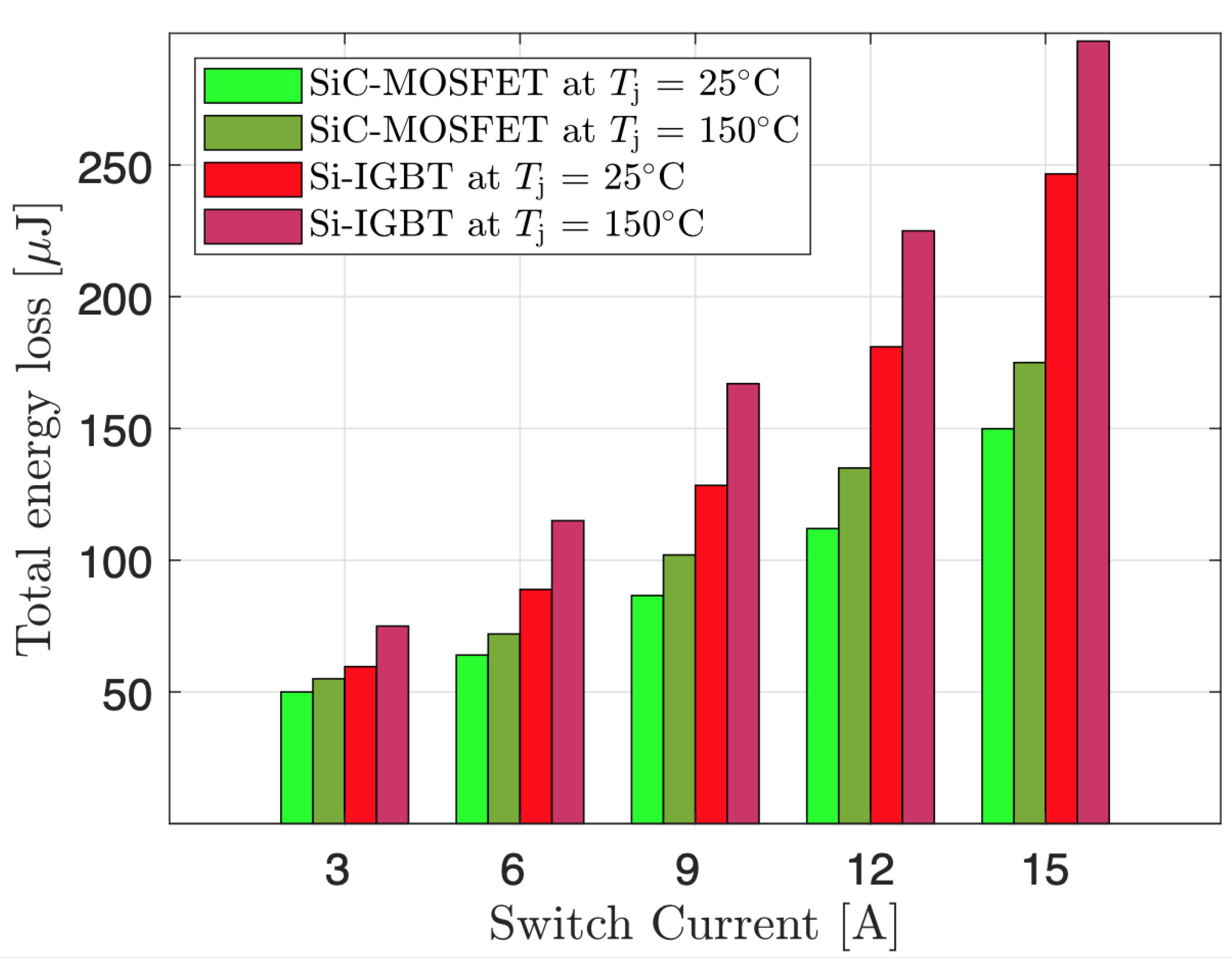
5.3.1. Switching Losses with Different Switch Currents

To assess each device’s performance, the energy loss during the turn-on and turn-off transitions is examined under various switch currents. During the examination, the DC-link voltage is typically kept constant at 400 V, allowing the effect of changing current on switching energy loss to be isolated and consistent testing operation conditions obtained. The current level in the DPT circuit is increased by adjusting the duration of the first pulse and the inductor value. The energy switching loss for each power device is measured as the switch current rises from 3 A to 15 A. Although the energy losses for both power devices increase almost linearly, the Si-IGBT suffers from a large loss during the switching-on and off periods, resulting in poor operating behavior when increasing the current. The use of SiC-MOSFET shows a significant reduction in energy losses at higher current levels due to the higher bandgap energy and lower capacitance compared to Si devices. The SiC power device experiences lower energy loss with the current elevation during the switching transitions, as illustrated in Table 3. It is noted that the SiC device achieved a reduction of nearly 40% in the overall energy losses at the highest current condition. Thus, SiC-MOSFET demonstrates excellent performance and exhibits lower energy losses under elevated current levels.
In addition, the switching loss of the two devices is tested at normal and high operating temperatures. To evaluate the effect of rising temperature on the device’s performance, a hotplate (MS300) is utilized to increase the operating temperature of the examined device through a heat sink. This approach can effectively test the selected device while ensuring safe examination. Figure 10 highlights that SiC-MOSFET maintains a lower total energy loss even at higher currents and temperatures because the SiC material exhibits excellent thermal conductivity and stellar melting points. It is observed that Si-IGBT is unable to effectively handle higher operating temperatures as it shows considerable total energy loss. The substantial decrease in the switching energy loss of the power devices is very important for estimating the overall efficiency of power electronic converters and the maximum junction temperature of each device technology. Efficiency improvements in the power converters can be enhanced by incorporating SiC power devices, which can compensate for the switching energy losses working at higher switching frequency operation, thereby allowing the use of smaller reactive components and cooling systems.

5.3.2. Energy Losses with Different Gate Resistances

The gate resistance value ( R G ) has a major impact on the energy losses, current and voltage oscillations, and switching periods. In the DPT circuit, the DC-link voltage is set up to 400 V and the switch current is performed at 10 A to record the energy loss of each tested device as the gate resistance is changed incrementally from 5 Ω to 25 Ω . Table 4 shows the measured total energy loss at two different operating conditions as the gate resistance is increased. It is noted that the total energy loss of the SiC-MOSFET increases slightly while the total energy loss of the Si-IGBT increases significantly with increase in the gate resistance. The SiC-MOSFET achieves a 45% decrease in overall energy loss compared to the total energy loss for the Si-IGBT. By testing the gate resistance effect, higher R G causes the device to switch more slowly, leading to higher energy loss due to the longer switching times. However, the higher values of gate resistance can clearly reduce the overshoot in the current and voltage waveforms due to lower d v / d t and d i / d t rates. In other words, lower R G causes the device to switch faster, resulting in lower energy loss because of the shorter switching times. The drawback of smaller gate resistance is increasing the ringing in the device waveforms because of higher d v / d t and d i / d t rates. This gives rise to a higher risk of device stress and failure. Therefore, it is important to obtain the optimal value of R G that can balance the low energy loss and reasonable overshoot. Under the test investigation, the gate resistance of 15 Ω exhibits better performance for examined devices showing manageable switching losses and oscillations.

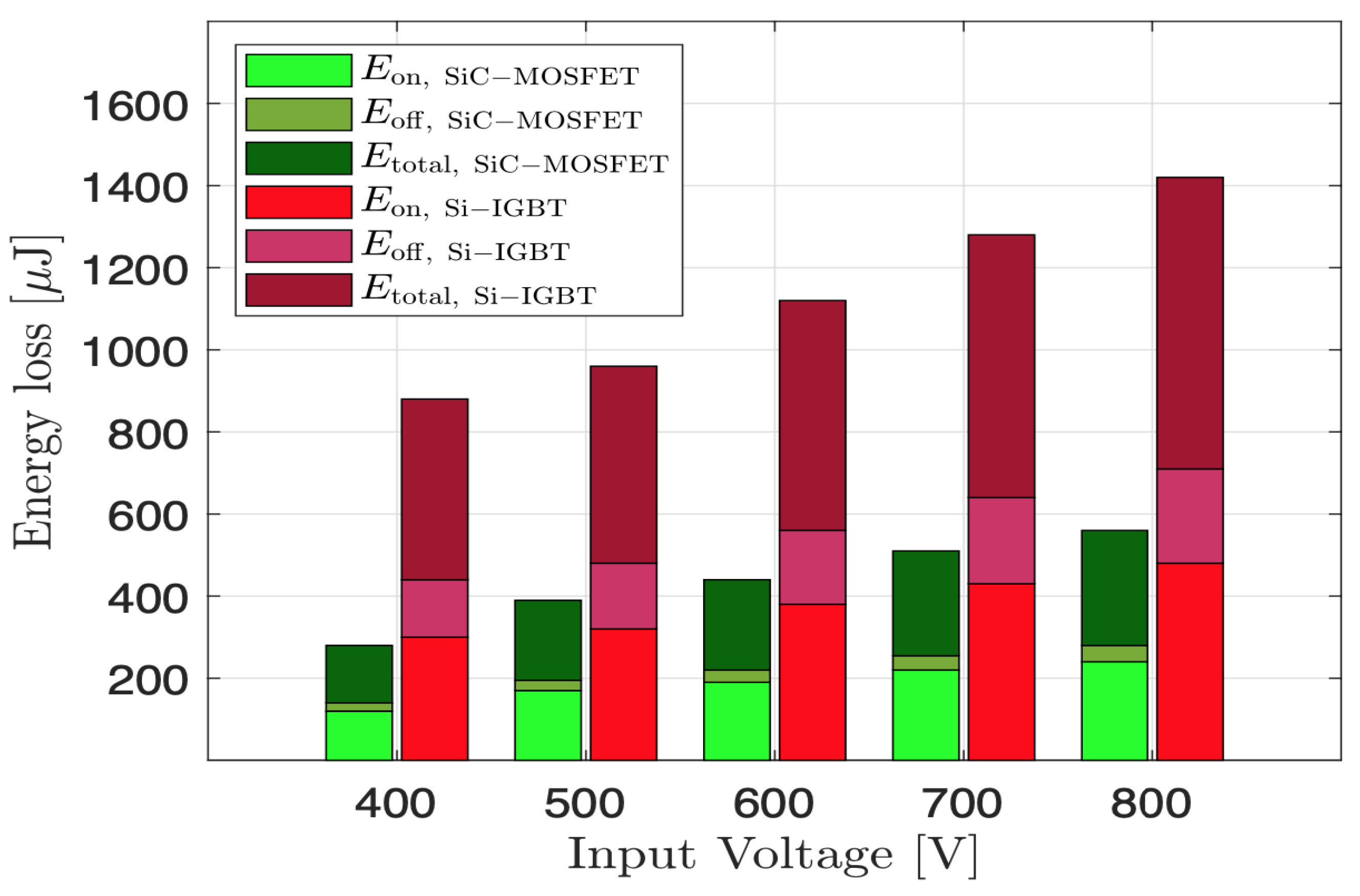
5.3.3. Switching Losses with Different Input Voltages

In the DPT circuit, the effect of the input voltage (i.e., DC bus voltage, V d c ) is tested to analyze the device stress as well as the variations in the voltage influence in terms of energy losses. To set up the test, the DC power supply is used to provide a variable voltage (from 400 V to 800 V), considering the rated voltage of the examined device. In the meantime, the inductor current remains fixed at 10 A for each input voltage by modifying the first pulse duration. Figure 11 shows all the energy losses are expected to increase with a higher voltage as the switching losses are proportional to the device voltage and current waveforms. It is noted that the turn-on loss of the SiC-MOSFET increases as the voltage level changes from 400 V to 800 V. At the same time, the turn-off loss of this device remains negligible and almost unchanged as the voltage level increases. In the Si-IGBT, both the turn-on and turn-off energy losses increase drastically because this device exhibits higher rise voltage during the turning-on event and larger tail current during the turning-off event. Additionally, Si-IGBT had a large value of input and output capacitances, causing major capacitive losses. At the input voltage of 800 V, the total energy loss is 282.5 μ J for the SiC-MOSFET and 711.8 μ J for the Si-IGBT. It is demonstrated that the SiC power device has substantial decreases in the total energy dissipation over a wide voltage range. Therefore, the SiC device possesses lower energy losses with the changes in switch currents, gate resistances, and input voltages compared with the Si device. Using SiC devices can allow power converter design to achieve superior switching performance with a notable improvement in efficiency at higher switching frequencies and load conditions.

6. Inverter Performance Evaluation

Several previous articles and works have focused on the application of SiC semiconductor power devices rated at 1200 V or higher in renewable energy systems [78,79,80]. Their outcomes highlight a significant reduction in semiconductor losses and improved efficiency with the incorporation of SiC power devices compared to Si-based inverters. However, these studies have not fully investigated the application of the low-medium voltage level of 900 V SiC power devices at both the device and inverter level and comparing them to Si-based inverters. There is an important need to meet the requirements of emerging applications, such as solar inverters, which typically operate at voltage levels below 950 V. In this section, the switching performance and energy efficiency of emerging 900 V SiC power devices are explored, with a focus on their integration into VSI inverter systems for PV applications.
The inverter performance comparison of different power devices is presented under various switching frequencies and input voltage conditions. In this study, a three-phase PV inverter was chosen for comparison evaluation, whose simulation mode is illustrated in Figure 12. The inverter specifications are given in Table 5. Figure 13 illustrates the results of the simulated three-phase inverter, including the switching signal, the DC-Link voltage, and the grid current. The inverter with each power device technology is performed and simulated in PLECS version 4.8.10 using the probe loss model of the devices according to the switching device’s data. At the input and output sides of the inverter, the voltage and current are computed under each test condition to calculate the loss dissipation and energy efficiency.

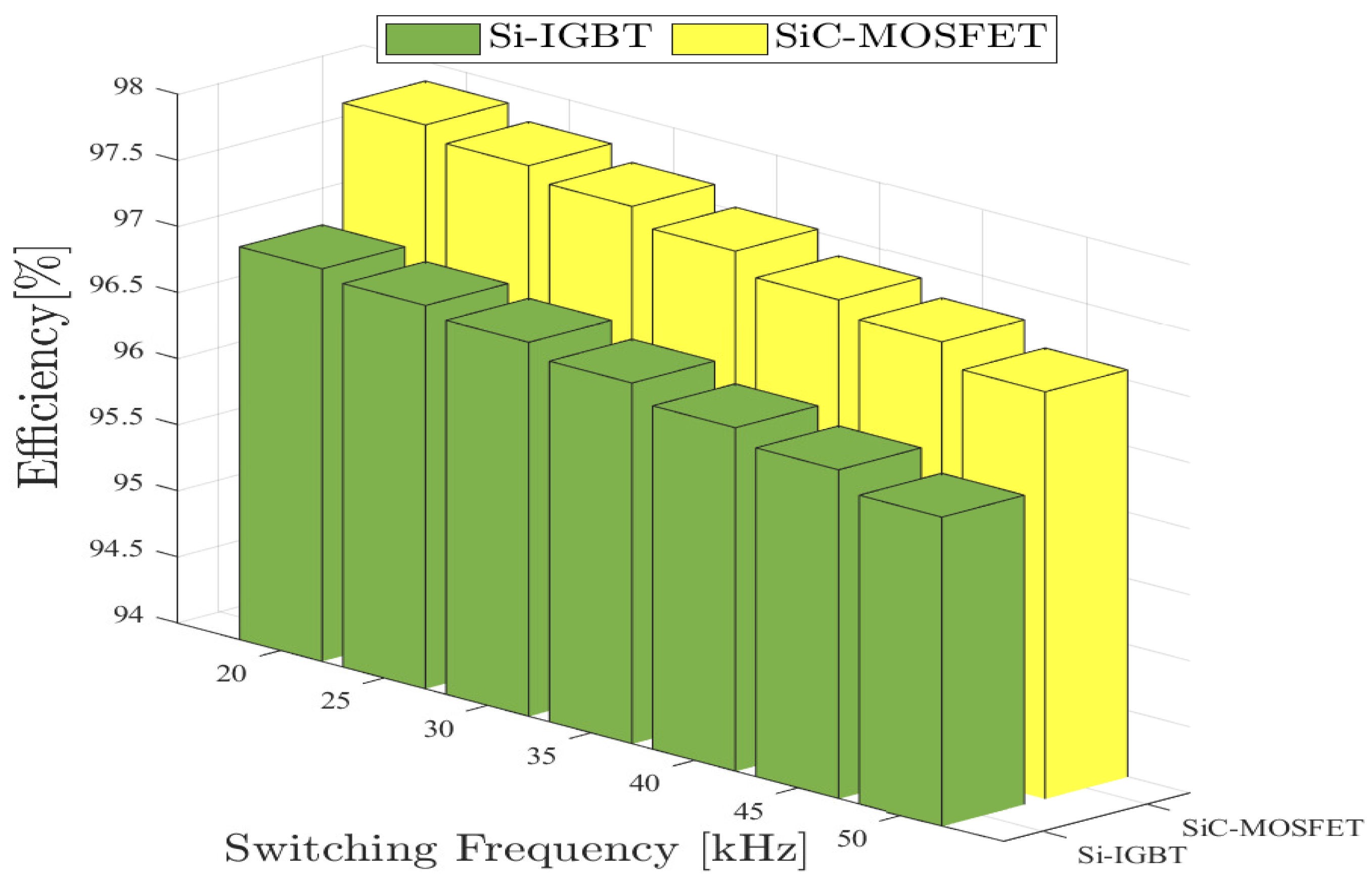
6.1. Inverter Evaluation as Increasing Switching Frequency

The inverter efficiency with each power device under various switching frequencies is presented in Figure 14. The inverter with SiC-MOSFET provides lower total loss and shows efficiency improvement under high switching frequency conditions. The inverter is substantially decreased by employing SiC-MOSFETs because of their outstanding characteristics and performance in comparison with the conventional Si-based inverter. It is observed that the inverter efficiency with SiC-MOSFET remains above 97% within the tested frequency range. The inverter with SiC power devices exhibits higher efficiency in comparison with the conventional inverter due to lower device losses and enhanced switching performance. Therefore, the inverter with SiC power devices can deliver superior overall efficiency while minimizing the size and weight of the reactive components under harsh operating conditions because of the superiority of SiC semiconductor devices.

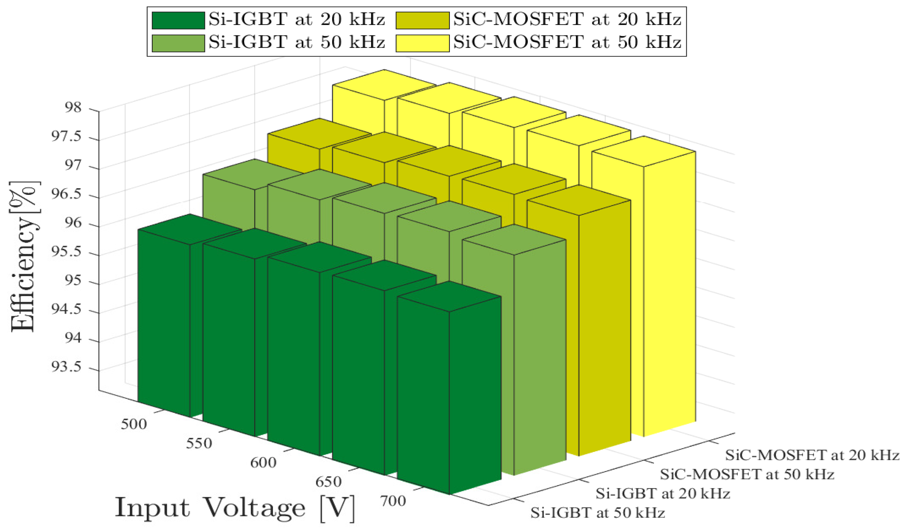
6.2. Inverter Evaluation as Increasing Input Voltage

The input voltage is raised from 550 V to 700 V to test the inverter performance under two different switching frequency conditions. Figure 15 illustrates the improvement in the inverter efficiency by using SiC-MOSFET. The SiC-based inverter shows efficient and better performance across a wide range of input voltages, resulting in a significant improvement in the overall efficiency. The inverter with Si-IGBT can achieve only 96.34% at 700 V of the input voltage and 50 kHz of the switching frequency, whereas the inverter with SiC-MOSFET devices has an efficiency of 97.36% and its efficiency shows a marginal decrease of less than 1% in the overall efficiency with the input voltage elevation. The inverter with SiC-MOSFETs has the highest efficiency performance at the higher switching frequency and input voltage. The results demonstrate that SiC-MOSFETs have efficient conduction and switching performance across various operating conditions, which allows PV inverters to sustain a high efficiency level while functioning at high load and switching conditions.

7. Conclusions

The device performance and energy loss comparisons of the selected device technologies are presented and discussed at various gate resistances, current, and voltage conditions. SiC-MOSFETs exhibit significantly lower switching losses, which dominate the total power loss of the inverter design. This will enhance the switching performance and improve energy conversion for hard-switching applications. The results illustrate that the total switching energy losses are decreased by nearly 50% and the inverter’s overall efficiency is improved from 96.34% to 97.85% by using SiC-MOSFETs power devices under high operating conditions. The SiC-based inverter shows robust performance, and its efficiency remains above 97% at different values of input voltage and switching frequency. These findings show the advantages of using SiC devices in three-phase inverters operating under harsh environmental conditions, enabling substantial decreases in the weight and size of reactive components without compromising inverter efficiency.

Author Contributions

Conceptualization, S.S.A. (Saleh S. Alharbi) and S.S.A. (Salah S. Alharbi); methodology, S.S.A. (Saleh S. Alharbi) and S.S.A. (Salah S. Alharbi); software, S.S.A. (Saleh S. Alharbi), S.S.A. (Salah S. Alharbi) and A.B.; validation, S.S.A. (Saleh S. Alharbi), S.S.A. (Salah S. Alharbi), A.B., H.A. and A.A.; formal analysis, S.S.A. (Salah S. Alharbi), A.A. and H.A.; investigation, S.S.A. (Saleh S. Alharbi), A.A. and A.B.; resources, S.S.A. (Saleh S. Alharbi) and S.S.A. (Salah S. Alharbi); data curation, S.S.A. (Saleh S. Alharbi) and S.S.A. (Salah S. Alharbi); writing—original draft preparation, S.S.A. (Saleh S. Alharbi) and H.A.; writing—review and editing, S.S.A. (Salah S. Alharbi), A.B. and A.A.; visualization, A.B., H.A. and A.A.; supervision, H.A. and A.A.; project administration, S.S.A. (Saleh S. Alharbi); funding acquisition, S.S.A. (Saleh S. Alharbi) and S.S.A. (Salah S. Alharbi). All authors have read and agreed to the published version of the manuscript.

Funding

This research was funded by the Deanship of Innovation and Scientific Research, contract no. (1442/17), at Al-Baha University, Alaqiq, Saudi Arabia.

Institutional Review Board Statement

Not applicable.

Informed Consent Statement

Not applicable.

Data Availability Statement

The data are available on request from the corresponding auther.

Conflicts of Interest

The authors declare no conflicts of interest.

References

  1. Alluhaybi, K.; Batarseh, I.; Hu, H. Comprehensive Review and Comparison of Single-Phase Grid-Tied Photovoltaic Microinverters. IEEE J. Emerg. Sel. Top. Power Electron. 2020, 8, 1310–1329. [Google Scholar] [CrossRef]
  2. Kjaer, S.B.; Pedersen, J.K.; Blaabjerg, F. A review of single-phase grid-connected inverters for photovoltaic modules. IEEE Trans. Ind. Appl. 2005, 41, 1292–1306. [Google Scholar] [CrossRef]
  3. International Energy Agency (IEA). Tracking SDG7: The Energy Progress Report. 2021. Available online: https://www.iea.org/reports/tracking-sdg7-the-energy-progress-report-2021 (accessed on 8 October 2024).
  4. SolarPower Europe. Global Market Outlook for Solar Power 2024–2028. 2024. Available online: https://www.solarpowereurope.org/insights/outlooks/global-market-outlook-for-solar-power-2024-2028 (accessed on 9 October 2024).
  5. Haque, M.M.; Wolfs, P.J.; Alahakoon, S.; Islam, M.A.; Nadarajah, M.; Zare, F.; Farrok, O. Three-Port Converters for Energy Conversion of PV-BES Integrated Systems—A Review. IEEE Access 2023, 11, 6551–6573. [Google Scholar] [CrossRef]
  6. Bhattacharjee, A.K.; Kutkut, N.; Batarseh, I. Review of Multiport Converters for Solar and Energy Storage Integration. IEEE Trans. Power Electron. 2019, 34, 1431–1445. [Google Scholar] [CrossRef]
  7. Abdel-Rahim, O.; Chub, A.; Vinnikov, D.; Blinov, A. DC Integration of Residential Photovoltaic Systems: A Survey. IEEE Access 2022, 10, 66974–66991. [Google Scholar] [CrossRef]
  8. Xue, Y.; Chang, L.; Kjaer, S.B.; Bordonau, J.; Shimizu, T. Topologies of single-phase inverters for small distributed power generators: An overview. IEEE Trans. Power Electron. 2004, 19, 1305–1314. [Google Scholar] [CrossRef]
  9. Tang, Z.; Yang, Y.; Blaabjerg, F. Power electronics: The enabling technology for renewable energy integration. CSEE J. Power Energy Syst. 2022, 8, 39–52. [Google Scholar] [CrossRef]
  10. Maurya, J.; Saket, R.K.; Srivastava, R.K. Performance Analysis of Single-Stage and Two-Stage VSI-Fed Induction Motor Drives for Solar Water Pumping Applications. IEEE Trans. Ind. Appl. 2024, 60, 8856–8866. [Google Scholar] [CrossRef]
  11. Pal, A.; Basu, K. A Soft-Switched High-Frequency Link Single-Stage Three-Phase Inverter for Grid Integration of Utility Scale Renewables. IEEE Trans. Power Electron. 2019, 34, 8513–8527. [Google Scholar] [CrossRef]
  12. Bairami, S.; Salimi, M.; Mirabbasi, D. A Novel Method for Maximum Power Point Tracking of the Grid-Connected Three-Phase Solar Systems Based on the PV Current Prediction. Chin. J. Electron. 2023, 32, 353–364. [Google Scholar] [CrossRef]
  13. Ibrahim, N.F.; Mahmoud, K.; Lehtonen, M.; Darwish, M.M.F. Comparative Analysis of Three-Phase PV Grid Connected Inverter Current Control Schemes in Unbalanced Grid Conditions. IEEE Access 2023, 11, 42204–42221. [Google Scholar] [CrossRef]
  14. Kim, M.; Yun, H.-J. A Basic Design Tool for Grid-Connected AC–DC Converters Using Silcon Carbide MOSFETs. Electronics 2023, 12, 4828. [Google Scholar] [CrossRef]
  15. Sajadian, S.; Ahmadi, R. Model Predictive-Based Maximum Power Point Tracking for Grid-Tied Photovoltaic Applications Using a Z-Source Inverter. IEEE Trans. Power Electron. 2016, 31, 7611–7620. [Google Scholar] [CrossRef]
  16. Yazdani, S.; Ferdowsi, M.; Davari, M.; Shamsi, P. Advanced Current-Limiting and Power-Sharing Control in a PV-Based Grid-Forming Inverter Under Unbalanced Grid Conditions. IEEE J. Emerg. Sel. Top. Power Electron. 2020, 8, 1084–1096. [Google Scholar] [CrossRef]
  17. Costa, P.; Pinto, S.; Silva, J.F. A Novel Analytical Formulation of SiC-MOSFET Losses to Size High-Efficiency Three-Phase Inverters. Energies 2023, 16, 818. [Google Scholar] [CrossRef]
  18. Rujas, A.; Landaburu, I.; Lopez-Martin, V.M.; Barambones, O. Magnetic Design of a 3-Phase SiC-Based PV Inverter with DC-Link Referenced Output Filter. IEEE Access 2023, 11, 25531–25542. [Google Scholar] [CrossRef]
  19. Stepenko, S.; Husev, O.; Vinnikov, D.; Roncero-Clemente, C.; Pires Pimentel, S.; Santasheva, E. Experimental Comparison of Two-Level Full-SiC and Three-Level Si–SiC Quasi-Z-Source Inverters for PV Applications. Energies 2019, 12, 2509. [Google Scholar] [CrossRef]
  20. Marzoughi, A.; Burgos, R.; Boroyevich, D. Characterization and Performance Evaluation of the State-of-the-Art 3.3 kV 30 A Full-SiC MOSFETs. IEEE Trans. Ind. Appl. 2019, 55, 575–583. [Google Scholar] [CrossRef]
  21. Fuentes, C.D.; Müller, M.; Bernet, S.; Kouro, S. SiC-MOSFET or Si-IGBT: Comparison of Design and Key Characteristics of a 690 V Grid-Tied Industrial Two-Level Voltage Source Converter. Energies 2021, 14, 3054. [Google Scholar] [CrossRef]
  22. Wang, Y.; Chen, M.; Xu, D. Design of Low Inductance SiC MOS/Si-IGBT Hybrid Module for PV Inverters. IEEE Open J. Power Electron. 2022, 3, 942–954. [Google Scholar] [CrossRef]
  23. Chakraborty, R.; Eskilson, T.; Biswas, S.; Makoschitz, M. A Comparative Analysis of Efficiency and Losses in a 5 kW Hybrid and Full-SiC Converter, for PV Applications in Austria. Energies 2024, 17, 5600. [Google Scholar] [CrossRef]
  24. Khodabandeh, M.; Afshari, E.; Amirabadi, M. A Single-Stage Soft-Switching High-Frequency AC-Link PV Inverter: Design, Analysis, and Evaluation of Si-Based and SiC-Based Prototypes. IEEE Trans. Power Electron. 2019, 34, 2312–2326. [Google Scholar] [CrossRef]
  25. Loncarski, J.; Monopoli, V.G.; Leuzzi, R.; Ristic, L.; Cupertino, F. Analytical and Simulation Fair Comparison of Three Level Si IGBT Based NPC Topologies and Two Level SiC MOSFET Based Topology for High Speed Drives. Energies 2019, 12, 4571. [Google Scholar] [CrossRef]
  26. Woldegiorgis, D.; Mantooth, H.A. Precise Electro-thermal Power Loss Model of a Three-level ANPC Inverter with Hybrid Si/SiC Switches. Chin. J. Electr. Eng. 2022, 8, 76–89. [Google Scholar] [CrossRef]
  27. Liu, H.; Zhao, T.; Wu, X. Performance Evaluation of Si/SiC Hybrid Switch-Based Three-Level Active Neutral-Point-Clamped Inverter. IEEE Open J. Ind. Appl. 2022, 3, 90–103. [Google Scholar] [CrossRef]
  28. Wang, K.; Ma, D.; Hu, B.; Wang, J.; Singh, A.; Mather, B. Hardware Design of Medium Voltage SiC-based Modular Multilevel Converters for Grid-tied Applications. In Proceedings of the 2021 IEEE 8th Workshop on Wide Bandgap Power Devices and Applications (WiPDA), Redondo Beach, CA, USA, 7–11 November 2021; pp. 339–344. [Google Scholar] [CrossRef]
  29. Haghighian, S.K.; Yeh, H.G.; Marangalu, M.G.; Kurdkandi, N.V.; Abbasi, M.; Tarzamni, H. A Seventeen-Level Step-Up Switched-Capacitor-Based Multilevel Inverter with Reduced Charging Current Stress on Capacitors for PV Applications. IEEE Access 2023, 11, 118124–118143. [Google Scholar] [CrossRef]
  30. Kala, P.; Jately, V.; Sharma, A.; Joshi, J.; Azzopardi, B. ASO-Based SHE Method on Hybrid Multilevel Inverter for PV Application Under Dynamic Operating Conditions. IEEE Access 2023, 11, 98093–98114. [Google Scholar] [CrossRef]
  31. Marques, G.D.; Cruz, S.M.A.; Iacchetti, M.F. Minimum-Loss Control Strategy for a Dual-VSI DFIG DC System. IEEE Trans. Ind. Electron. 2020, 67, 8175–8185. [Google Scholar] [CrossRef]
  32. Wang, Y.; Li, H.; Liu, R.; Yang, L.; Wang, X. Modulated Model-Free Predictive Control with Minimum Switching Losses for PMSM Drive System. IEEE Access 2020, 8, 20942–20953. [Google Scholar] [CrossRef]
  33. Kumar, A.; Moradpour, M.; Losito, M.; Franke, W.-T.; Ramasamy, S.; Baccoli, R.; Gatto, G. Wide Band Gap Devices and Their Application in Power Electronics. Energies 2022, 15, 9172. [Google Scholar] [CrossRef]
  34. Chaudhary, O.S.; Denaï, M.; Refaat, S.S.; Pissanidis, G. Technology and Applications of Wide Bandgap Semiconductor Materials: Current State and Future Trends. Energies 2023, 16, 6689. [Google Scholar] [CrossRef]
  35. Buffolo, M.; Favero, D.; Marcuzzi, A.; Santi, C.D.; Meneghesso, G.; Zanoni, E.; Meneghini, M. Review and Outlook on GaN and SiC Power Devices: Industrial State-of-the-Art, Applications, and Perspectives. IEEE Trans. Electron. Devices 2024, 71, 1344–1355. [Google Scholar] [CrossRef]
  36. Ballestín-Fuertes, J.; Muñoz-Cruzado-Alba, J.; Sanz-Osorio, J.F.; Laporta-Puyal, E. Role of Wide Bandgap Materials in Power Electronics for Smart Grids Applications. Electronics 2021, 10, 677. [Google Scholar] [CrossRef]
  37. Zhang, B.; Wang, S. A Survey of EMI Research in Power Electronics Systems With Wide-Bandgap Semiconductor Devices. IEEE J. Emerg. Sel. Top. Power Electron. 2020, 8, 626–643. [Google Scholar] [CrossRef]
  38. DiMarino, C.M.; Burgos, R.; Dushan, B. High-temperature silicon carbide:characterization of state-of-the-art silicon carbide power transistors. IEEE Ind. Electron. Mag. 2015, 9, 19–30. [Google Scholar] [CrossRef]
  39. Alharbi, S.S.; Matin, M. Experimental evaluation of medium-voltage cascode gallium nitride (GaN) devices for bidirectional DC-DC converters. CES Trans. Elect. Mach. Syst. 2021, 5, 232–248. [Google Scholar] [CrossRef]
  40. Iannaccone, G.; Sbrana, C.; Morelli, I.; Strangio, S. Power Electronics Based on Wide-Bandgap Semiconductors: Opportunities and Challenges. IEEE Access 2021, 9, 139446–139456. [Google Scholar] [CrossRef]
  41. Bindra, A. Wide-Bandgap-Based Power Devices: Reshaping the power electronics landscape. IEEE Power Electron. Mag. 2015, 2, 42–47. [Google Scholar] [CrossRef]
  42. Wang, Y.; Ding, Y.; Yin, Y. Reliability of Wide Band Gap Power Electronic Semiconductor and Packaging: A Review. Energies 2022, 15, 6670. [Google Scholar] [CrossRef]
  43. Cunningham, D.W.; Carlson, E.P.; Manser, J.S.; Kizilyalli, I.C. Impacts of Wide Band Gap Power Electronics on Photovoltaic System Design. IEEE J. Photovoltaics 2020, 10, 213–218. [Google Scholar] [CrossRef]
  44. Shi, Y.; Li, H.; Wang, L.; Zhang, Y. Intercell Transformer (ICT) Design Optimization and Interphase Crosstalk Mitigation of a 100-kW SiC Filter-Less Grid-Connected PV String Inverter. IEEE Open J. Power Electron. 2020, 10, 51–63. [Google Scholar] [CrossRef]
  45. Narasimhan, S.; Kanale, A.; Bhattacharya, S.; Baliga, J.B. Performance Evaluation of 3.3 kV SiC MOSFET and Schottky Diode Based Reverse Voltage Blocking Switch for Medium Voltage Current Source Inverter Application. IEEE Access 2020, 10, 89277–89289. [Google Scholar] [CrossRef]
  46. Acharya, S.; She, X.; Tao, F.; Frangieh, T.; Todorovic, M.H.; Datta, R. Active Gate Driver for SiC-MOSFET-Based PV Inverter With Enhanced Operating Range. IEEE Trans. Ind. Appl. 2010, 55, 1677–1689. [Google Scholar] [CrossRef]
  47. Yin, T.; Xu, C.; Lin, L.; Jing, K. A SiC MOSFET and Si IGBT Hybrid Modular Multilevel Converter with Specialized Modulation Scheme. IEEE Trans. Power Electron. 2020, 35, 12623–12628. [Google Scholar] [CrossRef]
  48. Kang, Z.; Xie, X.; Liu, Y.; Chen, D.; Yuan, H.; Zhao, L.; Zhao, H.; Yang, C.; Zheng, G. A High-Voltage Pulse Modulator Composed of SiC MOSFETs/IGBTs in a Hybrid Connecting State. Electronics 2024, 13, 2108. [Google Scholar] [CrossRef]
  49. Huang, J.; Wang, Y.; Li, Z.; Zhu, H.; Li, K. A Si IGBT/SiC MOSFET Hybrid Isolated Bidirectional DC–DC Converter for Reducing Losses and Costs of DC Solid State Transformer. Electronics 2024, 13, 801. [Google Scholar] [CrossRef]
  50. Hazra, S.; De, A.; Cheng, L.; Palmour, J.; Schupbach, M.; Hull, B.A.; Allen, S.; Bhattacharya, S. High Switching Performance of 1700-V, 50-A SiC Power MOSFET Over Si IGBT/BiMOSFET for Advanced Power Conversion Applications. IEEE Trans. Power Electron. 2016, 31, 4742–4754. [Google Scholar] [CrossRef]
  51. Yin, S.; Wu, Y.; Liu, Y.; Pan, X. Comparative Design of Gate Drivers with Short-Circuit Protection Scheme for SiC MOSFET and Si IGBT. Energies 2019, 12, 4546. [Google Scholar] [CrossRef]
  52. Sheikhan, A.; Narayanan, E.M.S. Characteristics of a 1200 V Hybrid Power Switch Comprising a Si IGBT and a SiC MOSFET. Micromachines 2024, 15, 1337. [Google Scholar] [CrossRef]
  53. Yin, T.; Lin, L.; Xu, C.; Zhu, D.; Jing, K. A Hybrid Modular Multilevel Converter Comprising SiC MOSFET and SiIGBT with Its Specialized Modulation and Voltage Balancing Scheme. IEEE Trans. Ind. Electron. 2022, 11, 11272–11282. [Google Scholar] [CrossRef]
  54. Zhou, W.; Yuan, X. Experimental Evaluation of SiC Mosfets in Comparison to Si IGBTs in a Soft-Switching Converter. IEEE Trans. Ind. Appl. 2020, 56, 5108–5118. [Google Scholar] [CrossRef]
  55. Vechalapu, K.; Bhattacharya, S.; Brunt, E.V.; Ryu, S.H.; Grider, D.; Palmour, J.W. Comparative Evaluation of 15-kV SiC MOSFET and 15-kV SiC IGBT for Medium-Voltage Converter Under the Same dv/dt Conditions. IEEE J. Emerg. Sel. Top. Power Electron. 2017, 5, 469–489. [Google Scholar] [CrossRef]
  56. Burkart, R.M.; Kolar, J.W. Comparative Life Cycle Cost Analysis of Si and SiC PV Converter Systems Based on Advanced η- ρ-σ Multiobjective Optimization Techniques. IEEE Trans. Power Electron. 2017, 32, 4344–4358. [Google Scholar] [CrossRef]
  57. Chen, H.J.; Kusic, G.L.; Reed, G.F. Comparative PSCAD and Matlab/Simulink simulation models of power losses for SiC MOSFET and Si IGBT devices. In Proceedings of the 2012 IEEE Power and Energy Conference at Illinois, Champaign, IL, USA, 24–25 February 2012; pp. 1–5. [Google Scholar] [CrossRef]
  58. Öztürk, S.; Canver, M.; Çadırcı, I.; Ermiş, M. All SiC Grid-Connected PV Supply with HF Link MPPT Converter: System Design Methodology and Development of a 20 kHz, 25 kVA Prototype. Electronics 2018, 7, 85. [Google Scholar] [CrossRef]
  59. Ning, P.; Yuan, T.; Kang, Y.; Han, C.; Li, L. Review of Si IGBT and SiC MOSFET based on hybrid switch. Chin. J. Electr. Eng. 2019, 5, 20–29. [Google Scholar] [CrossRef]
  60. Xu, C.; He, J.; Lin, L. Research on Capacitor-Switching Semi-Full-Bridge Submodule of Modular Multilevel Converter Using Si IGBT and SiC MOSFET. IEEE J. Emerg. Sel. Top. Power Electron. 2021, 9, 4814–4825. [Google Scholar] [CrossRef]
  61. Hazra, S.; Madhusoodhanan, S.; Moghaddam, G.K.; Hatua, K.; Bhattacharya, S. Design Considerations and Performance Evaluation of 1200-V 100-A SiC MOSFET-Based Two-Level Voltage Source Converter. IEEE Trans. Ind. Appl. 2016, 52, 4257–4268. [Google Scholar] [CrossRef]
  62. Mirzaee, H.; De, A.; Tripathi, A.; Bhattacharya, S. Design Comparison of High-Power Medium-Voltage Converters Based on a 6.5-kV Si IGBT/Si-PiN Diode, a 6.5-kV Si IGBT/SiC-JBS Diode, and a 10-kV SiC MOSFET/SiC-JBS Diode. IEEE Trans. Ind. Appl. 2014, 50, 2728–2740. [Google Scholar] [CrossRef]
  63. Qi, J.; Yang, X.; Li, X.; Tian, K.; Mao, Z.; Yang, S.; Song, W. Temperature Dependence of Dynamic Performance Characterization of 1.2-kV SiCPower mosfets Compared With Si IGBTs for Wide Temperature Applications. IEEE Trans. Power Electron. 2019, 34, 9105–9117. [Google Scholar] [CrossRef]
  64. Fuentes, C.D.; Kouro, S.; Bernet, S. Comparison of 1700-V SiC-MOSFET and Si-IGBT Modules Under Identical Test Setup Conditions. IEEE Trans. Ind. Appl. 2019, 55, 7765–7775. [Google Scholar] [CrossRef]
  65. Shah, F.M.; Maqsood, S.; Damaševičius, R.; Blažauskas, T. Disturbance Rejection and Control Design of MVDC Converter with Evaluation of Power Loss and Efficiency Comparison of SiC and Si Based Power Devices. Electronics 2020, 9, 1878. [Google Scholar] [CrossRef]
  66. Jahan, S.; Biswas, S.P.; Haq, S.; Islam, M.R.; Mahmud, M.A.P.; Kouzani, A.Z. An advanced control scheme for voltage source inverter based grid-tied PV systems. IEEE Trans. Appl. Supercond. 2021, 31, 5401705. [Google Scholar] [CrossRef]
  67. Assunção, G.d.O.; Barbi, I. Method for deriving transformerless common-ground voltage source inverter topologies. IEEE Trans. Power Electron. 2022, 37, 10821–10832. [Google Scholar] [CrossRef]
  68. Hu, C.; Yin, Z.; Rui, T.; Zhang, Z.; Shen, W.; Cao, W.; Holmes, D.G. A novel double-voltage-vector model-free predictive current control method for two-level voltage source inverters. IEEE Trans. Ind. Electron. 2023, 70, 5872–5884. [Google Scholar] [CrossRef]
  69. Ahmed, M.H.; Wang, M.; Hassan, M.A.S.; Ullah, I. Power Loss Model and Efficiency Analysis of Three-Phase Inverter Based on SiC MOSFETs for PV Applications. IEEE Access 2019, 7, 75768–75781. [Google Scholar] [CrossRef]
  70. Safari, S.; Castellazzi, A.; Wheeler, P. Experimental and Analytical Performance Evaluation of SiC Power Devices in the Matrix Converter. IEEE Trans. Power Electron. 2014, 5, 2584–2596. [Google Scholar] [CrossRef]
  71. Ding, X.; Chen, F.; Du, M.; Guo, H.; Ren, S. Effects of silicon carbide MOSFETs on the efficiency and power quality of a microgrid-connected inverter. Appl. Energy 2017, 201, 270–283. [Google Scholar] [CrossRef]
  72. Gurpinar, E.; Castellazzi, A. Single-Phase T-Type Inverter Performance Benchmark Using Si IGBTs, SiC MOSFETs, and GaN HEMTs. IEEE Trans. Power Electron. 2016, 31, 7148–7160. [Google Scholar] [CrossRef]
  73. Amirpour, S.; Thiringer, T.; Hagstedt, D. Energy Loss Analysis in a SiC/IGBT Propulsion Inverter over Drive Cycles Considering Blanking time, MOSFET’s Reverse Conduction and the Effect of Thermal Feedback. In Proceedings of the 2020 IEEE Energy Conversion Congress and Exposition (ECCE), Detroit, MI, USA, 11–15 October 2020; pp. 1505–1511. [Google Scholar] [CrossRef]
  74. Dynex Semiconductor Ltd. AN6156–Calculating Power Losses in an IGBT Module. Available online: https://www.dynexsemi.com/Portals/0/assets/downloads/DNX_AN6156.pdf (accessed on 31 October 2024).
  75. Filipović-Grčić, D.; Filipović-Grčić, B.; Krajtner, D. Frequency response and harmonic distortion testing of inductive voltage transformer used for power quality measurements. In Proceedings of the 4th International Colloquium Transformer Research and Asset Management, Pula, Croatia, 10–12 May 2017; pp. 159–167. [Google Scholar] [CrossRef]
  76. Alharbi, S.S.; Alharbi, S.S.; Al-bayati, A.M.S.; Matin, M.A. Comparative performance evaluation of Si IGBT, SiC JFET, and SiC MOSFET power devices for a non-isolated DC-DC boost converter. In Proceedings of the 2017 North American Power Symposium (NAPS), Morgantown, WV, USA, 17–19 September 2017; pp. 1–6. [Google Scholar] [CrossRef]
  77. Havrlík, M.; Libra, M.; Poulek, V.; Kouřím, P. Analysis of Output Signal Distortion of Galvanic Isolation Circuits for Monitoring the Mains Voltage Waveform. Sensors 2022, 22, 7769. [Google Scholar] [CrossRef]
  78. Marzoughi, A.; Wang, J.; Burgos, R.; Boroyevich, D. Characterization and Evaluation of the State-of-the-Art 3.3-kV 400-A SiC MOSFETs. IEEE Trans. Ind. Electron. 2017, 64, 8247–8257. [Google Scholar] [CrossRef]
  79. Kranzer, D.; Wilhelm, C.; Reiners, F.; Burger, B. Application of normally-off SiC-JFETs in photovoltaic inverters. In Proceedings of the 2009 13th European Conference on Power Electronics and Applications, Barcelona, Spain, 8–10 September 2009; pp. 1–6. [Google Scholar]
  80. Villanueva, I.; Vázquez, N.; Vaquero, J.; Hernández, C.; López-Tapia, H.; Osorio-Sánchez, R. Photovoltaic Inverter Reliability Study through SiC Switches Redundant Structures. Technologies 2023, 11, 59. [Google Scholar] [CrossRef]
Figure 1. Off-grid and on-grid solar power systems.
Electronics 14 01061 g001
Figure 2. Schematic diagram of three-phase voltage source inverter used in the PV application.
Electronics 14 01061 g002
Figure 3. Ideal waveforms of the switching device.
Electronics 14 01061 g003
Figure 4. Circuit schematic of the DPT setup.
Electronics 14 01061 g004
Figure 5. DPT bench setup for switching characterization.
Electronics 14 01061 g005
Figure 6. Experimental turn-on switching waveform of Si-IGBT at a DC-link voltage of 400 V and switch current of 16 A.
Electronics 14 01061 g006
Figure 7. Experimental turn-off switching waveform of Si-IGBT at a DC-link voltage of 400 V and switch current of 16 A.
Electronics 14 01061 g007
Figure 8. Experimental turn-on switching waveform of SiC-MOSFET at a DC-link voltage of 400 V and switch current of 16 A.
Electronics 14 01061 g008
Figure 9. Experimental turn-off switching waveform of SiC-MOSFET at a DC-link voltage of 400 V and switch current of 16 A.
Electronics 14 01061 g009
Figure 10. Total switching energy losses for Si-IGBT and SiC-MOSFET under different switch currents and at junction temperatures of 25 °C and 150 °C.
Electronics 14 01061 g010
Figure 11. Turn-on, turn-off, and total switching energy losses for Si-IGBT and SiC-MOSFET at different input voltages.
Electronics 14 01061 g011
Figure 12. Simulated three-phase VSI connected to the grid.
Electronics 14 01061 g012
Figure 13. Three-phase inverter simulation results: (a) switching signal; (b) DC-Link voltage; (c) grid current.
Electronics 14 01061 g013
Figure 14. Efficiency of the inverter at different switching frequency values.
Electronics 14 01061 g014
Figure 15. Efficiency of the inverter at different input voltage values under two switching frequencies of 20 kHz and 50 kHz.
Electronics 14 01061 g015
Table 1. Electrical parameters of the selected switching power devices.
Electrical ParametersSi-IGBTSiC-MOSFET
Part numberIXYH24N90C3D1C3M0065090D
Blocking voltage900 V900 V
Gate-source voltage±30 V–8/+19 V
Continuous current44 A36 A
V C E ( s a t ) (@ 25 °C)2.3 V
R d s ( o n ) (@ 25 °C)65 m Ω
Junction temperature150 °C150 °C
Table 2. Instrument details used in the dynamic circuit test.
EquipmentSpecification
Digital oscilloscope (DPO3014)100 MHz, 4 channels
Waveform generator (33500B)30 MHz, 2 channels
Voltage differential probe (P5200A)50 MHz, 50X/500X with deskew of 11.6 ns
Pearson current monitor (2878)1 Volt/Ampere +1/−0% with deskew of 0 ns
Hot plate magnetic (MS300)up to 300 °C
Power supply (N8937A)15 kW
DC capacitor (R75PR4100AA30K)20 μ F
Inductive load470 μ H
Table 3. Turn-on and turn-off switching energy losses for Si-IGBT and SiC-MOSFET under different switch currents and at a junction temperature of 25 °C.
Si-IGBTSiC-MOSFET
Current (A) E on ( μ J) E off ( μ J) E on ( μ J) E off ( μ J)
340.419.235.614.4
655.633.346.817.2
978.849.664.322.3
12114.666.481.230.8
15164.582.111039.9
Table 4. Total switching energy losses for Si-IGBT and SiC-MOSFET under various gate resistances at junction temperatures of 25 °C and 150 °C.
Total Energy Loss of Si-IGBT (μJ)Total Energy Loss of SiC-MOSFET (μJ)
R G ( Ω )at 25 °Cat 150 °Cat 25 °Cat 150 °C
559.673.65065.1
1088.9153.264.1101.3
15148269.888.6146.4
20220.2411.2119.4173.5
25288.7529.4132.4249.8
Table 5. System parameters.
ParametersSymbolValue
Input DC voltage V i n 700 V
Output power P o u t 3 kW
Grid frequency f g 50 Hz
Grid voltage V g 230 V
Switching frequency f s w 100 kHz
Disclaimer/Publisher’s Note: The statements, opinions and data contained in all publications are solely those of the individual author(s) and contributor(s) and not of MDPI and/or the editor(s). MDPI and/or the editor(s) disclaim responsibility for any injury to people or property resulting from any ideas, methods, instructions or products referred to in the content.

