Article

The Condition Number Perspective in Modeling and Designing an Electronic IDBIC Converter

by
Sorin Ionut Salcu
1,*,
Vasile Mihai Suciu
1,
Petre Dorel Teodosescu
1 and
Zsolt Mathe
2
1
Department of Electrical Machines and Drives, Technical University of Cluj-Napoca, 400489 Cluj-Napoca, Romania
2
SC Tehnologistic SRL, 407035 Apahida, Romania
*
Author to whom correspondence should be addressed.
Electronics 2024, 13(7), 1302; https://doi.org/10.3390/electronics13071302
Submission received: 30 December 2023 / Revised: 25 March 2024 / Accepted: 27 March 2024 / Published: 30 March 2024
(This article belongs to the Special Issue Power Electronic Circuits and Systems for Emerging Applications)

Abstract

:
This paper proposes a novel method of evaluating the Independent Double-Boost Interleaved Converter’s performance, which can offer an overview of its behavior and can enhance the design stage of the converter. The concept of “condition number” is utilized and applied to the converter’s model. Correlations between the condition number variation and the converter parameters lead to a qualitative assessment of the converter’s behavior and offer the possibility to anticipate aspects like the stability and response of the converter. An in-depth analysis is conducted, starting from the state matrix and continuing with a series of presumptions regarding the converter and its operating mode, obtaining a series of expressions that define the condition number for the converter.

1. Introduction

Concerning electronic converters circuits, in order to fit a specific application, an appropriate control strategy is needed. To obtain a good performance for the chosen control strategy, details of the converter’s behavior are also essential. Therefore, a mathematical model of the converter is necessary. There are a series of modeling approaches that can be used to study the characteristics of power converters, depending on their type and the application in which they are used [1,2,3]. Normally, most of the converters imply some kind of pulse-width modulation (PWM) technique that makes them a switching system, leading to nonlinear and time-varying characteristics. There are several ways to approach the discontinuous dynamics of the converters and obtain a model in which the classical control theory can be utilized. One of the most used methods is to model the converter based on the average of its switching states. The aim of the so-called state-space averaging is to obtain a time-continuous system that can then be linearized via a small-signal modeling method, thus being approximated to a linear system. This method is suited to analyzing the interaction with the passive elements of the system; however, it is not capable of dealing with high-frequency information [4] and integrating it into the system model. Other proposed methods such as the generalized state-space averaging presented in [5,6] or harmonic state-space method detailed in [5], can offer more accurate ripple estimation and include time-varying points of the linearized model. Using numerical methods and grey-box identification procedures, a model of quasi-linear behavior can be obtained [7]. Paper [8] provides a thorough description of trends in power electronics converter modeling. Among the averaged small- or large-signal models that can provide ease in linear controller implementation, the paper also discusses the positive-sequence or dynamic phasor modeling methods, which can incorporate electromagnetic dynamics within a phasor framework, being efficient for bulk power system analysis, and data-driven modeling, based on large sets of measured data, with an ability to detect parameter degradation and not demanding prior knowledge of a converter’s structure or parameters.
Beyond establishing a model that can be used in designing the control strategy, certain types of approaches aim to study the electronic converter and how its parameters influence the overall performance. Ways of mitigating the faults and improving the reliability and fault-tolerance capabilities of power converter topologies are discussed in [9]. Here, an overview of the field of high-reliability power electronic systems is provided. The discussion presented is based on the concept of a lifetime model of the main electronic components of a converter. The implications of the probability distribution of the reliability function of the converter’s components are taken into consideration, and an estimated state of health for the system is then determined. Another modeling approach for designing a tool for grid connected AC/DC converters is presented in [10]. Here, based on a design procedure that views the converter as being composed of lumped elements and described by a basic set of specifications, a design algorithm is proposed and evaluated for the best compromise from a set of possible solutions. In [11], index matrix equations are applied to configure the electronic components of a buck converter. In this manner, an enhanced circuit design can be performed. In another perspective, estimating the state of a power system can be influenced by the measuring approach applied within that system. This may pose convergence problems, as described in [12]. Here, the condition number analysis is used in order to determine the deficiency in state estimation and ways to overcome this issue. It was shown that by increasing the proportion of measured data information specific to the state estimation solver, the condition number is improved. Also, the manner in which the measurements of the system’s parameters are made influence the estimation of the system state.
By using the same mathematical concept, i.e., that of the condition number, a new approach to studying the behavior of an electronic converter and the interactions of its passive elements is presented in this paper. Starting from the state matrix of the converter, and by making some assumptions regarding its operation, a correlation between the condition number of the state matrix and the converter’s passive elements is made. The aim is to provide a novel perspective regarding the designing stage of a power converter and provide additional information that could be used in an optimization process.
As a novel approach, the converter chosen for this study is the Independent Double-Boost Interleaved Converter (IDBIC), which is presented in detail in [13]. With two characteristic operation modes, the mentioned converter will be observed in continuous conduction mode (CCM), and the condition number specific to each of its operation regions will be determined.
The paper is structured as follows: Section 2 presents the switching states and the average switching matrix of the IDBIC converter when operating in the continuous conduction mode. Section 3 aims to offer some general background information regarding the concept of the condition number of a matrix. In Section 4, with a series of assumptions regarding its operation, the converter’s condition number expressions are determined. Section 5 analyses the behavior of the condition number not only for ideal converter configuration but also for the instance when some passive elements are lossy. In Section 6, the converter’s performance is observed from the perspective of the condition number, and a correlation between the two is proposed. Finally, Section 7 provides some conclusions regarding this paper.

2. Averaged Switching Model of the Converter

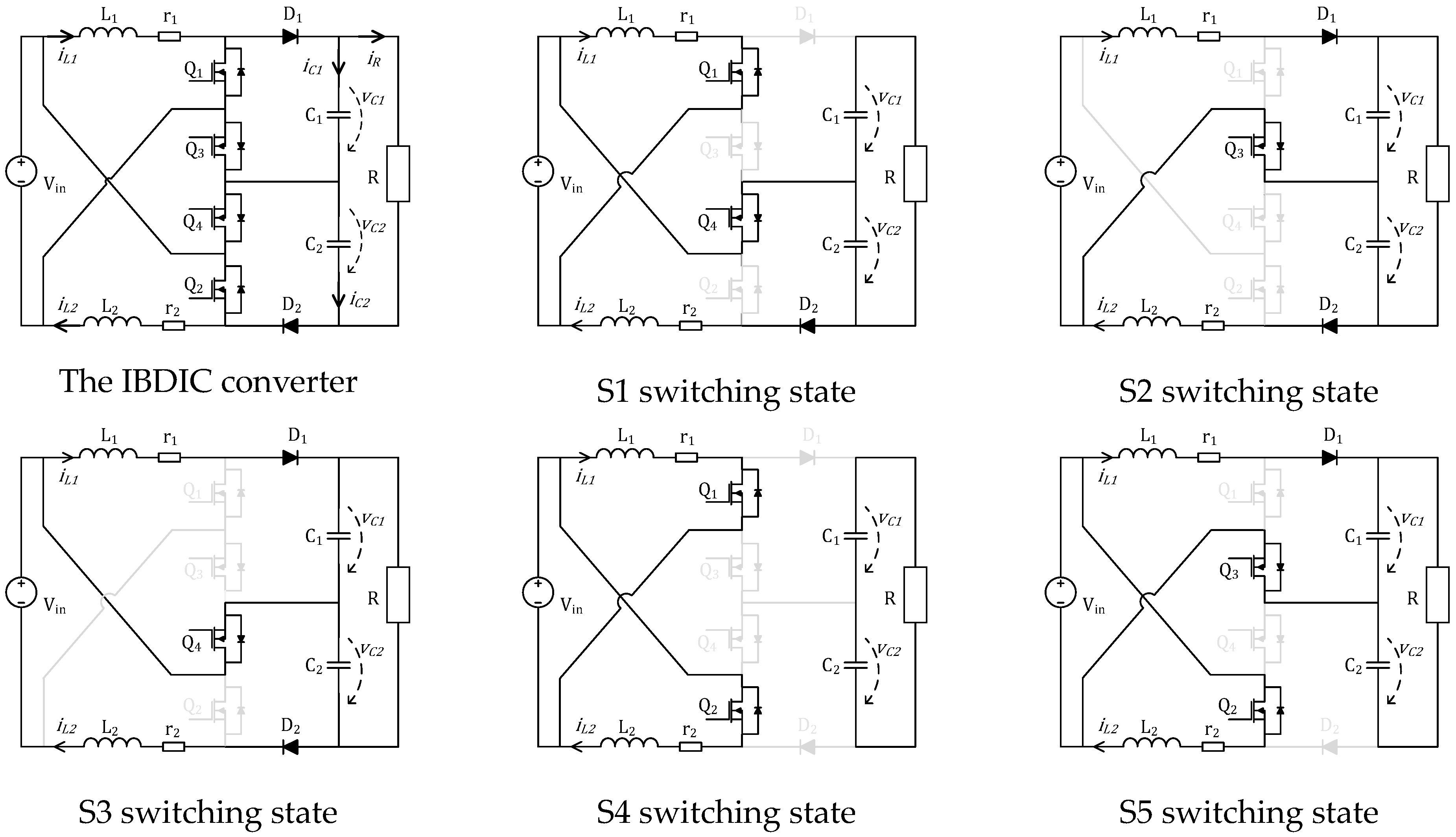
2.1. General Representation of the Switching States in CCM

In papers [13,14], the operation of the IDBIC converter is described and analyzed. Here, it is shown that the converter’s switching states and operation modes are influenced by the value of the duty cycle. Therefore, for CCM operation, the possible switching states of the converter are depicted in Figure 1. Moreover, in addition to the mentioned papers, the representations in Figure 1 include the equivalent series resistance (ESR) of the inductors for improved model accuracy.
For a duty cycle less than 50%, the switching states of the converter will be S1-S2-S5-S3, and in the case of the duty cycle exceeding 50%, the switching states will take the form of S4-S5-S4-S1 [13].

2.2. State-Space Average at CCM Operation and a Duty Cycle below 50%

Given the relationships between the state variables presented in [14], by inserting the inductors ESR, namely r 1 and r 2 , the system matrix of the converter for the S1 switching configuration will be described as follows:
A S 1 = r 1 L 1 0 0 0 0 r 2 L 2 0 1 L 2 0 0 1 R C 1 1 R C 1 0 1 C 2 1 R C 2 1 R C 2
Considering the S2 switching state, the resulting system matrix will be
A S 2 = r 1 L 1 0 1 L 1 0 0 r 2 L 2 0 1 L 2 1 C 1 0 1 R C 1 1 R C 1 0 1 C 2 1 R C 2 1 R C 2
For the final two switching states, the system matrices will be
A S 5 = r 1 L 1 0 1 L 1 0 0 r 2 L 2 0 0 1 C 1 0 1 R C 1 1 R C 1 0 0 1 R C 2 1 R C 2  
for the S5 state and
A S 3 = r 1 L 1 0 1 L 1 0 0 r 2 L 2 0 1 L 2 1 C 1 0 1 R C 1 1 R C 1 0 1 C 2 1 R C 2 1 R C 2
for the S3 state.
Given the duty cycle D and the matrices represented above, by averaging over one switching period, the system matrix, which describes the convertor operating at D < 0.5, results in
A α = A S 1 · D + A S 2 · 0.5 D + A S 5 · D + A S 3 · 0.5 D
where
A α = r 1 L 1 D 0 D 1 L 1 0 0 r 2 L 2 D 0 D 1 L 2 D C 1 0 2 D C 1 R 2 D C 1 R 0 D C 2 2 D C 2 R 2 D C 2 R

2.3. State-Space Average at CCM Operation and a Duty Cycle over 50%

In the situation when the converter operates with a duty cycle over 50%, the switching pattern differs. The specific state for this case is S4, which outputs the following system matrix:
A S 4 = r 1 L 1 0 0 0 0 r 2 L 2 0 0 0 0 1 R C 1 1 R C 1 0 0 1 R C 2 1 R C 2
By averaging over one switching period in this operating mode, the overall system matrix depicting the convertor will be characterized by
A β = A S 1   1 D + A S 5   1 D + A S 4   2 D 1
which results in
A β = r 1 1 L 1 0 D 1 L 1 0 0 r 2 1 L 2 0 D 1 L 2 1 D C 1 0 1 R C 1 1 R C 1 0 1 D C 2 1 R C 2 1 R C 2

3. The Condition Number Background

3.1. The Norm of a Matrix

The notion of a norm is presented in the context of distances between individual vectors or matrices, generalizing the concept of the absolute value of a scalar [15]. Matrix norms can be obtained in many ways [16]. An m × n matrix can be viewed as a vector in mn-dimensional space. Therefore, any mn-dimensional norm can be used for determining the “magnitude” of a such matrix. Considering matrix A as
A = a 11 a 12 a 1 n a 21 a 22 a 2 n a n 1 a n 2 a n n
The norm of A will be
A = m a x a 11 + + a 1 n ;   ;   | a n 1 | + + | a n n |  
Therefore, it is described as the maximum value obtained by summing the absolute values of each row [17].
It is worth mentioning that other vector-induced norms that are common are the so-called “p-norms”, represented as A p , where 1 p < . Among these, A 1 , known as the 1-norm, and A 2 , known as the 2-norm or Euclidean norm, are the most common. The 1-norm is obtained in a similar manner to A , only summing, instead, the absolute values of the elements for each column. The 2-norm is harder to compute, and it is determined by the sqrt of the largest eigenvalue of A T A . Due to the structure of the state-space representation of the converter, A is most suitable for use in the computations, as it can be correlated for each state variable [18].

3.2. The Condition Number of a Matrix

In the field of numerical methods, the condition number of a problem is defined as the maximum error magnification over all input changes, or at least all changes of a prescribed type. The condition number of square matrix A is the maximum possible error magnification factor for solving A · x = M ,= for all right-hand sides M [17], and it is described as follows:
c o n d A = A · A 1
where A is the norm of the A matrix.
Therefore, matrix A is well conditioned if c o n d ( A ) is close to 1 and ill conditioned when c o n d ( A ) is significantly greater than 1. Conditioning, in this context, refers to the relative security that a small residual vector implies a correspondingly accurate approximate solution [18]. In non-mathematical terms, a poorly conditioned matrix is one in which, for a small change in inputs (independent variables), there is a large change in the response or dependent variable. This means that the correct solution/answer to the equation described by that matrix becomes hard to find. However, with the development of complex mathematical software such as MATLAB and others, an estimate of the condition number is often available.

4. The Converter’s Condition Number

Since the state matrix describing the converter is a square matrix, it is believed to determine its condition number and observe how it could be used to describe the behavior of the system. To determine the condition number, it is necessary to calculate the norm of the averaged state matrix and the norm of its inverse, as suggested in relation (12). As the state matrix differs according to the duty cycle, the condition number will be determined for each situation when its value is below and above 50%.

4.1. Converter with a Duty Cycle below 50%

With the help of the symbolic math library in MATLAB, the norm of the A α matrix, which is presented in relation (6), was determined. Its representation is depicted in relation (13).
A α = max a ; b ; c ; d   where   a = r 1 L 1 + 1 D L 1 ; b = r 2 L 2 + 1 D L 2 ; c = D C 1 + 4 · D C 1 R ; d = D C 2 + 4 · D C 2 R
In a similar manner, the norm of the inverse of A α was determined, as shown in relation (14):
A α 1 = max m ; n ; o ; p   where   m = 2 · D L 1 + L 2 + 2 · C 2 r 2 + C 1 2 r 2 + R 1 D D · 2 r 1 + r 2 + R 1 D ; n = 2 · D L 1 + L 2 + 2 · C 1 r 1 + C 2 2 r 1 + R 1 D D · 2 r 1 + r 2 + R 1 D ; o = D · 2 L 2 r 1 + L 1 2 r 2 + R 1 D + | r 1 | · 2 C 2 r 2 + C 1 2 r 2 + R 1 D D · R + 2 r 1 + r 2 2 D r 1 + r 2 + R D 2 D p = D · 2 L 2 r 2 + L 2 2 r 1 + R 1 D + | r 2 | · 2 C 1 r 1 + C 2 2 r 1 + R 1 D D · R + 2 r 1 + r 2 2 D r 1 + r 2 + R D 2 D
As the norms of the matrices depend on the maximum value found in expressions (13) and (14), a simplification of the mathematical relations is intended. Given that in a practical implementation [13], the converter will have a symmetrical construction, the values of some components will coincide. Maintaining the overall approximation in a tolerable limit, the following can be concluded:
  • All values of the circuit’s components are positive;
  • Considering the differences between the values of the same type of component are very small, it can be approximated that L 1 = L 2 = L , C 1 = C 2 = C and r 1 = r 2 = r ;
  • Operating at a duty cycle smaller than 50% results in 0 < D 0.5 .
Applying these approximations to each of the norm elements in (13) and (14), it can be observed that the terms are two by two equal. By writing in (13), a = b = x 1 α and c = d = x 2 α , and by writing in (14): m = n = y 1 α and o = p = y 2 α , resulting in
A α = max x 1 α ; x 2 α   where   x 1 α = r + 1 D L x 2 α = D ( R + 4 ) C R
and
A α 1 = max y 1 α ; y 2 α     where   y 1 α = 4 D L + C r + C R 1 D D 4 r + R 1 D y 2 α = ( D L + C r ) 4 r + R ( 1 D ) D 4 r 1 D + R 1 D 2
To determine A α and A α 1 , a series of operations are conducted. It is noted that the operations and simplifications are applied identical to both terms of each norm. Therefore, the following is true:
  • To establish the maximum between x 1 α and x 2 α , both terms are multiplied by C / ( r + 1 D ) , which results in
    A α = max C L ;   D r + 1 D · R + 4 R
  • Knowing that, in practice [13], R 4 , the R + 4 R 1 approximation is made. The relation through which the maximum is defined results in
    C L   v s . D r + 1 D
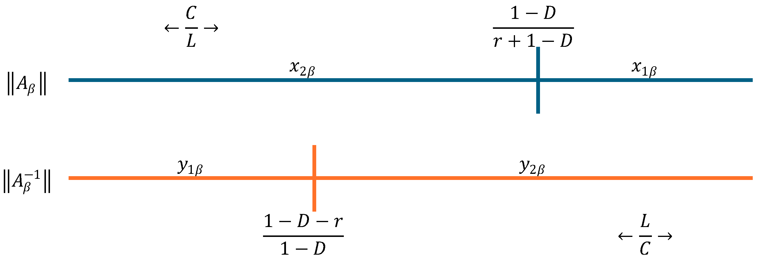
  • In relation (18), we can observe that the norm of the system matrix, hence the condition number, depends on the ratio between the capacitor and inductor values with respect to the duty cycle. By taking into consideration the left-hand/right-hand side positioning of the terms in relation (18) and the order of the terms in relation (15), the norm of A α is obtained as follows:
    i f C L > D r + 1 D   A α = x 1 α C L < D r + 1 D   A α = x 2 α
  • In an equivalent manner, the maximum between y 1 α and y 2 α is determined. After obtaining a common denominator, the numerators of y 1 α and y 2 α are observed for establishing A α 1 , as shown in relation (20):
    A α 1 = max C L + r · C D ;   R 4 R + 4 r R ( 1 D ) · D 1 D
  • Considering that a small value of r is desired, the approximation r < 1 will be made. As such, in a practical application [13], we consider that R 4 and R r result in ( R 4 ) / R + 4 r / ( R ( 1 D ) ) 1 . After some operations, the relation from which the maximum value is derived stands as
    C L v s . D 1 D · C L · r D + 1
  • In this situation, the norm of the inverse matrix is also defined by the capacitor and inductor values ratio and the duty cycle. Considering the positioning of the maximum in relation (21) and the terms in relation (16), the norm of A α 1 results in
    i f C L > D 1 D · C L · r D + 1   A α 1 = y 1 α C L < D 1 D · C L · r D + 1   A α 1 = y 2 α
When the ESR value r is ignored, relations (19) and (22) become identical for both instances. The condition number is then obtained as follows:
c o n d A α = x 1 α · y 1 α ,     C L > D 1 D x 2 α · y 2 α ,     C L < D 1 D
If the value of r is taken into consideration, the starting points are relations (18) and (21). Here, because the left-hand term is the same in both cases, the sequence of the right-hand terms is of interest. Considering that r > 0 and 0 < D 0.5 , it can be deduced that
D 1 D · 1 D r + 1 D < D 1 D < D 1 D · C L · r D + 1
In Figure 2, a graphical representation based on relation (24) is illustrated. The intervals defined by the C / L ratio are specific to each matrix norm and depicted in blue for A α and orange for A α 1 .
The ratio is evaluated at the same time for each of the intervals. Therefore, depending on the value of the ratio, the condition number of the A α matrix can be determined as follows:
c o n d A α = x 2 α · y 2 α ,     C L < D 1 D · 1 D r + 1 D x 1 α · y 2 α ,     C L > D 1 D · 1 D r + 1 D x 1 α · y 1 α ,     C L > D 1 D · C L · r D + 1

4.2. Converter with a Duty Cycle above 50%

When operating at a duty cycle greater than 50%, the average state system matrix of the converter is determined in relation (9). With the help of the MATLAB symbolic toolbox, the norms of A β and A β 1 are determined. As in the previous situation, to simplify the norms’ expressions, a series of approximations and assumptions based on a practical implementation [13] are necessary. Therefore, all circuit elements have positive values, and the same type of elements have identical values. Considering that 0.5 D < 1 , results in
A β = max x 1 β ; x 2 β   where   x 1 β = r + 1 D L x 2 β = 2 + R 1 D C R
and
A β 1 = max y 1 β ; y 2 β     where   y 1 β = C 1 D + 2 L R 1 D 2 + 2 r y 2 β = L 1 D + C r 1 D 2
To determine the maximum value between x 1 β and x 2 β , both terms are multiplied with C / ( r + 1 D ) , with the result that in a practical implementation [13], R 2 . In this sense, the maximum is identified via the comparison of
C L v s . 1 D r + 1 D
As previously stated, the norm of the matrix depends on the ratio of the capacitor and inductor values with respect to the duty cycle. By keeping track of the position of the terms in relation (28) and the order of the terms in the norm in expression (26), it can be concluded that
i f C L > 1 D r + 1 D A β = x 1 β C L < 1 D r + 1 D A β = x 2 β
The norm of the inverse matrix is deduced by comparing y 1 β and y 2 β . After simplifying the relations and noting that R 2 , the relation from which the maximum between the two terms is established is
1 D r 1 D v s . L C
It can be noted that in this case, the inverse of the ratio is taken into consideration when establishing the matrix norm. Therefore, by comparing the elements in relation (30) and correlating the maximum value obtained with the position of the terms in expression (27), we can conclude that
i f L C < 1 r 1 D A β 1 = y 1 β L C > 1 r 1 D A β 1 = y 2 β
A visual interpretation of relations (29) and (31) is represented in Figure 3. Here, the two intervals depict the values of the norms, with blue for A β and orange for A β 1 .
To establish the condition number matrix A β , the possible norm values combination must be determined. A series of observations can provide aid in this manner, such as the following:
  • The values of the ratios C / L and L / C are positive
  • The values of r and D are defined as 0 r < 1 and 0.5 D < 1 ;
Taking into consideration the previous observations, it can be concluded that
  • ( 1 D ) / ( r + 1 D ) has a positive value, less or equal to 1;
  • ( 1 D r ) / ( 1 D ) has a value less than or equal to 1, and it can be a negative value;
  • y 1 β can be a negative value, in which case it cannot be a valid solution for the norm;
  • By analyzing the possible norm values, the condition number of the A β matrix can be determined as follows:
    c o n d A β x 1 β · y 1 β   , C L > 1 D r + 1 D   a n d   L C < 1 r 1 D x 2 β · y 2 β   , C L < 1 D r + 1 D   a n d   L C > 1 r 1 D   x 1 β · y 2 β   , C L > 1 D r + 1 D   a n d   L C > 1 r 1 D

5. The Behavior of the Condition Number

Relations (25) and (32) will be evaluated to observe the behavior of the condition number of the converter’s system matrix. By changing the value of the C / L ratio, a series of graphic representations will be made for the various cases of the converter operation.

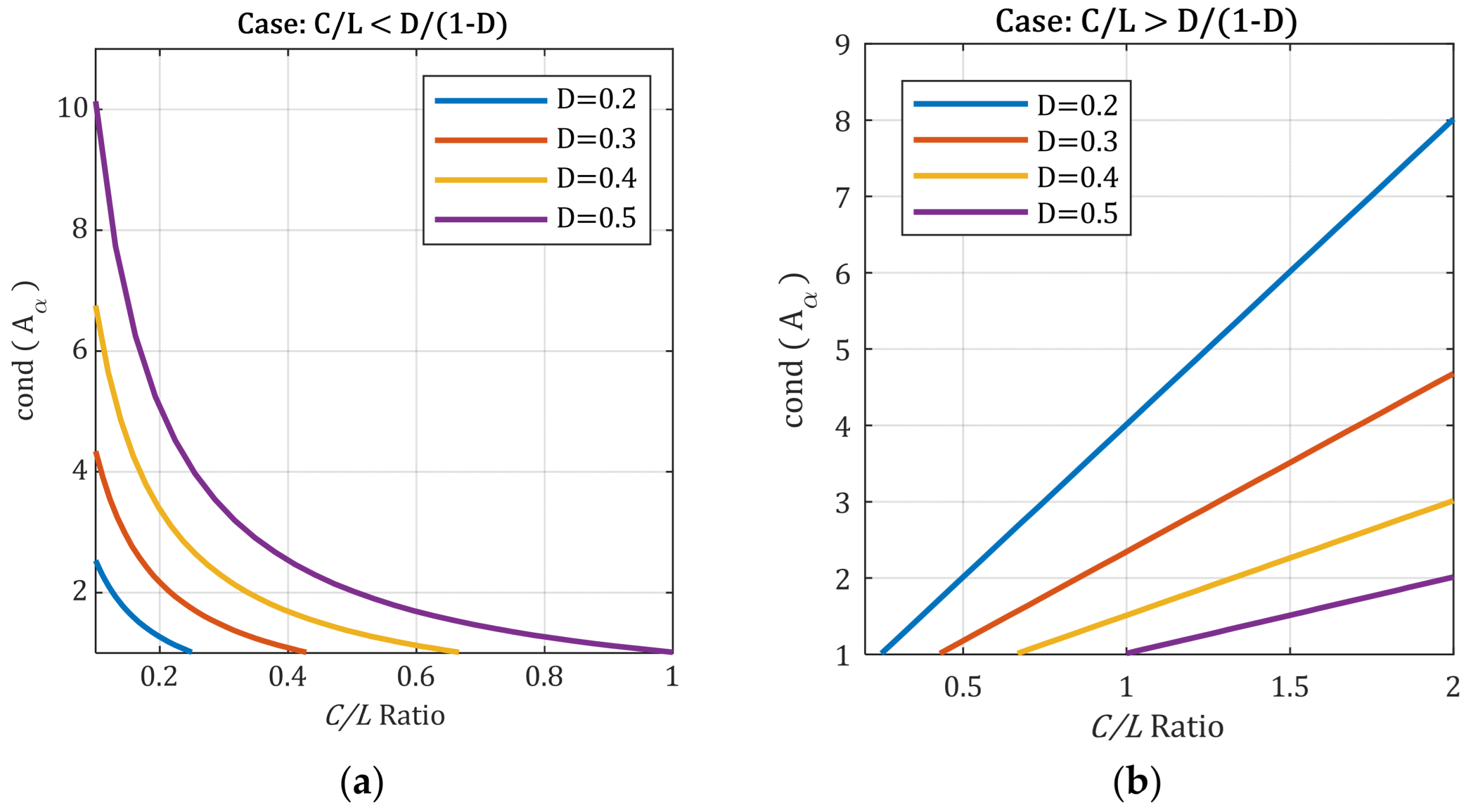
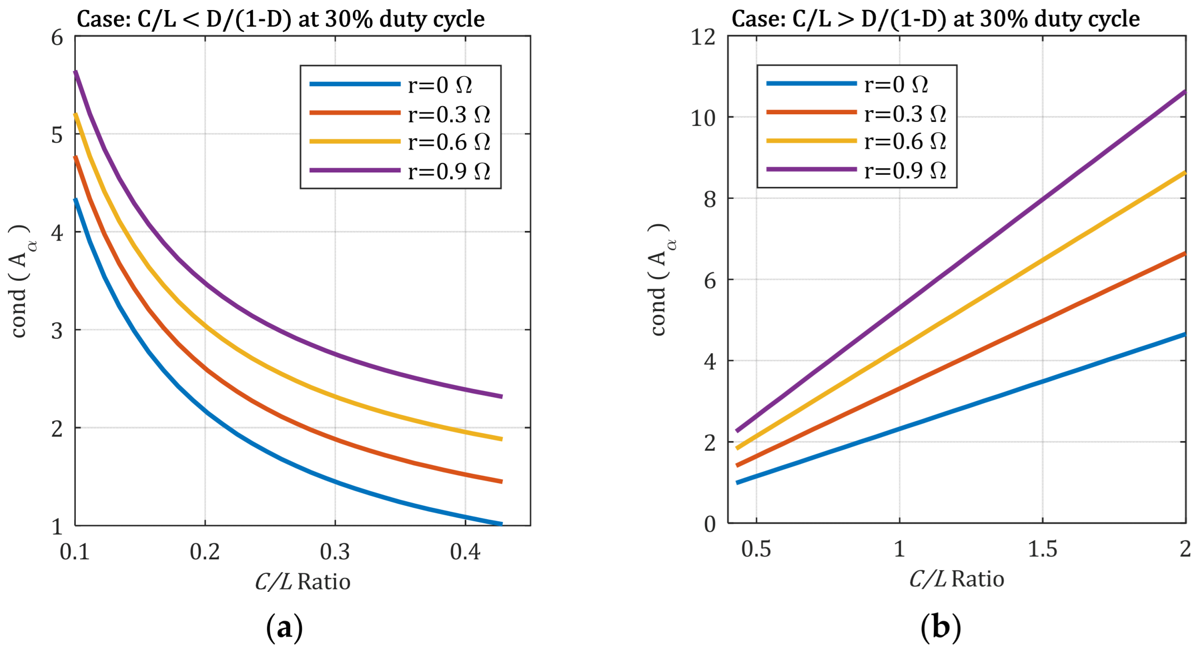
5.1. Converter Operating below a 50% Duty Cycle

In Figure 4, the variation in the condition number of A α is represented, specifically for the converter operating at a duty cycle less than 50%. Here, the inductor’s ESR is neglected; therefore, r = 0 . As can be seen, depending on the ratio of the capacitor and inductor values, at different duty cycles, c o n d ( A α ) has a different behavior. When discussing the relevance of the condition number in Section 3 of this paper, it has been mentioned that a small condition number value that is close to 1 should be of interest. The C / L ratio takes values from 0 to 1 in Figure 4a and values from 1 to 2 in Figure 4b.
In Figure 4a, the condition number greatly increases as the C / L ratio decreases. There are, however, points at which its value becomes unity, but they depend on the duty cycle. In Figure 4b, the variation in c o n d ( A α ) is linear, increasing with the C / L ratio. In both situations, for a specific duty cycle D , the values of the capacitors and inductors utilized in the converter configuration can be optimized to obtain a smaller value for the condition number.
In a physical implementation, the inductor’s ESR will be greater than zero. Nonetheless, a small value will be convenient. In this manner, the variation in c o n d A α for a series of different values of r is represented in Figure 5. To reduce the complexity of the representation, the duty cycle’s value is set to D = 0.3 in relation (25).
As can be observed, the overall behavior of the condition number is similar to the one presented in Figure 4. However, by considering the presence of the inductor’s ESR, we can observe that the unity value is no longer obtained. The difference in the variation in c o n d ( A α ) is specific for each value of r in Figure 5a, as well as in Figure 5b.

5.2. Converter Operating above a 50% Duty Cycle

Considering relation (32) and the representation shown in Figure 3, the variation in c o n d ( A β ) for the ideal case when r = 0 , is presented in Figure 6. In this situation, the interval-limiting expressions represented in Figure 3 are identical and equal to 1. Despite the different values of the duty cycle, the behavior of the condition number is relatively similar for all the values. In Figure 6a, the representation corresponds to the sub-unitary values of the C / L ratio, while in Figure 6b, the values of the ratio are greater than 1.
Taking into consideration the series resistance of the converter’s inductors, the variations in c o n d ( A β ) are presented in Figure 7. Here, the condition number’s behavior is particular to each value of r , with the duty cycle being set at 60%.
In Figure 7a, the C / L ratio is sub-unitary. When compared to the representation from Figure 5a,b, we can observe that the abrupt change in the condition number’s variation does not occur at the same C / L ratio in this case. In addition, this aspect determines a larger deviation of c o n d ( A β ) for a C / L ratio greater than 1, as can be seen in Figure 7b.
As in previous situations, with the inductor’s ESR taken into consideration, the unity value for the condition number is no longer achievable. Furthermore, the overall behavior remains similar to the one for when the duty cycle is less than 50%.

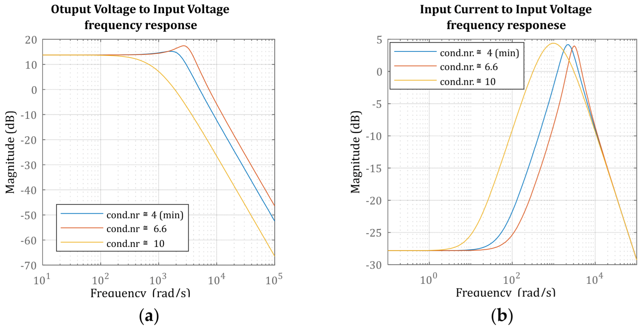
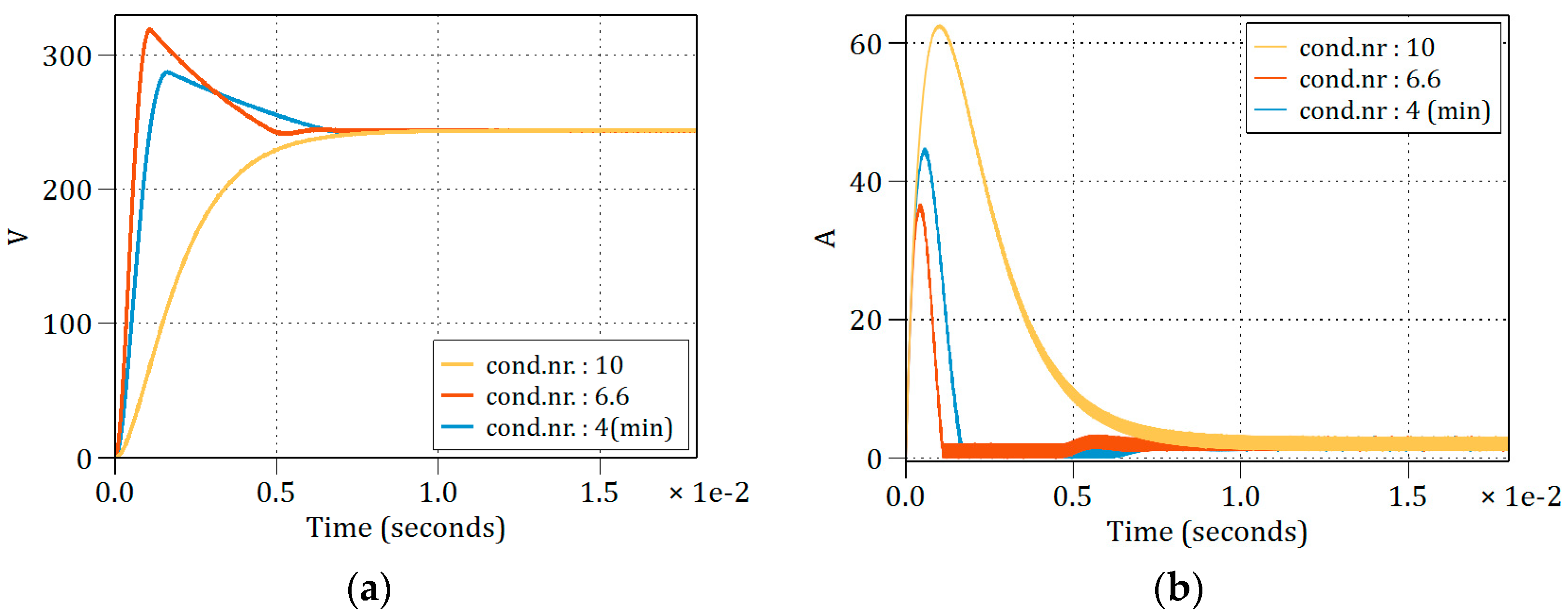
6. The Condition Number and the Converter’s Performance

Having determined the manner in which the converter’s condition number is correlated to its passive elements and the duty cycle, a brief analysis of the converter’s behavior is proposed. With reference to Figure 7, the behavior of the converter’s condition number for the inductor ESR of r = 0.6   Ω at a duty cycle of 60% is represented in Figure 8.
It is worth mentioning that in order for the converter to operate in CCM, a suitable value for the inductor L must be selected [13]. As mentioned before, in order to modify the condition number, different values of the capacitance C are chosen, which will influence the C / L ratio. By doing so, in Figure 8, we notice that there is a minimum value for the condition number variation. An analysis of the converter’s behavior in this situation and a comparison with some circumstances of non-minimum values is undertaken in order to observe any particularities that might occur.
By using relations (26), (27) and (32), the converter’s condition number was determined for different values of the C / L ratio. The values were chosen with the aim of emphasizing the effect of the minimum and two more extreme points on the representation in Figure 8. Therefore, C / L ratios of 0.2, 0.4 and 2 will output the condition numbers of 6.6, 4 (minimum) and 10.
Based on the output-to-input voltage transfer function and on input current-to-input voltage transfer function, which can be derived from the model of the converter in [14], a frequency response plot is presented in Figure 9.
When evaluating the frequency responses, it is noted that the bandwidth varies with the condition number. Therefore, in Figure 9a, as the condition number increases, the output voltage response bandwidth changes in an irregular fashion. The same observation can be made for the bandwidth of the input current in Figure 9b. Consequently, for the same value of the condition number, either the voltage response has a smaller bandwidth and the current response has a larger bandwidth, or vice-versa, all with respect to the response corresponding to the minimum value of the converter’s condition number. Hence, by observing this aspect, the possibility that the condition number can be used as a convergent point to facilitate a behavioral analysis of the converter is emphasized.
Based on the same transfer functions, the open-loop response of the converter to a 50 V step input is presented in Figure 10.
Key aspects of the simulated model should be mentioned: the inductors L 1 and L 2 have values corresponding to the converter operating in CCM [13], the inductor ESR resistors r 1 and r 2 are 0.6 Ω , the load R remains constant, the input voltage V is 50 V and the duty cycle is 60%. The only variable parameter is the value of C 1 and C 2 , and it will correspond to a specific C / L ratio in order to match the previously mentioned condition number values for the converter.
Once again, the converter’s configuration was predefined for obtaining the same condition number values. Here, it can also be observed that for values different from the minimum, the output voltage or input current step responses are not simultaneously favorable. In this manner, the voltage step response, depicted in Figure 10a for the converter with a condition number equal to 10, is overdamped, reaching the steady-state value with no voltage overshoot. On the other hand, the step response of the input current has a large overshoot, for the exact same value of the condition number, as seen in Figure 10b. The case when the current in Figure 10b has the least amount of overshoot corresponds to a converter configuration that yields a condition number with a value of approximately 6.6. However, for the same situation, the voltage response in Figure 10a has the least desirable transient evolution, with the largest overshoot.
Considering the voltage and current step response for when the converter’s configuration produces the minimum value for the condition number, in Figure 10a,b, each response manages to compromise the optimum transient behavior for both the output voltage and the input current. Therefore, the responses simultaneously have the least amount of overshoot among the other possible configurations.
In order to observe the correlation between the condition number and its behavior, an open-loop simulation of the converter was made using PLECS software. The simulation model is presented in Figure 11.
The simulation starts by applying the input voltage to the converter, with all-zero initial conditions. The measured outputs are the inductor current and the output voltage. The results are illustrated in Figure 12. As in the previous case, three simulations were undertaken for the C / L ratios of 0.2, 0.4 and 2. The behavior of the output voltage and inductor current is similar to the one presented in Figure 10. The idea that the minimum value of the condition number, hence the corresponding C / L ratio, delivers the best compromise regarding the open-loop response of the converter is also emphasized here. The transient behaviors of the output voltage in Figure 12a and the inductor current in Figure 12b underline this concept.
Although the practical implementation and performance benchmarking of the IDBIC converter are presented thoroughly in [13], for the purpose of this paper, relying just on the open-loop simulation helps to emphasize the idea of the condition number’s influence over the switching behavior of the converter. Considering that the current paper has a theoretical approach, observing the simulated results of the converter’s response can conclude that in the case of a switching model, the response adheres to the one anticipated by the proposed theoretical method, as presented in this paper. Understandably, the simulated circuit is partially idealized with regard to some aspects such as the lack of voltage drop across the semiconductor devices or lack of switching losses and conduction losses. These might lead to disparities regarding eventual experimental outcomes concerning things such as the gain or settling time of the observed parameters. Even so, the concept of the optimum converter response being connected to the minimum value of its condition number is not undermined by this approach, being primarily dependent on the capacitor and inductor values, as discussed and demonstrated before.

7. Conclusions

In this paper, a novel approach to observing the behavior of an electronic converter is proposed. The method evaluates the condition number of the state matrix of the converter in order to assess the possibility of integrating it in the design stage. After establishing the state matrices of the converter, a series of assumptions and approximations based on its operation are made. With this step, the mathematical relations for the norms and condition numbers of the state matrix for each of the converter’s operation modes are derived. It is shown how the condition number depends on the passive elements present in the converter’s topology and how the duty cycle at which the converter operates influences this measure.
The possibility of obtaining a correlation between the condition number and the converter’s behavior is considered Hence, by observing the open-loop response of the converter for different values of its condition number, an association between the minimum value of the condition number and the optimal tradeoff regarding the converter’s response has been identified, thus providing an additional tuning element in the design stage of the converter.
For the future development of this work, observations regarding the condition number’s influence on the behaviors of other types of electronics converters topologies are of interest. Furthermore, analyzing the corresponding circuit parameters that characterize the condition number for the different topologies, together with the idea of obtaining a systemic description of the condition number, for a group of interconnected or parallel-fed converters will be considered.

Author Contributions

Conceptualization, S.I.S. and V.M.S.; methodology, S.I.S.; validation V.M.S. and P.D.T.; formal analysis, P.D.T.; investigation, S.I.S.; writing—original draft preparation, S.I.S. and V.M.S.; writing—review and editing, S.I.S. and P.D.T.; supervision, P.D.T.; project administration, P.D.T. and Z.M.; funding acquisition, Z.M. All authors have read and agreed to the published version of the manuscript.

Funding

This study was co-funded by the European Regional Development Fund through the Competitiveness Operational Program 2014–2020 Romania, grant number no. 437/390113/17.02.2023, cod. SMIS 156450, project title “The development of an innovative electronic system for collecting energy from renewable sources—SEICER”.

Data Availability Statement

Data is contained within the article.

Conflicts of Interest

The authors declare no conflicts of interest.

References

  1. Yan, D.; Yang, C.; Hang, L.; He, Y.; Luo, P.; Shen, L.; Zeng, P. Review of General Modeling Approaches of Power Converters. Chin. J. Electr. Eng. 2021, 7, 27–36. [Google Scholar] [CrossRef]
  2. Yue, X.; Wang, X.; Blaabjerg, F. Review of Small-Signal Modeling Methods Including Frequency-Coupling Dynamics of Power Converters. IEEE Trans. Power Electron. 2019, 34, 3313–3328. [Google Scholar] [CrossRef]
  3. Burdio, J.M.; Martinez, A.; Garcia, J.R. Derivation of Some Classical Modeling Methods for Power Electronic Converters from a Unified Model. In Proceedings of the PESC Record—27th Annual IEEE Power Electronics Specialists Conference, Baveno, Italy, 23–27 June 1996; IEEE: New York, NY, USA; Volume 2, pp. 1382–1387. [Google Scholar]
  4. Caliskan, V.A.; Verghese, O.C.; Stankovic, A.M. Multifrequency Averaging of DC/DC Converters. IEEE Trans. Power Electron. 1999, 14, 124–133. [Google Scholar] [CrossRef]
  5. Kwon, J.B.; Wang, X.; Bak, C.L.; Blaabjerg, F. Modeling and Simulation of DC Power Electronics Systems Using Harmonic State Space (HSS) Method. In Proceedings of the 2015 IEEE 16th Workshop on Control and Modeling for Power Electronics (COMPEL), Vancouver, BC, Canada, 12–15 July 2015; IEEE: New York, NY, USA; pp. 1–8. [Google Scholar]
  6. Jaen, C.; Pindado, R.; Pou, J.; Sala, V. Adaptive Model Applied to PWM DC-DC Converters Using Averaging Techniques. In Proceedings of the 2006 IEEE International Symposium on Industrial Electronics, Montreal, QC, Canada, 9–13 July 2006; IEEE: New York, NY, USA; pp. 1347–1352. [Google Scholar]
  7. Meher, T.; Majhi, S.; Ramana, K.V. Hammerstein Modeling of Buck Converter Using Relay Feedback. In Proceedings of the TENCON 2019—2019 IEEE Region 10 Conference (TENCON), Kochi, India, 17–20 October 2019; IEEE: New York, NY, USA; pp. 637–642. [Google Scholar]
  8. Shah, C.; Vasquez-Plaza, J.D.; Campo-Ossa, D.D.; Patarroyo-Montenegro, J.F.; Guruwacharya, N.; Bhujel, N.; Trevizan, R.D.; Rengifo, F.A.; Shirazi, M.; Tonkoski, R.; et al. Review of Dynamic and Transient Modeling of Power Electronic Converters for Converter Dominated Power Systems. IEEE Access 2021, 9, 82094–82117. [Google Scholar] [CrossRef]
  9. Alcaide, A.M.; Buticchi, G.; Chub, A.; Dalessandro, L. Design and Control for High-Reliability Power Electronics: State-of-the-Art and Future Trends. IEEE J. Emerg. Sel. Top. Ind. Electron. 2024, 5, 50–61. [Google Scholar] [CrossRef]
  10. Kim, M.; Yun, H.-J. A Basic Design Tool for Grid-Connected AC–DC Converters Using Silcon Carbide MOSFETs. Electronics 2023, 12, 4828. [Google Scholar] [CrossRef]
  11. Hinov, N.; Gocheva, P.; Gochev, V. Index Matrix-Based Modeling and Simulation of Buck Converter. Mathematics 2023, 11, 4756. [Google Scholar] [CrossRef]
  12. Ebrahimian, R.; Baldick, R. State Estimator Condition Number Analysis. IEEE Trans. Power Syst. 2001, 16, 273–279. [Google Scholar] [CrossRef]
  13. Suciu, V.M.; Salcu, S.I.; Pacuraru, A.M.; Pintilie, L.N.; Szekely, N.C.; Teodosescu, P.D. Independent Double-Boost Interleaved Converter with Three-Level Output. Appl. Sci. 2021, 11, 5993. [Google Scholar] [CrossRef]
  14. Szekely, N.C.; Salcu, S.I.; Suciu, V.M.; Pintilie, L.N.; Fasola, G.I.; Teodosescu, P.D. Power Factor Correction Application Based on Independent Double-Boost Interleaved Converter (IDBIC). Appl. Sci. 2022, 12, 7209. [Google Scholar] [CrossRef]
  15. Ascher, U.M.; Greif, C. A First Course in Numerical Methods; Society for Industrial and Applied Mathematics: Philadelphia, PA, USA, 2011; ISBN 978-0-89871-997-0. [Google Scholar]
  16. Trefethen, L.N.; Bau, D. III. Numerical Linear Algebra; Society for Industrial and Applied Mathematics: Philadelphia, PA, USA, 1997; ISBN 0-89871-361-7. [Google Scholar]
  17. Sauer, T. (Ed.) Numerical Analysis, 2nd ed.; Pearson: Boston, MA, USA, 2012; ISBN 978-0-321-78367-7. [Google Scholar]
  18. Burden, A.M.; Faires, J.D.; Burden, R.L. Numerical Analysis, 10th ed.; Cengage Learning: Boston, MA, USA, 2016; ISBN 978-1-305-25366-7. [Google Scholar]
Figure 1. Switching states of the IBDIC converter operating in CCM.
Electronics 13 01302 g001
Figure 2. The norms’ elements considering the C / L ratio at a duty cycle below 50%.
Electronics 13 01302 g002
Figure 3. The norms’ elements considering the C / L ratio at a duty cycle above 50%.
Electronics 13 01302 g003
Figure 4. Converter’s condition number behavior with respect to C / L ratio at duty cycles less than 50%, without the inductor’s ESR: (a) C / L value less than D / ( 1 D ) ; (b) C / L value larger than D / ( 1 D ) .
Electronics 13 01302 g004
Figure 5. Converter’s condition number behavior with respect to the C / L ratio at a 30% duty cycle, considering the inductor’s ESR: (a) C / L value less than D / ( 1 D ) ; (b) C / L value larger than D / ( 1 D ) .
Electronics 13 01302 g005
Figure 6. Converter’s condition number behavior with respect to the C / L ratio at duty cycles above 50%, without the inductor’s ESR: (a) C / L value less than 1; (b) C / L value larger than 1.
Electronics 13 01302 g006
Figure 7. Converter’s condition number behavior with respect to the C / L ratio at a 60% duty cycle, considering the inductor’s ESR: (a) C / L value less than 1; (b) C / L value larger than 1.
Electronics 13 01302 g007
Figure 8. IDBIC converter’s condition number behavior with respect to the C / L ratio at a 60% duty cycle and inductor ESR of 0.6   Ω .
Electronics 13 01302 g008
Figure 9. Frequency response of the IDBIC converter for different instances of the converter’s condition number: (a) output voltage with respect to the input voltage; (b) input current with respect to the input voltage.
Electronics 13 01302 g009
Figure 10. IDBIC converter’s response to a 50 V step input for different values of the condition number: (a) output voltage response; (b) input current response.
Electronics 13 01302 g010
Figure 11. The PLECS simulation model of the IDBIC converter.
Electronics 13 01302 g011
Figure 12. Open-loop simulation results for the IDBIC converter for different condition number configurations: (a) output voltage; (b) inductor current.
Electronics 13 01302 g012
Disclaimer/Publisher’s Note: The statements, opinions and data contained in all publications are solely those of the individual author(s) and contributor(s) and not of MDPI and/or the editor(s). MDPI and/or the editor(s) disclaim responsibility for any injury to people or property resulting from any ideas, methods, instructions or products referred to in the content.

