Article

On the Use of Ridge Waveguides to Synthesize Impedances

by
Juan J. Flórez Rodríguez
* and
Luis F. Herrán
Polytechnic School of Engineering of Gijón, University of Oviedo, 33003 Oviedo, Spain
*
Author to whom correspondence should be addressed.
Electronics 2025, 14(6), 1060; https://doi.org/10.3390/electronics14061060
Submission received: 13 February 2025 / Revised: 3 March 2025 / Accepted: 5 March 2025 / Published: 7 March 2025
(This article belongs to the Special Issue Microwave Devices: Analysis, Design, and Application)

Abstract

:
This work examines the feasibility of designing an impedance synthesis network based on a double-ridge waveguide (DRW). This design is based on the concept of the stepped-impedance line transformer as a cascade of transmission lines with different characteristic impedances, but using, in this particular case, a stepped-ridge waveguide. It is shown that this structure is able to synthesize not only real impedances but an arbitrary impedance, following some restrictions explained in this paper. An impedance synthesis network based on DRW can have numerous applications, like being used in designing amplifiers, which would eventually make possible to integrate amplifiers in waveguide technology.

1. Introduction

Impedance synthesis is a fundamental process in the design of many active components, such as amplifiers or oscillators. In the case of amplifiers, it is well known that achieving specific reflection coefficients at both input and output is necessary to make them provide a specific gain value with acceptable return losses. This implies the use of impedance synthesis networks, but these are usually implemented in microstrip substrates by using stubs [1] or lumped elements [2]. This technology shows a lower efficiency in terms of propagation losses, especially when working at high frequencies, like those in 5G bands. In that case, rectangular waveguides (RWGs) and RWG-based structures play a crucial role because of their low losses compared with other structures. In this sense, ridge waveguides (RWs) [3] are even more useful due to their enhanced bandwidth with respect to RWGs [4]. This is because the separation between the first- and second-order modes is wider than that associated with an RWG. The main parameters of a double-ridge waveguide (DRW) are shown in Figure 1.
The reason why this impedance synthesis network is presented in this paper is that the ultimate goal is being able to integrate an amplifier with waveguide technology, particularly on a DRW. As impedance synthesis plays that important role, this paper dives into the analysis of a DRW and its viability to work as an impedance synthesis network.
There are several works that design impedance synthesis networks solely for matching purposes and using lumped elements [5]. Some of them use DRW or RW-to-microstrip or substrate-integrated waveguide (SIW) transitions [6,7,8,9]. However, all of them are designed to obtain real impedances and mostly use a stepped-ridge waveguide as a transition but again not for impedance synthesis purposes. Moreover, to the best of our knowledge, no circuits have been designed or implemented to synthesize not only real but also complex impedances on DRWs up to now. In this paper, the impedance synthesis network is built on a DRW instead of the most common single-ridge waveguide (SRW) because it would be a better option in terms of having both ridges providing mechanical support for an eventual transistor working as an amplifier with both stepped-ridges being the impedance synthesis networks.
In this paper two different circuits were designed and manufactured to demonstrate the capability of DRWs to synthesize arbitrary complex impedances.

2. Materials and Methods

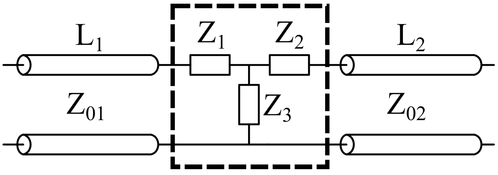
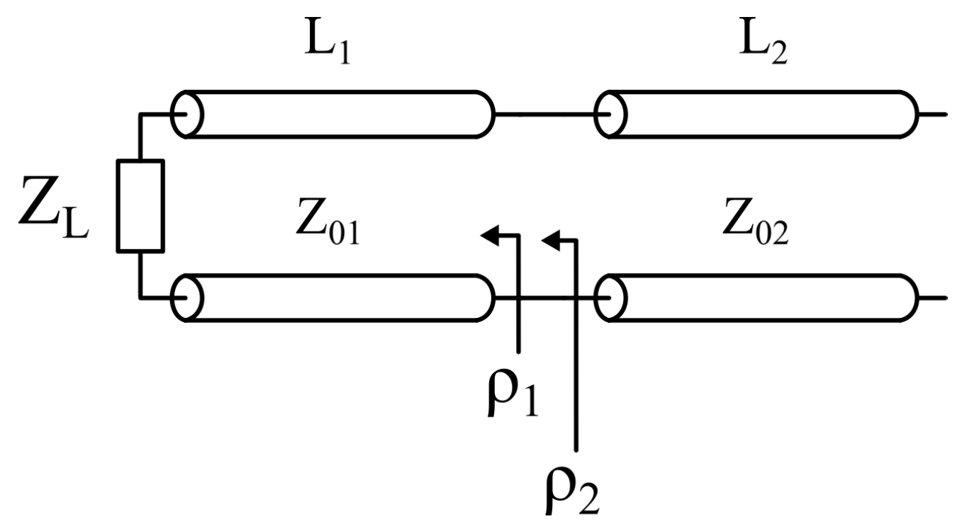
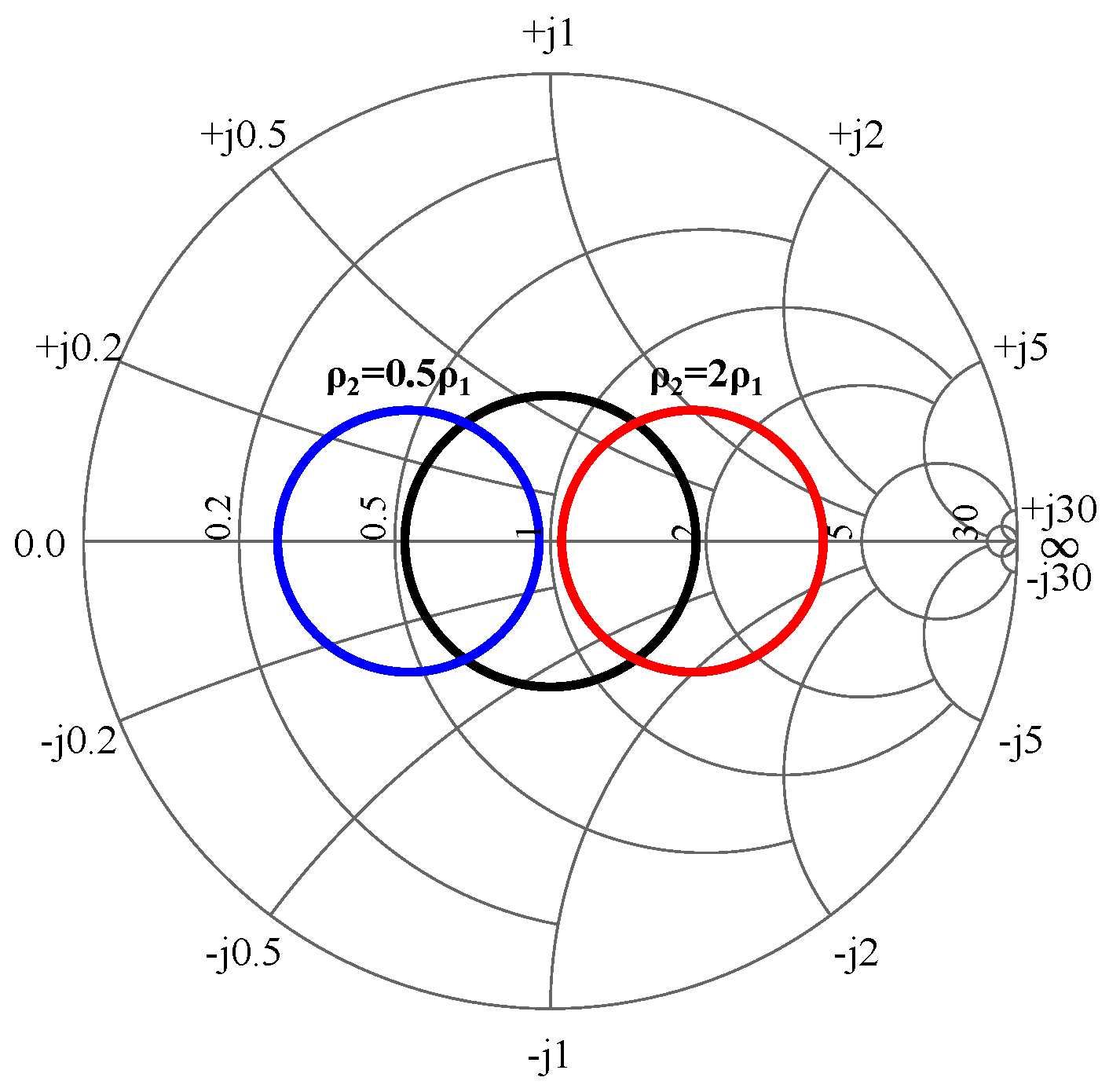
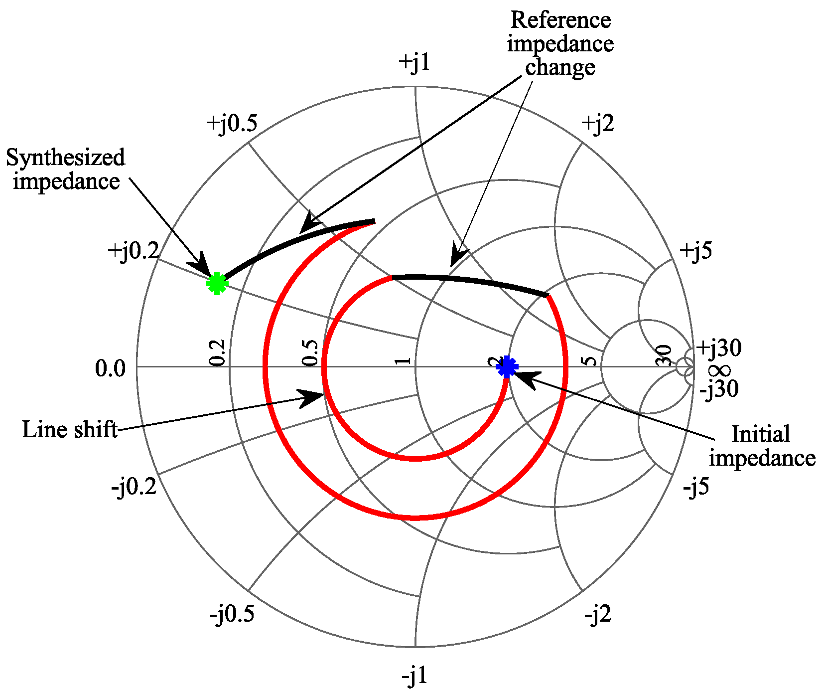
2.1. Design of the Impedance Synthesis Network

A DRW can be seen as equivalent to a transmission line whose RF response depends on the structure dimensions. As characteristic impedance ( Z 0 ) changes upon the width or the substrate height of a transmission line, so it does on a DRW, depending on the width and height of the ridge.
There are different ways in which the characteristic impedance can be defined. Among these are the voltage–current ( Z v i ), power–voltage ( Z p v ) and power–current ( Z p i ) definitions. While, for transmission lines, every definition provides the same result, that is not the case for an RWG, and neither is it for a DRW. For this study, Z p v has been used in every design process related to the DRW because it is the one that best fits the wave impedance ( Z T E ) when the fundamental mode is propagating [10].
For this work, designs of the impedance synthesis network were based on a stepped-ridge waveguide, following the concept of the stepped-impedance line transformer, a cascaded transmission lines circuit used for impedance-matching purposes but that again does not tackle the impedance synthesis. It is analyzed in [11]. Figure 2 shows the main idea of this paper, which is to take a cascaded transmission line as a generic model for a stepped-ridge DRW. Nonetheless, the model in Figure 2 is quite a simple one, and the discontinuity between two ridges with different heights needs to be analyzed.

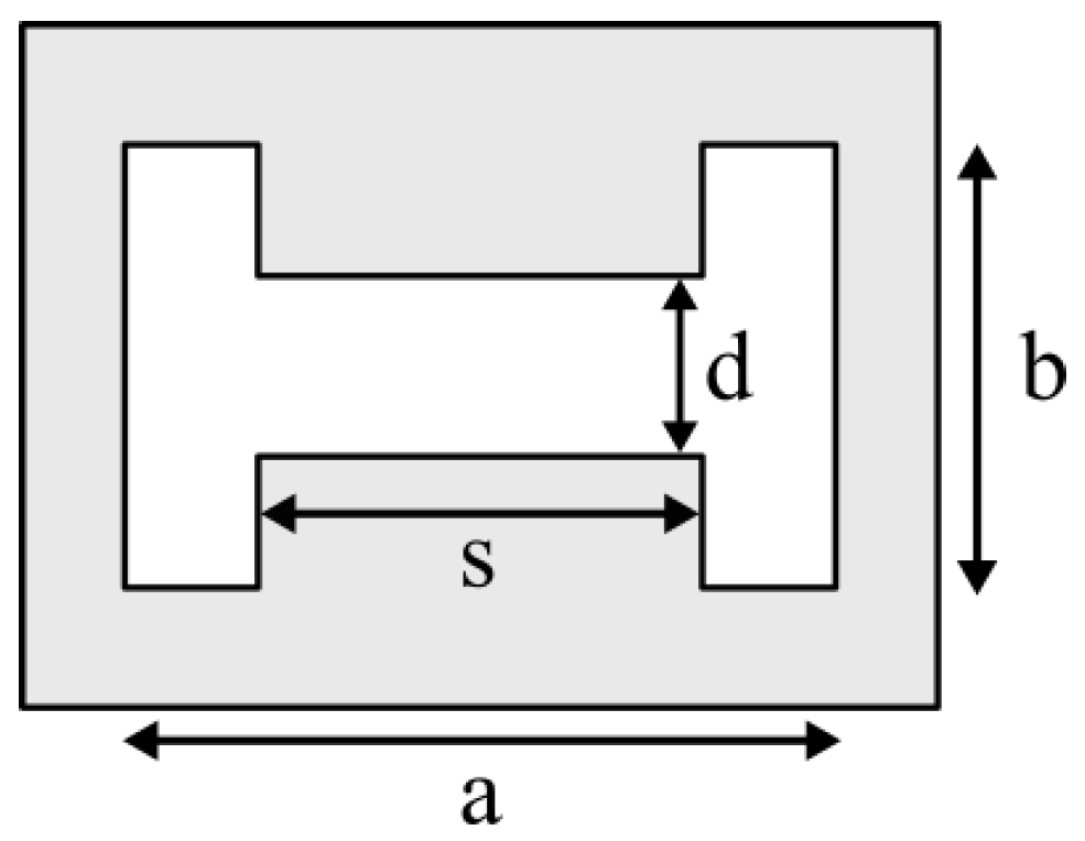
2.2. Ridge Discontinuity Analysis

The stepped-impedance RW is studied in [12]. The discontinuity between ridges is modeled, in this case, by a circuit made up of two transmission lines that introduce an extra delay and a reactive element placed parallel to the junction between the transmission lines. However, another alternative circuit presents a better option in terms of simulation analysis. It is shown in Figure 3. It is based on modeling the discontinuity using a three-lumped-element T-circuit.
For the case of the three-lumped elements circuit, a parametric S-parameter simulation of a DRW has been performed for different steps. Taking a DRW made of only two ridges and de-embedding the solution to the junction provides a response for the discontinuity. Figure 4 shows the structure upon which the parametric simulation has been carried out, where h s t e p ranges between 0.1 and 1.4 mm with a 0.1 mm step.
Once the simulations results showed in Figure 5 were obtained, results for each one of the three impedances in the model were extracted, as presented in Figure 6.
The discontinuity between the ridges is not expected to introduce losses; this is why the three impedances in Figure 6 are purely imaginary, with Z 1 and Z 2 exhibiting inductive behavior, while Z 3 is capacitive. Each impedance approaches 0 Ω as h s t e p increases, causing both the upper and lower ridges to be in near physical contact, which would result in a short circuit. Through simulation, it is finally checked that the modeled circuit response fits with that of the ridge discontinuity.

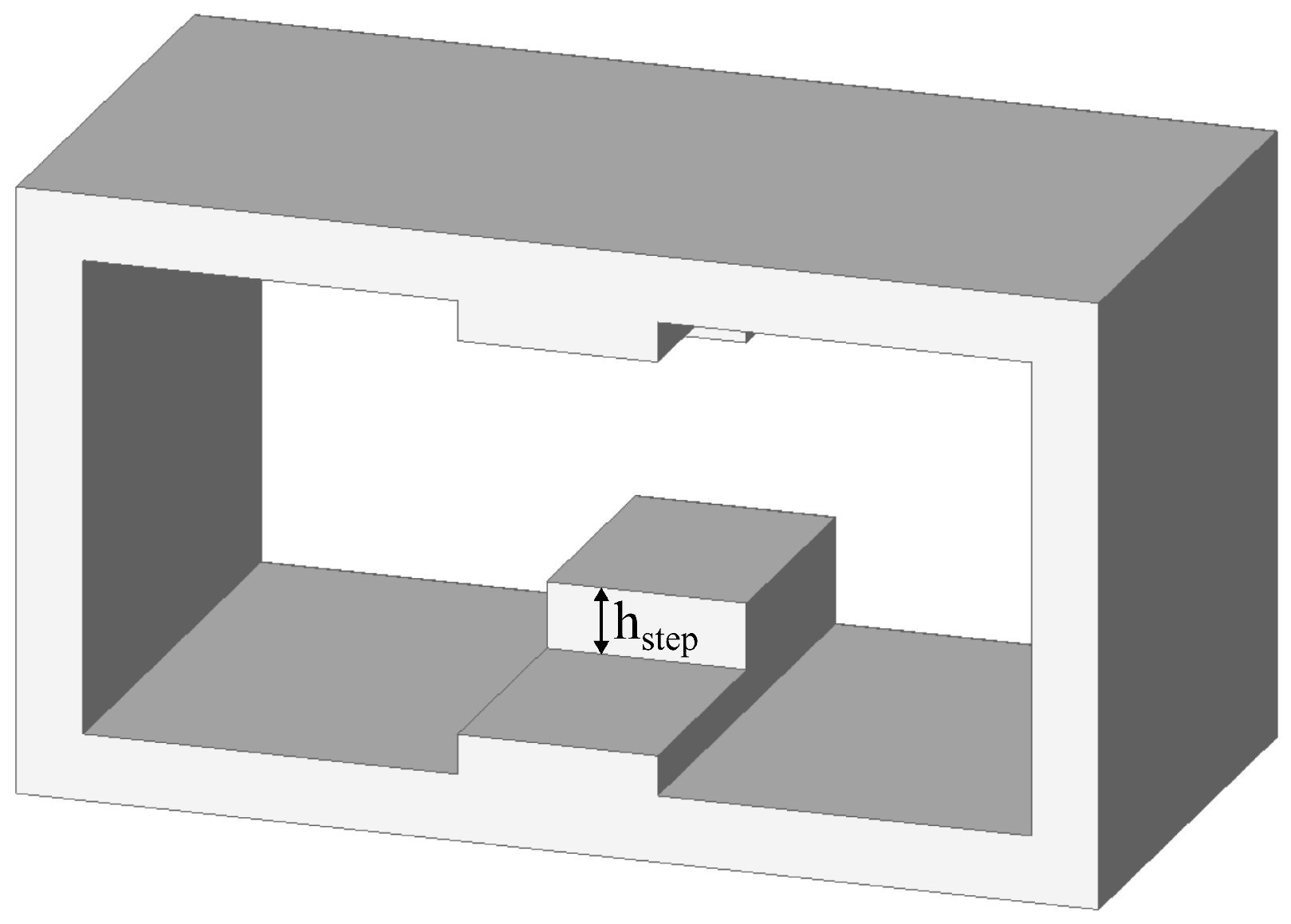
2.3. Analysis of a Single DRW
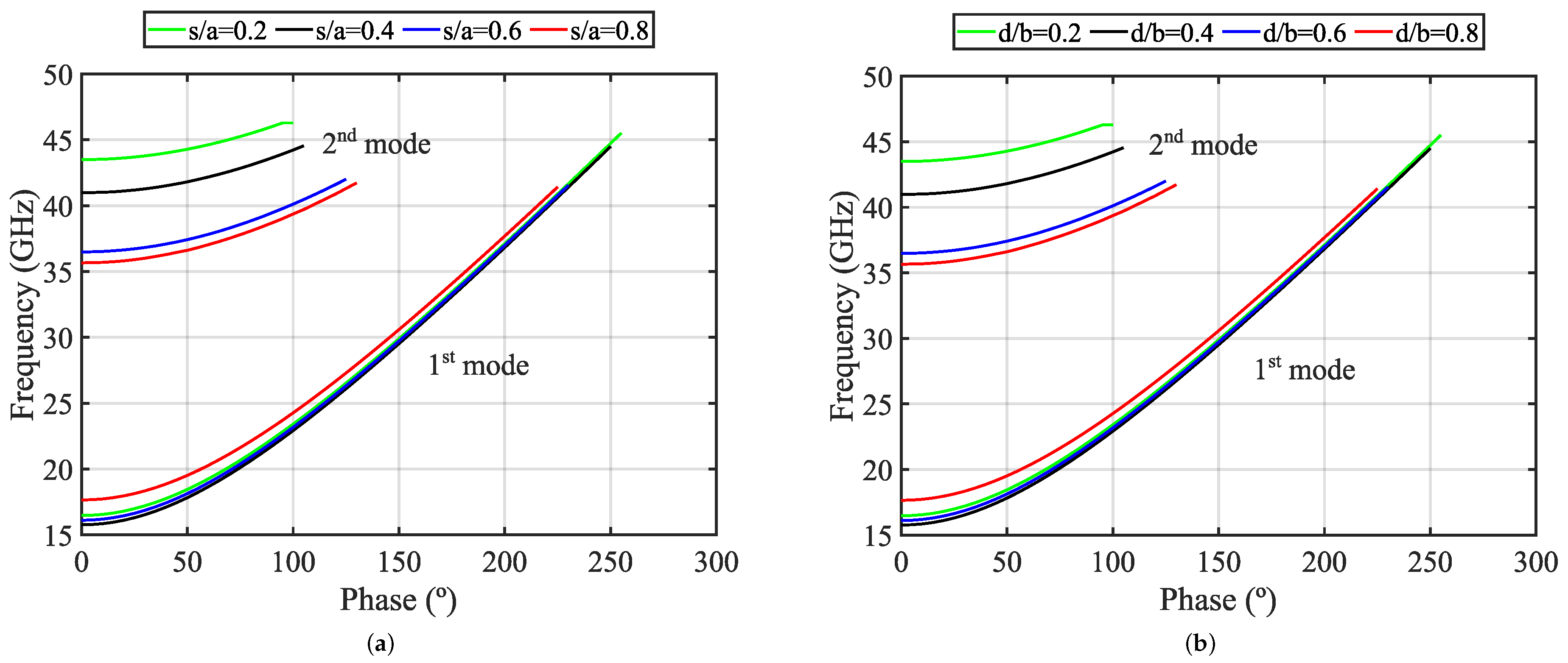
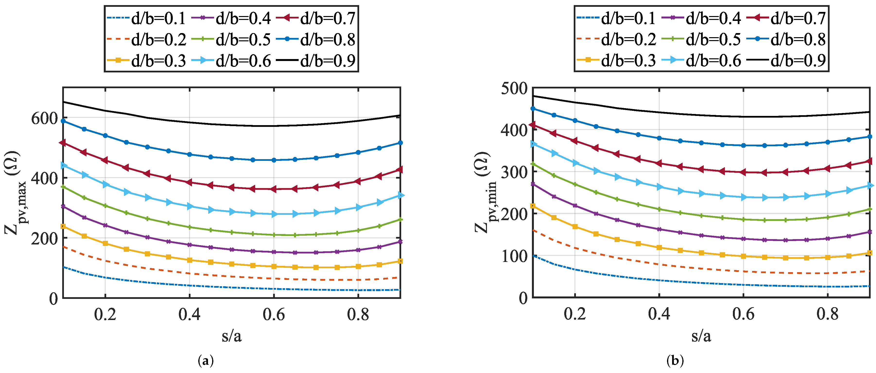
The design of the impedance synthesis network is based on a DRW changing its characteristic impedance along the ridge by making n steps of that ridge. Characteristic impedance of a ridge mainly depends on its width and height, which is why, prior to the design of a synthesis network, that relation must be studied.
Firs of all, some considerations must be taken into account. Physical properties of the DRW impose the first restriction in the design: neither ridge width nor height values can be higher than those of the RWG upon which the ridge is mounted.
Second, it is important to study the ridge frequency response, as this can impose another design restriction. Using an eigensolver from HFSS, a parametric eigenmode simulation was performed to obtain the dispersion diagram of a DRW for different combinations of its ridge width and height. Figure 7a,b show the results for four different combinations of width and height, respectively, with both parameters normalized to the RWG dimensions a and b.
From these results, it can be concluded that placing a metallic ridge inside an RWG leads to an increase of its cutoff frequency, more relevant in the case of the second mode. This is going to lead to the enhanced bandwidth that DRWs present in comparison to RWGs. Figure 8 shows the DRW bandwidth, considering monomode operation, for each one of the studied combinations. It can be seen how the bandwidth increases as the ridge becomes higher (lower values of d / b ) and reaches its optimum normalized width ( s / a ).
The impedance synthesis network requires reaching some particular and different characteristic impedance values on every ridge step along the DRW. Nonetheless, not every impedance is possible to be obtained. Figure 9a,b represent the maximum and minimum Z p v , respectively, depending on the ridge-normalized width and height in the operation frequency range, which is between 25 and 32 GHz.
Taking into account the combinations of height and width studied and according to Figure 9a,b, a range between 27 and 650 Ω for Z p v , approximately, could be covered only by changing the dimensions of the ridge.
A stepped-ridge waveguide causes an impedance transformation from one ridge to another. Therefore, the transition between different impedance paths can be analyzed not only through simulation but also through equations. Taking a two-transmission-line circuit, like the one in Figure 10, as a model for a two-ridge DRW and considering the interface between two reference planes, given by the characteristic impedance of each line, Z 01 and Z 02 , the impedance seen at the interface can be equally expressed as in (1). Both ρ 1 and ρ 2 are the reflection coefficients at the interface; they have the same direction and represent the same impedance value, but the difference between them is that each one refers to a different characteristic impedance, in this case, Z 01 and Z 02 , respectively.
Z 01 1 + ρ 1 1 ρ 1 = Z 02 1 + ρ 2 1 ρ 2
Operating with (1), the equivalence in (2) is obtained. Finally, isolating ρ 2 , the relation in (3) can be extracted, which determines the reflection coefficient associated to the synthesized impedance, being ρ 1 the reflection coefficient referenced to Z 01 line and ρ 2 the reflection coefficient referenced to Z 02 .
By analyzing the expression in (3), it can be deduced what the effect of the impedance reference change is and therefore what the possible impedance range is that this circuit can synthesize. It is concluded that any impedance can be synthesized, except those located on the edge of the Smith chart (i.e., ρ 2 = 1 ), because they will require one of these two conditions: Z 02 = 0 or ρ 1 = 1 , none of which is realizable on a DRW structure. Then, it can be concluded that by using this impedance synthesis technique, any impedance could be generated, except pure imaginary values. Nonetheless, previously explained restrictions should also be taken into consideration.
Z 01 ( 1 + ρ 1 ) ( 1 ρ 2 ) = Z 02 ( 1 + ρ 2 ) ( 1 ρ 1 )
ρ 2 = Z 01 ( 1 + ρ 1 ) Z 02 ( 1 ρ 1 ) Z 01 ( 1 + ρ 1 ) + Z 02 ( 1 ρ 1 )
Figure 11 illustrates the transformation from a constant-modulus-reflection-coefficient circle located at the center of the Smith chart to other two circles, which is caused by the change in the characteristic impedance, which is the reference impedance, in the next line or ridge. The black circle at the center is associated with the Z 01 reference. Going from this impedance to a two-times higher or two-times lower value of Z 02 will cause it to move to the left or right circle, respectively. Therefore, multiple circles can be generated, while the chosen Z 0 for the ridge is one of the restricted Z p v values in Figure 9a,b. These circles are defined by their center X 0 and radius r, and their equations in (4) and (5) are derived by performing a bilinear transformation between ρ 1 and ρ 2 and can be calculated as follows:
X 0 = | ρ 1 | 2 ρ Z * ρ Z | ρ 1 | 2 | ρ Z | 2 1
r = X 0 2 | ρ 1 | 2 | ρ Z | 2 | ρ 1 | 2 | ρ Z | 2 1
ρ Z = Z 01 Z 02 Z 01 + Z 02
where ρ Z is the reflection coefficient between the two reference planes calculated in (6).
Taking into consideration the length of every ridge as well as the characteristic impedance change, numerous movements could be realized in the Smith chart until the target impedance is found, following a path like in Figure 12. Once it is reached, values for electrical length and Z 0 of every ridge can be extracted from the Smith chart. Physical length is calculated from the electrical length and taking into account that the propagation constant for every ridge is different and depends on its physical properties. The Z 0 of every ridge will establish its width and height according to Figure 9a,b.

3. Results

Two different impedance synthesis networks were designed in order to demonstrate the ability of the DRW to synthesize different impedance values at a central frequency of 28 GHz: one with a reflection coefficient around center of the Smith chart and a more distant impedance value located near the edge of the Smith chart.
Figure 13 shows the design for the DRW synthesis networks. They were manufactured on aluminum WR28 RWG using the binder-jetting technique. A microstrip line, mounted on 20 mils of Rogers R04003C, was also used to facilitate the measurement, using a 2.92 mm (K) 50 Ω RF coaxial connector. The transition from the DRW to the 50 Ω microstrip line was made through contact between the top and bottom ridges and both metallic layers of the microstrip line. The dimensions for the two designs are shown in Table 1. Additionally, an equivalent ideal-transmission line model of the impedance synthesis network has been included in Figure 14. This model consists of a WR28 load located at the input, which represents the WR28 RWG port of the network and also presents three T-circuits in every discontinuity, corresponding to both the transitions between ridges and from the ridge waveguide to the WR28 port. Its dimensions are presented in Table 2.
The setup in Figure 13c was arranged to measure the frequency response of each one of the synthesized impedances between 26.5 and 35 GHz. A WR28 waveguide load was placed on the waveguide port, while connection to the PNA-X was made through the microstrip line. A 1-port microstrip calibration was carried out in the PNA-X using three home-made open circuit standards, corresponding to an offset of 0, λ/8 and λ/4. Figure 15 shows a comparison between the measured and simulated reflection coefficient for each one of the synthesis networks.
The results show that a good match is obtained for the two synthesized impedances. Little difference between measurements and simulation results are due to the manufacturing tolerance, which, in this case, was about 50 μm. It is important to consider that fabrication precision can really affect the performance of the impedance synthesis network because a different dimension of only one of the ridges, for instance, could result in having another characteristic impedance for that part of the taper and then a different synthesized impedance. Even more, if the height of the third ridge is not correct, this could affect the transition between the ridge and the microstrip circuit.

4. Discussion

In this work, a new way to synthesize impedances based on a DRW was presented. It has been shown that most of the impedances in the Smith chart can be synthesized, with some restrictions outlined in Section 2, such as the physical dimensions of the RWG upon which the double-ridge is mounted, as well as the limitations in terms of operating frequency and those derived from the mathematical analysis of the discontinuity between two different ridges. Two impedance synthesis networks were manufactured and measured to test their performance. A good match between the measurements and simulated results was obtained, proving that it is possible to use a DRW as an impedance synthesis network.
Therefore, from the study in this paper, it can be concluded that an impedance synthesis network based on DRWs can be an effective method to integrate RF amplifiers with waveguide technology in order to make this component more efficient in terms of losses. It has been proven that DRWs can operate as impedance synthesis networks; future studies should tackle, among other things, the viability of that integration.

Author Contributions

Methodology, J.J.F.R.; Software, J.J.F.R.; Validation, L.F.H.; Formal analysis, J.J.F.R. and L.F.H.; Investigation, J.J.F.R.; Writing—original draft, J.J.F.R.; Writing—review & editing, L.F.H.; Supervision, L.F.H. All authors have read and agreed to the published version of the manuscript.

Funding

This work has been funded by Gobierno del Principado de Asturias under “Severo Ochoa” Program Grant PA-23-BP22-105 and the Government of Asturias-Sekuens/FEDER under grant IDE-2024-000693.

Data Availability Statement

The original contributions presented in this study are included in the article. Further inquiries can be directed to the corresponding author.

Conflicts of Interest

The authors declare no conflicts of interest. The funders had no role in the design of the study; in the collection, analyses, or interpretation of data; in the writing of the manuscript; or in the decision to publish the results.

Abbreviations

The following abbreviations are used in this manuscript:
DRWDouble-ridge waveguide
RWGRectangular waveguide
RWRidge waveguide
SIWSubstrate-integrated waveguide
SRWSingle-ridge waveguide

References

  1. Taryana, Y.; Sulaeman, Y.; Wahyu, Y.; Armi, N.; Paramayudha, K.; Rojak, R.A. Design of two stage low noise amplifier using double stub matching network. In Proceedings of the 2015 IEEE International Conference on Aerospace Electronics and Remote Sensing Technology (ICARES), Bali, Indonesia, 3–5 December 2015; pp. 1–5. [Google Scholar] [CrossRef]
  2. Thian, M. High-Efficiency Wilkinson-Power-Combining Class-EF Amplifier with Lumped-Element Load Network. In Proceedings of the 2018 IEEE Asia Pacific Conference on Circuits and Systems (APCCAS), Chengdu, China, 26–30 October 2018; pp. 199–202. [Google Scholar] [CrossRef]
  3. Hoefer, W.; Burton, M. Closed-Form Expressions for the Parameters of Finned and Ridged Waveguides. IEEE Trans. Microw. Theory Tech. 1982, 30, 2190–2194. [Google Scholar] [CrossRef]
  4. Moreira, J.; Churkin, S.; Hesselbarth, J. A Double-Ridged Waveguide Design for 5G mmWave Applications. In Proceedings of the 2022 Asia-Pacific Microwave Conference (APMC), Yokohama, Japan, 29 November–2 December 2022; pp. 824–826. [Google Scholar] [CrossRef]
  5. Michailidis, A.; Noulis, T. Algorithm-based Wide-Band Impedance Matching Network Synthesis and Optimization. In Proceedings of the 2024 20th International Conference on Synthesis, Modeling, Analysis and Simulation Methods and Applications to Circuit Design (SMACD), Volos, Greece, 2–5 July 2024; pp. 1–4. [Google Scholar] [CrossRef]
  6. Uz Zaman, A.; Vukusic, T.; Alexanderson, M.; Kildal, P.S. Design of a Simple Transition From Microstrip to Ridge Gap Waveguide Suited for MMIC and Antenna Integration. IEEE Antennas Wirel. Propag. Lett. 2013, 12, 1558–1561. [Google Scholar] [CrossRef]
  7. Vilenskiy, A.R.; Zhang, Y. A Compact and Wideband MMIC-to-Ridge Gap Waveguide Contactless Transition for Phased Array Antenna Front Ends. IEEE Antennas Wirel. Propag. Lett. 2024, 23, 990–994. [Google Scholar] [CrossRef]
  8. Cano, J.L.; Mediavilla, A.; Perez, A.R. Full-Band Air-Filled Waveguide-to-Substrate Integrated Waveguide (SIW) Direct Transition. IEEE Microw. Wirel. Components Lett. 2015, 25, 79–81. [Google Scholar] [CrossRef]
  9. Shi, X.; Xue, Y.; Yang, Y.J.; Chen, J.X. A Wideband DRWG Balun With Low Loss and Compact Size. IEEE Microw. Wirel. Technol. Lett. 2024, 34, 379–382. [Google Scholar] [CrossRef]
  10. Helszajn, J. Ridge Waveguides and Passive Microwave Components; The Institution of Engineering and Technology: London, UK, 2000. [Google Scholar]
  11. Steer, M. Microwave and RF Design: Networks, Volume 3; NC State University: Raleigh, NC, USA, 2019. [Google Scholar]
  12. Yao, H.W.; Abdelmonem, A.; Liang, J.F.; Zaki, K. Analysis and Design of Microstrip-to-Wavguide Transitions. IEEE Trans. Microw. Theory Tech. 1994, 42, 2371–2380. [Google Scholar] [CrossRef]
Figure 1. Front section of a double-ridge waveguide (DRW) with its main parameters.
Electronics 14 01060 g001
Figure 2. Generic model equivalence between the profile section of a DRW with n step variations (bottom) and a circuit made of an n transmission lines cascade (top).
Electronics 14 01060 g002
Figure 3. Ridge discontinuity model based on a three−lumped elements T−circuit.
Electronics 14 01060 g003
Figure 4. Step in the junction between two ridges.
Electronics 14 01060 g004
Figure 5. S-parameter simulation results for the DRW discontinuity.
Electronics 14 01060 g005
Figure 6. Extracted impedance results for the T-circuit model: (a) Imaginary part of Z 1 . (b) Imaginary part of Z 2 . (c) Imaginary part of Z 3 .
Electronics 14 01060 g006
Figure 7. Dispersion diagrams obtained from a parametric simulation: (a) Sweep of s / a ( d / b = 0.5 ). (b) Sweep of d / b ( s / a = 0.5 ).
Electronics 14 01060 g007
Figure 8. Analysis of operation bandwidth of a DRW for different combinations of s and d.
Electronics 14 01060 g008
Figure 9. Ridge impedance analysis: (a) Maximum Z p v possible values of a DRW for different combinations of s and d between 25 and 32 GHz. (b) Minimum Z p v possible values of a DRW for different combinations of s and d between 25 and 32 GHz.
Electronics 14 01060 g009
Figure 10. Transmission lines model of a two-ridge DRW.
Electronics 14 01060 g010
Figure 11. Constant-reflection coefficient circle transformation by change on the reference impedance.
Electronics 14 01060 g011
Figure 12. Synthesis of an arbitrary impedance in the Smith chart.
Electronics 14 01060 g012
Figure 13. Manufactured impedance synthesis networks: (a) Near-center-located impedance. (b) Near-edge-located impedance. (c) Impedance synthesis network measurement setup.
Electronics 14 01060 g013
Figure 14. Equivalent ideal model circuit.
Electronics 14 01060 g014
Figure 15. Simulated and measured results of reflection coefficient: (a) Near-center-located impedance. (b) Near-edge-located impedance.
Electronics 14 01060 g015
Table 1. Dimensions for the impedance synthesis networks.
d
(mm)
s
(mm)
Length
(mm)
Electrical
Length (°)
Z pv (Ω)
Center-
located
impedance
First Ridge2.6161.53.486.4424.3
Second Ridge1.8961.52.9579.2301
Third Ridge0.5441.54.6814493.4
Edge-
located
impedance
First Ridge1.5561.54.8133.2244
Second Ridge2.5561.5375.6413
Third Ridge0.5441.53.2100.893.4
Table 2. Parameters of the equivalent ideal model circuit.
Electrical
Length 1
(EL1) (°)
Electrical
Length 2
(EL2) (°)
Electrical
Length 3
(EL3) (°)
Z 01 (Ω) Z 02 (Ω) Z 03 (Ω) Z 1 _ 01 (Ω) Z 2 _ 01 (Ω) Z 3 _ 01 (Ω) Z 1 _ 12 (Ω) Z 2 _ 12 (Ω) Z 3 _ 12 (Ω) Z 1 _ 23 (Ω) Z 2 _ 23 (Ω) Z 3 _ 23 (Ω)
Center-
located
impedance
86.479.2144424.330193.44552.4 j4597.2 j−2310.8 j428.3 j449.2 j−329.8 j206.4 j203.7 j−123.3 j
Edge-
located
impedance
133.275.6100.824441393.4−1215.8 j−1242.1 j6300.5 j505.9 j544 j−429.6 j227.7 j236.9 j−133.6 j
Disclaimer/Publisher’s Note: The statements, opinions and data contained in all publications are solely those of the individual author(s) and contributor(s) and not of MDPI and/or the editor(s). MDPI and/or the editor(s) disclaim responsibility for any injury to people or property resulting from any ideas, methods, instructions or products referred to in the content.

