Abstract
This work develops a novel compact Silicon-Controlled Rectifier (SCR) model incorporating self-heating effects, extending the conventional Ebers–Moll (E–M) framework for Bipolar Junction Transistors (BJTs) by comprehensively integrating parasitic effects. The temperature dependence of critical device parameters, including junction capacitances, emitter resistances, and saturation currents, is systematically characterized to accurately predict the device’s electrical behavior under Electrostatic Discharge (ESD) stress. Furthermore, a self-heating modeling approach is introduced based on the SCR layout characteristics. The impact of self-heating on SCR transient response was verified by comparing simulation results with measurements from SCR devices fabricated in a 0.18 µm Bipolar-CMOS-DMOS (BCD) process. Comparative analysis demonstrates superior accuracy over existing models. The proposed SCR model includes a complete definition of parameters and electrical relationships, ensuring compatibility with various Electronic Design Automation (EDA) platforms.
1. Introduction
Owing to the high fabrication and measurement cost of the Integrated Circuits (ICs), the design and simulation of ICs’ electrical performance are becoming increasingly important in reducing the development time and cost. Simulation Program with Integrated Circuit Emphasis (SPICE) models are well established for conventional IC simulation, while system-level simulation that includes Electrostatic Discharge (ESD) protection devices has not been fully developed. Traditional ESD protection structures, including Bipolar Junction Transistors (BJTs), Gate-Grounded N-type MOS (GGNMOS), and diodes, are commonly modeled using standard model libraries provided by a foundry. These models provide accurate results for low-current operations but fail to represent the complex behaviors under ESD stress. With the quick development of the ICs’ fabrication process and electrical performance, those conventional ESD protection devices cannot meet the requirements of advanced ICs, due to the large area and weak ESD robustness. The Silicon-Controlled Rectifier (SCR) shows significant potential as an alternative ESD protection structure, due to its superior ESD robustness and area efficiency [1,2,3].
The SCR comprised coupled PNP and NPN BJTs in electrical characteristics; the electrical models of SCR suited for evaluating the large current discharge behavior resulted from the avalanche effect. Several SCR modeling approaches have been reported in the literature. An improved compact model compatible with industry-standard SPICE was proposed [4], but lacked comprehensive system-level simulation capabilities. A scalable SCR compact model [5] considered layout spacing and self-heating effects, but simulations of its snapback characteristics showed limited accuracy. The exist SCR models, including the parameter-efficient CMOS-SCR compact model [6] and the simplified physics-based model [7], have addressed simulation accuracy and convergence issues, respectively. However they fail to accurately capture the electrical performance variations caused by self-heating effects under ESD stress [8].
Despite attempts to incorporate complex physical models for parasitic effects, temperature-dependent variations in key device parameters (turn-on resistance, junction capacitance, and leakage current) remain for a challenge to modeling SCR device accurately. Although chip-level electro-thermal simulators that construct detailed 3D thermal networks can effectively analyze temperature profiles and hot spots, this approach involves extensive integration calculations [9,10]. These calculations impose unnecessary burdens for self-heating analysis of single-device ESD protection circuits and may introduce convergence issues in simulations. Such modeling methods are more suited for VLSI chip evaluations than for device-level ESD protection circuits. In some power device modeling studies, the impact of both environmental and internal device temperatures on heat dissipation efficiency has been considered [11,12,13]. This enhances the model’s accuracy in characterizing temperature variations within the device. However, these models lack an analysis of temperature-dependent parasitic parameters, making the influence of self-heating effects on the device’s electrical characteristics less apparent. Using a Cauer ladder thermal equivalent circuit to represent the temperature variations caused by self-heating effects within ESD protection devices has proven to be a viable approach [14,15]. However, further research is needed on the extraction of thermal capacitance and resistance of SCR devices, as well as how to effectively characterize the impact of self-heating on the electrical characteristics of SCRs. Using Technology Computer-Aided Design (TCAD) simulations to analyze the electrical characteristics of ESD protection devices has proven to be an excellent approach [16,17,18], yielding remarkable results. This method provides new insights and feasible strategies for further investigating the physical behaviors of ESD protection devices.
To more accurately describe the impact of self-heating effects on the electrical performance of SCRs and better predict their behavior under ESD stress, a compact SCR model incorporating self-heating effects is proposed. This model is based on a Cauer ladder thermal equivalent circuit, with thermal capacitance and thermal resistance parameters extracted from the SCR’s layout based on TCAD simulation results. It precisely simulates the lattice temperature variations caused by self-heating in the SCR, and temperature-sensitive physical parameters—including emitter resistance, junction capacitance, and reverse saturation current—are represented as functions of temperature to characterize the impact of self-heating on SCR electrical properties. This approach addresses the absence of proprietary self-heating models for SCR devices in earlier studies. Furthermore, the model is achieved using Verilog-A hardware description language, describing the coupling between SCR self-heating and electrical effects through loop algorithms. The simulation results obtained from SPICE demonstrate good agreement with experimental measurements, verifying the model’s accuracy in predicting the electrical characteristics of SCR devices.
2. Model Description
2.1. Silicon-Controlled Rectifier (SCR) Compact Model
Traditional SCR models feature a pair of mutually coupled transistors ( and ) and two linear well resistors ( and ) that provide bias to represent the equivalent circuit characteristics, as depicted in Figure 1. Although this simplified model is applicable under small-signal conditions, it fails to accurately capture the complex physical behaviors of the SCR under actual operating conditions. Especially when under ESD stress, the traditional SCR models (such as Ebers–Moll (E–M) and Gummel–Poon (G–P) models) are inadequate in reflecting nonlinear properties, including avalanche effects in the N-well/P-well regions and self-heating effects. The Vertical Bipolar Inter-Company (VBIC) transistor model can provide relevant nonlinear analysis but focuses on the I–V characteristics of individual transistors, making it unsuitable for describing the complex electro-thermal coupling within the SCR.
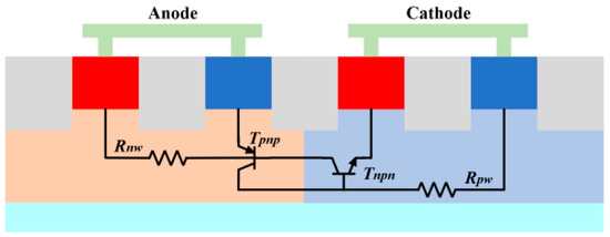
Figure 1.
Cross-sectional view and typical equivalent circuit diagrams of Silicon-Controlled Rectifier (SCR) structure.
Based on the aforementioned analysis, an improved transistor E–M model is proposed to describe SCR devices. As illustrated in Figure 2, the model introduces forward diodes , , and reverse diode , along with voltage-controlled current sources and , forming a typical transistor EM coupled current transmission model. In addition, an avalanche current source is used to describe the avalanche breakdown characteristics at the N-well/P-well reverse-biased junction when the electric field intensity reaches a critical value. Nonlinear resistances , , and are introduced to characterize the conductivity modulation and self-heating effects induced by large current injection under ESD stress. Moreover, the model includes parasitic capacitance modeling, which significantly impacts the SCR’s transient response. For the forward-biased p-n junctions at P+/N-well and P-well/N+, only the dominant diffusion capacitances and , are considered. For the reverse-biased N-well/P-well junction, the parasitic capacitance is represented by the diffusion capacitance and the junction capacitance .
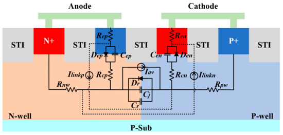
Figure 2.
Cross-sectional view of the SCR and the equivalent circuit diagram of the improved SCR model based on the Ebers–Moll (E–M) model.
The currents flowing through the forward diode , the reverse diode , and the voltage-controlled current source are given by Equations (1)–(3), as follows [5]:
where is the reverse saturation current, is the thermal voltage, and and are the forward and reverse gains of the transistor, respectively, which are taken as constants. and are the voltage drops across the forward diode and the reverse diode , respectively. The equations for the diode and the voltage-controlled current source are similar to those for and , respectively.
The avalanche current source is modeled using a piecewise function. When the voltage is lower than the critical breakdown voltage, the avalanche current is described by the equation shown in Equation (4). When the voltage exceeds the critical breakdown voltage, a linear equation, as shown in Equation (5), is used to avoid convergence issues [7,19].
where is the critical breakdown voltage, is a constant related to the physical properties of semiconductor material, the value of is close to 1 to ensure that breakdown occurs near the threshold, and is the differential resistance near the breakdown voltage.
The expression for the collector resistance is given by Equation (6), as shown below [7,20]:
where is the resistance value at zero bias, is the threshold charge, and is the number of charge injected into the N-well/P-well junction, which can be expressed by Equation (7):
where is the transit time of the N-well/P-well junction. The equation for the collector resistance is similar to that for .
The currents flowing through the diffusion capacitors and are given by Equations (8) and (9), as shown below [5]:
where and are the forward and reverse transit times, respectively. The equation for the diffusion capacitance is similar to that for .
In addition to the description of the electrical characteristics mentioned above, this study focused on the impact of self-heating effects on the electrical properties of SCRs. Under ESD stress, the power dissipation of the device causes an increase in lattice temperature, which triggers a series of temperature-dependent effects. This temperature dependence primarily manifests in the deviation of physical quantities, such as emitter resistance, junction capacitance, and reverse saturation current, from their initial values as temperature changes, significantly affecting the SCR’s electrical characteristics. Among these, the temperature dependence of the emitter resistance can be described by Equation (10) as follows [21,22]:
where represents the standard resistance value at room temperature, and is the temperature-dependent exponent. is the current temperature and is the initial temperature (ambient temperature), with values derived from the self-heating model. The equation for the emitter resistance is similar to that for . When increasing temperature, the enhanced carrier–lattice scattering in heavily doped emitter regions of SCR reduces carrier mobility, resulting in a super-linear growth in resistance. This nonlinear characteristic becomes particularly significant under high-current injection conditions, representing a critical physical phenomenon that conventional linear models fail to accurately describe.
The temperature dependence of junction capacitance involves complex physical mechanisms. The capacitance is primarily constrained by the width of the depletion region, and its temperature dependence can be expressed as follows [22]:
where represents the junction capacitance at room temperature, is the temperature coefficient, is a fitting parameter set to 4 × 10⁻⁴, and is the built-in potential, which is inversely proportional to temperature. is the initial built-in potential. The equation describes two fundamental mechanisms of how temperature affects the junction capacitance. As temperature increases, the intrinsic carrier concentration rises, enhancing the screening effect of the carriers on the electric field in the depletion region. Simultaneously, the increase in temperature reduces the semiconductor bandgap, thereby decreasing the built-in potential. Both effects lead to a narrowing of the depletion region, which in turn reduces the junction capacitance. The combined influence of these mechanisms determines the temperature-dependent behavior of the junction capacitance.
Apart from the effects on , , and , temperature significantly influences the reverse saturation current. When temperature increases, enhanced thermal generation enables more carriers to overcome the bandgap, intensifying the carrier generation-recombination processes. This temperature-dependent behavior can be expressed by the following equation [22,23]:
represents the temperature exponent factor, is the ideality factor, and denotes the bandgap width at room temperature. The equation accurately describes the mechanism by which temperature influences the reverse saturation current. Specifically, the term characterizes the variation in carrier concentration with temperature, while the exponential term reflects the impact of temperature on the carrier generation and recombination processes. This dual temperature dependence indicates that increased temperature substantially enhances carrier generation, resulting in strongly nonlinear characteristics of reverse saturation current.
The equation described above allows the model, as shown in Figure 2, to accurately capture the electro-thermal coupling within the SCR. This multi-physics coupling modeling approach significantly enhances the model’s accuracy under ESD stress conditions, demonstrating particular advantages in predicting device behavior under high-current injections. The parameters used in the compact model are listed in Table 1 for reference; all parameter values are obtained from relevant process manuals or fitted using tested results.

Table 1.
Reference values of parameters for the compact model.
2.2. SCR Self-Heating Model
Based on the previously described physical models, a self-heating model is developed to accurately characterize the impact of lattice temperature rise on SCR device characteristics. A novel self-heating modeling approach is proposed considering the specific SCR structure.
To precisely model the temperature distribution characteristics of SCR devices under ESD stress, 3D-TCAD simulations were conducted according to the SCR layout structure, as illustrated in Figure 3a. The SCR length is set to 8 µm, and the width is 100 µm (Since the device width is linearly proportional to the overcurrent capability, the width was scaled down by a factor of 10 during the simulation to improve computational speed, resulting in a simulated width of 10 µm). The diffusion depth of the lattice temperature is approximately 4 µm, and this portion is analyzed.
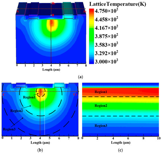
Figure 3.
The SCR’s response under a 1A transient pulse: (a) 3D-Technology Computer-Aided Design (TCAD) lattice temperature simulation; (b) cross-sectional profile along line A–A1; (c) cross-sectional profile along line B–B1.
Cross-sectional analyses were performed along the A–A1 and B–B1 directions depicted in Figure 3a. Figure 3b presents the temperature distribution profile along the A–A1 direction, clearly showing that the highest temperature region is located near the N-well/P-well junction, exhibiting distinct radial diffusion characteristics. This distribution pattern corresponds with the current concentration effect observed under ESD stress, reflecting the local hotspot phenomena induced by carrier injection. Figure 3c illustrates the temperature distribution along the B–B1 direction, revealing the lateral diffusion of heat. Based on the temperature gradient distribution characteristics, the SCR device is segmented into three distinct regions: Region 1, the central hotspot area with the highest temperature and steepest gradient; Region 2, the transitional area with moderate temperature and gradual gradient change; Region 3, the peripheral area with lower temperature approaching ambient conditions.
TCAD simulation results suggest that the heat dissipation region can be approximated as a semi-cylindrical space, as illustrated in Figure 4a. The region with radius corresponds to the highest temperature red hot spot (Region 1) in Figure 3b,c, followed by the region between and . The outermost region between and , represented by the blue area (Region 3), exhibits temperature values approaching the ambient temperature, forming a distinct temperature gradient with the high-temperature central region.
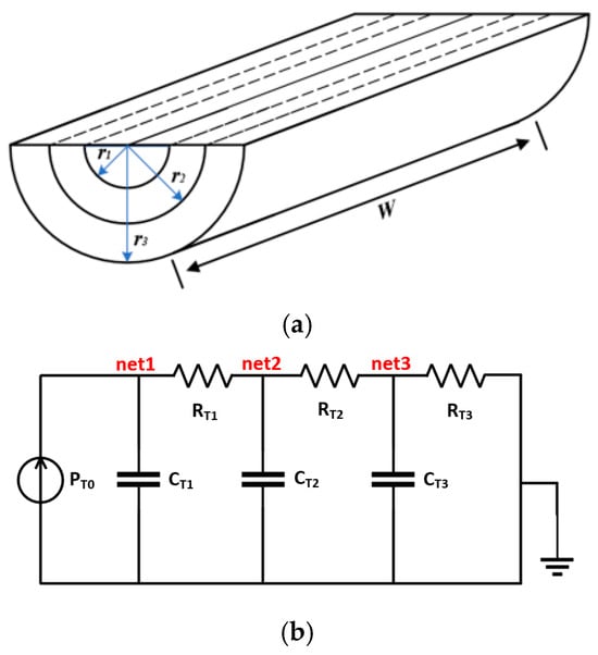
Figure 4.
The SCR’s: (a) Equivalent diagram of heat distribution; (b) equivalent circuit of the thermal network.
Based on the thermal conduction characteristics of each region, the thermal energy volume and heat dissipation efficiency of each region are described using thermal capacitance and thermal resistances . Here, and are modeled as fixed values that depend solely on the material and dimensions, neglecting the effects of dissipated power and internal temperature variations on heat dissipation efficiency. This simplification is made because the self-heating model is intended to provide a reference lattice temperature for the temperature-dependent parameters in the compact SCR model. The primary focus of the calculations is on the heat source temperature, and the nonlinear variations in heat dissipation efficiency, being small, have limited impact on the heat source temperature during thermal conduction. Additionally, since SCRs typically operate in low-frequency application, the changes in thermal accumulation during conduction are relatively gradual, and nonlinear effects do not significantly affect the overall thermal response. Therefore, by neglecting the nonlinear changes in heat dissipation efficiency, sufficient accuracy is maintained while avoiding the introduction of complex nonlinear calculations that could cause convergence issues, thus improving computational efficiency. The corresponding thermal resistance and thermal capacitance are represented by Equations (13)–(16) as shown below [24]:
Here, represents the thermal conductivity of silicon, which varies with temperature and doping concentration; denotes the effective width of the device; correspond to the characteristic radii of each region; is the silicon density; is the specific heat capacity of silicon. Both the and determines the heat transfer characteristics within the device. Table 2 lists the parameters of the above self-heating model for reference.
Table 2.
Reference values of parameters for the self-heating model.
Based on Equations (13)–(16), a SPICE-compatible equivalent circuit model is implemented using Cauer network topology, while retaining the physical heat conduction characteristics. As illustrated in Figure 4b, the thermal resistances and thermal capacitances of the temperature regions are converted into a series RC network. The excitation source originates from the transient output power of the SCR compact model and can be mapped as a current source in this thermal network. The node voltages net1, net2, and net3 correspond to temperature values that decrease progressively from the hot spot to the outer region. This layered RC structure not only reflects the spatial characteristics of heat transfer but also accurately describes the temperature coupling relationships between regions. The model provides reliable simulation of transient thermal response during ESD events, enabling accurate assessment of device thermodynamic behavior.
The self-heating model is tightly integrated with the previously described SCR physical model through a feedback loop, as depicted in Figure 5, thereby establishing a comprehensive temperature feedback system. Under ESD stress conditions, this coupling manifests as a dynamic feedback process. The ESD current generates Joule heating, leading to temperature rise, which modifies device parameters (such as mobility and depletion region width). These parameter variations alter the current distribution, resulting in new temperature profiles and forming a sustained positive feedback loop. Appropriate feedback mechanisms must be established in the model to account for these complex thermal-electrical coupling effects. The model presented in this study was developed using the hardware description language Verilog-A, enabling this feedback mechanism to be realized through a looping algorithm during programming.
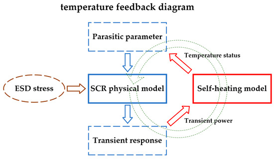
Figure 5.
Schematic diagram of temperature feedback in SCR model.
3. Model Verification
To verify the proposed self-heating model, SCR devices with a width of 100 μm were fabricated in a 0.18 μm Bipolar-CMOS-DMOS (BCD) process. 3D-TCAD simulations provided reference data by obtaining lattice temperature distributions across different device regions under ESD stress. The Direct Current (DC) turn-on characteristics were then measured using semiconductor parameter analyzer. A Transmission Line Pulse (TLP) system with 10 ns rise time and 100 ns pulse width was employed to evaluate the transient characteristics and quasi-static characteristics (V–T and I–V curves), enabling comprehensive assessment of self-heating effects on device performance.
3.1. Analysis of Self-Heating Effects in Compact Model
SPICE simulation was performed to analyze the transient thermal response of the proposed SCR model under ESD stress. A 1A current pulse with 100 ns duration was applied to the compact SCR model incorporating the self-heating effects. As shown in Figure 6, the temperature response curves of the three characteristic regions demonstrate rapid temperature rise at pulse onset followed by gradual decrease after ESD pulse, revealing the device’s thermal dynamic characteristics. The spatial temperature distribution shows a consistent decrease from Region 1 to Region 3, aligning with the physical heat diffusion process from center to periphery.
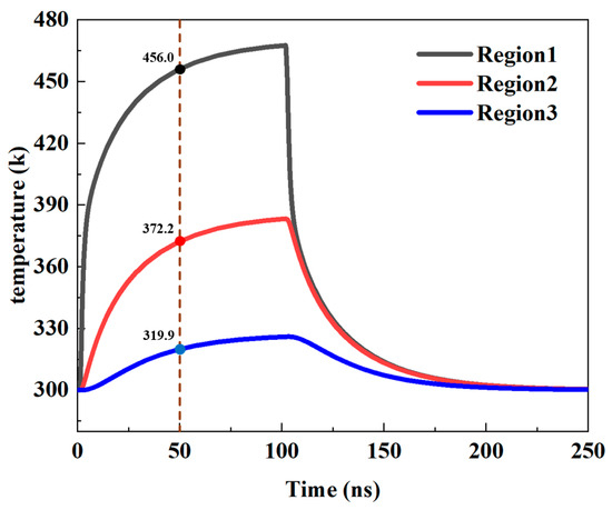
Figure 6.
Simulation Program with Integrated Circuit Emphasis (SPICE) simulation results of temperature variation over time in regions 1, 2, and 3 under a 1A current pulse.
To further validate the model accuracy, transient temperature distributions of the SCR device by stressing the 1A current pulse were analyzed using 3D-TCAD simulations. Figure 7 shows the lattice temperature distribution along line C–C1 in Figure 3b at t = 50 ns. The spatial regions in the self-heating model were divided into three zones (indicated by pink, green, and blue colors in Figure 7), and compared with SPICE simulation results at the same point in time. Despite using piecewise linear approximation, the proposed model predicts temperature distributions that closely match the continuous temperature field from TCAD simulations. The good agreement between temperature predictions in different regions demonstrates the model effectiveness.
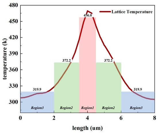
Figure 7.
Comparison of lattice temperature from TCAD simulation and SPICE model simulation at 50 ns under a 1A current pulse.
3.2. Analysis of Key Parameters in Compact Model
3.2.1. Emitter Resistance
The impact of emitter resistance self-heating on SCR compact model accuracy was evaluated by comparing simulations with and without the self-heating model under a 1A current pulse, as shown in Figure 8. During steady-state (70–90 ns), experimental measurements (black dotted lines) show a clamping voltage of 5.75 V. Simulations without self-heating (red curve) predict 4.98 V, yielding an 11% error due to neglecting temperature-dependent resistance increases. Including the self-heating model (blue curve) corrects the on-state resistance temperature dependence, resulting in a predicted clamping voltage of 5.77 V with approximately 1% error. The minor voltage fluctuations observed between 30–50 ns in the experimental curve originate from TLP measurement system reflections rather than intrinsic SCR characteristics and can be excluded from model considerations.
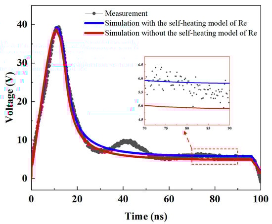
Figure 8.
Comparison of transient response (V–T curves) before and after incorporating the emitter resistance self-heating model.
3.2.2. Junction Capacitance
Similar to the emitter resistance analysis, the junction capacitance self-heating model was evaluated. Equation (17) was adopted for practical simulations due to the complexity of the built-in potential expression in Equation (11) and potential numerical convergence issues:
The junction capacitance primarily affects the overshoot voltage in SCR transient characteristics. Under a 1A current pulse (Figure 9), experimental measurements showed an overshoot voltage of 39.3 V. Simulations without the self-heating model predicted 41.5 V (5.6% error), as the underestimated capacitance reduced transient current suppression capabilities. Incorporating temperature-dependent junction capacitance corrected the overshoot voltage to 39.3 V, matching experimental results. This improvement is particularly significant for high-frequency applications where accurate overshoot voltage prediction is crucial for device protection assessment.
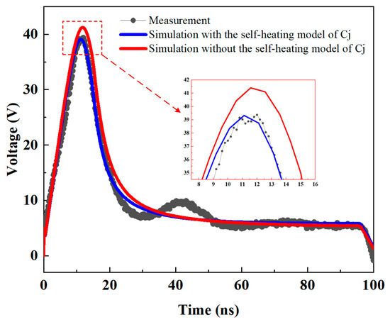
Figure 9.
Comparison of transient response (V–T curves) before and after incorporating the junction capacitance self-heating model.
3.2.3. Reverse Saturation Current
Temperature dependency of reverse saturation current significantly influences SCR device behavior. The exponential growth of reverse saturation current with temperature enhances carrier generation and internal electric field formation. This results in reduced trigger threshold voltage and accelerated post-trigger anode current increase. Consequently, the device exhibits faster overshoot voltage decay and improved conducting state stability.
A comparative analysis of transient response with and without temperature effects was performed under a 1A current pulse, as shown in Figure 10. Without temperature effects, the model predicted an overshoot voltage of 42.2 V compared to the measured 39.3 V. The discrepancy became more pronounced during voltage decay: at 25 ns post-pulse, the measured voltage decreased to 8.9 V, while the model without temperature effects showed 13.5 V. Including temperature effects on reverse saturation current improved the prediction accuracy significantly, with simulated voltage decreasing to 9.8 V. This enhancement demonstrates the critical role of temperature-dependent reverse saturation current in modeling transient conduction behavior for ESD protection applications.
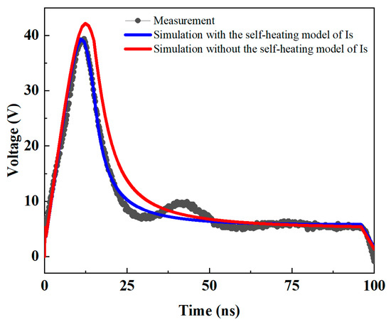
Figure 10.
Comparison of transient response (V–T curves) before and after incorporating the reverse saturation current self-heating model.
3.3. Analysis of the Direct Current (DC) and Quasi-Static Characteristics of Compact Model
DC characteristics were measured using a voltage source with 0.2 V steps and 1 mA current limit, as shown in Figure 11. The measured data (black dotted lines) show strong avalanche breakdown at the N-well/P-well junction when voltage reaches 14.2 V, causing the current to rise rapidly to the 1 mA limit. The device exhibits good off-state performance with a leakage current below 1 pA. The simulation results (red curve) accurately demonstrate both turn-on and turn-off characteristics, validating the model’s effectiveness.
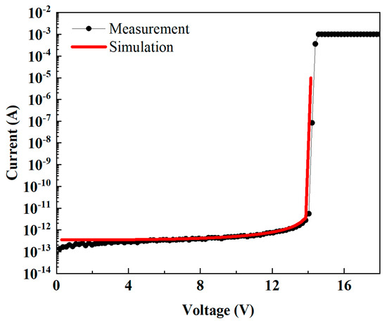
Figure 11.
Comparison of simulated and measured Direct Current (DC) characteristics.
It should be noted that, prior to SCR turn-on, the device’s leakage current is too small to cause a noticeable rise in lattice temperature, so the impact of self-heating effects on the DC response of the SCR is negligible. However, once the SCR is turned on, self-heating effects significantly influence the SCR’s quasi-static I–V characteristics.
The quasi-static I–V characteristics were validated using TLP measurements. The I–V curve was extracted by averaging voltage and current values within 70–90 ns window under various TLP pulses, as shown in Figure 12. The experimental results (black dotted lines) show a trigger voltage of 18.6 V, holding voltage of 4.5 V, and on-state resistance Ron of 1.9 Ω. The simulation results without self-heating effects (red curve) show a trigger voltage of 18.9 V, a holding voltage of 4.3 V, and an on-state resistance of 0.9 Ω. This error primarily stems from the temperature dependence of junction capacitance, reverse saturation current, and emitter resistance, which were detailed in Section 3.2. The most significant issue is the approximately halved on-state resistance, which can severely impact the model’s predictive accuracy. In contrast, the simulation results with self-heating effects (blue curve) demonstrate good agreement with measurements, validating the accuracy of the model in characterizing the SCR device’s behavior. These results establish a reliable basis for both ESD protection circuit design and SCR device optimization.
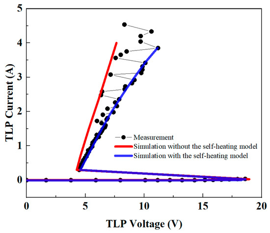
Figure 12.
Comparison of quasi-static I–V characteristics before and after incorporating the self-heating model.
4. Conclusions
This study proposes a compact SCR model incorporating self-heating effects. The model represents lattice temperature variations under ESD stress through a thermal network and describes temperature-dependent physical parameters within the SCR. Experimental validation demonstrates that the compact SCR model, with self-heating effects included, exhibits high accuracy in predicting both DC and transient responses, accurately characterizing the SCR’s turn-on and clamping behaviors. For circuit designers, this model provides a reliable choice for the design and optimization of ESD protection units. Furthermore, the model is implemented in Verilog-A, independent of predefined process model libraries. All parameters and circuit connections are defined within the code, enabling seamless integration with mainstream Electronic Design Automation (EDA) tools such as Advanced Design System (ADS) and Virtuoso, offering excellent portability and ease of use for circuit designers.
However, there are potential limitations in the application of this model under extreme conditions. To improve simulation convergence and computational efficiency, the model simplifies by neglecting nonlinear variations in heat dissipation efficiency during thermal conduction. This simplification has negligible effects on simulation results in typical ESD protection scenarios but may influence accuracy in high-frequency applications due to the repeated accumulation of heat. Future studies can address this issue by modeling thermal resistance as a function of temperature and dissipated power. Additionally, under extreme high-temperature conditions, the device’s thermal failure must be considered. The model can be extended to include critical temperature markers, providing investigators with timely feedback to prevent simulated current from exceeding the device’s limits.
Author Contributions
Conceptualization, methodology, validation, writing—original draft preparation, H.W. and H.L.; investigation, data curation, H.W.; writing—review and editing, J.L., H.L. and H.W.; funding acquisition, J.L. All authors have read and agreed to the published version of the manuscript.
Funding
This work is supported by the Joint Project of Yangtze River Delta Community of Sci-Tech Innovation (Grant No. 2022CSJGG0400), in part by the Natural Science Foundation of Jiangsu Province of China (Grant No. BK20231038), and in part by the Fundamental Research Funds for the Central Universities (Grant No. JUSRP123062).
Data Availability Statement
Data are contained within the article.
Conflicts of Interest
The authors declare no conflicts of interest.
Abbreviations
The following abbreviations are used in this manuscript:
| SCR | Silicon Controlled Rectifier |
| ESD | Electrostatic Discharge |
| ICs | Integrated Circuits |
| BJT | Bipolar Junction Transistors |
| GGNMOS | Gate-Grounded N-type MOS |
| EDA | Electronic Design Automation |
| E–M | Ebers–Moll |
| G–P | Gummel–Poon |
| VBIC | Vertical Bipolar Inter-Company |
| TCAD | Technology Computer Aided Design |
| SPICE | Simulation Program with Integrated Circuit Emphasis |
| BCD | Bipolar-CMOS-DMOS |
| TLP | Transmission Line Pulse |
| DC | Direct Current |
| ADS | Advanced Design System |
References
- Chen, Y.; Zhao, D.; Zhou, S.; Zhu, X.; Gao, F.; Yuan, Y.; Hu, Y.; Zhao, T.; Li, X.; Dong, S. High Area Efficiency Bidirectional Silicon-Controlled Rectifier for Low-Voltage Electrostatic Discharge Protection. Electronics 2023, 12, 4011. [Google Scholar] [CrossRef]
- Liang, H.; Cao, X.; Liu, J.; Sun, J.; Liang, H.; Xu, J.; Lei, W.; Gu, X. A Novel Dual-Direction SCR Embedded with Segmental and Cross-Bridge Topology for High-Voltage ESD Protection. IEEE Trans. Electron Devices 2023, 70, 4036–4042. [Google Scholar] [CrossRef]
- Kwon, S.-W.; Koo, Y.-S. Design of Capacitor-Less High Reliability LDO Regulator with LVTSCR Based ESD Protection Circuit Using Current Driving Buffer Structure. Electronics 2022, 11, 1781. [Google Scholar] [CrossRef]
- Cao, J.; Xu, J.; Wang, Y.; Lu, G.; Zhang, X. A Compact SCR Model Using Advanced BJT Models and Standard SPICE Elements. Sci. China Inf. Sci. 2016, 59, 109302. [Google Scholar] [CrossRef]
- Di Sarro, J.P.; Rosenbaum, E. A Scalable SCR Compact Model for ESD Circuit Simulation. IEEE Trans. Electron Devices 2010, 57, 3275–3286. [Google Scholar] [CrossRef]
- Mertens, R.; Rosenbaum, E. Physical Basis for CMOS SCR Compact Models. IEEE Trans. Electron Devices 2016, 63, 296–302. [Google Scholar] [CrossRef]
- Yan, X.; Mousavi, S.M.; Shen, L.; Xu, Y.; Zhang, W.; Bub, S.; Holland, S.; Beetner, D.G. A Physics-Based Model for Snapback-Type ESD Protection Devices. IEEE Trans. Electromagn. Compat. 2023, 65, 1273–1281. [Google Scholar] [CrossRef]
- Liang, W.; Dong, A.; Li, H.; Miao, M.; Kuo, C.-C.; Klebanov, M.; Liou, J.J. Characteristics of ESD Protection Devices Operated Under Elevated Temperatures. Microelectron. Reliab. 2016, 66, 46–51. [Google Scholar] [CrossRef]
- Cheng, Y.-K.; Raha, P.; Teng, C.-C.; Rosenbaum, E.; Kang, S.-M. ILLIADS-T: An Electrothermal Timing Simulator for Temperature-Sensitive Reliability Diagnosis of CMOS VLSI Chips. IEEE Trans. Comput. Aided Des. Integr. Circuits Syst. 1998, 17, 668–681. [Google Scholar] [CrossRef]
- Ma, X.; Xu, Q.; Wang, C.; Cao, H.; Liu, J.; Zhang, D.; Li, Z. An Electrical-Thermal Co-Simulation Model of Chiplet Heterogeneous Integration Systems. IEEE Trans. VLSI Syst. 2024, 32, 1769–1781. [Google Scholar] [CrossRef]
- Chang, Y.; Li, W.; Luo, H.; He, X.; Iannuzzo, F.; Blaabjerg, F.; Lin, W. A 3D Thermal Network Model for Monitoring Imbalanced Thermal Distribution of Press-Pack IGBT Modules in MMC-HVDC Applications. Energies 2019, 12, 1319. [Google Scholar] [CrossRef]
- Gorecki, K.; Gorecki, P.; Zarebski, J. Measurements of Parameters of the Thermal Model of the IGBT Module. IEEE Trans. Instrum. Meas. 2019, 68, 4864–4875. [Google Scholar] [CrossRef]
- Górecki, K.; Górecki, P. Nonlinear Compact Thermal Model of the IGBT Dedicated to SPICE. IEEE Trans. Power Electron. 2020, 35, 13420–13428. [Google Scholar] [CrossRef]
- Dennison, R.T.; Walter, K.M. Local Thermal Effects in High Performance Bipolar Devices/Circuits. In Proceedings of the Bipolar Circuits and Technology Meeting, Minneapolis, MN, USA, 18–19 September 1989; pp. 164–167. [Google Scholar]
- Zhou, Y.; Miao, M.; Salcedo, J.A.; Hajjar, J.-J.; Liou, J.J. Compact Thermal Failure Model for Devices Subject to Electrostatic Discharge Stresses. IEEE Trans. Electron Devices 2015, 62, 4128–4134. [Google Scholar] [CrossRef]
- Li, C.; Zhang, F.; Wang, C.; Pan, Z.; Di, M.; Wang, A. Analyze Scalable Sudoku-Type DTSCR ESD Protection Array Structures in 22nm FDSOI. IEEE J. Electron Devices Soc. 2021, 9, 1137–1144. [Google Scholar] [CrossRef]
- Pan, Z.; Li, C.; Di, M.; Zhang, F.; Wang, A. 3D TCAD Analysis Enabling ESD Layout Design Optimization. IEEE J. Electron Devices Soc. 2020, 8, 1289–1296. [Google Scholar] [CrossRef]
- Li, F.; Chai, C.; Liu, Y.; Song, Y.; Wang, L.; Yang, Y. Study on ESD Protection Circuit by TCAD Simulation and TLP Experiment. Micromachines 2023, 14, 600. [Google Scholar] [CrossRef] [PubMed]
- Mertens, R.; Rosenbaum, E. A Physics-Based Compact Model for SCR Devices Used in ESD Protection Circuits. In Proceedings of the 2013 IEEE International Reliability Physics Symposium (IRPS), Anaheim, CA, USA, 14–18 April 2013; pp. 2B.2.1–2B.2.7. [Google Scholar]
- Notermans, G.; Ritter, H.-M.; Holland, S.; Pogany, D. Dynamic Voltage Overshoot During Triggering of an SCR-Type ESD Protection. IEEE Trans. Device Mater. Relib. 2019, 19, 583–590. [Google Scholar] [CrossRef]
- Rosenbaum, E.; Huang, S.; Drallmeier, M.; Zhou, Y. Compact Models for Simulation of On-Chip ESD Protection Networks. IEEE Trans. Electron Devices 2024, 71, 151–166. [Google Scholar] [CrossRef]
- Chen, X.; Chen, Y.; Liu, J.; Ren, M. PN junction. In Microelectronic Devices, 4th ed.; Publishing House of Electronics Industry: Beijing, China, 2018; pp. 74–76. [Google Scholar]
- Strong, A.W. The Temperature Dependence of a Forward Biased Gallium Arsenide Diode. Master’s Thesis, The Ohio State University, Columbus, OH, USA, 1970. [Google Scholar]
- Bejan, A.; Kraus, A.D. Conduction Heat Transfer. In Heat Transfer, 1st ed.; John Wiley & Sons, Inc.: Hoboken, NJ, USA, 2003; pp. 182–186. [Google Scholar]
Disclaimer/Publisher’s Note: The statements, opinions and data contained in all publications are solely those of the individual author(s) and contributor(s) and not of MDPI and/or the editor(s). MDPI and/or the editor(s) disclaim responsibility for any injury to people or property resulting from any ideas, methods, instructions or products referred to in the content. |
© 2025 by the authors. Licensee MDPI, Basel, Switzerland. This article is an open access article distributed under the terms and conditions of the Creative Commons Attribution (CC BY) license (https://creativecommons.org/licenses/by/4.0/).