
Study of Improved Active Clamp Phase-Shifted Full-Bridge Converter

Abstract
1. Introduction
2. Improvement Strategy
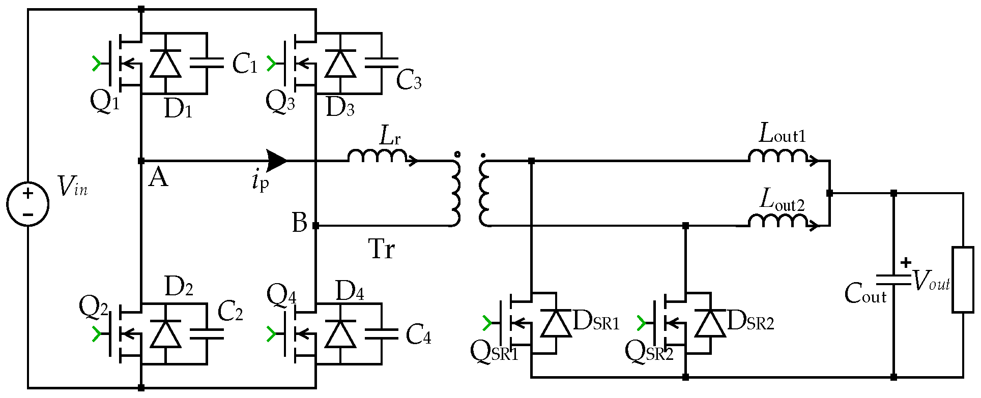
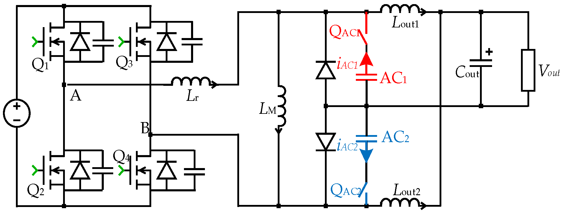
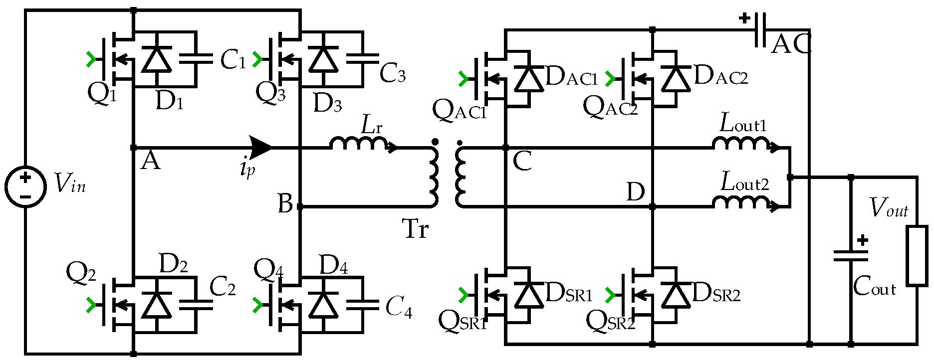
3. Improved Active Clamp Phase-Shifted Full-Bridge Converter
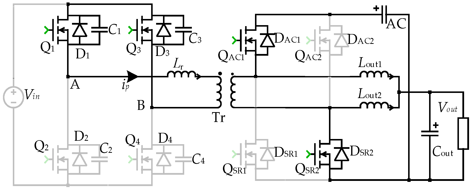
3.1. Topological Structure
- The primary side’s switches can achieve a ZVS, reducing switching losses.
- There is no circulation on the primary side of the circulation stage, which reduces the on-state loss on the primary side.
- The two synchronous rectifiers conduct at the same time to jointly refill the current for the output inductor and reduce the secondary-side pass-state losses.
- There is no loss in duty cycle because there is no current commutation time.
- The clamped synchronous rectifier on the secondary side effectively prevents secondary-side overvoltage.
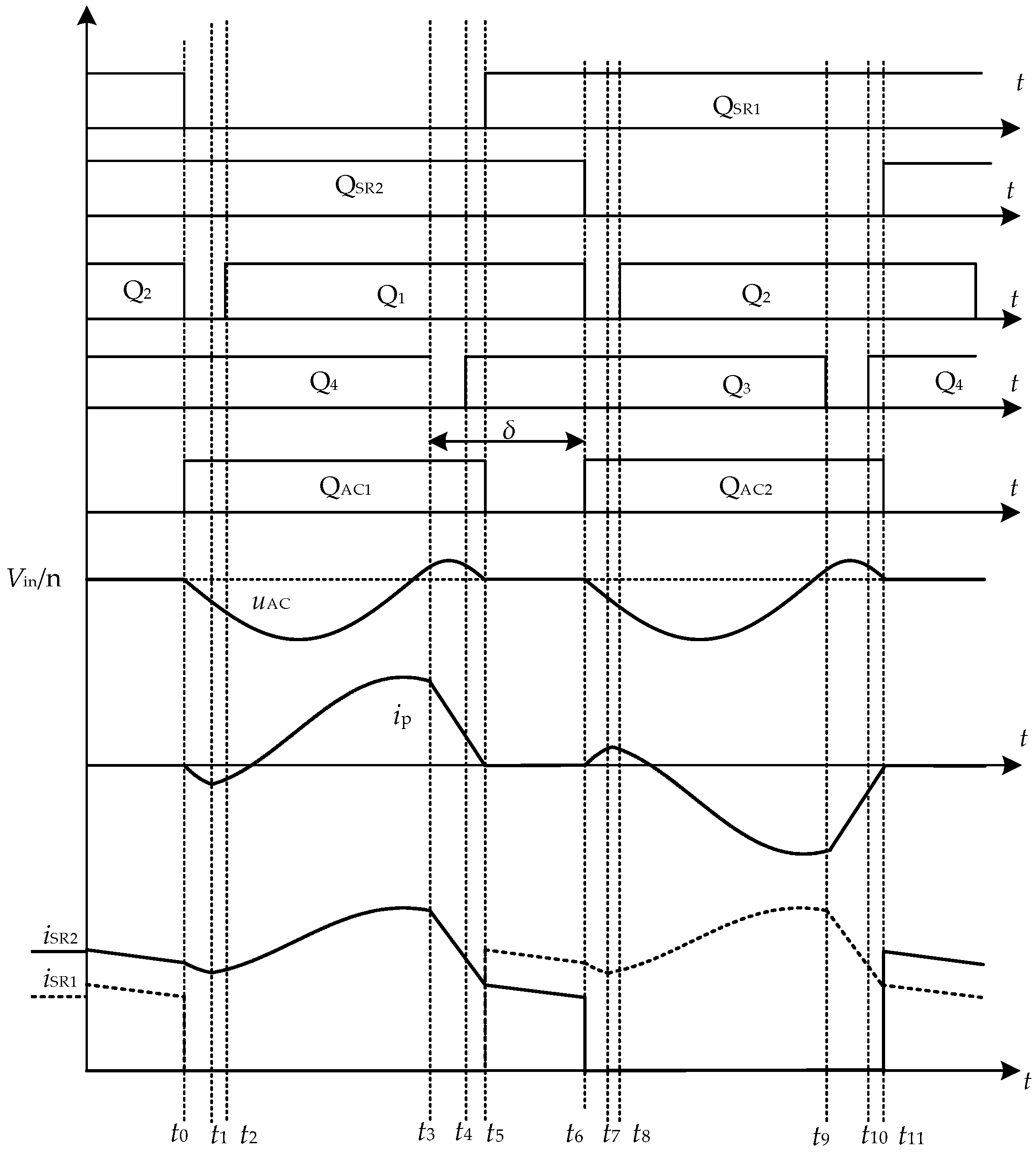
3.2. Modal Analysis
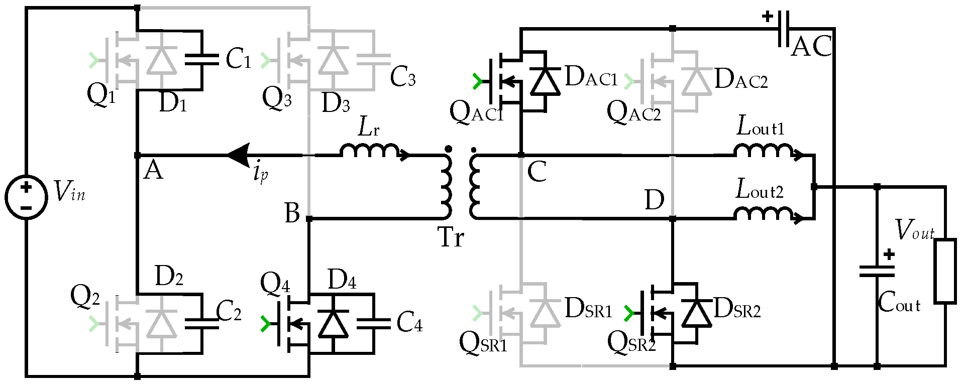
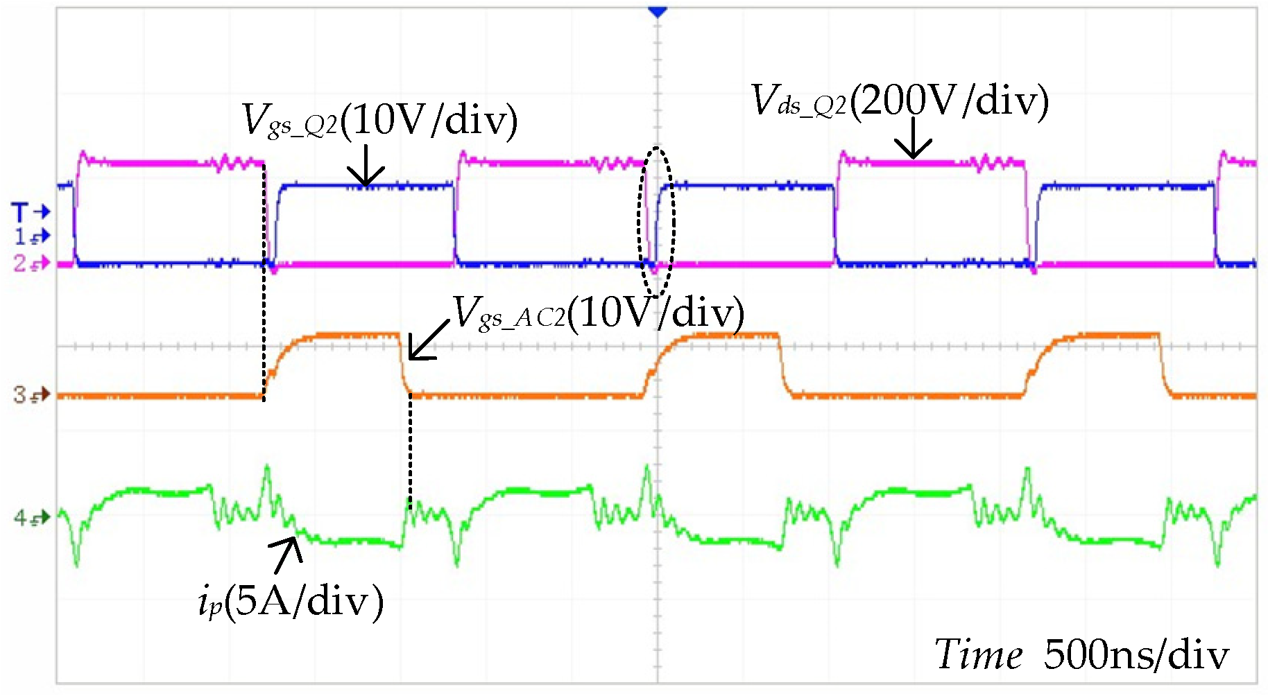
- Prior to t0, the circuit is in the loop current stage; although the switching tubes Q2 and Q4 are in the on state, there is no current flowing through it, and the primary-side current remains zero. The transformer’s primary and secondary sides are electrically isolated, and energy is not transferred from the primary side to the secondary side. The two synchronous rectifiers QSR1 and QSR2 refill the current at the same time, and the currents ILout1 and ILout2 in the output inductor of the secondary side pass through the two synchronous rectifiers QSR1 and QSR2, respectively.
- Mode 1 (t0–t1): This stage is the stage of delayed bridge arm shutdown; at time t0, Q2 is off and QAC1 is on, which connects the secondary clamp capacitor to the secondary side of the transformer. This process is very short; therefore, the clamp capacitor can be considered a constant voltage source. The equivalent circuit is shown in Figure 6. Equivalent parallel capacitors C1, C2 and the resonant inductor Lr resonate; the primary current starts at zero and increases in the negative direction in the form of a sine wave, discharging C1 and charging C2. The expressions of the primary current, the voltage at both ends of the resonant inductor, and the voltage at both ends of the parasitic capacitor C1 and C2 are as follows:
- 3.
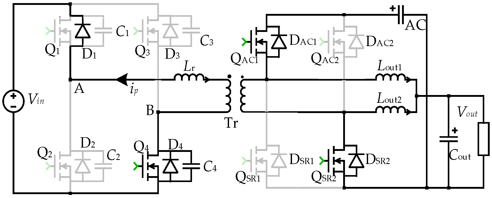
- Mode 2 (t1–t2): This stage is the lagging bridge arm ZVS turn-on phase. Figure 7 shows the equivalent circuit. At moment t1, the parasitic capacitor completes its charge–discharge process, and the body diode D1 naturally refills the current, clamping the voltage across Q1 at zero. After that, Q1 is turned on to implement the ZVS. In order to ensure that the ZVS for the lagging bridge arm switching tube can be reliably achieved, the dead time of the lagging bridge arm should be greater than the charge and discharge time; that is, the charge and discharge time of C1 and C2 is shorter than the dead time of the driver signals for Q1 and Q2. The expression is as follows:
- 4.
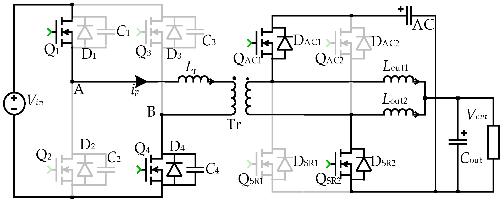
- Mode 3 (t2–t3): This stage is the power transfer phase. Figure 8 displays the equivalent circuit diagram. At t2, Q1 is turned on, and since the voltage at both ends of Q1 is zero at this time, Q1 achieves the ZVS. At this stage, both ends of the resonant inductor and clamp capacitor are directly affected by the input voltage, causing the clamp capacitor to resonate with the resonant inductor. Most of the input voltage Vin is added to the clamp capacitor through the transformer, while only a small portion of the input voltage acts on the resonant inductor. The primary side’s current is transferred from the body diode D1 to the switching tube Q1 and rises gradually in the form of a nearly sinusoidal waveform. As the primary current increases, when the current value reaches the output inductor current ILout1 value that is converted to the primary side, the clamp capacitor is converted from a discharging state to a charging state, and the volts–seconds balancing expression on the resonance inductor is as follows:
- 5.
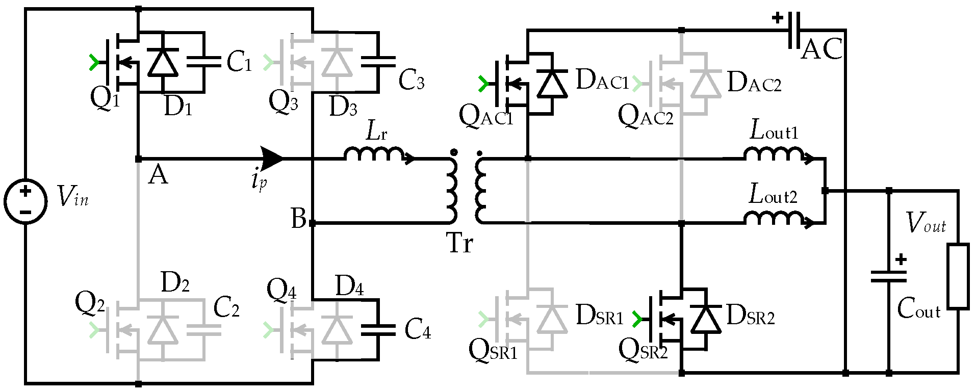
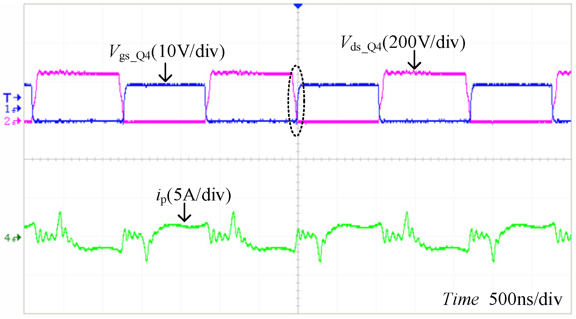
- Mode 4 (t3–t4): This stage is the stage of turning on the ZVS of the leading bridge arm and zeroing the current. Figure 9 shows the equivalent circuit. At moment t3, Q4 turns off, and the original primary current flowing through Q4 is transferred to parasitic capacitors C3 and C4, discharging C3 and charging C4 simultaneously. Due to the short charging and discharging time and the fact that the resonant inductor is connected to the secondary output inductor Lout1 and the clamp capacitors AC through the transformer, it can be thought of as a constant current source. After the charge–discharge process is completed, D3 naturally conducts, thus clamping the voltage across Q3 at zero. The time required for the whole charge–discharge process is calculated as follows:
- 6.
- Mode 5 (t4–t5): The equivalent circuit diagram is shown in Figure 10. Switch tube Q3 is turned on at moment of t4, and the leading bridge arm’s ZVS can be achieved because the voltage at both ends of Q3 is zero. At this point, the current on the primary side is transferred from the body diode D3 to Q3, and the working state of the other devices is unchanged. The clamp capacitor is connected to the primary resonant inductor through the transformer, and the voltage of the clamp capacitor is applied across the resonant inductor so that the primary current is rapidly reduced to zero. The time required for the current return to zero depends on how long the clamp tube QAC1 remains on after the switching tube Q4 is turned off. The expression is as follows:
- 7.
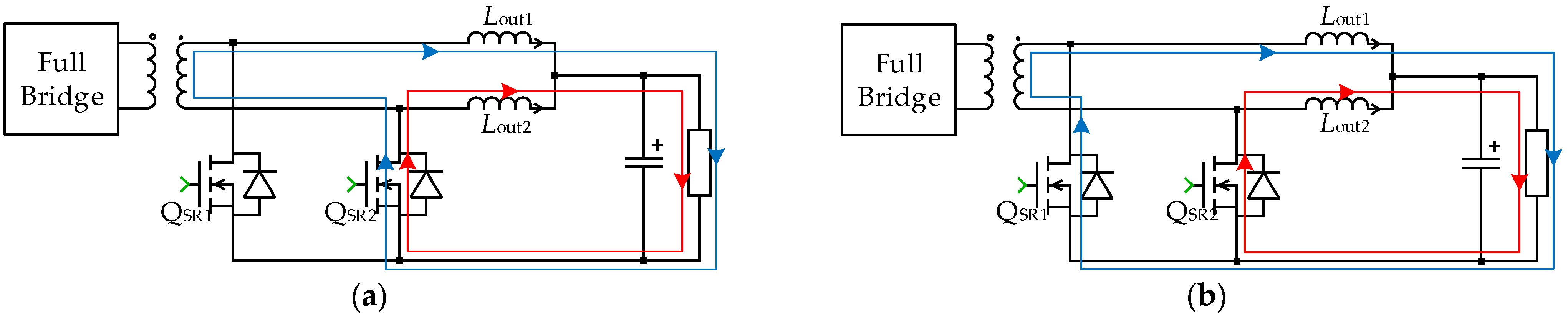
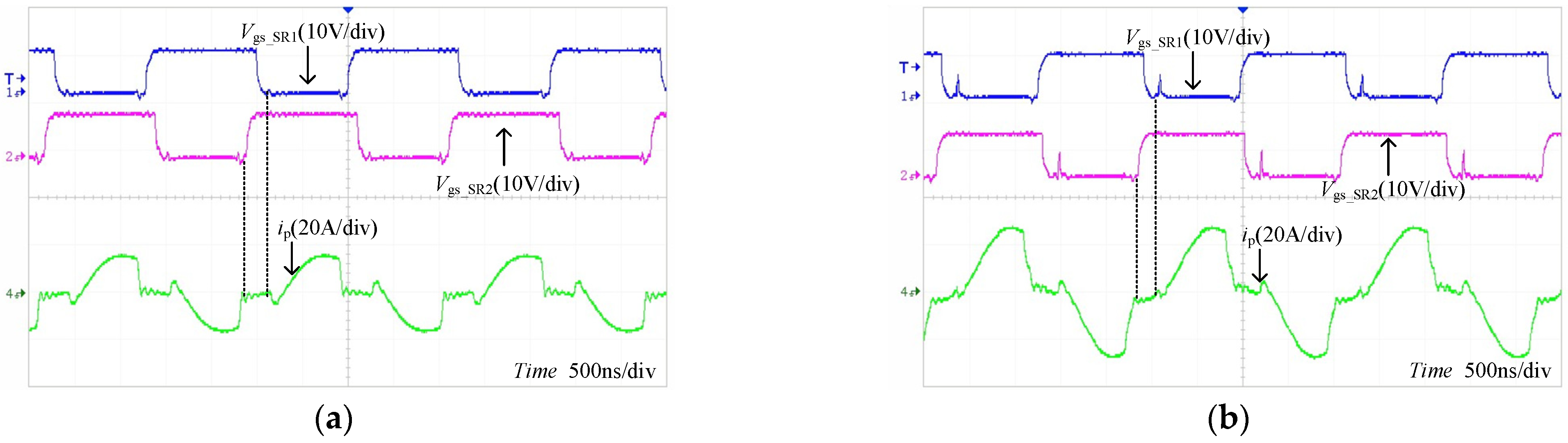
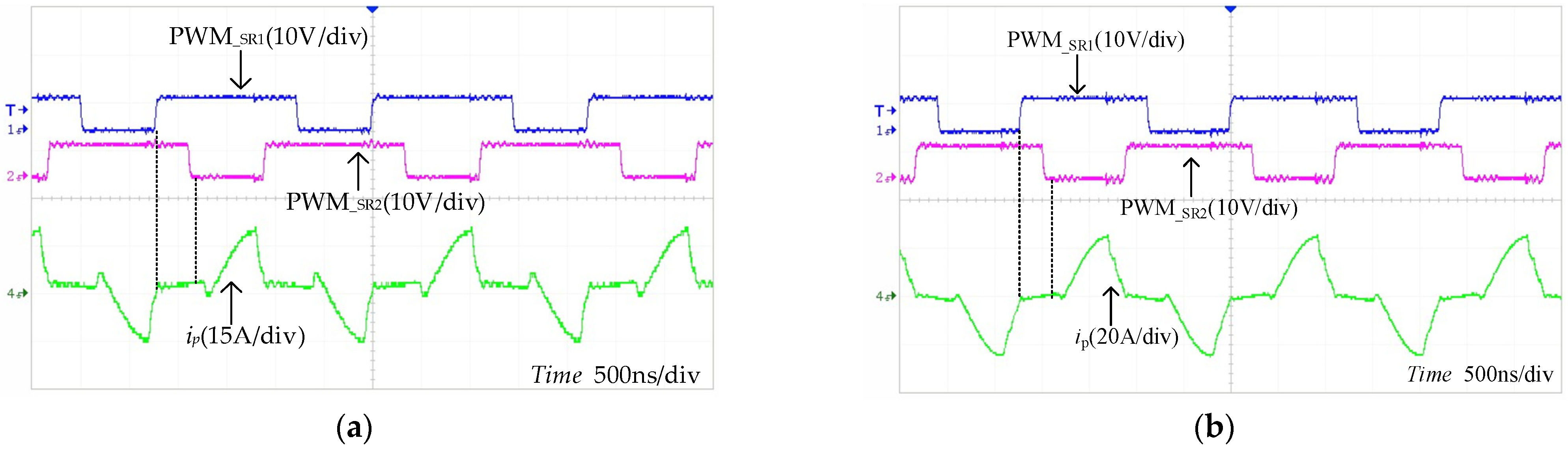
- Mode 6 (t5–t6): This stage is the circulating current stage. Figure 11 shows the equivalent circuit. At moment t5, the primary current drops to zero, and QAC1 needs to be turned off in time to prevent the current from growing in the reverse direction. Although the primary side switch tubes Q1 and Q3 remain on at this stage, the primary current is reduced to zero, and no current flows through Q1 and Q3, resulting in no circulation on the primary side and significantly reducing the primary loss during the on state. The two synchronous rectifier tubes QSR1 and QSR2 are switched on at the same time, the transformer is short-circuited, the voltage at both ends of the transformer drops to zero, and the original secondary side is decoupled. In addition, the secondary winding of the transformer carries no current, and the synchronous rectifier tubes QSR1 and QSR2 provide a continuous current path for the output inductance Lout1 and Lout2, respectively, to share the output current. In contrast to the traditional phase-shifted full-bridge mode of continuous flow only through a single rectifier tube, the RMS (Root Mean Square) current and on-state loss in the synchronous rectifier switching tubes are significantly reduced. The on-state loss on both the primary and secondary sides has been effectively reduced.
4. Principle of Operation and Characteristics
4.1. Lagging Bridge Arm ZVS
4.2. Low On-State Loss
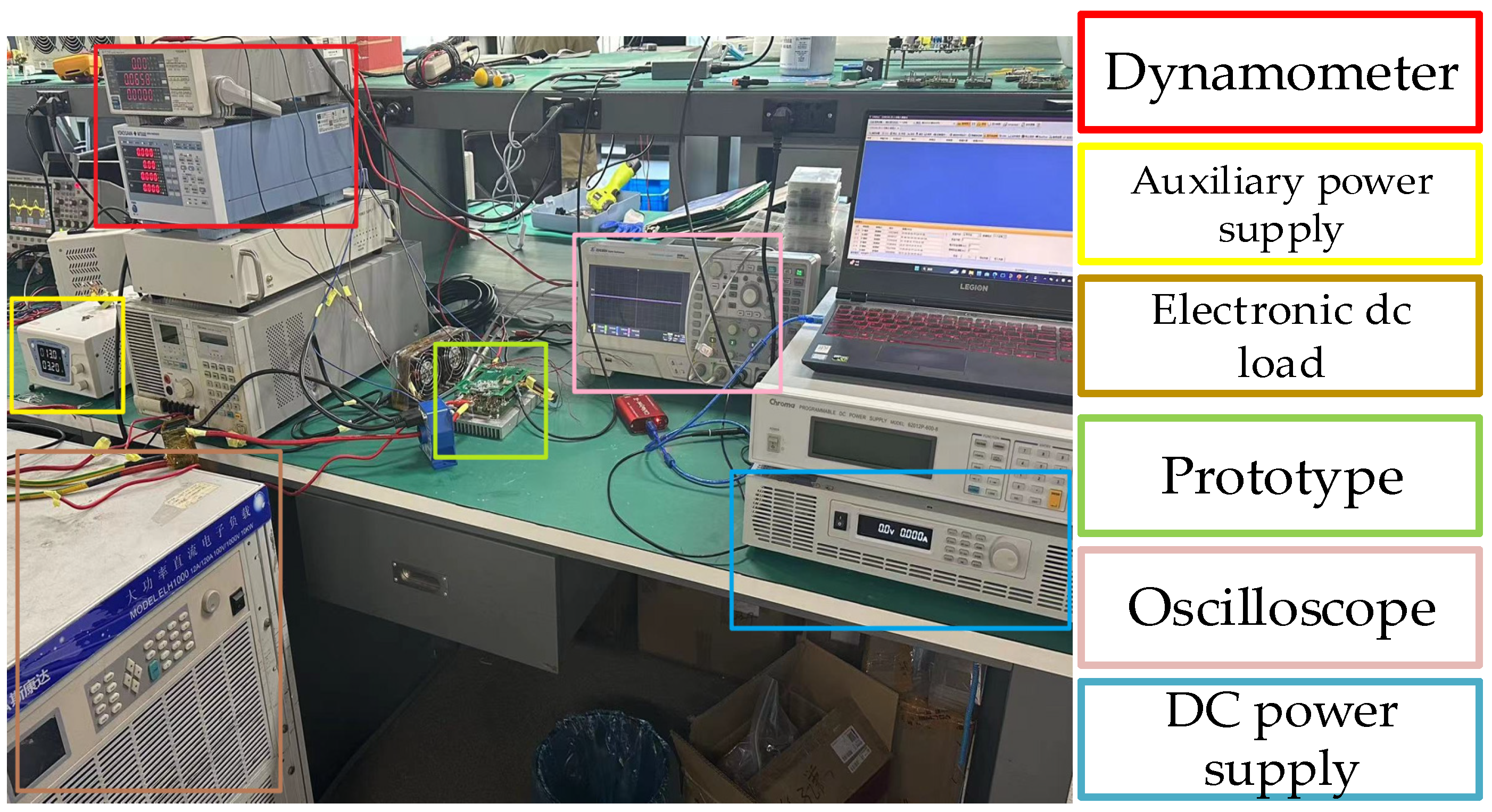
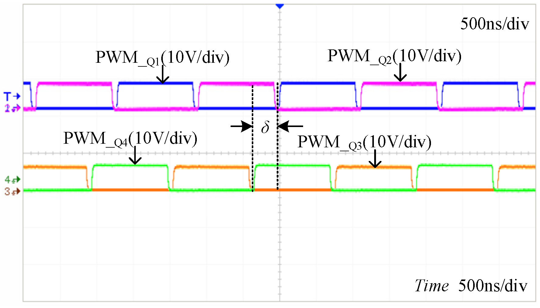
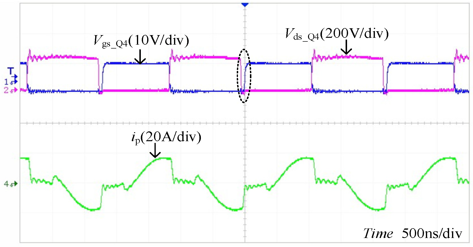
5. Test Result
5.1. ZVS Waveform Analysis
5.2. On-State Loss Analysis
5.3. Efficiency Curve
6. Conclusions
Author Contributions
Funding
Data Availability Statement
Acknowledgments
Conflicts of Interest
References
- Zhou, J.H.; Wang, J.B. Research Review on Multi-Port Energy Routers Adapted to Renewable Energy Access. Electronics 2023, 13, 1493. [Google Scholar] [CrossRef]
- Meng, X.L.; Duan, Q.; Sha, G.L.; Zhao, C.H.; Wang, H.Q.; Wang, X.L.; Lan, Z. An Efficiency Improvement Strategy for Triple-Active-Bridge-Based DC Energy Routers in DC Microgrids. Electronics 2024, 13, 1172. [Google Scholar] [CrossRef]
- Zhang, Z.X.; Jian, P. Review of Research on Phase-shifted Full-bridge ZVS DC-DC Converter. J. Power Supply 2022, 20, 11–27. [Google Scholar]
- Hua, G.; Lee, F.C.; Jovanovic, M.M. An improved full-bridge zero-voltage-switched PWM converter using a saturable inductor. IEEE Trans. Power Electron. 1993, 8, 530–534. [Google Scholar] [CrossRef]
- Deng, Y.J.; Zhao, N.; Wu, J.J.; Zhou, H.J. Research on Optimization Method of Soft-Switching Range of DAB Converter Based on Saturable Inductor. In Proceedings of the 2020 Asia Energy and Electrical Engineering Symposium (AEEES), Chengdu, China, 29–31 May 2020. [Google Scholar]
- Kwon, B.H.; Kim, J.H.; Jeong, G.Y. Full-bridge soft switching PWM converter with saturable inductors at the secondary side. IEE Proc.-Electr. Power Appl. 1999, 146, 117–122. [Google Scholar] [CrossRef]
- Safaee, A.; Bakhshai, A.; Jain, P. An efficient adaptive energy storage using saturable inductors for ZVS phase-shift-modulated full-bridge converters. In Proceedings of the 2010 International Conference on Power, Control and Embedded Systems, Allahabad, India, 29 November–1 December 2010. [Google Scholar]
- Redl, R.; Sokal, N.O.; Balogu, L. A novel soft-switching full-bridge DC/DC converter: Analysis, design considerations, and experimental results at 1.5 kW, 100 kHz. IEEE Trans. Power Electron. 1991, 6, 408–418. [Google Scholar] [CrossRef]
- Heintze, M.; Butzmann, S. A GaN 500 kHz High Current Active Clamp Phase-Shifted Full-Bridge Converter With Zero-Voltage Switching Over the Entire Line and Load Range. In Proceedings of the 2018 20th European Conference on Power Electronics and Applications (EPE’18 ECCE Europe), Riga, Latvia, 17–21 September 2018. [Google Scholar]
- Mahapatra, M.; Pal, A.; Basu, K. Effects of Parasitics on An Active Clamp Assisted Phase Shifted Full Bridge Converter Operation. In Proceedings of the 2021 IEEE Energy Conversion Congress and Exposition (ECCE), Vancouver, BC, Canada, 10–14 October 2021. [Google Scholar]
- Yan, X.Y.; Zhu, Y.R.; Wang, Z.Y.; Yang, T.; Bozhko, S.; Wheeler, P. Dual Phase Shift Modulation Investigation of Half-Bridge-Active-Clamp Converter for Future Electrified Aircraft Applications. In Proceedings of the 2023 IEEE Workshop on Power Electronics for Aerospace Applications (PEASA), Nottingham, UK, 18–19 July 2023. [Google Scholar]
- Li, N.; Zhang, C.J.; Liu, Y.H.; Zhuo, C.R.; Liu, M.; Yang, J.L.; Zhang, Y. Single-Degree-of-Freedom Hybrid Modulation Strategy and Light-Load Efficiency Optimization for Dual-Active-Bridge Converter. IEEE J. Emerg. Sel. Top. Power Electron. 2024, 12, 3936–3947. [Google Scholar] [CrossRef]
- Gu, B.; Lai, J.S.; Kees, N.; Zheng, C. Hybrid-switching full-bridge DC–DC converter with minimal voltage stress of bridge rectifier, reduced circulating losses, and filter requirement for electric vehicle battery chargers. IEEE Trans. Power Electron. 2012, 28, 1132–1144. [Google Scholar] [CrossRef]
- Ruan, X.B.; Yan, Y.G. A novel zero-voltage and zero-current-switching PWM full-bridge converter using two diodes in series with the lagging leg. IEEE Trans. Ind. Electron. 2001, 48, 777–785. [Google Scholar] [CrossRef]
- Chen, J.X.; Zhang, J.W.; Zhou, J.Q.; Shi, G.; Jia, Y.J.; Wang, H.; Cai, X. Enhanced Modular Multilevel Converter with Multiple MVac Ports Based on Active Fundamental-Frequency Circulating Current Injection to Realize Full-Range Operation. IEEE Trans. Power Electron. 2024, 40, 5423–5439. [Google Scholar] [CrossRef]
- Lin, H.J.; Cai, C.S.; Chen, J.Y.; Gao, Y.; Vazquez, S.G.; Li, Y.W. Modulation and Control Independent Dead-Zone Compensation for H-Bridge Converters: A Simplified Digital Logic Scheme. IEEE Trans. Ind. Electron. 2024, 71, 15239–15244. [Google Scholar] [CrossRef]
- Fan, S.G.; Gong, B.; You, J.; Sun, L.; Duan, J.D. Active Clamped ZVS Soft Switching Technology With Low Voltage and Current Stress. Proc. CSEE 2021, 41, 4616–4627. [Google Scholar]


Disclaimer/Publisher’s Note: The statements, opinions and data contained in all publications are solely those of the individual author(s) and contributor(s) and not of MDPI and/or the editor(s). MDPI and/or the editor(s) disclaim responsibility for any injury to people or property resulting from any ideas, methods, instructions or products referred to in the content. |
© 2025 by the authors. Licensee MDPI, Basel, Switzerland. This article is an open access article distributed under the terms and conditions of the Creative Commons Attribution (CC BY) license (https://creativecommons.org/licenses/by/4.0/).
Share and Cite
Guo, X.; Meng, R.; Bai, X.; Li, H.; Zhang, J.; He, X. Study of Improved Active Clamp Phase-Shifted Full-Bridge Converter. Electronics 2025, 14, 834. https://doi.org/10.3390/electronics14050834
Guo X, Meng R, Bai X, Li H, Zhang J, He X. Study of Improved Active Clamp Phase-Shifted Full-Bridge Converter. Electronics. 2025; 14(5):834. https://doi.org/10.3390/electronics14050834
Chicago/Turabian StyleGuo, Xinyao, Runquan Meng, Xiang Bai, Huajian Li, Jiahui Zhang, and Xin He. 2025. "Study of Improved Active Clamp Phase-Shifted Full-Bridge Converter" Electronics 14, no. 5: 834. https://doi.org/10.3390/electronics14050834
APA StyleGuo, X., Meng, R., Bai, X., Li, H., Zhang, J., & He, X. (2025). Study of Improved Active Clamp Phase-Shifted Full-Bridge Converter. Electronics, 14(5), 834. https://doi.org/10.3390/electronics14050834