Article

Quad-Beam 4 × 2 Array Antenna for Millimeter-Wave 5G Applications

by
Parveez Shariff Bhadravathi Ghouse
1,
Tanweer Ali
1,*,
Pallavi R. Mane
1,
Sameena Pathan
2,
Sudheesh Puthenveettil Gopi
1,
Bal S. Virdee
3,
Jaume Anguera
4,5 and
Prashant M. Prabhu
1
1
Department of Electronics and Communication Engineering, Manipal Institute of Technology, Manipal Academy of Higher Education, Manipal 576104, India
2
Department of Information and Communication Technology, Manipal Institute of Technology, Manipal Academy of Higher Education, Manipal 576104, India
3
Center for Communication Technology, London Metropolitan University, London N7 8dB, UK
4
Ignion, 08174 Barcelona, Spain
5
Research Group on Smart Society, La Salle Engineering, Universitat Romon Llull, 08022 Barcelona, Spain
*
Author to whom correspondence should be addressed.
Electronics 2025, 14(5), 1056; https://doi.org/10.3390/electronics14051056
Submission received: 3 February 2025 / Revised: 26 February 2025 / Accepted: 28 February 2025 / Published: 6 March 2025

Abstract

:
This article presents the design of a novel, compact, 4 × 2 planar-array antenna that provides quad-beam radiation in the broadside direction, and it enhances coverage and serviceability for millimeter-wave applications. The antenna utilizes a corporate (parallel) feed network to deliver equal power and phase to all elements. Non-uniform element spacing in the two orthogonal planes, exceeding 0.5 λ 1 ( λ 1 being the wavelength at 30 GHz), results in a quad-beam radiation pattern. Two beams are formed in the xz-plane and two in the yz-plane, oriented at angles of θ = ± 54 ° . However, this spacing leads to null radiation at the center and splits the radiation energy, reducing the overall gain. The measured half-power beamwidth (HPBW) is 30° in the xz-plane and 35° in the yz-plane, with X-polarization levels of −20.5 dB and −26 dB, respectively. The antenna achieves a bandwidth of 28.5–31.1 GHz and a peak gain of 10.6 dBi. Furthermore, increasing the aperture size enhances the gain and narrows the beamwidth by replicating the structure and tuning the feed network. These features make the proposed antenna suitable for 5G wireless communication systems.

1. Introduction

The millimeter-wave (mmWave) spectrum has garnered significant attention due to its ability to offer wide bandwidth and low latency in signal propagation, making it ideal for high-speed data communications and advanced sensing applications. mmWave technology spans a broad range of applications, including both communication and non-communication fields. For instance, mmWave has been employed in radar-based techniques to monitor electrocardiograms (ECGs) [1]. Its application extends across various domains, such as cellular communication, health monitoring [1], vehicular communication [2], and robotic control systems [3].
A key enabler of these applications is the antenna, which plays a central role in ensuring the efficient transmission and reception of mmWave signals. Numerous design methodologies have been explored to realize effective antennas for mmWave frequencies [4,5,6,7,8,9]. Among these, planar structures [10] have attracted particular interest due to their compact size, ease of integration, and low-profile configuration. However, planar antennas inherently suffer from lower gain due to their limited aperture size [11,12]. To address this limitation, array configurations are often employed to enhance gain by increasing the effective aperture area [4].
Multi-beam antennas are especially advantageous in modern wireless communication systems as they facilitate improved beam scanning, enabling wider coverage and allowing more devices or users to connect with a minimal interface. In [7], a complex, leaky wave antenna (LWA) was designed to achieve a quad-beam. Another design in [13] employed a combination of LWA with a substrate-integrated waveguide (SIW) to obtain a quad-beam. However, both designs were intricate and cumbersome due to their large and complex structures. Similarly, in [14], an inclined planar antenna etched with a U-shaped slot and SIW cavity was introduced to achieve circular polarization. The 45° inclination of the patch and the slot improved polarization, but the SIW feed mechanism contributed to further structural complexity. In [15], multiple patch rings were stacked across different layers, using two orthogonal feeds to achieve dual polarization. To prevent leakage and ensure efficient coupling, an SIW structure was embedded in the feed layer, further completing the design.
Simplifying antenna architecture has been a subject of ongoing research. For example, the authors of [16] demonstrates a planar Fracklin array structure with a series feed, reducing complexity by integrating a patch and feed network on the same plane. In this case, the antenna was able to achieve a dual beam at ±45°. In [17], a straightforward design transformed a non-radiating microstrip line into a radiating element by introducing inverted cone patches at half-wavelength intervals, canceling the antiphase magnetic fields commonly associated with conventional microstrip lines. One of the methods for generating a simultaneous beam is the use of RF circuitry through which the sub-set of an array is activated, thus achieving a dual beam in the azimuthal and the other two in the elevation plane [18]. Similarly, in [19], researchers also demonstrated a multi-beam pattern in the azimuthal plane using a PIN diode and RF circuitry. However, both these structures, due to their RF circuitry, were complex. In another approach, in [20], a curved linear array structure with a non-uniform spacing technique was adopted to form a multi-beam at varied elevation angles. This method is appropriate for smaller array structures achieving decent gain; however, it poses limitations when increasing the antenna aperture for achieving a high-gain performance.
Thus, this article focuses on the design of a novel planar array antenna that addresses the above design challenges by strategically placing an array structure to achieve a quad-beam. With quad-beam behavior, the device can simultaneously communicate with two user devices in the azimuthal plane and another two in the elevation plane. The single-element antenna presented in this article is a figure-eight-shaped elliptical ring. The literature has illustrated several elliptical-shaped antennas with defected ground structures for impedance matching over wide bandwidths. For example, in [21,22], the ground planes were defected for impedance matching over a wide bandwidth at the cost of reduced radiation directivity. However, the single-element antenna structure documented in this article is a novel figure-eight-shaped elliptical ring. Better impedance matching is achieved by altering the geometry of the patch rather than the ground plane so that the antenna can simultaneously achieve better resonance and directivity.
Further, the directivity and gain are enhanced by configuring the single-element antenna to a 4 × 2 array with a corporate (parallel) feed network, ensuring equal power and phase distribution across all elements. The compact structure has dimensions of 2.02 λ 1 × 1.82 λ 1 (where λ 1 is the wavelength at 30 GHz). The design leverages non-uniform element spacing to form a quad-beam pattern, with a detailed analysis provided on the radiation characteristics and beam formation mechanism. The proposed antenna achieves a maximum gain of 10.6 dBi, potentially improving further gain by replicating and modifying the feed network. The design is well-suited for 5G wireless communication applications, where high-gain, multi-beam capabilities are critical for a robust performance.

2. Single-Element Antenna

2.1. Design Procedure

The single-element antenna is a highly compact structure etched on a Rogers 5880 substrate, which has a relative permittivity of 2.2 and thickness of 0.254 mm. The design operates at a wavelength of λ 1 (where λ 1 is a wavelength at 30 GHz). The base design is a dual-ellipse configuration derived from a conventional circular patch [23].
A typical circular patch antenna with a radius of 1.82 mm generates resonance at λ 1 , resulting in a total area of 10.40 mm2. This circular area is divided into two elliptical sections to form a dual-ellipse structure in the proposed design. Each elliptical section has a major axis (Eh1), which determines the resonance of the antenna, the dimension of which is derived from the cavity model Equation (1) for the TM10 operation mode. The dimension of the minor axis (Ev1) significantly affects the impedance matching and tuning the resonance, which is judicially chosen.
f 1 = c 2 π ε e f f · m E h 1 2 + n E v 1 2 ,
where c is 3 × 10 8 (m/s) and ε e f f is the relative permittivity, which is approximately 1.6 in this case. The m and n are fundamental modes along the x-axis and y-axis, respectively. In this case, m = 1 and n = 0, and then the resulting Eh1 is equal to 3.95 mm for 30 GHz. Further, this is tuned to 3.74 mm to obtain a better result with a minor axis (Ev1) of 1.7 mm, providing an individual area of approximately 5 mm2. Together, the two elliptical sections closely match the area of the original circular patch. As illustrated in Figure 1a, the dual-ellipse design is implemented to increase the effective antenna aperture, thereby enhancing gain. The antenna achieves improved surface current distribution and overall performance by redistributing the area in two elliptical structures. A quarter-wave transformer with a guided wavelength of λ g long at 30 GHz and having an impedance of 75 Ω is used to feed the antenna, aiming to match the antenna impedance with the port. However, a significant impedance mismatch is observed, as depicted by the surface current distribution shown in Figure 1b.
The antenna’s initial impedance is measured to be 2.84 j 2.38 Ω, indicating a short current path and low reactance. This low impedance suggests that the patch antenna presents minimal resistance to the surface currents.
To address this issue, the impedance is adjusted by increasing the electrical length of the oscillating current. This is achieved by introducing elliptical slots within both elliptical structures of the antenna, as shown in Figure 2. Now, due to the slot, the electrical length is close to 3.74 mm, which results in improved resonance at 30 GHz, as evidenced by the cavity model in Equation (1). The slots extended the current path, resulting in a substantial increase in reactance. The modified antenna impedance is measured as 59.32 j 21.74 Ω, bringing it closer to the target of 50 Ω. This improvement is further illustrated through the surface current distribution shown in Figure 3a.
Despite these modifications, the bandwidth remains relatively narrow, ranging from 30.12 to 30.56 GHz. Efforts to enhance the impedance match and current distribution have contributed to improved antenna performance within this frequency range.
The single-element antenna (Ant1) achieved a peak gain of 7.8 dBi, as shown in Figure 4a. With a fully grounded structure at the bottom, the radiation is directed in the broadside direction. The half-power beamwidth (HPBW) is measured to be 71° in the xz-plane and 56° in the yz-plane. Ant1 demonstrates excellent X-polarization performance in the xz-plane, while the X-polarization in the yz-plane is acceptable, as illustrated in Figure 4b.
The electric field (E-field) energy in the E-plane exhibits linear polarization, aligning vertically along the x-axis at the resonance frequency, thereby generating vertical polarization. However, the slotted elliptical structure causes opposing magnetic field components, which results in higher X-polarization in the H-plane. This behavior is further explained through the Poynting vector representation shown in Figure 5, which highlights the field interaction and polarization effects within the antenna structure. The Poynting vector determines the direction of propagation through the product of electric and magnetic components. The radiated electromagnetic wave in the far field region is independent of distance, and it should have the real part of the Poynting vector and be free from the imaginary part to achieve maximum power transfer [24,25]. The higher the magnitude of the Poynting vector, the higher the radiated power. In Figure 5, the red arrows indicate the higher magnitude vectors, and these high-magnitude vectors are aligned vertically and partly horizontally; as a result, a high X-polarization has occurred, as depicted in Figure 4b.

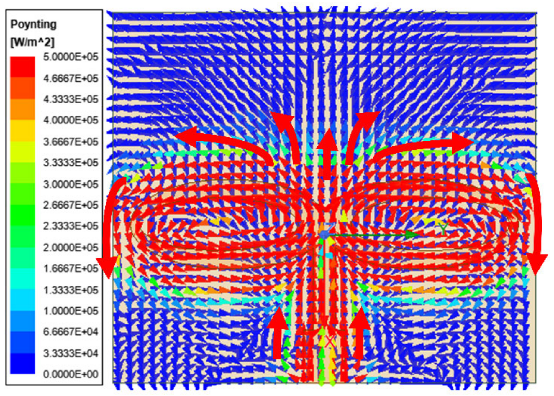
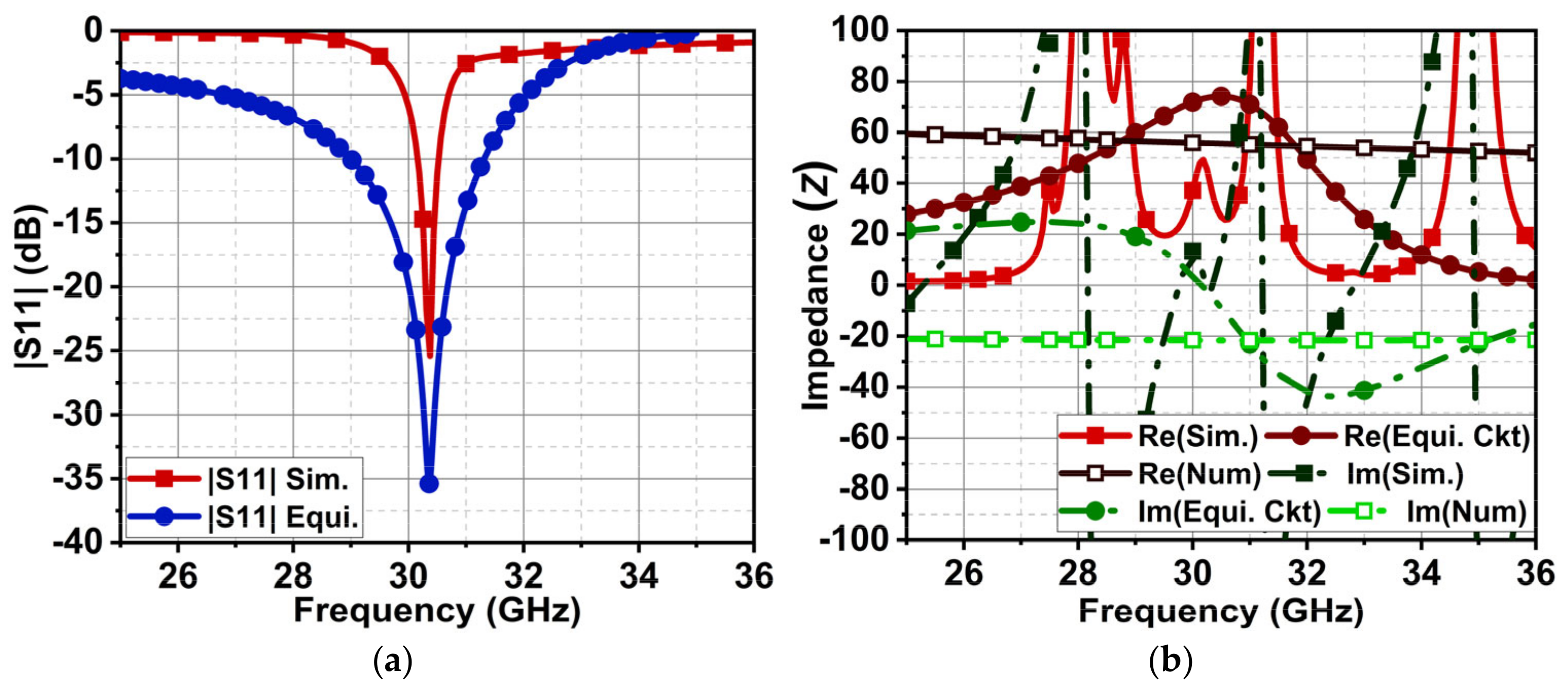
2.2. Antenna Modeling Using Transmission Line

In the previous section, the antenna structure is designed and tuned using the finite-element method (FEM), which provides the overall response of the antenna structure. However, it does not provide insight into the part-by-part structure behavior, and this can be comprehended by transforming the antenna geometry to a transmission line model. The transmission line model offers detailed insight into the changes in the impedances in figure-eights at distinct points, as well as the effects of feed line and ground. Thus, this section discusses the above antenna transmission line model in detail.
At mmWave, the dimension of the proposed antenna is comparable with the wavelength; as a result, the voltage and current on the structure at different points vary, and consequently, the phase changes. Thus, the modeling of the antenna as a parallel RLC circuit does not fully comply. As a result, we split the entire structure into small lengths of transmission line, as shown in Figure 6, and we apply the transmission line theory to find the total impedance ( Z T ) at the input. The conducting area of the patch is transformed to multiple series inductances at different points due to varying conductive widths. Likewise, the slot in the patch is transformed into the shunt capacitance connected between the series inductive impedances. The same principle is applied to the feed and ground layer. This impedance circuit is realized in the circuit simulator and tuned to achieve the desired response. Further, the total input impedance is computed using the transmission line equations.
Z I T is the intermediate impedance at the input of the quarter-wave transformer, with a quarter-wave transform impedance of 75 Ω. The load impedance ( Z L ) is the impedance of two elliptical rings, which are further split as impedances Z 1 , Z 2 , and Z c 1 . The elliptical ring has varied widths; consequently, its impedance also varies. Thus, it is modeled with two impedances, Z 1 and Z 2 . The capacitance effect in the ring is represented by the shunt capacitive impedance Z c 1 . Z c 2 and Z c g are the coupling capacitors between the patch and the ground plane. Therefore, the load impedance Z L and ground impedance Z g are obtained using Equations (2)–(10), as follows:
Z L = Z 1 c 2   Z 1 c 2 Z 1 c 2 + Z 1 c 2 ,
where
Z c 12 = Z C 11 = Z 1 Z c 1 2 Z 1 + Z c 1 ,
Z 11 = Z 1 2 2 Z 1 + Z c 1 ,
Z c 112 = Z c 113 = Z c 11 + Z 2   ,
Z p = Z c 112   Z c 113 Z c 112 + Z c 113 ,
Z 1 c 2 = Z 11 + Z p + Z c 2 ,
Z L = Z 1 c 2   Z 1 c 2 Z 1 c 2 + Z 1 c 2 , and
Z L g 1 = Z L g   Z L g Z L g + Z L g .
Z g = Z c g + Z L g 1        
The load and ground impedance together are obtained by Z L g d , as follows:
Z L g d = Z L   Z g Z L + Z g .
Due to the quarter-wave transform, the input impedance Z I T is obtained as follows:
Z I T = ( Z F l 1 ) 2 Z L g d .
Further applying the transmission line equation, the total input impedance is obtained as follows:
Z T = Z F l 1   Z I T + j Z F l 1   t a n ( β 1 l 1 ) Z F l 1 + j Z I T t a n ( β 1 l 1 ) ,
where β 1 and l 1 are the phase constant and length, respectively, of the impedance Z F l 1 . The Figure 6 is modeled in the circuit simulator to find its impedances. The reflection coefficient graph of the simulated and modeled antenna is compared in Figure 7a. From the circuit simulator, the obtained impedances are Z 1 = 27.1 + 77.28 j , Z 2 = 8.2 + 50.89 j , Z c 1 = 53.05 j , Z c 2 = 15.6 j , Z c g = 84.2 j , and Z l g = 111.21 j . Substituting these impedances in the above equations results in the load impedance Z L = 8.82 + 24.24 j and the ground impedance Z g = 28.59 j . The obtained intermediate impedance Z I T i s   74.58 8.16 j and the total input impedance Z T   i s   55.91 21.63 j . The impedance graph from the numerical method is compared with the results of the FEM and circuit simulator shown in Figure 7b. The numerically estimated input impedance is close to 50 Ω; however, it shows slight capacitive impedance, and this is due to the shunt capacitance effect. Nonetheless, the modeled antenna reflects the 50 Ω characteristics at 30.4 GHz.

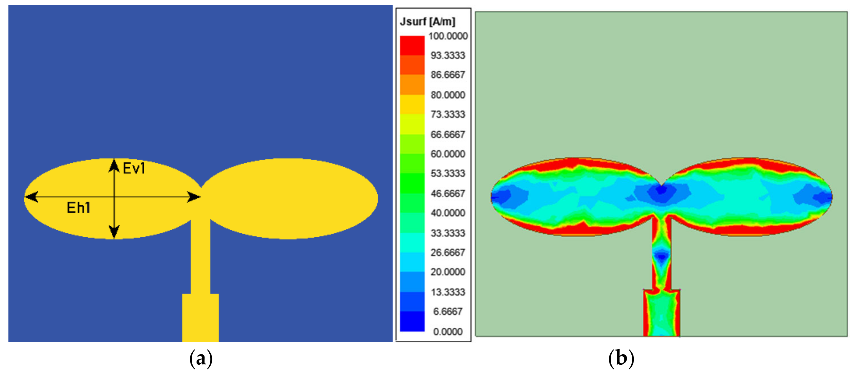
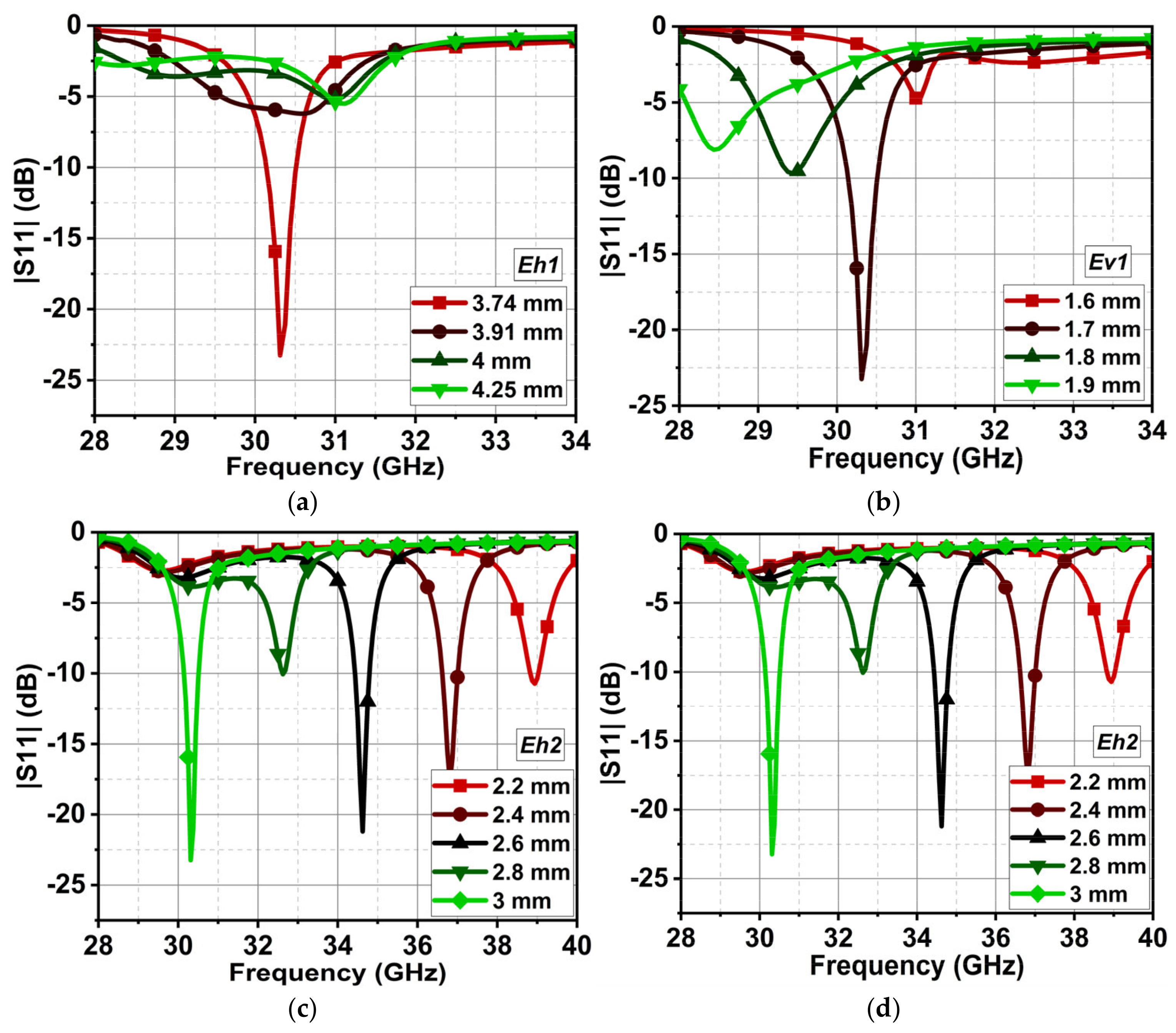
2.3. Parametric Analysis of the Single-Element Antenna

In this section, the effect of the reflection coefficient and drift in the resonance frequency of the single-element antenna (Ant1) are discussed due to the variations in the major (Eh1) and minor (Ev1) axes of the elliptical patch and the major (Eh2) and minor (Ev2) axes of the elliptical slot. Figure 8a,b illustrates that the changes in the length and width of the elliptical patch significantly impact the impedance matching. In fact, the increase in the width of the patch increases the area and the length of the electrical current, thus drifting the resonance to a lower frequency, though with poor impedance matching.
On the other hand, the elliptical slot plays a vital role in impedance matching and tuning the resonance frequency to the desired response. Figure 8c,d demonstrates that the electrical current taking the shortest path is the slot’s circumference, where the conductive area exists. As a result, for a smaller major axis (Eh2), the antenna results in resonance at a higher frequency. Further, with an increased Eh2, the resonance drifts to the lower frequency. A similar effect is observed for the change in Ev2. Thus, the resonance can be varied with the slot length and width.

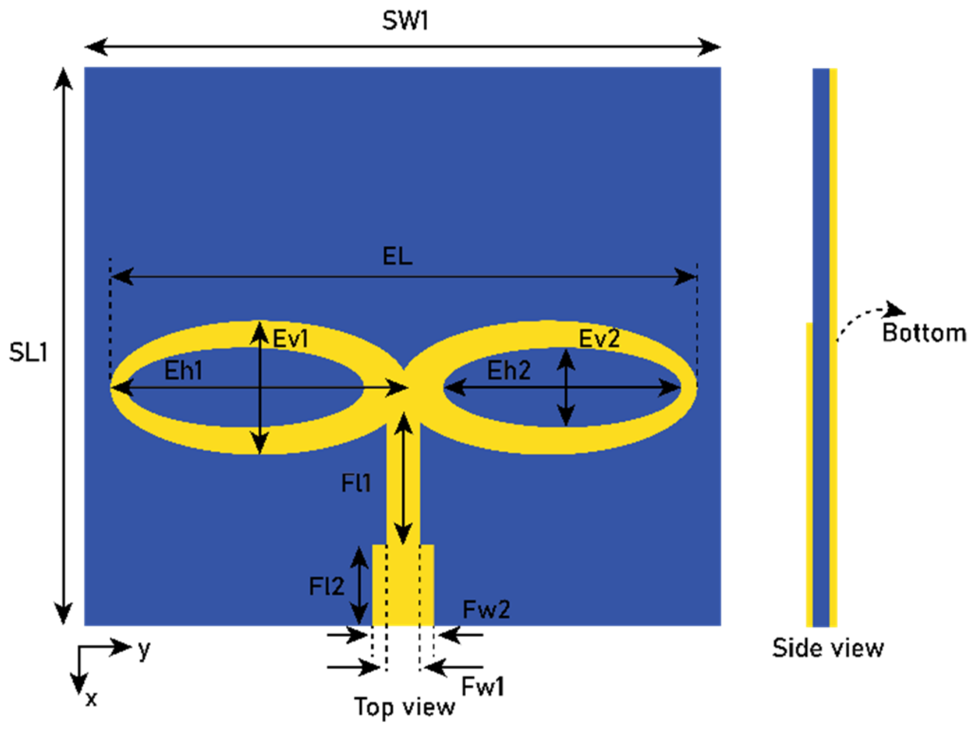
3. Array Antenna Design

In an array antenna, increasing the aperture size leads to higher gain. However, one of the major challenges is designing an efficient feed network that can distribute power evenly across all elements. To address this, Ant1 is transformed into an array structure using a parallel feed network. This approach simplifies the design while ensuring that equal power and phase are delivered to each element. Additionally, a slight improvement in bandwidth is observed with the array configuration.
In the case of Ant1, the elliptical structure spans 0.74 λ 1 along the y-axis, which necessitates an inter-element spacing of greater than λ 1 / 2 to minimize the mutual coupling effects. However, this spacing also contributes to the formation of grating lobes, which result in a distinctive quad-beam radiation pattern. The evolution of the radiation behavior has been systematically studied, progressing from a basic 2 × 1 array to the final 4 × 2 array configuration. This progression demonstrates how non-uniform spacing and array geometry play critical roles in achieving the desired multi-beam performance.

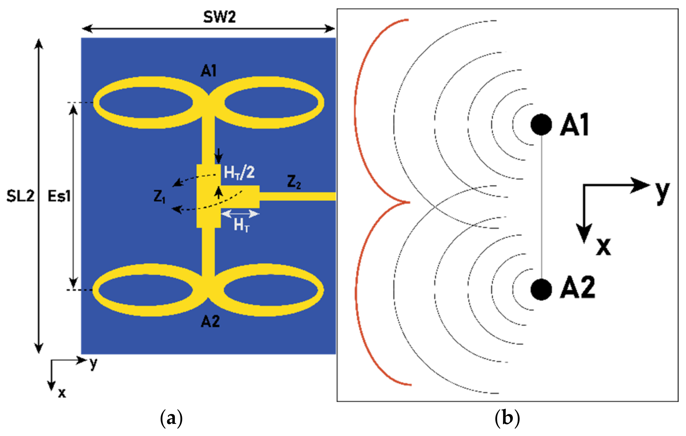
3.1. A 2 × 1 Array Antenna

A 2 × 1 array structure (Ant2), as shown in Figure 9a, is designed and analyzed for its radiation pattern. The interelement spacing (Es1) along the x-axis is 0.6 λ 1 , which is slightly greater than a half-wavelength. Equal power is split between A1 and A2 with the aid of a T-junction stub having an impedance of Z1. The splitting stub length is half of the injection stub. To feed the power to the T-splitter, a feed line length is tuned to Z2 (where Z1 = 50 Ω and Z2 = 100 Ω).
The radiation pattern is well described by the array factor (AF). For a two-element linear array, A F = I 1 e j ( 0 ) + I 2 e j ( Ψ ) . Since both antennas are provided with equal power, where k is the wavenumber, β is the phase difference between elements and I = I 1 = I 2 . Applying Eulers rule and simplifying leads to the following:
A F = I 1 + e j ( k E s 1 c o s θ + β ,
where k is the wavenumber, β is the phase difference between elements, and I = I 1 = I 2 . Applying Eulers rule and simplifying leads to the following:
A F = 2 I c o s k E s 1 cos θ + β 2       .
Since the parallel feed mechanism is used, the phase difference ( β ) between the elements will be zero. Equation (15) is fed to the Matlab tool to study the radiation behaviors for the different distances of Es1. Further, with a 0.6 λ 1 distance, the desired dual constructive beam is obtained, for which the feed network is designed and simulated using the FEM method.
Generally, when array elements are considered along the x-axis, the radiation pattern must form a narrow beam pattern in the xz-plane. However, in this case, it is quite different. A pictorial representation of the wave-formation of the 2 × 1 array is shown in Figure 9b. As Es1 > 0.5 λ 1 , the beam is stretched along the x-axis, forming an elongated pattern between A1 and A2. However, between these two elements, the wave cancels due to the phase difference, causing a null at the center. Thus, an ε -shaped pattern can be seen in the xz-plane. It is also worth noting that, due to the dual-elliptical structure of each element, a narrow beam is formed in the yz-plane. The 3D radiation pattern shown in Figure 10a illustrates this phenomenon. It is also worth noting, as shown in Figure 10b, that with the 2 × 1 array, the X-polarization in the yz-plane is improved compared to the single-element antenna shown in Figure 4b. The limitation with Es1 > 0.5 λ 1 is that the radiation energy is spread along the x-axis, resulting in a marginal increase in gain. In the case of the 2 × 1 array, the gain is 8.1 dBi, which shows an increment of 3.77% in gain compared to Ant1.

3.2. The 2 × 2 Array Antenna

Here, the Ant2 array is expanded to a 2 × 2 array of Ant3, as shown in Figure 11. In this case, the AF is a product of the AF along the x-axis ( A F x ) and y-axis ( A F y ) , as follows:
A F θ , φ = 1 + e j k E s 1 cos θ sin φ   · 1 + e j k E s 2 sin θ .
The pair (A1, A2) and (A3, A4) form a constructive pattern in the broadside; however, due to Es2 = 1.01 λ 1 , two additional beams are formed at the different elevation angles (θ), as shown in Figure 12. The gain of Ant3 is increased by 19% and 22.72% compared to Ant2 and Ant1, respectively. Ant2 has a main feed line impedance (Z1) of 50 Ω, connected to a 100 Ω Z2 line. Here, no transformation is required because, at the point of injection, the Z2 line is considered as two 100 Ω lines; thus, its parallel impedance becomes 50 Ω. Therefore, the main feed line is connected directly to the 100 Ω line.

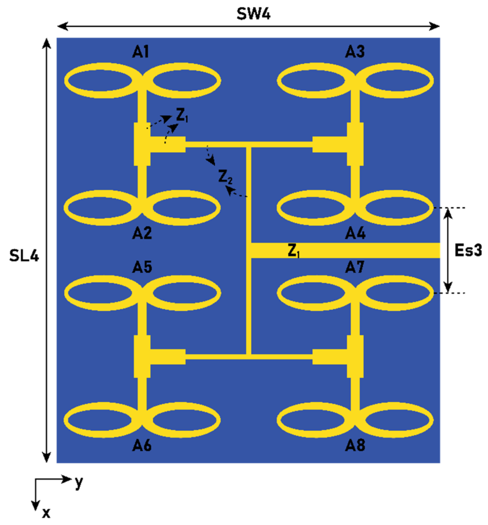
3.3. The 4 × 2 Array Antenna

This section proposes a final 4 × 2 array antenna (Ant4). It is to be noted that the interelement spacing between rows is not equal, and as a result, the pair of antennas generates a quad-beam. The proposed Ant4 is shown in Figure 13. The array factor (AF) for this particular case is as follows:
A F θ ,   φ = A F x θ ,   φ ·   A F y θ ,
where
A F x θ ,   φ = 1 + e j k E s 1 cos θ s i n ( φ ) + e j ( k E s 1 + E s 3 cos θ s i n ( φ ) + e j ( k 2 · E s 1 + E s 3 cos θ s i n ( φ )   and
A F y θ = 1 + e j k E s 2 s i n ( θ ) .
From the above equation, it is clear that the pair (A1, A2) and (A3, A4) causes the generation of the beam at θ 1 and φ 1 = 0 ° . Likewise, (A3, A4) and (A7, A8) generate a beam at θ 2 and φ 2 = 90 ° , while (A7, A8) and (A5, A6) lead to a beam at θ 3 and φ 3 = 180 ° . The fourth beam is due to (A1, A2) and (A5, A6) at θ 4 and φ 4 = 270 ° . At θ = 0 ° , the intensity of all quad beams is low, thus canceling the radiation pattern and generating a null with minor lobes. The estimated radiation pattern from the above equation is compared with the simulated pattern shown in Figure 14. Thus, Ant4 results in the dual-beam in the xz-plane at an angle of θ = ± 54 ° , with a half-power beamwidth (HPBW) of 31°. In the yz-plane, the dual-beam is achieved at an angle of θ = ± 58 ° , with an HPBW of 34°. Ant4 results in a high X-polarization of −24 dB in the xz-plane and −18 dB in the yz-plane, as shown in Figure 15. Ant4 achieves bandwidths ranging from 29.81–30.5 GHz, as illustrated in Figure 16a, with a peak gain of 10.3 dBi and an average total efficiency of 77%, as depicted in Figure 16b. It is worth noting that as the array antenna aperture increases, the bandwidth increases towards the lower frequency.

4. Results and Discussion
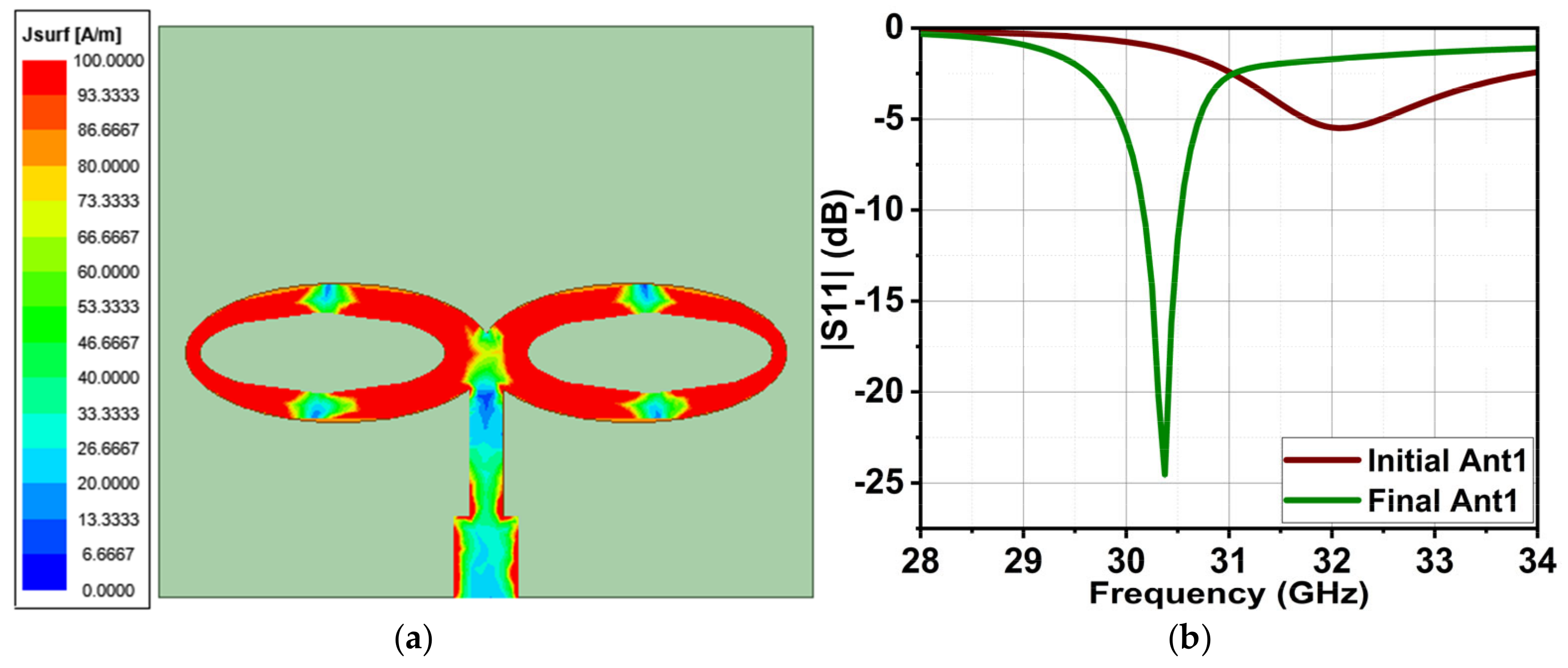
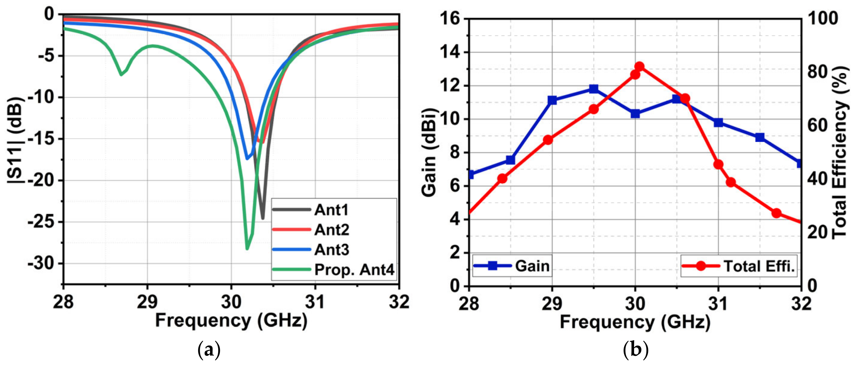
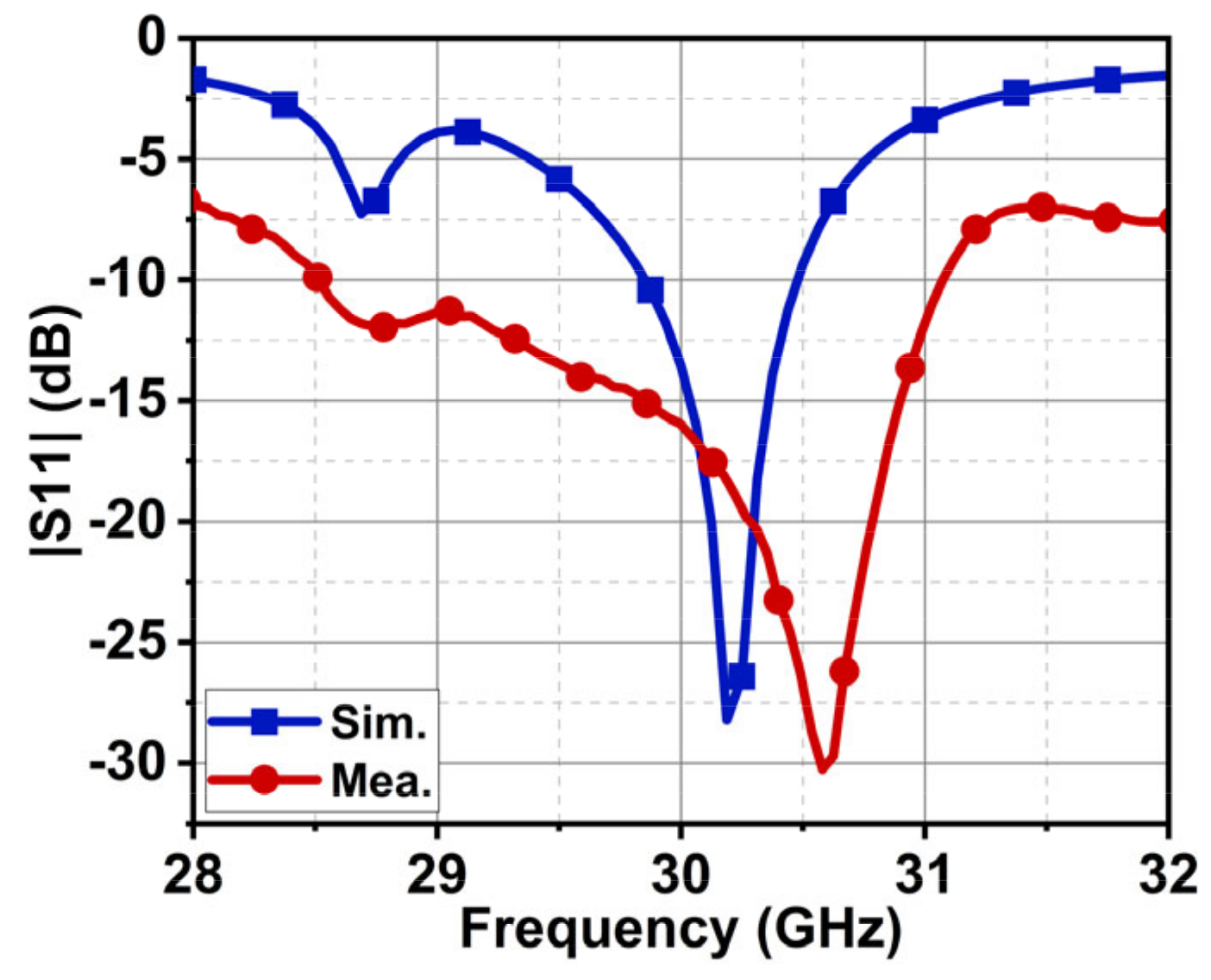
4.1. |S-Parameter|

The design of an array antenna begins with the development of a single-element structure (Ant1) which has compact dimensions of 0.71 λ 1 × 0.81 λ 1 . Initially, the antenna design resembles a circular patch, but this is modified into a dual-elliptical structure, which leads to an impedance mismatch. To address this, elliptical slots are etched within the structure, reducing the patch area but increasing the path of surface current to λ 1 . This adjustment generates a resonance at 30 GHz. The single-element antenna (Ant1) demonstrates a bandwidth ranging from 30.12 to 30.56 GHz and achieves a gain of 7.8 dBi.
The antenna’s performance is progressively enhanced by expanding Ant1 into a 4 × 2 array configuration (Ant4). The proposed array antenna exhibits a quad-beam behavior pattern through which a node device can simultaneously communicate with two other devices in the azimuthal plane and another two in the elevation plane. The distinctive beams forming at an angle of ±54° provide low interference between the communicating devices. However, in the process of achieving quad-beam, the antenna results in a slightly higher side-lobe level at ±15°, which could be reduced further by optimally increasing the spacing between the elements or by providing the distinctive phase and amplitude to form the constructive quad-beam with destructive patterns at the center. The spacing larger than optimal may result in undesired lobes, which distort an antenna’s performance.
To obtain a quad-beam, the Ant4 array features non-uniform element spacing along the x-axis, with 0.6 λ 1 spacing between both the first and second rows and the third and fourth rows, while the spacing between the second and third rows is reduced to 0.4 λ 1 . This non-uniform spacing separates the elongated beams observed in the previous 2 × 2 array (Ant3), and it results in dual beams in the xz-plane. In the y-axis, the spacing is maintained at one wavelength, which preserves the dual beams in the yz-plane like Ant3. The overall dimensions of Ant4 are 2.02 λ 1 × 1.82 λ 1 . The increase in radiating elements effectively expands the antenna aperture, thereby improving the gain.
The simulated results are validated through prototype fabrication. The fabricated antenna structure is shown in Figure 17a, with the measurement setup illustrated in Figure 17b. A comparison of the simulated and measured reflection coefficients (|S11|) indicates that the simulated bandwidth for |S11| ≥ 10 dB is 29.81–60.5 GHz, while the measured bandwidth is slightly broader, ranging from 28.5 to 31.1 GHz, as shown in Figure 18. The simulated resonance is at 30.2 GHz, while the measured resonance is at 30.5 GHz. The discrepancies in the simulated and measured results might be due to several factors. One such factor might be the use of an adopter to the interface vector network analyzer (VNA) to the antenna port because the used antenna port is a 2.4 mm SMA connector from Johnson, and its threading dimensions are different than the cable’s male connector. Also, other factors like fabrication tolerance and port soldering may have affected the antenna’s performance. Despite these differences, the bandwidth of simulated results falls under the measured results, with a shift in resonance of 0.5 GHz.

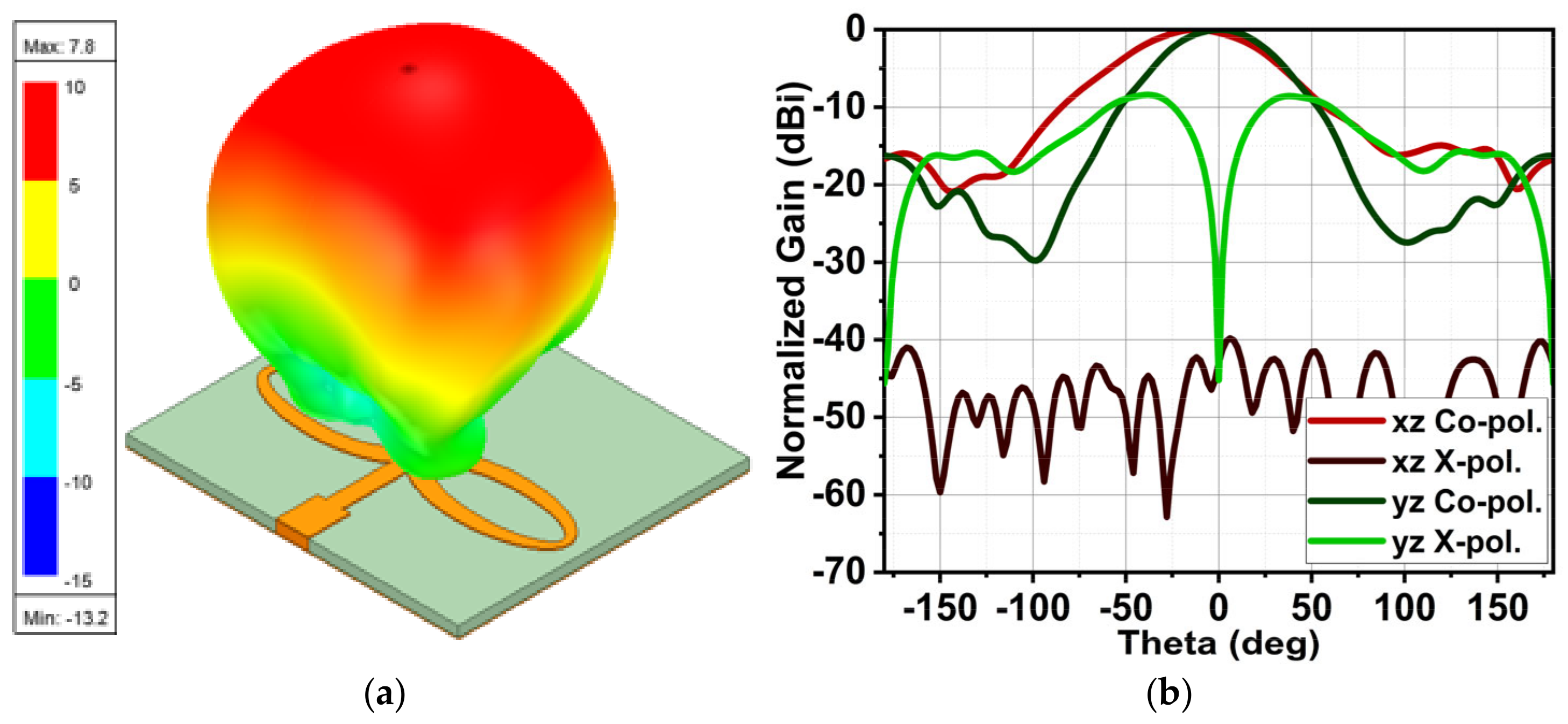
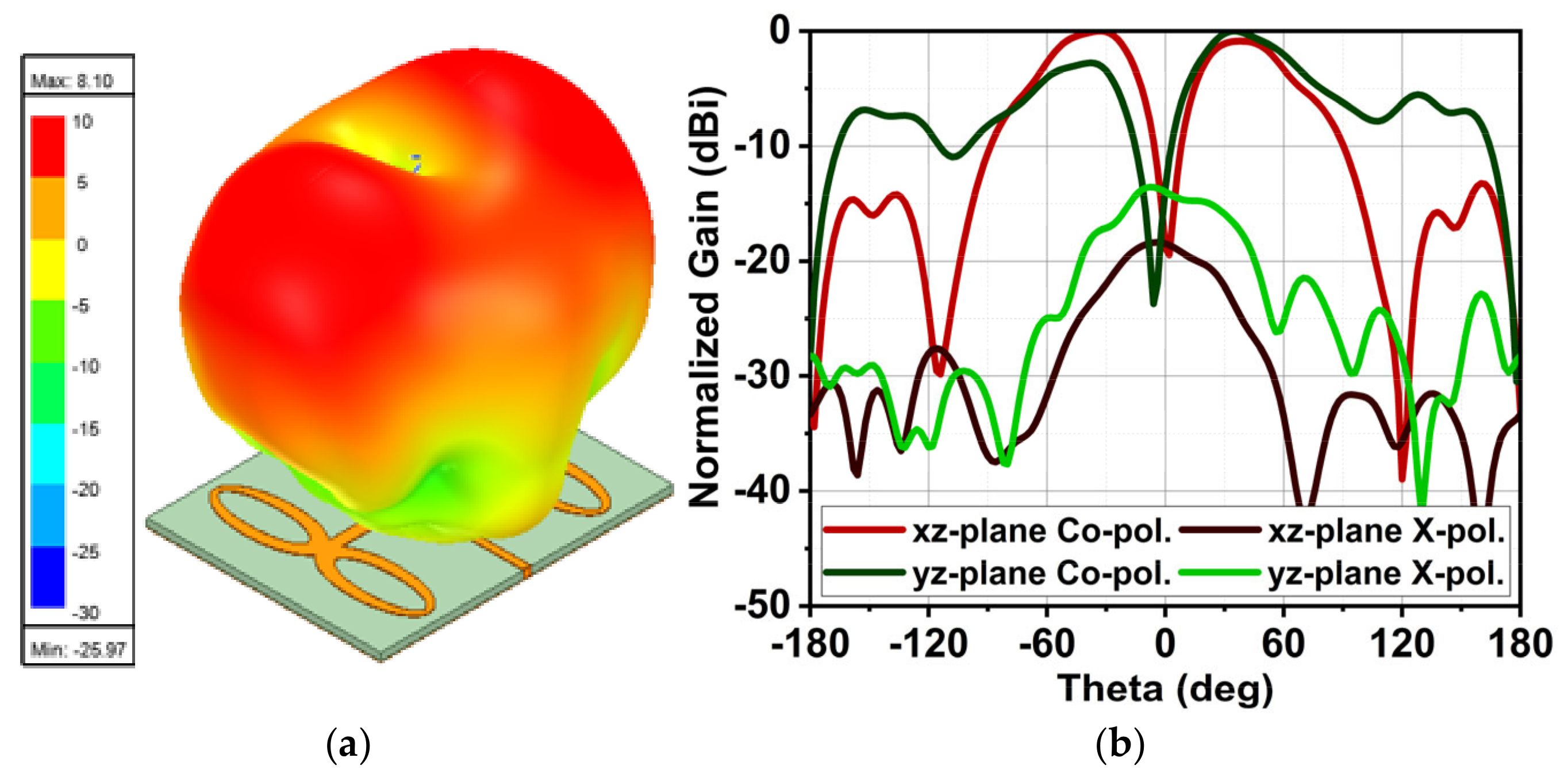
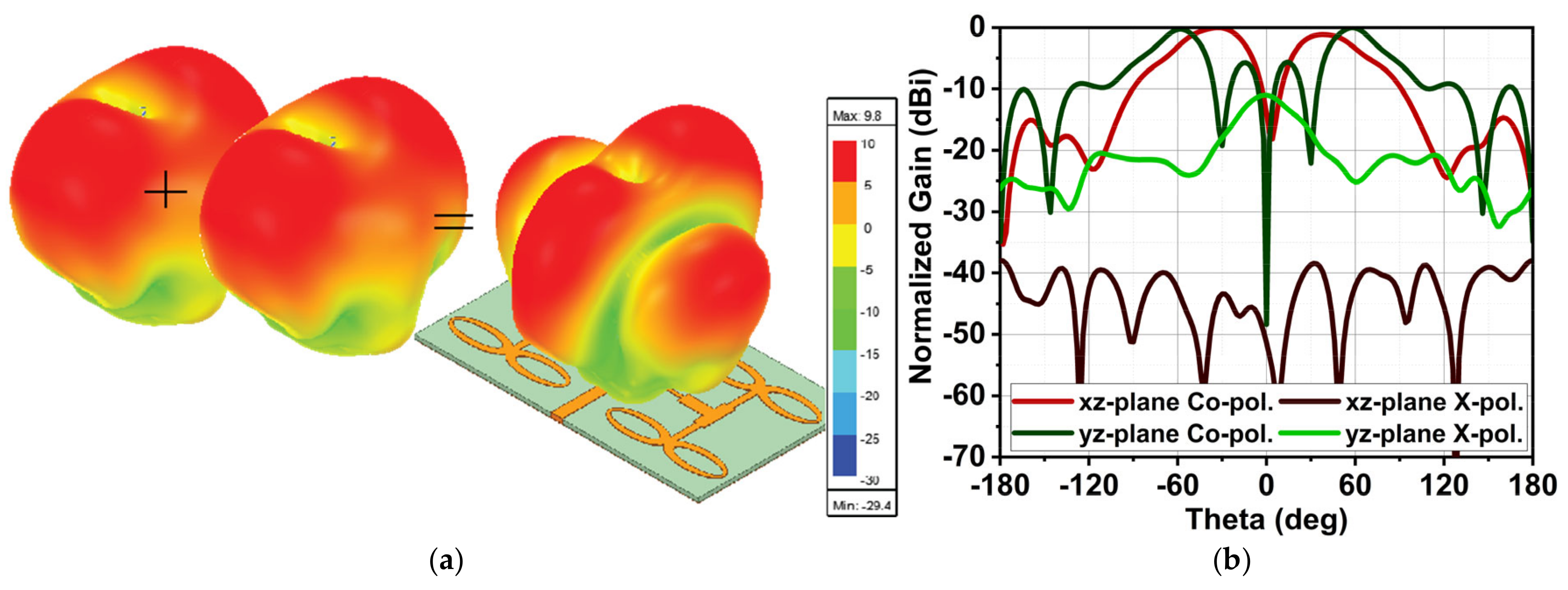
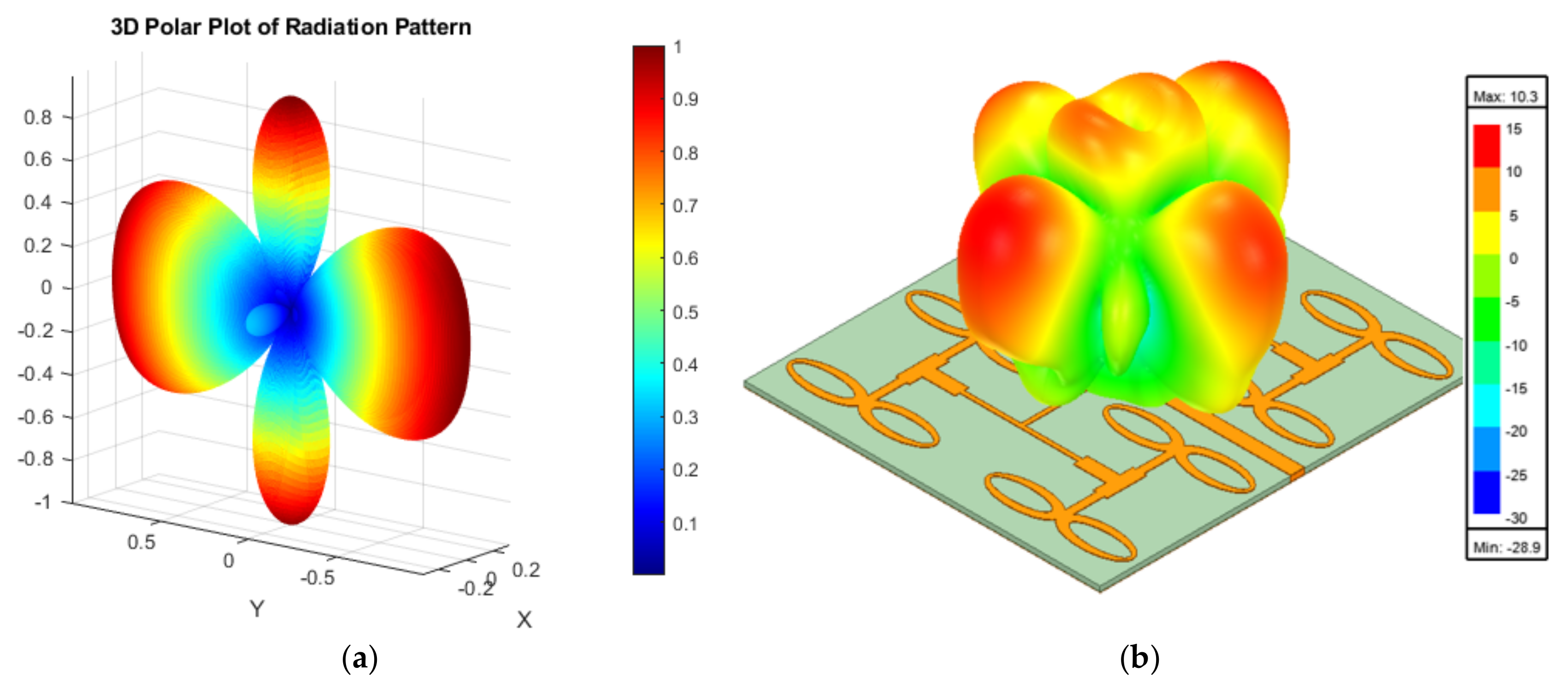
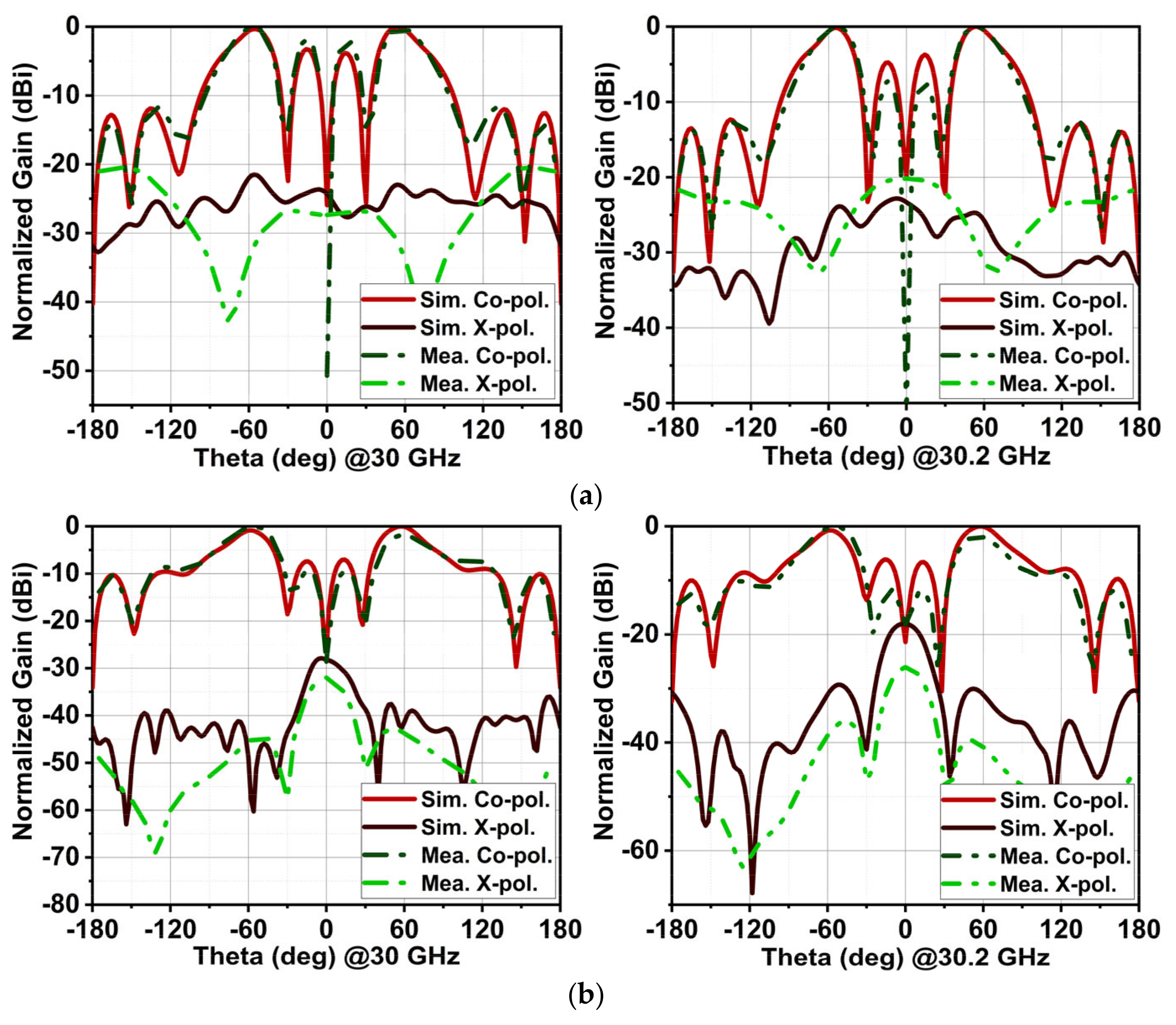
4.2. Radiation Pattern

The Ant4 antenna achieves a quad-beam in the broadside direction due to the non-uniform spacing, with two in the xz-plane and the other two in the yz-plane at an angle of θ = ± 54 ° . To provide a better perspective of the radiation pattern in the band of interest, it is shown at 30 GHz and 30.2 GHz in Figure 19. The simulated HPBW in the xz-plane is 33° and the measured HPBW is 30°, with an X-polarization of −21/−23 dB and −20/−20.2 dB, respectively. Likewise, in the yz-plane, the simulated HPBW is 31° and the measured HPBW is 35°, with an X-polarization of −28/−18 dB and −32/−26 dB, respectively. The simulated and measured gains of Ant4 in the band of interest are 10.3 dBi and 10.6 dBi, respectively, with the simulated average total efficiency of 77%, as depicted in Figure 20.

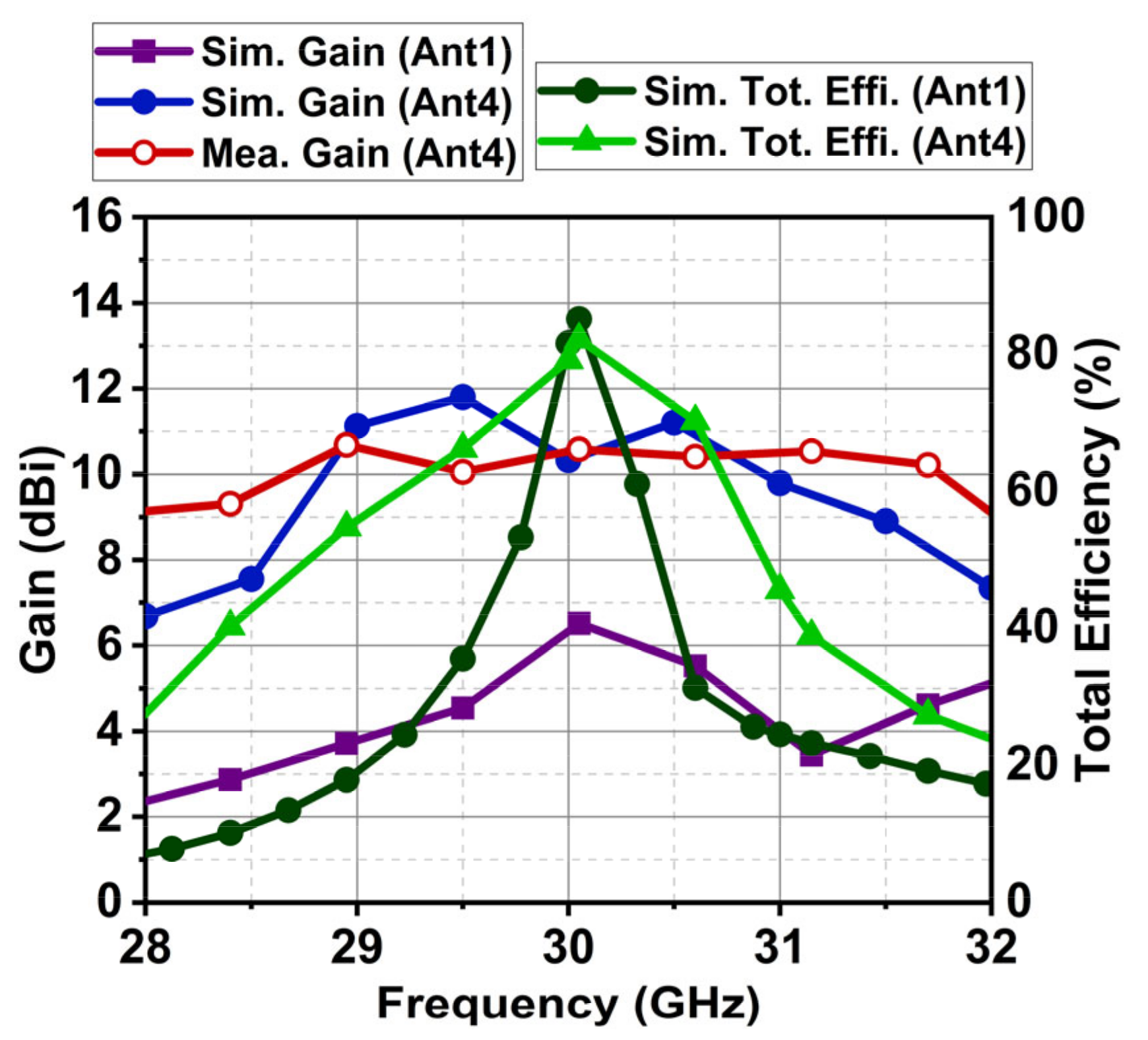
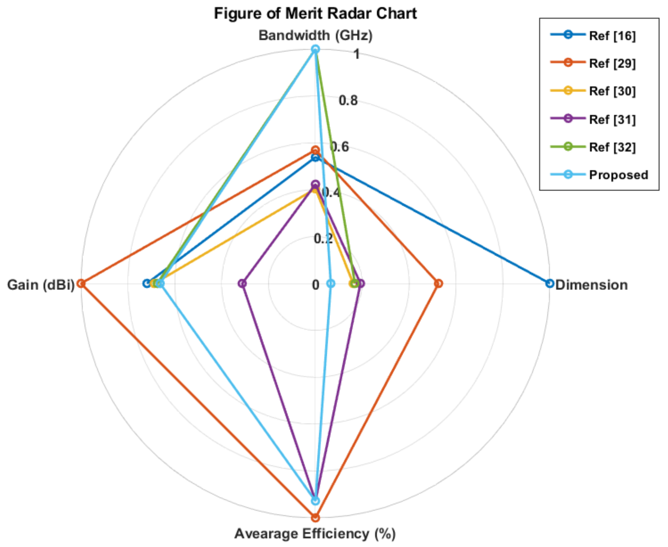
4.3. Performance Comparison

The proposed Ant4 antenna is compared with existing designs, as summarized in Table 1. While multilayer structures, such as rectangular waveguides with patches [26] and magneto-electric (ME) dipole antennas [27], demonstrate superior performance in bandwidth, gain, and directivity, these designs come with significant complexity. However, multilayer antennas are challenging to manufacture due to alignment issues between the layers, where even slight mismatches can result in substantial performance degradation.
In contrast, planar structures [28,29,30,31,32] offer simplicity in both fabrication and integration while still providing a satisfactory performance for practical applications. Among these, the proposed Ant4 antenna achieves better directivity than all other planar structures listed, with particularly strong X-polarization control in both the xz- and yz-planes. Additionally, the bandwidth performance of the Ant4 antenna (28.5–31.1 GHz) surpasses that of other designs, such as those in [29,30,31]. The gain of the proposed antenna (10.6 dBi) is also competitive with the other designs, ensuring a robust performance. Consequently, the performance of the proposed Ant4 with other planar arrays (ignoring the multilayer structures) is illustrated in Figure 21 through a figure-of-merit plot for a better perspective and improved comprehension.
Overall, the proposed antenna strikes a balance between performance and structural simplicity, making it well-suited for 5G wireless applications that require high-gain, multi-beam coverage. Its compact size, scalability, and efficient quad-beam radiation pattern position it as an attractive alternative to more complex multilayer or waveguide-based designs.

5. Conclusions

The article presents the design of a compact 4 × 2 array antenna with dimensions of 2.02 λ 1 × 1.82 λ 1 for 5G millimeter-wave applications. The proposed antenna achieved a quad-beam radiation pattern through the innovative use of non-uniform element spacing. A detailed progression was provided, beginning from the analysis of a single-element antenna and scaling up to the final 4 × 2 array configuration. The non-uniform inter-element spacing of greater than 0.5 λ 1 was identified as the primary factor enabling the formation of the quad-beam pattern. This unique configuration resulted in two beams in the xz-plane and two beams in the yz-plane, improving the coverage and beam steering capabilities in the azimuthal and elevation planes, which are essential for modern 5G communication networks.
The innovation in this work lies in the antenna’s ability to achieve complex multi-beam radiation using a simple planar structure and a parallel feed technique. The design maintains structural simplicity and reduces the fabrication challenges often associated with multilayer or waveguide-based antenna systems. By optimizing the element spacing and tuning the feed network, the antenna effectively mitigates mutual coupling and radiation nulls, ensuring a stable performance with a peak gain of 10.6 dBi and a bandwidth spanning 28.5–31.1 GHz. Furthermore, the design is scalable, with gain improvements demonstrated through aperture replication.
These advancements make the proposed antenna highly suitable for 5G wireless applications where multi-beam coverage, high gain, and compact size are critical performance factors. Compared to existing designs, this antenna offers a balanced trade-off between performance and complexity, achieving better or comparable directivity, bandwidth, and polarization characteristics without the need for intricate feed structures or multiple layers.

Author Contributions

Conceptualization, P.S.B.G. and T.A.; methodology, P.S.B.G.; software, P.S.B.G., S.P. and B.S.V.; validation, P.S.B.G., S.P.G., J.A. and P.M.P.; formal analysis, P.S.B.G., P.R.M. and T.A.; writing—original draft preparation, P.S.B.G.; writing—review and editing, T.A., P.R.M. and B.S.V.; visualization, S.P. and P.M.P.; supervision, T.A. All authors have read and agreed to the published version of the manuscript.

Funding

This research received no external funding.

Data Availability Statement

The data are available in the manuscript in the form of results.

Conflicts of Interest

Author Jaume Anguera was employed by the company Ignion. The remaining authors declare that the research was conducted in the absence of any commercial or financial relationships that could be construed as a potential conflict of interest.

References

  1. Chen, J.; Zhang, D.; Wu, Z.; Zhou, F.; Sun, Q.; Chen, Y. Contactless Electrocardiogram Monitoring With Millimeter Wave Radar. IEEE Trans. Mob. Comput. 2024, 23, 270–285. [Google Scholar] [CrossRef]
  2. Venon, A.; Dupuis, Y.; Vasseur, P.; Merriaux, P. Millimeter Wave FMCW RADARs for Perception, Recognition and Localization in Automotive Applications: A Survey. IEEE Trans. Intell. Veh. 2022, 7, 533–555. [Google Scholar] [CrossRef]
  3. Harlow, K.; Jang, H.; Barfoot, T.D.; Kim, A.; Heckman, C. A New Wave in Robotics: Survey on Recent MmWave Radar Applications in Robotics. IEEE Trans. Robot. 2024, 40, 4544–4560. [Google Scholar] [CrossRef]
  4. Shariff, B.G.P.; Ali, T.; Mane, P.R.; Kumar, P. Array Antennas for mmWave Applications: A Comprehensive Review. IEEE Access 2022, 10, 126728–126766. [Google Scholar] [CrossRef]
  5. Magray, M.I.; Su, S.-W.; Tarng, J.-H. Differential-Fed, Dual-Aperture Based, Quasi-End-Fire 5G mmWave Antenna-in-Package Design. IEEE Access 2022, 10, 89091–89100. [Google Scholar] [CrossRef]
  6. Zheng, D.; Wu, G.-B.; Wang, D.; Chan, K.F.; Wu, K.; Chan, C.H. Planar Leaky-Wave Antenna Featuring Wideband Fixed-Beam Radiation and Tailorable Directional Angle for Millimeter-Wave Applications. IEEE Trans. Antennas Propag. 2023, 71, 3238–3250. [Google Scholar] [CrossRef]
  7. Chen, Y.; Zhang, L.; He, Y.; Mao, C.; Gao, S.S. A Low-Cost, Quad-Beam, Dual-Polarized, 2-D Leaky Wave Antenna With Wide-Angle Beam Scanning for Millimeter-Wave Applications. IEEE Trans. Antennas Propag. 2023, 71, 7342–7353. [Google Scholar] [CrossRef]
  8. Muhammad, A.; Khan, M.U.; Malfajani, R.S.; Sharawi, M.S.; Alathbah, M. An Integrated DRA-Based Large Frequency Ratio Antenna System Consisting of a MM-Wave Array and a MIMO Antenna for 5G Applications. IEEE Open J. Antennas Propag. 2024, 5, 368–378. [Google Scholar] [CrossRef]
  9. Huang, K.; Zhang, Y. Analysis and Design of Dual-Polarized Millimeter-Wave Filtering Magneto-Electric Dipole Antenna. IEEE Trans. Antennas Propag. 2023, 71, 6947–6952. [Google Scholar] [CrossRef]
  10. Mane, P.R.; Kumar, P.; Ali, T.; Alsath, M.G.N. Planar MIMO antenna for mmWave applications: Evolution, present status & future scope. Heliyon 2023, 9, e13362. [Google Scholar] [CrossRef]
  11. Parveez Shariff, B.G.; Ali, T.; Mane, P.R.; Kumar, P.; Kumar, P.A. Compact Petal Shaped Two-Port MIMO Antenna for Quad-Band Millimeter Wave 5G Applications. In Proceedings of the 2023 International Telecommunications Conference (ITC-Egypt), Alexandria, Egypt, 18–20 July 2023; pp. 1–6. [Google Scholar]
  12. Bhadrvathi Ghouse, P.S.; Mane, P.R.; Thankappan Sumangala, S.; Kumar Puttur, V.; Pathan, S.; Jhunjhunwala, V.K.; Ali, T. A Compact Dual-Band Millimeter Wave Antenna for Smartwatch and IoT Applications with Link Budget Estimation. Sensors 2023, 24, 103. [Google Scholar] [CrossRef]
  13. Zheng, W.; Wang, J.; Du, H. A Broadband Quad-Beam Patched Leaky-Wave Antenna Based on Substrate Integrated Coaxial Line for Multi-Beam Applications. IEEE Antennas Wirel. Propag. Lett. 2024, 23, 4748–4752. [Google Scholar] [CrossRef]
  14. Xu, H.; Wei, P.; Jiang, S.; Yu, Z.; Zhou, J.; Liu, C. Wideband Circularly Polarized Planar U-Shaped Antenna Array for Millimeter-Wave Applications. IEEE Trans. Antennas Propag. 2023, 71, 6971–6976. [Google Scholar] [CrossRef]
  15. Siddiqui, Z.; Sonkki, M.; Rasilainen, K.; Chen, J.; Berg, M.; Leinonen, M.E.; Pärssinen, A. Dual-Band Dual-Polarized Planar Antenna for 5G Millimeter-Wave Antenna-in-Package Applications. IEEE Trans. Antennas Propag. 2023, 71, 2908–2921. [Google Scholar] [CrossRef]
  16. Duddu, S.K.; Kumar, J. High-Gain Series-Fed-Planar Millimetre-Wave Franklin Antenna Array. Arab. J. Sci. Eng. 2024, 49, 6331–6341. [Google Scholar] [CrossRef]
  17. David Joseph, S.; Ball, E.A. Series-Fed Millimeter-Wave Antenna Array Based on Microstrip Line Structure. IEEE Open J. Antennas Propag. 2023, 4, 254–261. [Google Scholar] [CrossRef]
  18. Prasad, S.; Meenakshi, M.; Adhithiya, N.; Rao, P.H.; Krishna Ganti, R.; Bhaumik, S. mmWave multibeam phased array antenna for 5G applications. J. Electromagn. Waves Appl. 2021, 35, 1802–1814. [Google Scholar] [CrossRef]
  19. Zhang, Y.; Han, Z.; Tang, S.; Shen, S.; Chiu, C.-Y.; Murch, R. A Highly Pattern-Reconfigurable Planar Antenna With 360° Single- and Multi-Beam Steering. IEEE Trans. Antennas Propag. 2022, 70, 6490–6504. [Google Scholar] [CrossRef]
  20. Wan, Y.; Liao, S.; Wang, Y.; Li, L.; Wei, J.; Che, W.; Xue, Q. From Curved to Planar: Enabling Large-Spacing Phased Array Antenna to Achieve Grating-Lobe-Free Wide-Angle Scanning. IEEE Trans. Antennas Propag. 2025, 1. [Google Scholar] [CrossRef]
  21. Li, P.; Liang, J.; Chen, X. Study of Printed Elliptical/Circular Slot Antennas for Ultrawideband Applications. IEEE Trans. Antennas Propag. 2006, 54, 1670–1675. [Google Scholar] [CrossRef]
  22. Khabba, A.; Wakrim, L.; Ibnyaich, S.; Hassani, M.M. Beam-Steerable Ultra-Wide-Band Miniaturized Elliptical Phased Array Antenna Using Inverted-L-Shaped Modified Inset Feed and Defected Ground Structure for 5G Smartphones Millimeter-Wave Applications. Wirel. Pers. Commun. 2022, 125, 3801–3833. [Google Scholar] [CrossRef]
  23. Balanis, C.A. Antenna theory: Analysis and Design, 4th ed.; Wiley: Hoboken, NJ, USA, 2016; ISBN 978-1-118-64206-1. [Google Scholar]
  24. Beckers, M.; Weise, B.; Kalapis, S.; Gries, T.; Seide, G.; Bunge, C.-A. Basics of light guidance. In Polymer Optical Fibres; Elsevier: Amsterdam, The Netherlands, 2017; pp. 9–46. ISBN 978-0-08-100039-7. [Google Scholar]
  25. Baumgartner, P.; Masiero, A.; Riener, C.; Bauernfeind, T. Simulation Based Poynting Vector Description of the Field Regions for Simple Radiating Structures. Electronics 2022, 11, 1967. [Google Scholar] [CrossRef]
  26. Herranz-Herruzo, J.I.; Ferrando-Rocher, M.; Valero-Nogueira, A.; Bernardo-Clemente, B. Wideband Circularly Polarized mm-Wave Array Antenna Using H-Shaped Low-Axial-Ratio Apertures. IEEE Trans. Antennas Propag. 2023, 71, 4564–4569. [Google Scholar] [CrossRef]
  27. Xiang, L.; Wu, F.; Chen, K.; Zhao, R.; Ma, S.; Zhu, Y.; Yu, C.; Jiang, Z.H.; Yao, Y.; Hong, W. Wideband Single and Dual Linearly Polarized Magneto-Electric Dipole Array Antennas for 5G/6G Millimeter-Wave Applications. IEEE Open J. Antennas Propag. 2024, 5, 525–539. [Google Scholar] [CrossRef]
  28. Alharbi, A.G.; Rahman, H.M.A.; Khan, M.M.; Abbasi, M.I.; Albraikan, A.A.; Almalki, F.A. Design and Study of a Miniaturized Millimeter Wave Array Antenna for Wireless Body Area Network. Int. J. Antennas Propag. 2022, 2022, 1736377. [Google Scholar] [CrossRef]
  29. Malviya, L.; Gupta, P. Millimeter Wave High-Gain Antenna Array for Wireless Applications. IETE J. Res. 2021, 69, 2645–2654. [Google Scholar] [CrossRef]
  30. Ghosh, S.; Baghel, G.S.; Swati, M.V. A low-profile, high gain, dual-port, planar array antenna for mm-wave powered 5G IoT systems. AEU—Int. J. Electron. Commun. 2022, 155, 154354. [Google Scholar] [CrossRef]
  31. Sufian, M.A.; Hussain, N.; Choi, D.; Lee, S.-M.; Gil, S.-K.; Kim, N. High gain quasi-omnidirectional dipole array fed by radial power divider for millimeter-wave IoT sensing. Sci. Rep. 2024, 14, 16279. [Google Scholar] [CrossRef]
  32. Tariq, S.; Rahim, A.A.; Sethi, W.T.; Faisal, F.; Djerafi, T. Metasurface based antenna array with improved performance for millimeter wave applications. AEU—Int. J. Electron. Commun. 2024, 177, 155195. [Google Scholar] [CrossRef]
Figure 1. Initial design of the antenna (Ant1) (a), and its surface current representation (b).
Electronics 14 01056 g001
Figure 2. Final design of the single-element antenna (Ant1). The dimensions in mm are: EL = 7.3, Eh1 = 3.74, Ev1 = 1.7, Eh2 = 3, Ev2 = 1, Fl1 = 1.8, Fw1 = 0.4, Fl2 = 1, Fw2 = 0.78, SW1 = 8, and SL1 = 7.
Electronics 14 01056 g002
Figure 3. Surface current distribution of the final single-element antenna (Ant1) in (a), and (b) represents its reflection coefficient of a comparison of the initial elliptical antenna and the final elliptical ring (figure-eight) antenna.
Electronics 14 01056 g003
Figure 4. (a) The 3D radiation pattern and peak gain of Ant1, and (b) a 2D representation with co- and X-polarization in the xz- and yz-planes.
Electronics 14 01056 g004
Figure 5. A Poynting vector representation of Ant1.
Electronics 14 01056 g005
Figure 6. Modeling of the single-element antenna with the transmission line theory.
Electronics 14 01056 g006
Figure 7. (a) Comparison of the reflection coefficient |S11| obtained from the electromagnetic solver and the circuit simulator. (b) The impedance comparison of the numerical method, electromagnetic solver, and circuit simulator.
Electronics 14 01056 g007
Figure 8. Effect on the reflection coefficient of the single-element antenna from the variations in the major (Eh1) and minor (Ev1) axes of an elliptical patch in (a) and (b), respectively. Likewise, the variations in the resonance frequency are due to variations in the major (Eh2) and minor (Ev2) axes of the elliptical slot in (c) and (d), respectively.
Electronics 14 01056 g008
Figure 9. (a) The 2 × 1 array antenna (Ant2) with elements separated by a distance of Es1 = 6 mm, where SW2 = 8 mm and SL2 = 10 mm. (b) A pictorial representation of the wave formation by the 2 × 1 Ant2 due to the Es1 spacing.
Electronics 14 01056 g009
Figure 10. (a) The resulting 3D radiation pattern of Ant2. (b) A 2D representation of the 2 × 1 array (Ant2) antenna.
Electronics 14 01056 g010
Figure 11. The 2 × 2 array (Ant3) with Es1 = 6 mm, Es2 = 10 mm, SW3 = 18 mm, and SL3 = 10 mm.
Electronics 14 01056 g011
Figure 12. A demonstration of the 3D radiation pattern formation of Ant3 (a) and its respective 2D pattern (b).
Electronics 14 01056 g012
Figure 13. The proposed 4 × 2 array antenna (Ant4), with Es3 = 4 mm, SL4 = 20 mm, and SW4 = 18 mm.
Electronics 14 01056 g013
Figure 14. Comparison of the 3D radiation obtained from (a) the equation, and (b) the simulated radiation pattern from Ant4 at 30.2 GHz.
Electronics 14 01056 g014
Figure 15. The simulated radiation pattern of Ant4 representing the co- and X-polarizations in (a) xz-plane and (b) yz-plane.
Electronics 14 01056 g015
Figure 16. (a) A comparison of the proposed Ant4 reflection coefficient |S11| with its previous antenna structures. (b) The simulated gain and total efficiency of Ant4.
Electronics 14 01056 g016
Figure 17. (a) Prototype fabrication of the Ant4 antenna. (b) Measurement setup of the |S-parameter| and radiation pattern in the anechoic chamber.
Electronics 14 01056 g017
Figure 18. The simulated and measured reflection coefficient |S11| of the proposed Ant4 antenna.
Electronics 14 01056 g018
Figure 19. The simulated and measured radiation patterns of Ant4 at 30 GHz and 30.2 GHz. (a) Pattern in the xz-plane and (b) in the yz-plane.
Electronics 14 01056 g019
Figure 20. Plot of the gain and total efficiency of Ant1 compared with Ant4.
Electronics 14 01056 g020
Figure 21. Figure-of-merit plot comparing the proposed antenna Ant4 performance with other planar arrays.
Electronics 14 01056 g021
Table 1. Comparison of the proposed array antenna with state-of-the-art designs.
Ref. Dim   in   λ 3 Res. GHzDesign TechniqueArray Conf.BW in GHzHPBW in xz-Plane (deg)X-pol. in xz-Plane (dB)HPBW in yz-Plane (deg)X-pol. in yz-Plane (deg)Gain (dBi)Avg. Tot. Effi. (%)
[16] 1.96 × 3.74 × 0.15 28Planar array with hybrid feeding 2 × 6 27–28.457°NAV20°NAV11.5NAV
[26] 4.2 × 4.2 × 1.93 28Multilayer with a groove-gap waveguide 2 × 2 26.9–33.116°NAV16°NAV22NAV
[27] 5 × 3 × 0.017 30Magneto-electric dipole with parallel feed 4 × 4 19–5117°−2016°181882
[28] 7.25 × 4.3 × 0.07 60Planar array with parallel feed 1 × 4 50–6565°NAVOmni.NAV5.3765.5
[29] 4.8 × 1.72 × 0.07 28Planar array with hybrid feed 6 × 2 27.06–28.5458°NAVOmni.NAV1683
[30] 1.64 × 3.6 × 0.03 28Planar array with parallel feed 2 × 4 27.75–28.854°NAV20°NAV11NAV
[31] 10.55 × 0.02   * Planar dipole array828–29.1Omni.NAVOmni.NAV577
[32] 1.93 × 1.92 × 0.05 28Planar array with parallel feed 1 × 2 28–32.560°NAV30°NAV10.8NAV
Prop. 2 × 1.8 × 0.02 30Planar array with parallel feed 4 × 2 28.5–31.130°−20.235°−2610.677
Note: Array Conf., array configuration; NAV, not available, The dimension of [31] with * is circular structure.
Disclaimer/Publisher’s Note: The statements, opinions and data contained in all publications are solely those of the individual author(s) and contributor(s) and not of MDPI and/or the editor(s). MDPI and/or the editor(s) disclaim responsibility for any injury to people or property resulting from any ideas, methods, instructions or products referred to in the content.

