1. Introduction
Image processing techniques have been used extensively in many different applications, such as medical diagnosis [
1,
2,
3,
4], intelligent driving [
5,
6,
7,
8], and target identification [
9,
10,
11]. Digital image convolution is one of the most fundamental processing techniques for extracting image features [
12,
13,
14,
15]. This convolution process involves multiplying the image pixel matrix with a kernel, encompassing numerous parallel multiply-accumulate (MAC) operations. The increasing demand for real-time and high-quality image processing has sparked a rapid expansion in custom hardware designed to accelerate MAC operations. Diverse electronic computing hardware, encompassing field-programmable gate arrays (FPGAs) and graphics processing units (GPUs), have been developed to enhance computational capabilities. Meanwhile, various fast and efficient computing technologies have also been developed, such as reversible computing [
16] and neuromorphic computing [
17]. However, against the backdrop of gradual failure of Moore’s law [
18], these electronic schemes still encounter bottlenecks in terms of speed and energy efficiency. The enhancement of computing speed heavily depends on the scaling up of hardware, resulting in an annual surge in data center costs and power consumption. However, even this expansion fails to keep pace with the explosive development of technologies such as artificial intelligence, cloud computing, and big data. Furthermore, a multitude of small- and medium-sized unmanned platforms, including drones and robots, hindered by their restricted payload capacities, cannot accommodate bulky computing hardware, thereby generating an imperative need for solutions that offer high computing power with low power consumption. In recent years, photonic computation, which employs photons as the information carrier instead of electrons, has been rapidly developed due to its numerous advantages, including intrinsically large bandwidth, low latency, and high parallelism. Although a prototype made up of discrete devices was demonstrated decades ago [
19], it remained excessively bulky and unstable. To address these limitations, photonic integration technology [
20,
21,
22] was introduced, offering compactness, scalability, and cost-effectiveness. In 2007, Shen et al. pioneered the concept of a coherent nanophotonic chip using Mach-Zehnder interferometer (MZI) meshes for vowel recognition [
23], which opened a new era of integrated photonic computation. Since then, various integrated photonic computing chips have been extensively reported, primarily categorized into two groups: those utilizing MZI meshes [
24,
25,
26,
27] and those employing micro-ring (MRR) meshes [
28,
29,
30]. The former typically utilizes a single coherent light source and carries out MAC operations through light interference within the MZI meshes, while the latter employs multiple light sources with varying wavelengths, modulated by MRRs operating in distinct states, for loading weights during MAC operations. Both types of integrated photonic computing chips possess their own advantages and are widely studied. In this paper, taking into account the consumption of light sources, we opted for the cascaded MZIs configuration and presented a scalable silicon-based photonic computing processor capable of executing digital image convolution. The proposed chip, measuring 1.5 mm × 6 mm, is comprised of 20 MZIs and capable of executing arbitrary matrix transformations with a dimension of 4 × 4. Along with the off-chip laser source, photodetector (PD) arrays, and upper computer, a digital image convolution experiment platform is constructed based on the packaged photonic computing chip. A self-configuring algorithm based on gradient descent method is utilized for weight training to load convolution kernel. The proposed chip is characterized by comparing with a 64-bit computer in performing convolution for a digital image with a resolution of 320 × 256, and the relative computation error is less than 2.3%. Under plausible assumptions, notably the integration of cutting-edge photonic I/O technology and the realization of substantially larger chip dimensions, the proposed processor promises remarkable enhancements in both computing speed and energy efficiency, potentially achieving improvements spanning one to two orders of magnitude when compared to current top-tier electronic computing devices, such as NVIDIA’s AI computing cards.
2. Device Design and Experimental Setup
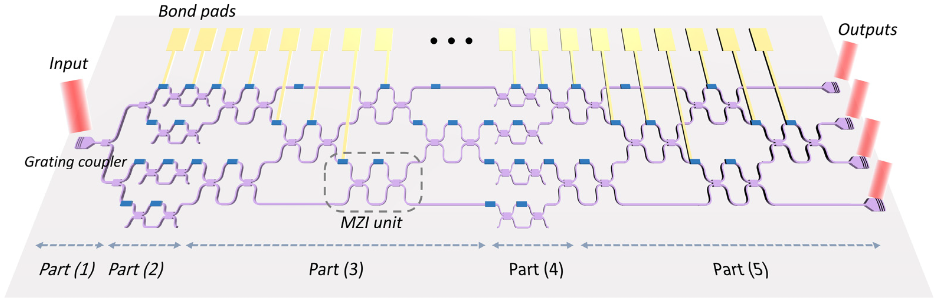
The schematic of the photonic computing chip demonstrated in this work is shown in
Figure 1. The chip consists of five parts. Part (1) is a 1-to-4 power splitter, and Part (2) is composed of four parallel MZIs, which connect to the respective outputs of the power splitter. These MZIs are used to load the input signals by modulating the light intensity. Parts (3), (4), and (5) are all MZI arrays, which can perform an arbitrary matrix transformation as a whole according to singular value decomposition [
31]. Specifically, Parts (3) and (5) are the same and are composed of six MZIs, respectively, which are arranged as a rectangular mesh, as reported in Ref. [
29]. These two parts can perform arbitrary unitary matrix transformation. Part (4) has 4 MZIs used for intensity attenuation, achieving arbitrary diagonal matrix transformation. The rectangular scheme, rather than the triangular scheme [
32] designed by Reck, is chosen in order to halve the optical depth, which is important for minimizing transmission loss and reducing chip size. Besides, the rectangular scheme has a natural symmetry that makes it significantly more robust to fabrication errors [
31]. In general, the chip contains 20 MZIs and 40 phase shifters in total.
The external light is firstly coupled into the photonic computing chip through a grating coupler, subsequently divided into four equal beams by Part (1). Following transmission through Part (2), all of them undergo modulation with corresponding electrical signals, subsequently being mixed within the MZI network encompassing Parts (3), (4), and (5), which performs MAC operations in the optical domain through splitting and interference. Eventually, the four mixed light beams are coupled out of the chip via grating couplers and captured by four commercial photodetectors. The aforementioned process is capable of executing matrix-vector multiplication, represented by the equation X·B = A. In this equation, B denotes a four-dimensional vector determined by the input electrical signals transmitted to Part (2), X represents the matrix transformation carried out by the MZI network, and A signifies another four-dimensional vector that is determined by the output signals collected by the photodetectors.
The photonic computing chip has been crafted on the silicon-on-insulator (SOI) platform, featuring a top Si layer of 220 nm and SiO
2 cladding of 2 μm. The grating coupler employed is of the focused type [
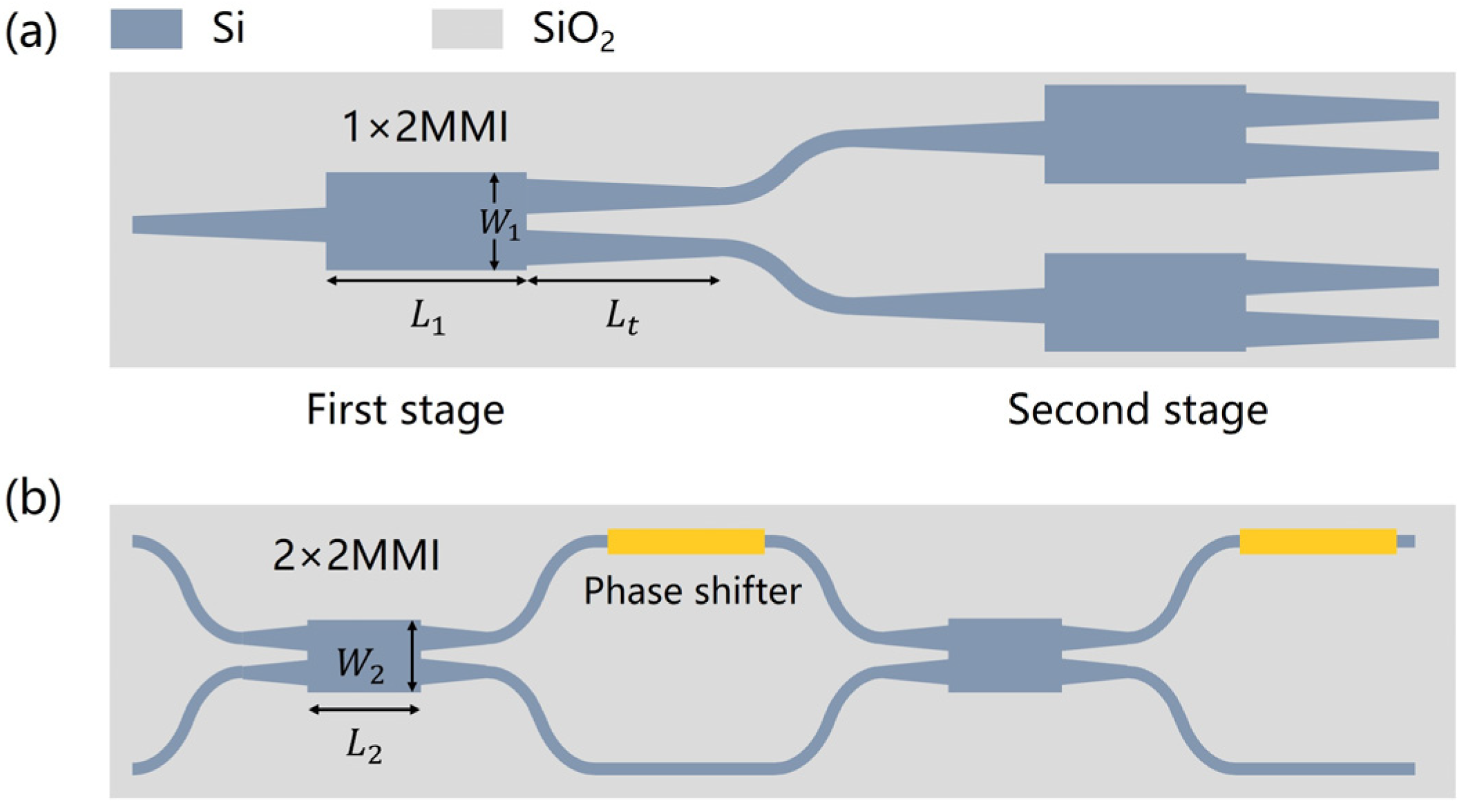
31], with a shallow etch depth of 150 nm. The grating’s period and duty cycle are designed at 650 nm and 0.5, respectively, optimized for a center wavelength of 1550 nm. The power splitter in Part (1) is comprised of three cascaded 1 × 2 multimode interference (MMI) couplers, with detailed structures depicted in
Figure 2a. The first MMI stage divides the incident light into two equal parts, and, subsequently, the second MMI stage further divides this light into four equal components. The dimensions of the multimode waveguide are specified as
L1 = 7.9 μm in length and
W1 = 3.2 μm in width. To mitigate abrupt width transitions and minimize reflection losses at the junctions between single-mode and multimode waveguides, tapered structures with a length of
Lt = 10 μm are introduced. We employ a light source with a wavelength of 1550 nm and a power of 10.6 dBm as the input for the beam splitter, resulting in optical powers of approximately 4.3 dBm, 4.2 dBm, 4.2 dBm, and 4.2 dBm at its four output terminals, respectively. Consequently, the beam splitter exhibits an excess loss of approximately 0.4 dB.
The MZI serves as the fundamental building block of the photonic computing chip, consisting of two 3-dB couplers and two phase shifters, as depicted in
Figure 2b. The 3-dB coupler employs a 2 × 2 MMI configuration, featuring dimensions of
L2 = 31 μm in length and
W2 = 5.2 μm in width. The phase shifter, utilizing the thermal-optic effect, is achieved by depositing a 0.1 μm-thick layer of TiN film above the waveguide, serving as a thermal resistance. The TiN film is designed to exhibit a resistance of 480 Ω, with dimensions of 100 μm × 2.5 μm.
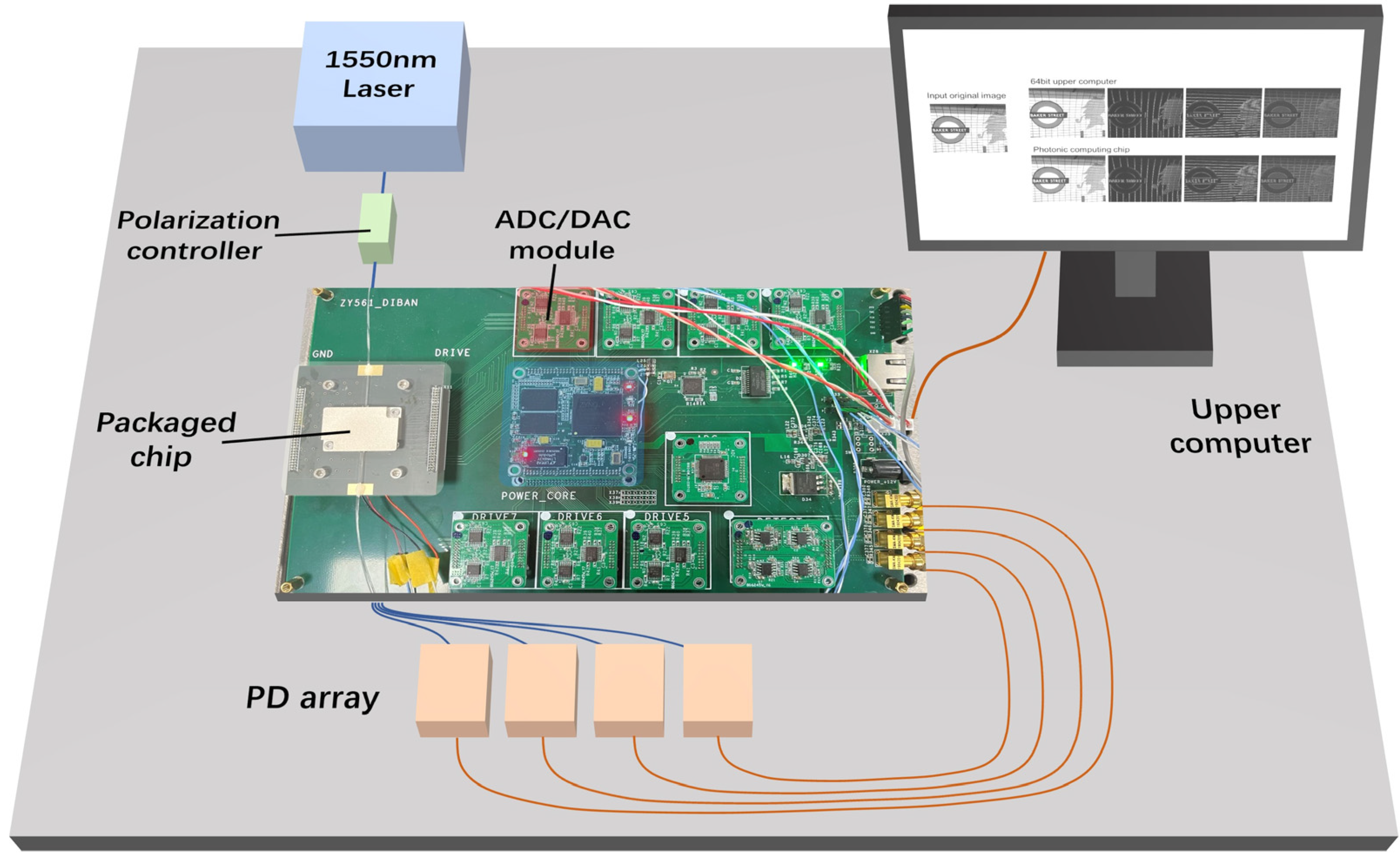
To drive the proposed photonic computing processor, a custom-designed control circuit has been developed, utilizing six 8-channel digital-to-analog converters (DACs, AD5592R, Analog Devices, Wilmington, MA, USA) and an FPGA (XC7Z020-2CLG484I, Xilinx, San Jose, CA, USA). Notably, the AD5592R converters possess dual functionality, serving as both DACs and analogue-to-digital converters (ADCs).
The light source of the system is a laser (SFL1550P, Thorlabs, Newton, NJ, USA) emitting at 1550 nm with an output power of 10.6 dBm. To enhance the coupling efficiency between the light source and the chip, a polarization controller (CPC900, Thorlabs, Newton, NJ, USA) is utilized. The MZI network is pre-configured to perform matrix multiplication with the control circuit by tuning the output voltage of the DACs. After transmission, the outputs of the chip are obtained by four photodetectors (DXM20AF, Thorlabs, Newton, NJ, USA), converted to four photocurrents, and then acquired by the ADCs.
3. Results
The microscope images depicting the photonic computing chip and its crucial component, the Mach-Zehnder interferometer, are presented in
Figure 3. The chip, with dimensions of 6 mm in length and 1.5 mm in width, is fabricated using a mature CMOS process. The detailed fabrication procedure is as follows: First, the SOI wafer is cleaned and spin-coated with a photoresist. Using ultraviolet lithography, the waveguide pattern is formed on the photoresist. Nest, the waveguide structures are etched using Reactive Ion Etching (RIE), followed by the deposition of a silicon dioxide cladding via Plasma-Enhanced Chemical Vapor Deposition (PECVD). A TiN film is then formed through magnetron sputtering, and metal electrical contacts and interconnects are formed using electron beam evaporation. Another layer of silicon dioxide is deposited as a passivation layer, followed by the final steps of etching pad opening. In
Figure 3b, TiN heaters are fabricated on both arms of the MZI switch to reduce the loss difference and enhance the extinction ratio of the MZI switch.
Figure 3c offers a magnified perspective of the thermal phase shifter, where the two dark squares represent deep silicon-etched grooves positioned on both sides of the heater. Their purpose is to minimize thermal crosstalk among phase shifters.
Prior to testing the entire device, the modulation efficiency and speed of the MZI unit are initially characterized.
Figure 4a,b depicts the measured transmission spectrum of the MZI unit functioning as an optical switch. Regardless of whether the MZI switch is in the “ON” or “OFF” state, its excess loss, a metric representing the dB loss of the total optical power at all output ports compared to the input optical power, remains under 1 dB. Additionally, at the operating wavelength of 1550 nm, the extinction ratio of the MZI switch surpasses 30 dB, demonstrating excellent performance. Note that 18 mW electrical power is needed to change the MZI state between “ON” and “OFF”.
Figure 4c illustrates the optical response of the MZI unit when driven by a 10 kHz square wave electrical signal. The ascending phase of the optical response, which encompasses a transition from 10% to 90% of its normalized maximum, endures approximately 11μs. This indicates that the modulation speed of the MZI reaches approximately 90 kHz.
As previously stated, the MZIs in Part (2) function as intensity modulators and require pre-calibration to establish a relationship model between optical output and electrical input.
Figure 5 illustrates the normalized optical output power
(
i = 1, 2, 3, 4) plotted against the electric power applied to the
(
) in Part (2). This relationship can be theoretically described by the equation provided below, with
and
representing the electric power corresponding to the minimal and maximal optical output, respectively:
The red lines depicted in
Figure 5 represent the fitting curves utilizing the sine function, with a correlation ratio exceeding 0.999, thereby indicating an excellent agreement between the theoretical predictions and experimental observations.
Next, the convolution kernels should be loaded onto Part (3). For this study, we have selected four different 2 × 2 kernels, designated as
(
i = 1, 2, 3, 4), and integrated them into a 4 × 4 matrix
, as shown below:
Each row of the matrix X represents a convolution kernel. Specifically, the first kernel can blur the input image, whereas the second and third kernels are designed to extract vertical and horizontal edges, respectively. The fourth kennel can be regarded as a fusion of the second and third kennels, which can highlight the oblique outlines. According to the matrix decomposition principle demonstrated in reference [
31], the theoretical retrieval of every phase delay within the phase shifter in Part (3) is feasible, provided that the objective matrix is given. Nevertheless, due to the unknown fabrication deviation, the MZI-based computation network typically remains an enigmatic network, resembling a black box that necessitates training. The training process can be denoted as finding solutions for equation of
XB = A when
A and
B are given. Here,
X is the 4 × 4 dimensional matrix needed to be trained, and
A and
B are 4 × n dimensional matrices. The equation is rewritten in the format of column vectors as:
During the training process, the phase shifters in Part (3) are tuned using a self-configuring algorithm to manipulate the transmission matrix (Xpart2) towards achieving Xpart2B = A. B1, B2, B3, …, Bn, which are defined via a random vector generator and loaded by Part (2). The corresponding outputs are measured and recorded as Aexpi (i = 1, 2, …, n). In comparison, objective results of XobjectBi (i = 1, 2, …, n), where Xobject represents the objective matrix, are recorded as Ai (i = 1, 2, …, n). Obviously, when Aexpi = Ai, the trained matrix Xpart2 will be equal to the objective matrix Xobject.
The detailed training process is explained in detail, step by step, as follows.
- (a)
To characterize the training effect, a cost function (
CF) should be initially established. In this paper, the similarity between the provided matrix
A and the experimentally derived matrix
Aexp is defined and can be expressed by the equation below:
The operation “” in the numerator denotes the scalar product of two vectors, and “‖ ‖” in the denominator represents the Frobenius norm of a vector or matrix. Evidently, the CF ranges inclusively between 0 and 1, with CF = 0 or 1 indicating either irrelevance or consistency between the experimental and theoretical matrices.
- (b)
To initiate the process, randomly apply voltages to all the phase shifters in Part (2) and subsequently compute the initial CF.
- (c)
Tune the first phase shifter to change its phase delay from θ1 to θ1 + Δθ.
If CF(θ1 + Δθ) ≥ CF(θ1), replace θ1 with θ1 + Δθ, refresh CF with CF(θ1 + Δθ), and turn to step (d).
If CF(θ1 + Δθ) < CF(θ1), first replace θ1 with θ1 − Δθ and calculate CF(θ1 − Δθ), then compare the value of CF(θ1 − Δθ) and CF(θ1). If CF(θ1 − Δθ) ≥ CF(θ1), replace θ1 with θ1 − Δθ and refresh the CF as CF(θ1 − Δθ), else, remain the phase delay to θ1 and turn to step (d).
- (d)
Repeat step (c) for all phase shifters in Part (2) sequentially. This is called a round of iteration.
- (e)
Repeat step (c) and (d) until the CF is converged or reaches target value. Record voltage values loaded on all phase shifters.
During the training process, it is quite significant to choose a proper phase delay step Δθ. Too great a step makes the CF difficult to converge, while too small a step could be time-consuming and fall into local convergence. In this paper, first we choose a slightly larger Δθ to accelerate iteration speed, then gradually reduce Δθ until the CF is converged. Before the 100th round of iteration, Δθ is set as 0.08 V, and then is reduced by half every 50 rounds of iteration to 0.01 V. The CF is converged over 0.999 after 200 rounds of iteration, which indicates a strong correlation between A and Aexp.
The digital image convolution function is demonstrated using the experimental setup shown in
Figure 6. The continuous-wave laser at 1550 nm is sent into the photonic computer chip after being manipulated by a polarization controller. The original digital image is transmitted from the upper computer to the control circuit and loaded, pixel by pixel, in a certain order on Part (2) of the photonic computing chip through DACs. To simplify the experiment, an 8-bit grayscale image with 320 × 256 pixel resolution is selected, with every pixel value between 0 and 255, where 0 means black and 255 means white. Part (3) of the chip is pre-trained to perform four kennels and remain stable during the convolution process. The four outputs of the chip are obtained by photodetectors and sent to the control circuits for analog to digital conversion. The four converted digital signals are then reconstructed to four convolution images and displayed on the upper computer. In order to prove the convolution effects, we introduce a control group, which is the convolution result from the 64-bit upper computer.
Figure 7 demonstrates the original image and convolution images from two different kinds of computing system. It is easy to see that both kinds of computing system can perform image convolution and extract outlines correctly. However, the difference between two results is hard to distinguish by human eye. To further quantitatively characterize the convolution process, the relative error RE is defined using the equation below:
Here, N is the pixel number of the output image. and are the ith pixel value of the output image from photonic computing chip and 64-bit upper computer, respectively. The calculated RE is less than 2.3%, indicating a good validity of the proposed photonic computing chip.
Due to the relatively low computational complexity in the experiment, the computing time for both cases is less than one second, making it difficult to measure. Instead of focusing on computation time, it is more insightful to examine the computation capabilities of both systems. The commercial computer, equipped with a single Intel CPU (i5 12400), offers a computing capability of 240 GFLOPS (FLOPS, floating point operations per second), as outlined in Intel’s official documentation (APP Metrics for Intel
® Microprocessors—Intel
® Core™ Processor). As for the proposed photonic processor, its computing capability can be expressed by 2 × 4 × 4 × BW, where BW represents the lower value between the modulator’s and detector’s bandwidth [
23]. In order to reduce fabrication costs, four thermal-optic modulators with constrained modulation bandwidth were employed, which subsequently limits the computation capability (~2.88MFLOPS). If the latest photonic I/O technology were adopted, the modulation/detection bandwidth could potentially soar to 100 GHz [
33,
34], thereby elevating the computing capability to 3.2TFLOPS. Furthermore, with the expansion of the photonic integration scale, the computation capability of the photonic processor could witness substantial enhancements.
4. Discussion
The deviations in the demonstration were mainly caused by calibration errors of Part (2) while configuring the MZIs to pure intensity modulator since the redundant phase modulation would impact the matrix building in Part (3). In the digital image convolution demonstration, the outputs of the photonic chip were actually squared because the photodetector array can only acquire light intensity, which equals the square of the light field. Although we had extracted the square root in the final results presented in
Figure 7, the sign signal was missing. A feasible method to retrieve sign signal of convolution results is the adoption of coherent detection with balanced PDs, which was reported in reference [
27].
Once the computation mode of the chip is configured, the calculation process is executed through passive optical transmission. Notably, each thermo-optic phase shifter requires an average power of only ~9 mW to stabilize its state. Given the chip’s small scale, which encompasses just 40 phase shifters, the total power consumption is 360 mW. This is significantly lower than the power consumption of other off-chip devices and circuits, which typically range in the tens of watts, primarily due to the light source’s power requirements. In this study, we focus solely on the chip’s power consumption. When integrated with photonic I/O technology boasting a bandwidth of 100 GHz, the chip attains a computing power of 3.2TFLOPS. Consequently, the energy efficiency ratio is calculated as 3.2TFLOPS/360 mW = 8.9TFLOPS/W. For comparison, NVIDIA’s Tesla T4 GPU has an energy efficiency ratio of 0.87TFLOPS/W, which is an order of magnitude lower than that of the photonic computing approach presented in this paper. Furthermore, the utilization of non-volatile phase-change materials allows the phase to be stabilized without consuming energy, further enhancing the chip’s energy efficiency.
The proposed solution, while facing process cost constraints, undeniably presents certain limitations, including a relatively slow data loading speed for the thermo-optic modulator, a restricted chip size, and the reliance on off-chip lasers and detectors. However, these challenges can be tackled by incorporating ultra-high-speed electro-optic modulators [
33], on-chip silicon-germanium detectors [
35], heterogeneously integrated lasers [
36], and employing low-loss waveguides to augment the chip’s dimensions.
