1. Introduction
In the fields of industry and engineering, high-precision and high-efficiency defect detection technology is a core element for achieving intelligent manufacturing and product quality control. Surface damage, such as scratches and stains, is commonly found in both the processing of metal raw materials and other manufacturing processes, severely affecting the quality and lifespan of downstream products [
1,
2]. Traditional machine vision detection methods are constrained by light sources, hardware devices, and complex environmental factors, making it challenging to address the multiple challenges of subtle defects, scarce samples, high-speed assembly lines, and complex lighting and backgrounds prevalent in industrial scenarios.
Deep learning achieved remarkable success in various fields, such as computer vision and natural language processing. However, the increasing complexity of deep learning models placed significant demands on hardware platforms, particularly in terms of computational efficiency and energy consumption. To address these challenges, researchers explored a variety of hardware platforms and optimization techniques for deep learning inference tasks [
3]. Several hardware platforms are commonly used for deep learning inference, each with distinct characteristics and trade-offs. Central Processing Units (CPUs) are highly versatile but struggle with parallel tasks such as matrix multiplication and convolution operations due to frequent memory accesses and lower cache hit rates. This results in high energy consumption, limiting their application in low-power scenarios. Graphics Processing Units (GPUs), on the other hand, excel in parallel computing and are widely adopted in deep learning. However, their high energy consumption makes them unsuitable for edge computing and embedded systems [
4]. FPGA offers a reconfigurable hardware platform that can be customized for specific applications, making them ideal for low-power and high-efficiency scenarios [
5]. Despite their advantages, FPGA faces challenges in terms of resource utilization and design complexity.
Existing optimization techniques for deep learning inference can be broadly categorized into model-level optimizations and hardware-level optimizations. Model-level optimizations, such as quantization and pruning, aim to reduce the computational complexity of neural networks while maintaining accuracy. For example, fixed-point static quantization has been shown to significantly reduce FPGA resource consumption [
6]. However, aggressive quantization may lead to a loss in model accuracy, especially for complex tasks such as object detection. Other studies focused on optimizing convolutional operations, such as kernel decomposition methods for Winograd convolution [
7] and parallelization strategies to balance real-time inference and resource usage [
8]. Compression techniques have also been employed to reduce the memory footprint of convolutional neural networks (CNNs) on embedded processors [
9]. Additionally, efficient task allocation frameworks have been developed to maximize the performance of data processing units (DPUs) in CNN acceleration platforms [
10].
Real-time object detection is becoming increasingly important in industrial and application scenarios. Deploying high-performance object detection models on resource-constrained edge devices remains a significant challenge. While lightweight models such as YOLOv4-Tiny made progress in reducing computational requirements, efficiently deploying such models on FPGA platforms with limited resources is still an open problem [
11]. Key challenges include the inherent limitations of on-chip memory and computational resources, maintaining or improving detection accuracy within constrained resources, and achieving real-time processing speeds [
12]. Vision Processing Units (VPUs) emerged as a promising solution for real-time object detection on low-power IoT devices [
13], offering strong performance while maintaining low energy consumption.
Despite the progress made in hardware acceleration and model optimization, several gaps remain. Existing methods often fail to achieve a balance between computational efficiency, energy consumption, and detection accuracy. Moreover, most studies focus on specific hardware platforms or optimization techniques, leaving room for comprehensive solutions that integrate multiple approaches. For instance, while quantization and compression techniques have been widely studied, their integration with hardware-specific optimizations for FPGAs remain underexplored. Similarly, although parallelization strategies have been proposed, work on leveraging dynamic double-buffering and pipelining techniques is too limited to fully exploit the parallel processing capabilities of FPGA.
This paper aims to address these gaps by designing and optimizing an object detection accelerator specifically for resource-constrained FPGA platforms. Our approach leverages a dynamic double-buffering strategy to achieve parallel execution of data computation and transmission, mitigating the impact of memory access latency. On the data computation side, techniques such as loop unrolling and pipelining are utilized to enhance data throughput. By addressing the challenges of on-chip memory limitations, computational resource constraints, and real-time processing requirements, our work contributes to expanding the application of object detection technology in resource-constrained environments. This paper makes innovative contributions to the deployment of a YOLOv4-Tiny convolutional neural network on the resource-limited XC7Z020CLG400-2 FPGA as follows:
To address the issue of limited FPGA hardware resources, this paper proposes a refined hardware resource management strategy for dynamic resource allocation. This strategy can adjust resource distribution based on different hardware configurations and network structures, demonstrating good generalization and scalability while achieving significant hardware acceleration effects and reducing power consumption.
By implementing a dynamic dual-buffer architecture design, the paper achieves time overlap between convolution operations and data memory access. This reduces the waiting time for data transfer and enhances the efficiency of convolution operations.
The strategy of setting the expected latency for interfaces effectively mitigates the impact of inherent delays when accessing DDR, thereby enhancing the overall system throughput.
This dynamic bit width quantization approach optimizes not only the quantization process, but also the integer and fractional bit width balance within a fixed total bit width, resulting in higher precision.
By optimizing data links and lengthy conditional statements, the system operating frequency is raised to 200 MHz, further enhancing the performance of the accelerator.
This manuscript is structured as follows: the second section will introduce the relevant principles and requirements analysis, the third section will describe the optimization strategy in detail, the fourth section will show the experimental results and analysis, and the fifth section will discuss the significance of the research and propose future research directions.
3. Optimization Strategy
3.1. Convolution Calculation Optimization Design
3.1.1. Refined Resource Management Strategy
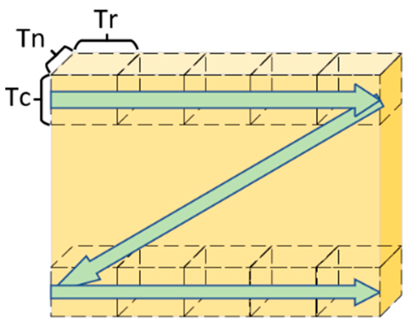
Due to the limited on-chip storage resources of FPGA, it is impractical to cache the entire feature map and all weights. Therefore, on the basis of existing research, this paper adopts a refined resource management strategy that divides the input feature map and weight data into several smaller blocks. Each time, a small block of data is read from the DDR memory for convolution calculations, and the results are stored back in DDR, gradually completing the entire convolution operation. Specifically, the input feature map, weights, and output feature map are all partitioned into several small blocks. Only the small block of data required for the current computation is loaded into the on-chip memory, and after completing the computation, the results are written back to external memory before loading the next batch of data blocks. As shown in
Figure 2, the parameters Tr, Tc, and Tn represent the sizes of the data blocks along the row, column, and channel dimensions, respectively. This block-moving strategy enables the algorithm to dynamically handle feature maps of different sizes, processing only one small block at a time, thereby effectively utilizing on-chip storage space [
19]. Additionally, this block strategy can adapt well to varying hardware configurations. By adjusting the block sizes (e.g., Tc and Tr), system performance can be optimized, achieving the best computational efficiency and balance under the given on-chip storage resource constraints.
In addition to data partitioning, data reuse is also a key strategy in the refined resource management approach for FPGA accelerators to reduce power consumption and improve computational efficiency. Data movement is a major source of power consumption; therefore, minimizing the number of data transfers and enhancing data utilization efficiency is of great significance. In convolution computation, some intermediate computation results can be temporarily stored in registers for subsequent computation to avoid frequent writing back to DDR and re-reading. In the absence of dependencies between data, the computing unit can perform all related operations on-chip as much as possible, reducing the number of intermediate results moved. At the same time, by caching the input feature map in on-chip memory or registers, multiple convolution kernels can process the same feature map in parallel. In this way, the feature map only needs to be read from DDR once and can be reused on multiple computing units, reducing the overhead of repeatedly loading the input feature map. This reuse method significantly improves data usage efficiency by sharing the same feature map data across multiple computing units and reduces the number of accesses to external memory.
FPGAs have strong parallel processing capabilities, and convolutional neural networks (CNNs) contain many output channels. Channel unfolding allows FPGA to compute units to process multiple channel computation tasks simultaneously, significantly increasing throughput and accelerating the entire convolution process [
20]. As shown in
Figure 3, the terms Tn and Tm represent the sizes of the input and output channels of the block data, during the implementation of channel unfolding, the computations for each output channel share the same input data, resulting in a high data reuse rate. Since different output channels perform calculations at the same input locations, this reduces the need for frequent data access to external memory. This not only alleviates the pressure on memory bandwidth, but also decreases data transfer latency, thereby improving the overall energy efficiency of the system.
The refined resource management strategy integrates three methods: data partitioning, data reuse, and channel unfolding. This approach not only addresses the issue of limited on-chip storage resources, but also reduces power consumption by minimizing data movement. Additionally, it enables dynamic handling of feature maps of varying sizes. Through reasonable segmentation and dynamic management of computation tasks, this strategy not only alleviates the constraints of storage resources, but also enhances data processing efficiency, significantly improving the overall performance and energy efficiency of FPGA accelerators.
3.1.2. Dynamic Switching Double Buffering Strategy
To enhance the parallelism of computation and data access, based on existing research, this paper proposes an architectural optimization strategy that utilizes dynamic switching of double buffering to achieve parallel computation and data transfer. This scheme alternates between two sets of buffers for data loading, computation, and storage operations, thereby overlapping convolution computation with access to external memory (DDR), which improves the overall system efficiency.
As shown in
Figure 4, the core of the dual ping-pong operation lies in dividing the computation unit and storage unit into two independent modules [
21]. Each module is equipped with two sets of buffers used for the current block’s computation and the storage of the previous computation results. In each convolution computation cycle, the system determines which buffer to use for computation based on a ping-pong flag. For example, when ping-pong is true, the system performs convolution computation in buffer fm_out2 while simultaneously storing the output data in buffer fm_out1 to DDR. Conversely, when ping-pong is false, the system performs computation in fm_out1 and writes the data in fm_out2 to DDR. This alternating operation allows the computation unit and storage unit to operate concurrently, eliminating waiting during data loading or storage. From a local perspective, the convolution computation unit also employs similar parallelized processing. In each convolution cycle, the loading of convolution kernel weights and feature map data occurs simultaneously with the computation. By pre-loading the data required for the next computation block during the computation process, the system further reduces the data loading overhead, achieving complete overlap between computation and data transfer.
The advantages of this scheme lie in its full utilization of hardware resources and minimization of data access waiting time. Compared to the traditional single-buffer scheme, the dual ping-pong operation scheme enables seamless switching between data loading, computation, and result storage through highly parallel computation and storage operations. This mechanism effectively increases convolution computation throughput, particularly when processing large-scale feature maps, significantly reducing the performance bottleneck caused by DDR access.
3.1.3. Winograd Convolution Algorithm
The Winograd convolution algorithm is a fast convolution algorithm that improves efficiency by reducing the number of multiplication operations. It employs a clever transformation method that converts convolution operations into matrix multiplications and reduces the required multiplication operations through pre-computed transformation matrices.
With one-dimensional input data
and one-dimensional convolution kernel
, using ordinary matrix multiplication, a total of six multiplications and four additions are required.
Winograd’s
F (2, 3) fast calculation method (2 refers to the number of elements output, 3 refers to the filter size) is as follows:
In the inference stage, on the basis of existing research, the elements on the convolution kernel are fixed, so the equations related to g in the above equation can be calculated in advance and are only calculated once in the prediction stage and can be ignored. So, a total of four multiplications plus four additions is required here. In essence, Winograd’s algorithm, by operating in the transform space, converts the multiplication operation that needs to be repeated several times in the original space into a multiplication operation that only needs to be performed once in the transformed space. The addition implementation inside the FPGA requires much less resources than the multiplication implementation and is also more resource efficient.
The 2D Winograd convolution algorithm is a further extension of the 1D Winograd algorithm. For example,
F (2 × 2, 3 × 3) refers to performing convolution on a 4 × 4 matrix using a 3 × 3 convolution kernel and then calculating according to the one-dimensional approach.
Specifically, the Winograd algorithm transforms the input feature map and convolution kernel into smaller matrix forms. This transformation process utilizes special transformation matrices designed such that the resulting matrix product is equivalent to the original convolution operation. After the transformation is complete, the algorithm performs element-wise multiplication, which requires fewer multiplication operations than directly performing the convolution. Finally, the algorithm transforms the product results back into the final output feature map using another transformation matrix. It is important to note that while the Winograd algorithm reduces the number of multiplications, it increases the number of additions. However, in modern computer architectures, the cost of multiplication operations is typically much higher than that of additional operations, thus allowing the Winograd algorithm to still provide significant performance improvements. The Winograd algorithm is particularly well-suited for small convolution kernels (3 × 3), as these small convolution kernels are very common in deep learning.
3.1.4. Pooling Computation Optimization Strategy
In deep learning, pooling is an important downsampling technique that is widely used in CNN. Pooling layers can significantly reduce the size of feature maps, thereby decreasing the number of parameters in the model, reducing computational complexity, and preventing overfitting. This also enhances the model’s generalization ability. Different pooling methods can extract different types of features: max pooling tends to capture the most prominent features in an image, while average pooling focuses on extracting the average features of an image. Feature extraction helps the model better learn the critical information in an image, improving the accuracy of classification or recognition tasks.
represents the max pooling output value in the rectangular region
with respect to the K feature map, and
represents the element located at
in the rectangular region
. In FPGA accelerators, pooling is a commonly used operation that helps reduce computational load, lower the risk of overfitting, and improve the generalization ability of the model. The input feature map is loaded into the buffer by channel, height, and width blocks, and then traversed with a 2 × 2 window [
22].
The maximum value is calculated within each window and the result is stored in the corresponding position of the output feature map. The entire process improves the speed and efficiency of the pooling operation through block loading, computation, and storage. Given the relatively low computational load of the pooling module in the overall resource allocation, only parallel expansion is implemented here.
The data input module is designed with four row buffers, which read data in parallel from four different DDR ports into the row buffers and compute the maximum value within the pooling window. After this comparison, the obtained maximum value is written into the output buffer. By using pipeline instructions, the rows and columns of the feature map are loop unrolled into a pipeline to achieve the goal of processing one data element per clock cycle, thereby reducing the overall processing time. The speed of the pooling operation is enhanced by parallel processing of multiple pooling units. The outer loop in the code uses two nested loops to traverse the rows and columns of the feature map, while the inner loop for the channels is unrolled using the UNROLL directive. This means that the operations within the loop are executed simultaneously, achieving parallel processing. The pooling tree is illustrated as shown in
Figure 5.
3.2. Timing Optimization
To analyze the system bottleneck, we utilized the analysis report generated by the HLS tool, which provides a comprehensive analysis of design performance, including resource utilization, timing paths, and critical path analysis. We focused on the worst negative slack (WNS) and critical path analysis in the report. The WNS metric indicates whether the design meets timing constraints, while the critical path analysis reveals the primary factors limiting the system frequency. The analysis results show that the critical path is located in the convolution computation unit of the image processing module. Further analysis revealed that the delay in the multiplier chain of this unit was excessively high, leading to timing violations. The multiplication operations were converted into shift and add operations. In HLS, this optimization can effectively improve timing performance by leveraging hardware characteristics. In hardware, multipliers are much more complex than adders and shifters, requiring more resources and time to complete operations. Shifters and adders are the most basic computational units in hardware and are executed very quickly.
As shown in
Figure 6, it is difficult to complete the judgment of four conditions in serial within one operation clock cycle, which will cause WNS. Therefore, the area of the chip can be sacrificed for performance improvement, and it is divided into four small parts for parallel judgment operation. In order to improve the working frequency of the hardware circuit, this study optimizes the complex conditional statements in the code. To enhance the operating frequency of the hardware circuit, this study optimized the complex conditional statements in the code. The original multiple conditional checks involved multiplication, addition, and comparison operations, resulting in a complex logical structure. These operations were difficult to complete within a single clock cycle, leading to a long critical path that limited the maximum operating frequency of the circuit. By breaking down the complex conditional statements into independent Boolean expressions and precomputing partial results in parallel, the critical path was effectively shortened. Ultimately, a frequency of 200 MHz was achieved under limited resource conditions.
3.3. Interface Optimization
In the design flow of HLS, the #pragma HLS INTERFACE directive plays a critical role in the innovative introduction of delay optimization instructions, as it is used to specify the attributes of the external hardware interface. This becomes particularly important when performing large-scale read and write operations to DDR memory, where interface optimization is crucial. Given the inherent latency characteristics of DDR access, if each operation in the HLS design must wait for DDR access to complete, performance bottlenecks are inevitable. To alleviate this issue, this paper proposes a method that sets an expected AXI4 interface latency, allowing the design to initiate bus requests several clock cycles ahead of the actual read or write operation. This strategy enables the execution of other tasks during the DDR response wait time, effectively hiding DDR access latency, and helps build a more efficient pipeline, thereby improving the overall system throughput.
Furthermore, by binding ports and buses at the interface level, mapping interface signals (such as address, data, and control signals) to specific AXI buses can significantly enhance the clarity and manageability of system-level interconnections. The implementation of independent AXI interfaces allows for the full utilization of the data bus’s advantages, enabling parallel data reads. Additionally, by binding multiple logical ports to the same physical AXI interface, the number of interfaces is reduced, saving hardware resources. This is important in managing the interconnections between multiple AXI masters and slaves in complex systems.
For port read operations, using burst transfer mode and setting a larger burst length for readings can significantly improve reading efficiency. Compared to random access, accessing data from consecutive addresses is far more efficient. By maximizing the burst length, the number of DDR accesses is reduced, which lowers the average access latency, thereby increasing data transfer speed.
In summary, the optimization measures described in this paper can significantly improve system performance during frequent DDR access by reducing latency, increasing throughput, and more effectively utilizing available bandwidth. These improvements are particularly valuable for data-intensive applications, offering substantial practical benefits.
3.4. Precise Bit Width Tuning Quantization Strategy
In FPGA design, based on existing research, fixed-point quantization is the process of converting floating-point numbers into fixed-point representations [
23]. This approach reduces the data bit width, thereby minimizing the required storage space and computational resources, which is particularly important for resource-constrained embedded devices. During deep learning inference, using fixed-point numbers can significantly improve FPGA processing speed and efficiency while maintaining sufficient numerical precision [
24]. Linear quantization is the most commonly used quantization method. It first determines the range of the floating-point data and selects an appropriate scaling factor to ensure all floating-point numbers are mapped within the representable range of fixed-point numbers. The quantized fixed-point values are then stored in DDR for computation. The formula for quantization is as follows:
where Q represents the quantized fixed-point number, round is the rounding function,
x is the original floating-point number,
Z is the zero-point used for asymmetric quantization (
Z = 0 for symmetric quantization), and
s is the scaling factor.
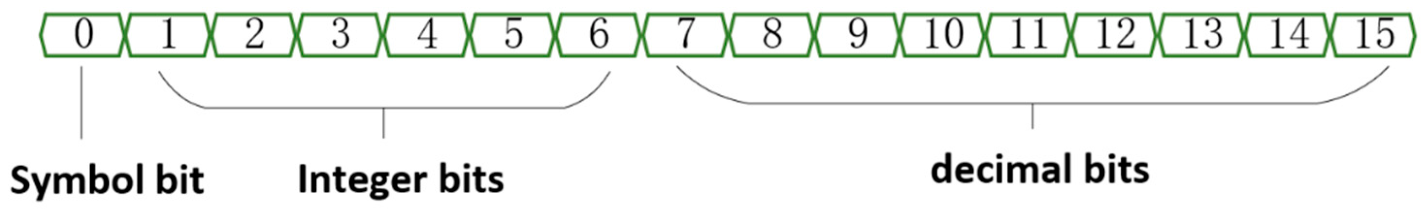
In fixed-point representation, the total bit width (16 bits is chosen in this paper) is fixed, as shown in
Figure 7, with the first bit representing the sign bit and the remaining 15 bits representing the value of the data. The allocation of integer and fractional bits directly impacts the range and precision of the numerical values. By adjusting the ratio of integer to fractional bits, an optimal balance can be achieved between numerical range and representation accuracy. The optimal bit width allocation may vary for different network layers or models. While increasing the number of fractional bits can enhance the precision of numerical representation, a reduction in integer bits limits the range of representable values.
3.5. BN Layer Fusion
Batch Normalization (BN) is a technique used to accelerate the training of deep neural networks. It enhances training speed and model performance by standardizing the input of each layer, giving it a more stable distribution.
BN fusion is a common technique for optimizing and deploying deep learning models, which is especially significant in hardware acceleration. BN fusion refers to the process of merging BN operations with the adjacent linear layers into a single operation during the model deployment phase, thereby eliminating runtime BN operations. This reduces computational complexity. Through BN fusion, the BN computation is completely integrated into the convolutional layer, requiring only a single matrix multiplication and addition, which significantly reduces computational complexity. It also lowers memory requirements. In the inference stage, the original BN operation requires loading additional parameters and performing calculations on them. By fusing, the BN parameters can be directly incorporated into the weights and biases, reducing memory access and parameter storage. This is especially important for devices with limited bandwidth, such as FPGA.
In an FPGA accelerator, BN fusion refers to the process of merging the batch normalization operation with convolution or other layer operations. This fusion reduces the complexity of the model, improves computational efficiency, decreases the number of computation steps, and reduces memory access, thereby enhancing the overall performance of the system [
25]. By combining the convolutional layer’s weights with the scaling and shift parameters from the BN layer, new weights and biases are generated. In FPGA design, this approach allows for better utilization of the FPGA’s customization advantages, increasing the inference speed of deep learning models, particularly in resource-constrained embedded systems.
During the training phase, the mean, variance, and scaling and shift parameters of the BN layer are computed. These parameters are fixed once training is complete. For each convolutional layer weight W and corresponding BN layer parameters, the new weight
W′ can be calculated using the following formula:
The new offset
can be calculated using the following formula:
Here, represents the bias of the original convolutional layer, while μ and σ2 are the mean and variance of the BN layer, respectively. γ and β are the scaling and shifting parameters of the BN layer, and ε is a small constant used to prevent division by zero.
4. Discussion
4.1. Experimental Platform
The accelerator designed in this paper utilizes the ZYNQ series as the development platform, with the main chip being the XC7Z020CLG400-2 device. This device features 220 DSP48E processing units, 53,200 lookup table (LUT) logic resources, and 140 BRAM36K memory resources. Additionally, the accelerator is equipped with extended peripherals and cache memory; the onboard DDR3 chip can effectively handle applications requiring large memory and high bandwidth. The processing system (PS) employs a dual-core Cortex-A9 architecture and is synthesized using the Vivado 2019.2 tool, achieving an operating frequency of 200 MHz for the accelerator system.
4.2. Accuracy Evaluation
In the experiments, this study utilized a convolutional neural network model based on YOLOv4-Tiny and converted all floating-point operations to their corresponding fixed-point operations. To investigate the impact of different quantization strategies on image recognition accuracy, two fixed-point data types, data_t, with varying bit widths and representation formats, were defined [
26]. As shown in
Figure 8, the following two quantization strategies were employed:
ap_fixed <W, I, Q, O> is a fixed-point data type in Xilinx’s Vitis HLS (High-Level Synthesis). W: total bit width; I: number of integer bits; Q: quantization mode; and O: overflow mode. The bit width of a fixed-point number consists of the sign bit + integer part + fractional part:
Sign bit: the most significant bit (MSB) is the sign bit, used to indicate whether the value is positive or negative.
Integer part: occupies (I-1) bits (including the sign bit).
Fractional part: the remaining bits represent the fractional part, i.e., (W-I) bits.
Examples: ap_fixed <16,6, AP_RND_CONV,AP_SAT>: This represents a 16-bit-wide fixed-point number, with 5 bits allocated for the integer part and 10 bits for the fractional part. This strategy uses a rounding mode to the nearest number (AP_RND_CONV) and performs saturation processing (AP_SAT) in case of overflow during computations. ap_fixed <16,6> range: [−32, 31.9990234375] precision: 0.0009765625
ap_fixed <16,7, AP_RND_CONV,AP_SAT>: This represents a 16-bit-wide fixed-point number, with 6 bits allocated for the integer part and 8 bits for the fractional part. Its other characteristics are the same as the first quantization strategy. ap_fixed <16,7 > range: [−64, 63.998046875] precision: 0.001953125
For weight data that require a precision of 0.001, ap_fixed <16,6> is more suitable to meet the requirements.
By comparing the recognition accuracy under two quantization strategies, it was observed that the quantization strategy using 6-bit integers achieved an accuracy of 90.3%, which is superior to the 61.7% accuracy of the 7-bit integer strategy. This indicates that with an increase in fractional bit width, the model can maintain higher accuracy. The reason for this is that a greater bit width allows for a more precise numerical representation, thereby reducing quantization errors. This experiment demonstrates that the quantization strategy has a direct impact on the accuracy of image recognition models. By appropriately increasing the fractional bit width, it is possible to reduce the accuracy loss caused by quantization while maintaining low hardware resource consumption.
4.3. Experiment Performance Evaluation Experiments
4.3.1. Iteration Interval Optimization Experiments
The Iteration Interval (II) refers to the time interval between the initiation of two consecutive operations, which is particularly critical for achieving high-performance hardware accelerator designs. The timing interval of task initiation has a direct impact on the performance and throughput of the design. If the initiation interval between tasks is too short, the FPGA may be unable to process the tasks promptly, leading to conflicts. Conversely, if the initiation interval is excessively long, it may result in wasted FPGA resources, thereby diminishing overall performance. Given the heavy reliance on for-loops in convolution operations, special attention must be paid to the II. The time interval of each iteration directly influences the overall performance of the loop. By optimizing the II, it is possible to achieve pipelining of the loop, which enhances throughput and efficiency.
As shown in
Figure 9, assuming the loop has three typical operations, read, compute, and write, represented by RD, CMP, and WT, respectively, each operation can be completed within a single clock cycle. The II is 3, meaning that each iteration requires the read, compute, and write operations to be completed. In the case of executing n iterations, completing the loop requires 3n clock cycles. By employing pipelining, it is possible to enhance processing capabilities without significantly increasing core logic resources. Each iteration’s read, compute, and write operations are executed in a pipelined manner, resulting in an II of 1. Thus, when executing n iterations, completing the loop requires n + 2 clock cycles. As n increases, the speedup approaches a factor of 3.
Conduct experiments to optimize the II for the convolution module, pooling module, and upsampling module. Considering the data dependencies between computations, efficient execution with an II of 1 can be achieved by changing the order of the loops.
Convolution module: as shown in
Table 1, the input feature map of 4 × 27 × 27, convolution kernel of 32 × 4 × 3 × 3, and output feature map of 32 × 13 × 13, the unoptimized implementation would require 3 × 3 × 13 × 13 × 32 × 4 = 584,064 clock cycles. Considering the resource constraints of edge devices, we implement complete unrolling on both input and output channels, enabling 32 × 4 = 128 multiplication operations simultaneously, which reduces the clock cycles by a factor of 128. By incorporating pipeline operations, we achieve an additional approximately 3-fold reduction. Consequently, serial loop execution is required across the convolution kernel dimensions and output feature map spatial dimensions for 3 × 3 × 13 × 13 = 1521 iterations to complete all convolution computations. As shown in
Table 2, the trip count of 1521 aligns with theoretical calculations. In practice, additional operations such as auto-increment require 20 extra clock cycles, resulting in a total of 1539 clock cycles for completing the convolution computation. This represents approximately a 384-fold reduction compared to the initial clock cycle requirement.
Pooling module: The cached data read in each operation are sized at 4 × 26 × 26, requiring only simple comparison operations rather than complex calculations. The design is enhanced from a single input and output channel to four parallel input/output channels by partitioning the input and output feature map buffer into four segments to support parallel processing. As shown in
Figure 10, parallel data reading is implemented at the feature map channel level, with four read address requests occurring simultaneously within the same clock cycle. Serial execution at the feature map’s spatial dimensions (rows and columns) requires 26 × 26 = 676 clock cycles. Through full pipeline implementation for parallel execution, and accounting for additional data computations in practical implementation, the total execution requires 732 clock cycles.
Upsampling module: The input data array containing original low-resolution data, with an input feature map size of 128 × 13 × 13 and an output feature map size of 128 × 26 × 26, where each input data point is replicated to four different positions to generate a larger output image. Theoretically, for each input data point, four output data points are required, resulting in 128 × 13 × 13 = 21,632 clock cycles. In practical implementation, considering the latency of address access operations, the total execution requires 21,706 clock cycles.
4.3.2. Timing Optimization Experiments
In HLS, multiplication operations typically consume more resources and time compared to shift and addition operations, especially on resource-constrained hardware platforms such as FPGAs. Replacing multiplication with shift and addition operations can significantly enhance design efficiency as shown in
Table 3. This is because shift operations are straightforward for implementing in hardware, requiring only the reconnection of wires, and addition operations are generally faster and more resource-efficient than multiplication. For instance, multiplying by specific constants can often be replaced by a series of shifts and additions. This optimization technique is particularly beneficial in embedded systems and performance-critical applications, as it reduces the computational burden on the processor, lowers power consumption, and improves overall performance. Consequently, it effectively optimizes code, reducing resource consumption and enhancing performance.
In HLS, overly lengthy conditional statements can lead to overly complex circuit logic in the generated design, resulting in the inability to complete all conditions within a single clock cycle. This situation can introduce negative slack, thereby increasing latency and reducing the operating frequency of the circuit. By breaking down complex conditional statements into multiple smaller, simpler conditions, it is possible to effectively simplify the logic and reduce latency. This approach allows synthesis tools to optimize more easily, ultimately improving the overall performance of the circuit and achieving an operating frequency of up to 200 MHz.
4.3.3. Ablation Experiments with Multiple Strategies
The previous discussion analyzed the optimization strategies for FPGA accelerators across various modules. As shown in
Table 4, the work outlined was systematically deployed and experimented with to observe the impact of different modules on the overall performance of the neural network. With BN fusion, fine-grained bit width tuning quantization, and Wino convolution, the measured execution time was 547 ms. In contrast, using BN fusion, fine-grained bit width tuning quantization, and standard convolution resulted in a measured execution time of 384 ms. This difference arises because the Wino algorithm requires additional preprocessing and postprocessing steps before and after performing convolution operations. These steps include matrix transformations of the input feature maps and convolution kernels, as well as converting the output results back to standard formats. Such additional computations increase the overall execution time, and the Wino algorithm necessitates more memory access to store intermediate transformed data. On resource-constrained FPGAs, the limited memory bandwidth means that frequent memory accesses can lead to performance bottlenecks, causing the overall execution time for the Wino algorithm to exceed that of standard convolution.
By adopting a refined resource management strategy, the necessary computation data can be cached on chip. This allows multiple sets of cached data to perform up to hundreds of multiply accumulate operations each clock cycle. After optimizing the point-wise convolution (pwconv), pooling, and upsampling operations as listed in
Table 1, the execution time was reduced to 311 ms. Additionally, optimizing the FPGA operating frequency to 200 MHz significantly decreased the critical path processing time, resulting in a processing time of 199 ms, marking this as the most effective optimization strategy. Further improvements were achieved by optimizing the FPGA interface, which reduced the processing time to 185 ms, indicating that interface optimization plays a crucial role in enhancing data transfer efficiency. Ultimately, the overall performance improvement amounted to 52.2%.
4.4. Resource Utilization
Table 5 lists the different submodules of the accelerator and the percentage of system resources they consume on the hardware platform. There are four submodules: stdconv, pwconv, maxpool, and usample.
LUT: This is the basic unit used to implement combinational logic in FPGAs. The values in the table represent the percentage of lookup table resources used by each accelerator. The stdconv accelerator occupies 94% of the LUT resources.
BRAM_18K: This refers to the block RAM resources in the FPGA, typically used for data storage. The values in the table indicate the percentage of BRAM_18K resources utilized by each accelerator. For instance, the pwconv accelerator uses 11% of the BRAM_18K resources.
DSP48E: This resource is used for performing multiplication, addition, and other mathematical operations. The values in the table reflect the percentage of DSP48E resources consumed by each accelerator. The stdconv accelerator utilizes 70% of the DSP48E resources.
FF: The values in the table show the percentage of flip-flop resources used by each accelerator. The maxpool accelerator occupies 3% of the FF resources.
Through the synthesis with HLS tools, some resources exceed 100%. These utilization figures are estimations, and further optimizations will be applied during RTL synthesis in Vivado, which will reduce the resource utilization.
Table 6 illustrates the FPGA resource utilization in this study. The entire accelerator consumed 39,328 LUT, accounting for 73.92% of the total; 48,077 FF flip-flops, representing 45.19% of the total; 215 DSP, utilizing 97.73% of the available units; and 96 BRAM, occupying 68.57% of the total. The high utilization rates of LUT and BRAM indicate excellent resource optimization, efficiently leveraging the FPGA’s internal resources to achieve the required functionality. DSPs are the primary computational resources for addition and multiplication operations, with a utilization rate reaching 97%.
A high DSP utilization rate is a key feature of this design. To maximize computational performance within the constraints of a small FPGA, the DSPs are primarily employed for the multiplication operations in convolutions. This high utilization rate aims to enhance the parallel processing capability of convolution to the greatest extent possible.
In terms of scalability, the ZYNQ7020 is composed of a PL section and a PS section. The PL section implements fundamental deep learning operators such as convolution, pooling, and upsampling. The PS section provides functionality for deep learning computation control, task scheduling, and model management. The PS section can load and manage different deep learning models via software, supporting the execution of everything from simple shallow neural networks to complex deep convolutional neural networks. By leveraging the hardware acceleration capabilities of the PL section, the system can dynamically deploy and switch between models, meeting the inference requirements of various scenarios. Through the efficient collaboration of the PS and PL, high-performance, low-power deep learning inference acceleration is achieved.
For portability to different FPGA systems, the high utilization only uses 215 DSPs. For boards with fewer resources, the FPGA cannot achieve an acceleration effect. On boards with more resources, minor code modifications can further improve inference speed. This demonstrates that this study fully exploited the FPGA’s computational resources and maximized computational parallelism to the extent possible.
4.5. Comparison of Other Deployed Neural Network Platforms
The research achievements in implementing YOLO series algorithms on FPGA platforms are substantial. This paper conducts a comparative analysis of the research results with relevant literature. By delving into the data presented in
Table 7, we can observe trends in several key performance indicators. In terms of latency performance, the proposed platform demonstrates outstanding results, with a latency of only 185 ms, which is lower than that of the other three platforms. This is particularly crucial for applications requiring rapid response. Regarding DSP utilization, the platform achieves superior computational performance with a relatively lower number of resources. In terms of operations per second (GOPS), this paper leads with a score of 36.97 GOPS, compared to 9.24 GOPS in Paper 1 and 18.32 GOPS in Paper 3, showcasing the excellent performance of this platform in handling extensive computational tasks. In terms of power consumption, the processor presented in this paper has the highest energy usage, reaching 4.19 W. This is due to the processor’s ability to enhance processing speed and computational efficiency, which consequently increases energy consumption. However, in terms of energy efficiency ratio, this paper leads with a value of 8.82 GOPS/W, outperforming the 3.23 GOPS/W reported in Paper 1. This result highlights the advantages of the proposed platform regarding energy efficiency, effectively reducing power consumption while maintaining high performance.
In summary, the platform proposed in this paper demonstrates outstanding performance across multiple metrics, especially in reducing latency, enhancing computational capability, and improving energy efficiency. These results provide valuable insights for future research, particularly in applications that demand both high responsiveness and processing power.
4.6. Limitations
Although the optimization acceleration strategy and method proposed in this study achieved remarkable results in the fast inference of the YOLOv4-Tiny model on the FPGA platform, there are still some limitations that deserve further discussion and improvement:
Platform dependence and generality: The experimental verification of this study mainly focuses on the ZYNQ7020 FPGA platform. Although the results show the effectiveness of the strategy, the performance of the strategy on other FPGA platforms, such as FPGA with different architectures and different resource scales, has not been fully verified. The differences in the hardware characteristics of different platforms may affect the efficiency and optimal parameter configuration of resource management policies. Therefore, the cross-platform versatility of policies needs to be further studied and verified.
Network architecture adaptability: This optimization strategy is mainly designed and optimized for the specific object detection network YOLOv4-Tiny. Although the strategy contains general techniques such as dynamic resource management and bit width adjustment, its optimization effect and applicability still need to be evaluated when applied to other types of object detection networks, such as deeper and more complex network structures (e.g., YOLOv5, YOLOv7, or Transformer). The computational patterns, data dependencies, and parameter distributions of different network architectures may require targeted optimization strategy adjustments.
Quantization accuracy tradeoff: Quantization operation with dynamic bit width adjustment aims to improve energy efficiency and computational performance. Although the experimental results show that the accuracy loss is controllable on the metal surface defect dataset, in other application scenarios with higher accuracy requirements, it is necessary to more carefully weigh the relationship between performance improvement and accuracy loss brought by quantization and explore more advanced quantization techniques to maximize the performance gain under the premise of ensuring accuracy.
Consideration of practical application scenarios: This study focuses on the optimization of the algorithm level and the acceleration implementation on the FPGA platform. However, in real-world deployment, more engineering considerations need to be considered, such as power management, thermal design, system integration, and interface design with external sensors or actuators. The consideration of these practical application scenarios may pose new constraints and challenges for the design of accelerators, which need further attention in future research.
5. Conclusions
In this paper, we introduced a parallel FPGA acceleration architecture for CNN specifically designed for embedded applications to overcome the limitations of latency and energy consumption inherent in traditional platforms. Our experimental results demonstrate the effectiveness of this architecture, achieving a significant reduction in single-image processing latency to 185 ms and delivering a high performance of 36.97 GOPS. These metrics underscore the superior speed, power efficiency, and resource utilization offered by our FPGA-based solution, highlighting the inherent advantages of FPGA for parallel computing in low-power, high-speed CNN applications. This work is particularly timely and relevant given the increasing demand for deploying CNNs on embedded and mobile devices.
This research establishes a robust foundation for the development of efficient FPGA-based CNN accelerators, paving the way for the broader adoption of high-performance, low-power deep learning in resource-constrained embedded systems. To further advance this field, future research should prioritize the following key directions:
Scalability and adaptability to advanced models: investigating the architecture’s scalability and adaptability to accommodate more complex and deeper CNN models, including emerging Transformer-based vision models.
Integration of advanced optimization techniques: Exploring the synergistic integration of optimization techniques such as quantization and pruning with our parallel architecture to further minimize resource consumption and enhance energy efficiency. Furthermore, research into FPGA-tailored dataflow optimization techniques could unlock even greater throughput and latency reductions.
In-depth energy efficiency analysis and hardware-level optimization: conducting comprehensive energy profiling and optimization at the hardware level and exploring techniques such as clock gating, power gating, and voltage scaling to achieve further energy consumption minimization.
By actively pursuing these future research directions, we are confident that FPGA-based CNN accelerators can achieve even greater levels of performance and efficiency, solidifying their critical role in enabling high-performance embedded deep learning.


