Article

High-Precision Time Synchronization Based on Timestamp Mapping in Datacenter Networks

1
National Network New Media Engineering Research Center, Institute of Acoustics, Chinese Academy of Sciences, No. 21, North Fourth Ring Road, Haidian District, Beijing 100190, China
2
School of Electronic, Electrical and Communication Engineering, University of Chinese Academy of Sciences, No. 19(A), Yuquan Road, Shijingshan District, Beijing 100049, China
*
Author to whom correspondence should be addressed.
Electronics 2025, 14(3), 610; https://doi.org/10.3390/electronics14030610
Submission received: 18 December 2024 / Revised: 24 January 2025 / Accepted: 1 February 2025 / Published: 4 February 2025
(This article belongs to the Topic Advanced Integrated Circuit Design and Application)

Abstract

:
In datacenter networks, it is necessary to determine whether the path is congested according to the one-way delay of packets. The accurate measurement of one-way delay depends on the high-precision time synchronization of the source device and destination device. We have proposed a time synchronization method based on timestamp mapping, combined with in-band network telemetry technology to obtain the packet send timestamp and receive timestamp on devices. The results show that the maximum synchronization error is 19 ns, and the standard deviation is 7.8 ns with a 100 ms time synchronization period and offset adjustment strategy. The proposed time synchronization method achieves outstanding synchronization accuracy and stability.

1. Introduction

In some critical application scenarios, it is essential for systems to coordinate consistently in time to ensure data consistency, integrity, and timeliness. This is particularly important in distributed systems and high-performance computing networks, where time synchronization not only influences data processes and storage but also significantly impacts network performance, reliability, and security. As the speed of datacenter network links continue to improve, various distributed applications and network scheduling demand higher-precision time synchronization [1]. High-precision time synchronization enables researchers to obtain an accurate one-way delay for network monitoring and administration. Additionally, fine-grained packet-level scheduling in a datacenter can relieve congestion and enhance network performance, which requires effective time synchronization among network devices [2].
In modern datacenters, network performance and flexibility are critical for satisfying large-scale computing, storage, and communication demands. The rapid advancement of technologies such as cloud computing, artificial intelligence, machine learning, and virtualization have led to increasingly complex network requirements in datacenters. There are a large number of network communication demands in datacenters, especially in the case of high concurrency, low latency, and high throughput. Standard protocols may bring large protocol overhead and performance bottlenecks. Custom protocols can be optimized for the specific needs of the datacenter; they also can be adjusted flexibly according to different service scenarios and technology trends to better support the changing requirements of datacenters. To facilitate the application of custom protocols, P4-based programmable switching [3] and Smart Network Interface Cards (SmartNICs) [4] are widely deployed in datacenters. Traditional switches manage network traffic through fixed functionalities; in contrast, programmable switches enable the customization and updating of network process logic to accommodate evolving requirements [3,5]. Datacenter networks typically involve extensive high-speed packet process tasks, including packet routing, filtering, load balancing, traffic monitoring, and various other operations [6]. Field-Programmable Gate Arrays (FPGAs) have gained widespread adoption in datacenter network acceleration (such as FPGA-based SmartNIC) due to their high-performance parallel computing capabilities and inherent flexibility, particularly in using custom network protocols scenarios [7].
Network devices depend on path state changes between the local and the next-hop devices to adjust the local traffic sending rate. Congestion control implemented on the FPGA requires the measurement of the one-way delay of packets between the local device and the next-hop device to determine whether the path experiences congestion [8]. Devices maintain a timestamp to record the occurrence of events. The calculation of the one-way delay is based on the packet’s send time on the source device and the receive time on the destination device [9,10]. If the timestamps of the source device and destination device are not synchronized, it is impossible to accurately calculate the one-way delay. Consequently, it is essential to synchronize the timestamps of devices before measurement.
There are several technical challenges associated with implementing time synchronization between the FPGA and the programmable switch. Firstly, due to hardware design and external environmental factors, the actual operating frequency of the FPGA may not match the configured frequency, therefore it is hard to determine exactly how long a clock cycle is. Secondly, modification to the existing data-plane clock of the switch is forbidden for the following reasons: (1) rewriting the internal data-plane clock is an expensive operation since it involves consistency checks and (2) other applications such as in-band network telemetry (INT) may be using the data-plane clock in parallel [11]. These limitations increase the complexity and challenge of time synchronization.
INT has received a lot of attention from industry and academia in recent years. Unlike traditional network measurement techniques, INT combines packet forwarding with network measurement; the internal state of the network is collected and inserted into telemetry packets by the forwards’ nodes (such as programmable switches and SmartNICs), so the INT has the advantages of real-time, fine measurement granularity and rich measurement states.
In this paper, we address the time synchronization challenge associated with an FPGA-based SmartNIC and programmable switch. We propose a time synchronization method based on timestamp mapping, which combines INT technology to obtain the packet send and receive timestamps of the FPGA and switch. The contributions of this paper are outlined as follows:
  • We present an innovative time synchronization method based on timestamp mapping, elaborate the principle and steps of the method, and make a detailed description of the implementation on an FPGA and programmable switch;
  • We introduce the evaluation method and build a test platform to evaluate the feasibility and effectiveness of the method. Firstly, we investigate the effect of the synchronization period on the time synchronization performance, and secondly, we optimize the synchronization method using an offset adjustment strategy. Using the 100 ms time synchronization period and the offset adjustment strategy, the maximum synchronization error of the proposed method is found to be 19 ns, and the standard deviation is 7.8 ns. These results indicate a high level of synchronization accuracy and stability.

2. Related Work

Global Positioning System (GPS) time synchronization [12,13] is a technology that synchronizes ground equipment clocks using a high-precision time source provided by a satellite’s internal atomic clock. It is widely used in various fields that require accurate time synchronization. With the wireless signal transmitted by GPS, ground receiving devices can recover time and frequency information from the signal, achieving a synchronization accuracy of less than 20 ns. This method exhibits robust resistance to interference and maintains exceptionally high accuracy. However, the system necessitates the installation of dedicated GPS timing units in each terrestrial device, which can be prohibitively expensive for widespread deployment. Additionally, the system typically requires signals from at least four satellites at the same time to achieve synchronization, limiting its effectiveness in shielded environments.
The Network Time Protocol (NTP) [14] and Precision Time Protocol (PTP) [15,16] are widely used time synchronization protocols, which transmit time information from a master clock through Ethernet packets. The synchronization principle of the NTP and PTP involves recording timestamps between the master clock and the slave clock, exchanging timestamps, and calculating the time offset between the slave clock and the master clock using four timestamps, thereby correcting the slave clock to achieve time synchronization between the two devices. However, the NTP completely relies on a software timestamp; network fluctuations and delay during transmission greatly affect the synchronization accuracy, resulting in a synchronization accuracy of only milliseconds. In contrast, the PTP uses special hardware to assist the realization of physical-layer timestamp marking, avoiding the uncertainty of network time; its synchronization accuracy can reach the sub-microsecond or even nanosecond level.
Synchronous Ethernet (SyncE) [17,18] is a time synchronization technology based on a link-layer data stream, which realizes time synchronization among nodes by embedding timestamp information into the data stream. This technology enables the recovery of the transmitter’s clock from the serial data stream through Ethernet physical layer chips, thereby achieving network clock synchronization. Since the clock extraction process occurs within the underlying hardware, it necessitates support from this hardware. Furthermore, SyncE is limited to frequency synchronization; however, it does not synchronize time information. The Datacenter Time Protocol (DTP) [19] is a time synchronization method used in datacenter networks; it leverages the Ethernet PHY layer of network devices instead of packets to implement a clock synchronization protocol. It does neutralize the uncertainty in the network but requires special hardware at every PHY in the network.
The White Rabbit protocol (WR) [20] is a new clock synchronization protocol proposed by the European Organization for Nuclear Research (CERN), which is an extension of the IEEE-1588. WR uses SyncE technology, PTP, and digital phase discrimination technology to achieve sub-nanosecond accuracy [21]. It automatically compensates for transmission delays in the fiber links, which are in the range of 10 km in length. WR has excellent performance in large-scale physics experiments and particle accelerator timing devices.
Regarding the hardware implementation of the PTP timestamp mechanism, different solutions have been proposed. There is extensive research on implementing PTP mechanisms with FPGA due to its inherent flexibility and hardware reusability. Pharos [22] is a performance monitoring tool for multi-FPGA systems, capable of measuring one-way latency among multiple network-connected FPGAs. The time synchronization protocol employed in Pharos, referred to as pPTP, is an FPGA-based implementation of the PTP protocol. It uses a synchronization interval of 10 ms for the system result in synchronizations that are accurate within one clock cycle. To eliminate the delay jitter which is caused by the network protocol stack and improve the synchronization accuracy, Yin et al. [23] proposed a method to capture the timestamps based on an FPGA between the physical layer and MAC layer and designed the IEEE 1588 message detection module and frequency compensation clock to detect the IEEE 1588 message and record the timestamps, respectively. The synchronization deviation is located within ± 40 ns. Eleftherios et al. [24] proposed a hardware architecture that combines hardware-based timestamping with a rate-adjustable clock design, and it was evaluated on an experimental setup composed of two FPGA boards communicating through a commercial off-the-shelf switch, which achieved sub-microsecond clock synchronization with a worst-case offset of 138 ns. MAC-based timestamping can be found implemented in modern commercial micro-processors. Kexin et al. [15] introduced a physical-layer PTP clock synchronization system based on a STM32 microcontroller and a DP83640 chip, achieving a synchronization time error of less than 1 microsecond.

3. Proposed Solution

We propose a method called timestamp mapping for time synchronization, which involves the relationship of timestamps on different devices. We utilize an exchange message approach similar to PTP for obtaining timestamps on different devices. The telemetry message and ACK message are used to substitute the Sync message and Delay_req message of the PTP synchronization method. This section explains the fundamental principle of the PTP and the inspiration behind the proposed method.

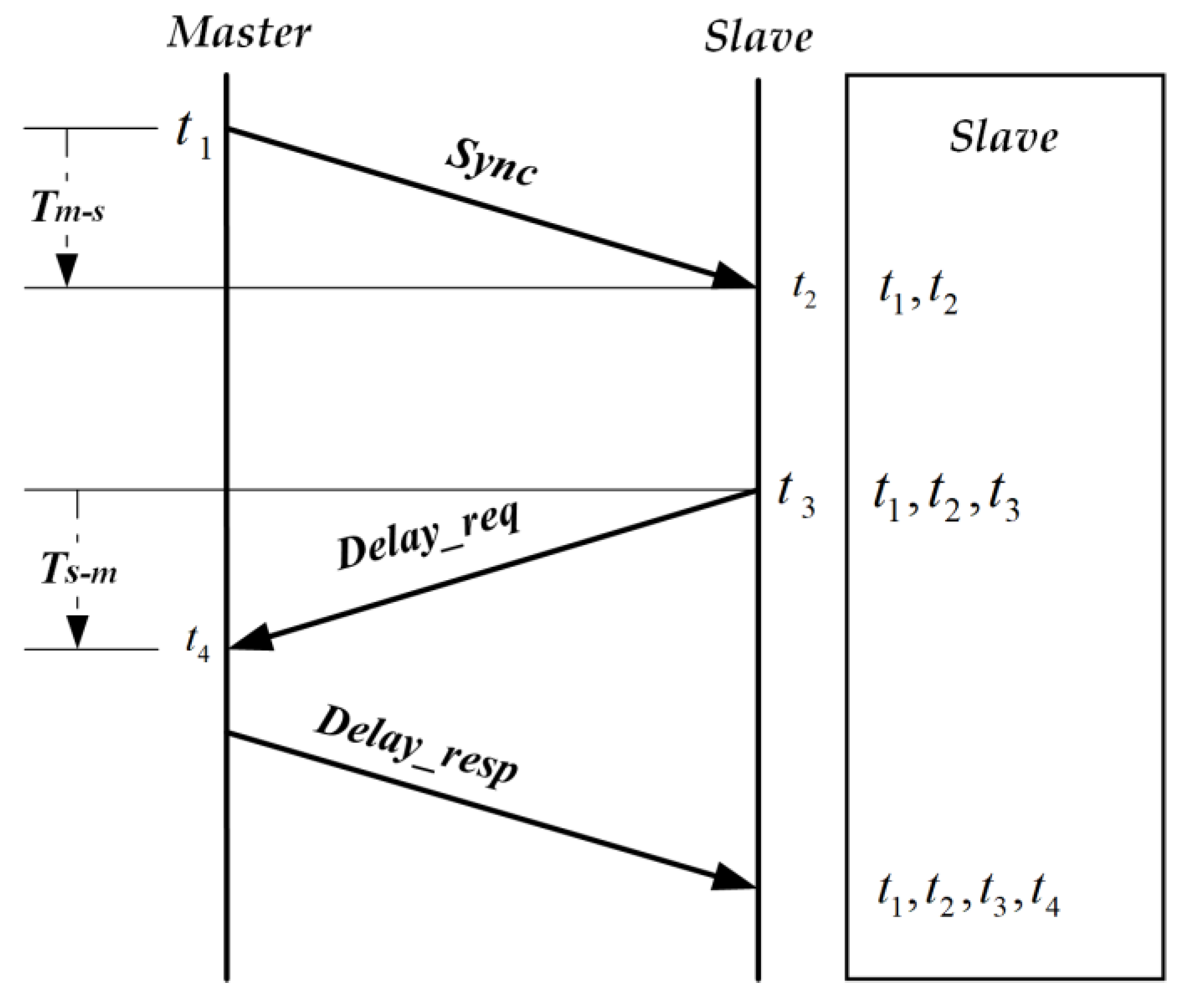
3.1. Precision Time Protocol Overview

The PTP is a protocol for Ethernet that enables time synchronization with sub-microsecond accuracy in a local area network (LAN); it operates based on a master and slave hierarchy. Depending on periodically exchanging messages and calculating offsets, the slave clock is able to adjust its time consistently with the master clock.
The fundamental principle of the PTP synchronization method is shown in the Figure 1. When using the PTP one-step mode for time synchronization in the network, first of all, the master sends a Sync message which includes a timestamp t 1 indicating the time when the Sync message is sent. The slave records the receive time of the Sync message t 2 and extracts the previously noted timestamp t 1 . Subsequently, the slave then sends a Delay_Req message and records the timestamp t 3 when it is sent. When the master receives the Delay_Req message, it records the receive timestamp t 4 and sends a Delay_Resp message to the slave. The Delay_Resp message carries the timestamp t 4 which will be extracted by the slave. After the exchange of three messages between the master and slave, the slave has obtained four timestamps, t 1 ~ t 4 . Assuming the time offset between the master clock and slave clock is T o f f s e t , and the transmission delay of the Sync message and the Delay_Req message are T m s and T s m , the synchronization process can be derived in accordance with the PTP protocol.
According to the above process, we can obtain the relationships between the timestamps:
t 1 + T o f f s e t + T m s = t 2
t 3 T o f f s e t + T s m = t 4
If T m s is equal to T s m , the formula for calculating the time offset between the master clock and slave clock is
T o f f s e t = ( t 2 t 1 ) ( t 4 t 3 ) 2

3.2. The Method Proposed in This Paper

The FPGA interacts with the switch using a telemetry message and ACK message to obtain a set of information (including four timestamps). There are multiple interactions in each synchronization period, resulting in multiple sets of information. A mapping relationship (related parameters are stored in the FPGA registers) between the FPGA’s timestamp and the switch’s timestamp can be calculated through multiple sets of information. With the help of a mapping relationship, obtaining a timestamp on one device can result in obtaining the timestamp on another device at the same reference time, thus achieving time synchronization.
Referring to Figure 2, the subsequent section outlines the procedure for the exchange of packets.
Firstly, the FPGA sends a telemetry message to the switch, which includes an FPGA send timestamp  t 1 indicating the time when it will be sent.
Secondly, the switch receives the telemetry message from the FPGA, records the switch recv timestamp  t 2 , and extracts the timestamp t 1 contained within the message. The switch generates a response message called the ACK, and the message carries the switch send timestamp  t 3 recorded at the time of sending the ACK message as well as the timestamps t 1 and t 2 .
Finally, the FPGA receives the ACK message from the switch and records the FPGA recv timestamp  t 4 upon receipt of the message.
The frequency of the FPGA timestamp and the switch timestamp may not be the same. Moreover, there exists an offset between the two timestamps when they are not synchronized. There is a mapping relationship between the FPGA timestamp and the switch timestamp. After knowing the timestamp of one device, we can estimate the other device’s timestamp at the same time by using this relationship and can match the two timestamps to achieve time synchronization. Suppose that the frequency ratio and offset of the switch timestamp and FPGA timestamp is denoted as A and o f f s e t . At the Coordinated Universal Time (UTC) t U T C , the timestamp on the FPGA is t F , and the timestamp on the switch is t S ; their relationship can be expressed as follows:
t S = A × t F + o f f s e t
t F = 1 / A × ( t S o f f s e t )
In this formula, A and o f f s e t are important parameters to characterize the mapping relationship. By obtaining these two parameters, we can obtain the FPGA (or switch) timestamps at the same UTC corresponding to the switch (or FPGA) timestamps, which is called the mapped FPGA (or switch) timestamp. After obtaining the message, like in the PTP, the transmission delay can be expressed in the following formulas:
D e l a y F S = t 2 A × t 1 o f f s e t
D e l a y S F = t 4 × A t 3 + o f f s e t
When D e l a y F S is equal to D e l a y S F , we can conclude that
t 2 + t 3 = A × ( t 4 + t 1 ) + 2 × o f f s e t
However, the D e l a y F S is hardly equal to D e l a y S F in the practical network environment. A compensation value C is set to counteract the asymmetry delay part according to the actual situation, then
t 2 + t 3 + C = A × ( t 4 + t 1 ) + 2 × o f f s e t
In the above formula, if we obtain multiple sets of timestamps, the mapping of parameters A and o f f s e t can be estimated using the least square method. During each time synchronization period, the two devices to be synchronized exchange packets repeatedly to obtain N sets of timestamps t 1 , t 2 , t 3 , and t 4 . We define t 4 + t 1 as X and t 2 + t 3 + C as Y; the least square method is used to estimate the two mapping parameters A and o f f s e t . The estimation is deduced as
A ^ = i = 0 N 1 X i Y i N X ¯ Y ¯ i = 0 N 1 X i 2 N X ¯ 2
o f f s e t ^ = Y ¯ X ¯ × A 2
These mapping parameters are subsequently stored on the FPGA after their calculation is completed.
At the same UTC, the relationship between the mapped FPGA timestamp M F ( t ) on the FPGA and the real switch timestamp t 1 on the switch is
M F t 1 = 1 / A ^ × ( t 1 o f f s e t ) ^
And the relationship between the mapped switch timestamp M S ( t ) on the FPGA and the real FPGA timestamp t 2 on the FPGA is
M S t 2 = A ^ × ( t 2 + o f f s e t ) ^

3.3. Problems of Clock Synchronization

The clock of the device is constructed using a crystal oscillator, which is sensitive to environmental temperature fluctuation, aging, and various other factors. These influences can result in frequency drift of the oscillator. Over time, the accumulated drift tends to increase, leading to a greater offset between the master clock and slave clock, which significantly affects synchronization accuracy. To address this issue, we employ an offset adjustment strategy. The specific procedure is as follows: during the interval between two synchronization events, the adjustment for the offset is determined by the offset value variation between the current synchronization and the previous synchronization.

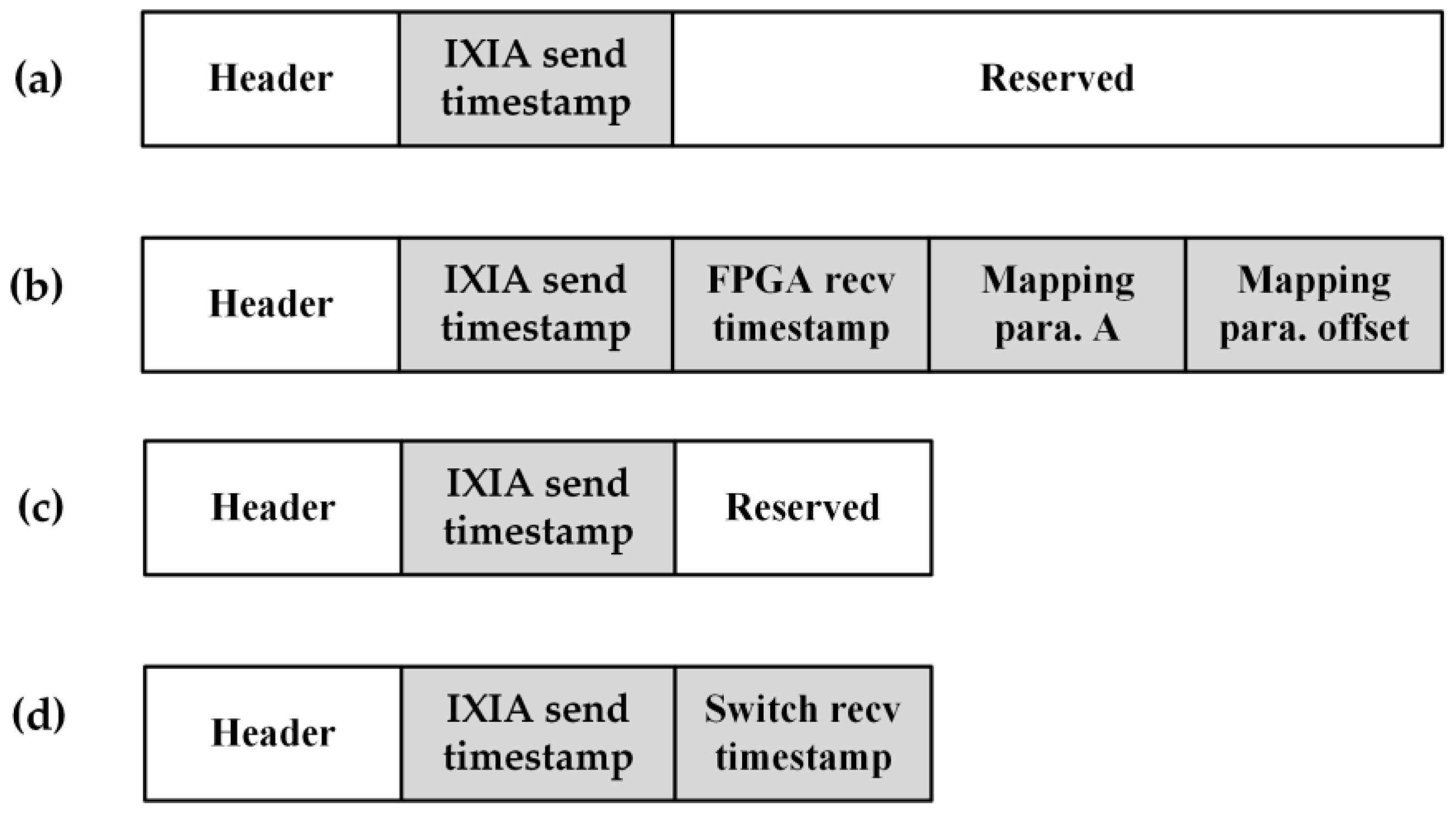
4. Design and Implementation

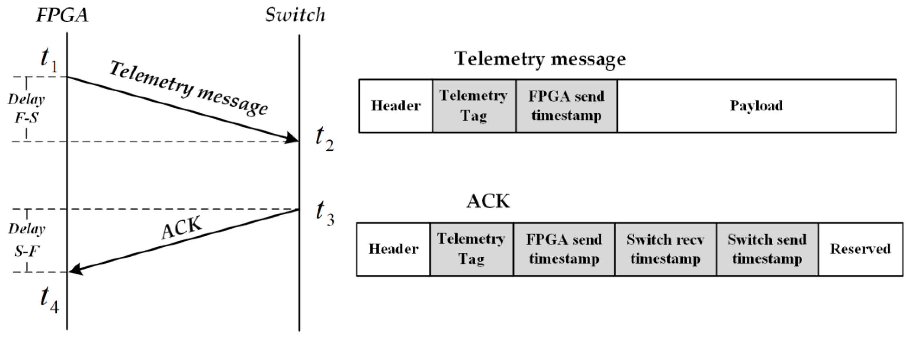
4.1. Implementation on an FPGA

To acquire the mapped timestamps from other devices on the FPGA, we have developed a hardware architecture on the FPGA that is shown in Figure 3. The design is implemented on a XILINX Zynq UltraScale+ ZU19EG FPGA.
The hardware architecture comprises a timestamp generator, a telemetry tagging module, a transmission (TX) timestamp insertion module, a reception (RX) timestamp insertion module, a calculation module located in the host, and a storage module.
During time synchronization, packets from other pipelines on the FPGA NIC firstly pass through the telemetry tagging module, where the packets are marked as telemetry packets. Then, the packets are sent to the TX timestamp insertion module and can be added with timestamp t 1 . After that, they are transmitted to the TX Ethernet port. The ACK packets coming from the RX Ethernet port are first added with timestamp t 4 in the RX timestamp insertion module; then, they are sent to the calculation module for timestamps parsing and the mapping parameters’ calculation.
The timestamp generator is used to generate the local FPGA timestamp. Its input is a 167 MHz pulse which is generated by PLL, and the output timestamp is derived from a 64-bit counter that counts the ticks since the initialization of the FPGA. The timestamp increments by one at the rising edge of each pulse, signifying that 6 nanoseconds of actual time has elapsed. The timestamp generator is connected to the RX timestamp insertion module and the TX timestamp insertion module.
The telemetry tagging module is user-configured to process data packets originating from the pipeline. This module selects data packets and tags them with telemetry information based on the configured synchronization period and the amount of packets of time synchronization in each period. A packet with added telemetry information becomes a telemetry packet. The telemetry information contains a tag field and a timestamp field, which are inserted into these selected packets. The packets are subsequently transmitted to the TX timestamp insertion module after being processed.
The TX timestamp insertion module adds the local timestamp into the designated positions in the telemetry packets according to the predetermined offset. Conversely, the RX timestamp insertion module adds the local timestamp into the ACK packets received from the switch and then sends them to the host.
The calculation module is situated on the host. It is responsible for receiving the ACK packets from the switch. It parses the timestamps ( t 1 ~ t 4 ) of each packet and then calculates the parameters A and o f f s e t of the timestamp mapping relationship. After the calculation is completed, it distributes the results to the storage module on the FPGA via the PCIe bus. The storage module, when necessary, provides the mapping parameters to other modules for one-way delay calculation. This module also incorporates an offset adjustment, which includes an internal timer that can be configured by the host. This configuration allows the host to decide how many clock cycles can adjust the offset by one.
We use Vivado 2020.2 for the work’s synthesis and implementation. The simulation tools used to run test benches are iverilog and cocotb. The maximal frequency for the FPGA circuit is 167 MHz after the place and route stage. The FPGA resource utilization and power consumption for the time synchronization modules are listed in Table 1 and Table 2.

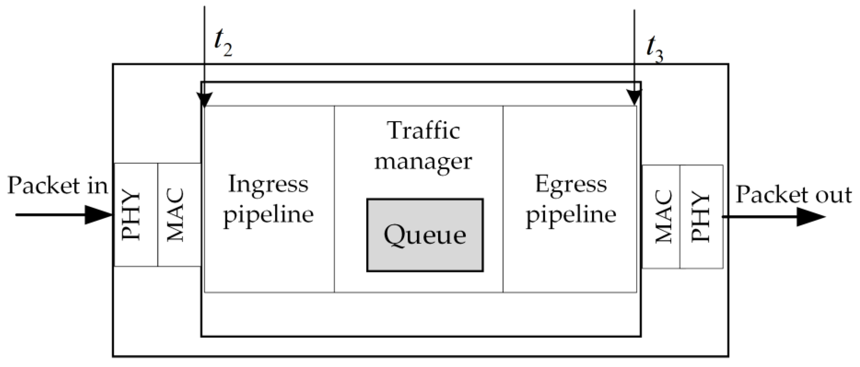
4.2. Implementation on Programmable Switch
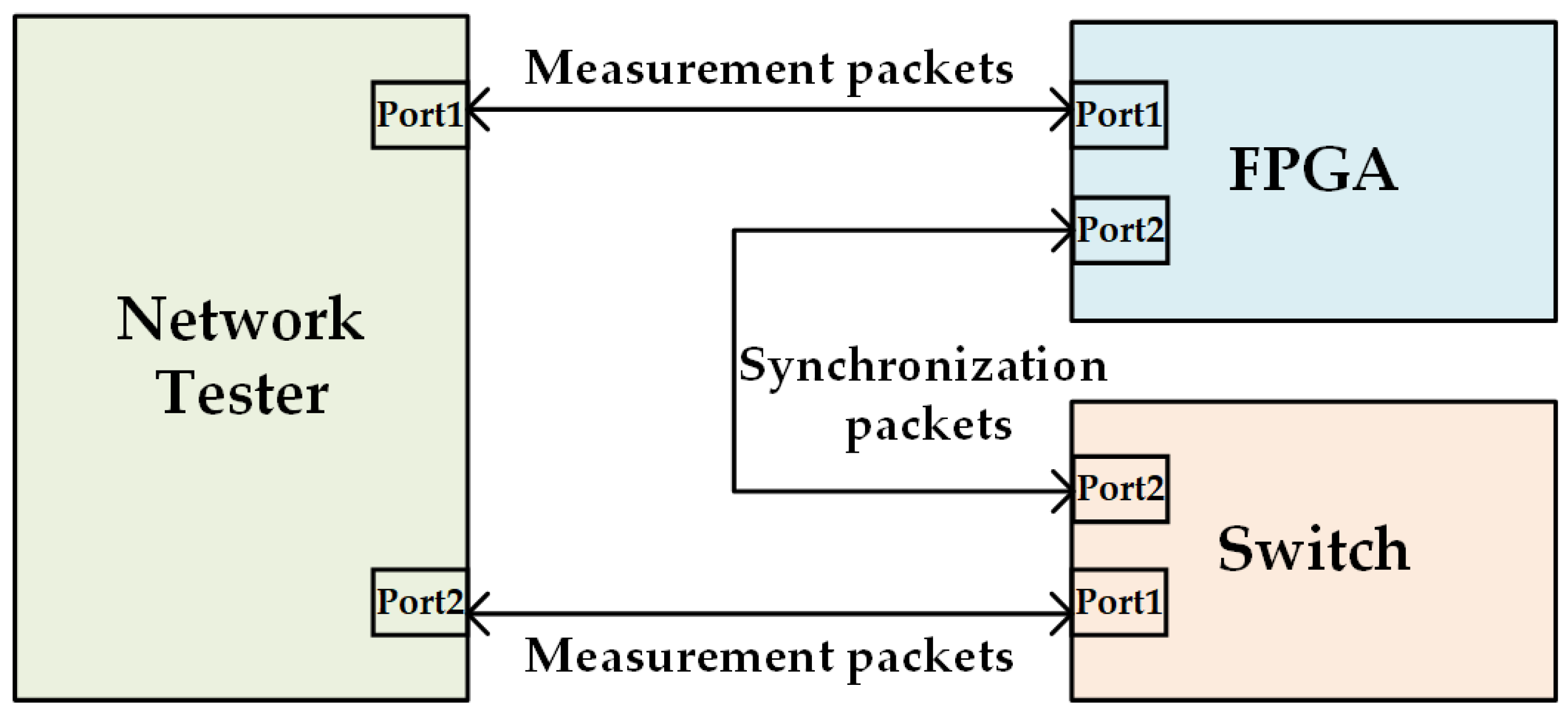
The process of telemetry messages is conducted on the Intel Tofino 1 platform [25]. Tofino is a pipelined chip that features data plane programmability. The Tofino 1 chip operates with a global clock frequency of 1.22 GHz. There is a Global Time Counter that consists of a 48-bit nanosecond component and a 28-bit fractional component. The Global Time Counter experiences a rollover approximately every three days. It disseminates time information to hardware blocks such as the MAC and Parser every 1 ns, which can be used to record the timestamps of packets in different process stages [26].
Tofino processes numerous packets that require being forwarded to their respective destinations. Upon receiving a packet containing telemetry information, the switch records the receive timestamp of packet t 2 in the data plane and resolves the timestamp t 1 from the original packet. Subsequently, it generates an ACK packet (a small size packet) that carries timestamps t 1 ~ t 3 and transmits it to the source FPGA.
Specifically, as shown in Figure 4, when receiving a telemetry packet, Tofino records the packet’s arrival time t 2 and parses the timestamp t 1 contained within the packet in the Ingress pipeline process. Both timestamps are stored in the metadata of the data plane. Subsequently, it triggers the mirroring function to generate a mirror packet that serves as an ACK packet, using t 1 ~ t 2 as the mirror header. After the mirror packet is generated, the Tofino populates the ACK packet, exchanges the source and destination IP addresses, and transmits the ACK packet to the loopback interface to reroute the routing pipeline. In the Egress pipeline, the send time t 3 is then appended in ACK packet.

5. Evaluation

To evaluate the proposed time synchronization method, we use a Network Tester IXIA-XGSHS to measure the synchronization error. IXIA-XGSHS is capable of generating multiple types of packets and recording the send and receive times of each packet. It has a more accurate and stable hardware timestamp than the FPGA and switch, so we considered the hardware timestamp of the Network Tester as the reference timestamp. Under the assumption that the synchronization approach is entirely accurate, the mapped switch timestamp calculated using the mapping parameters should correspond precisely to the actual timestamp on the switch at the same reference time. Consequently, we can interpret the discrepancy between the mapped timestamp and the actual timestamp as the synchronization error.
When the Network Tester transmits messages to the FPGA and the switch simultaneously, the messages will arrive at the FPGA and the switch at the same reference time after they traverse an equal length of optical fiber; thus, we can use the receive timestamps from the FPGA and the switch to calculate the synchronization error.
The Network Tester is interfaced with the FPGA and the switch via distinct ports. It periodically exchanges messages with two devices. The messages contain timestamps that indicate the send time and receive time as they traverse the three devices. Ultimately, these messages are received and captured by the Network Tester. Upon capturing the messages, the Network Tester analyzes the timestamps for further evaluation. Specifically, the accuracy and stability of the mapping relationship are assessed. The mapped switch time is computed using the mapping parameters and the FPGA timestamp included in the message from the FPGA. This computed mapped time is then compared to the actual switch timestamp present in the message from the switch, and the result difference is regarded as the synchronization error.
The three devices are interconnected as illustrated in Figure 5. The FPGA and switch communicate with messages transmitted over an optic fiber for the purpose of time synchronization. Concurrently, the Network Tester transmits measurement packets to both the FPGA and the switch. Following being processed by either the FPGA or the switch, the measurement packets are returned to the Network Tester. The block diagram depicting the FPGA’s process for the measurement packets is presented in Figure 6. This diagram incorporates shadow components into the original time synchronization architecture. The demultiplexer (demux) module on the FPGA will categorize the received packets into two distinct types: those used for time synchronization (telemetry packets and ACK packets) and those used for evaluation purposes (measurement packets). These packets will subsequently be directed to different modules for further process. The measurement packets are sent to the forwarding module. The multiplexer (mux) module aggregates two types of packets together and sends them to the TX timestamp insertion module. The function of the forwarding module is to relay the measurement packets from the receive pipeline to the send pipeline, which entails swapping the source and destination addresses, as well as appending two parameters, A and o f f s e t , in the storge module to specific locations within the packets. Additionally, measurement packets are added with a local timestamp at the RX timestamp insertion module upon their arrival at the FPGA. When the switch receives the measurement packets, it records the time at which the packets enter the pipeline. The formats of these messages are shown in Figure 7. The Network Tester captures the measurement packets returned from either the FPGA or the switch and extracts the local send timestamps contained within the packets, along with the timestamps received by the FPGA or switch. Furthermore, two mapping parameters are also extracted if the packets are from the FPGA.

6. Results

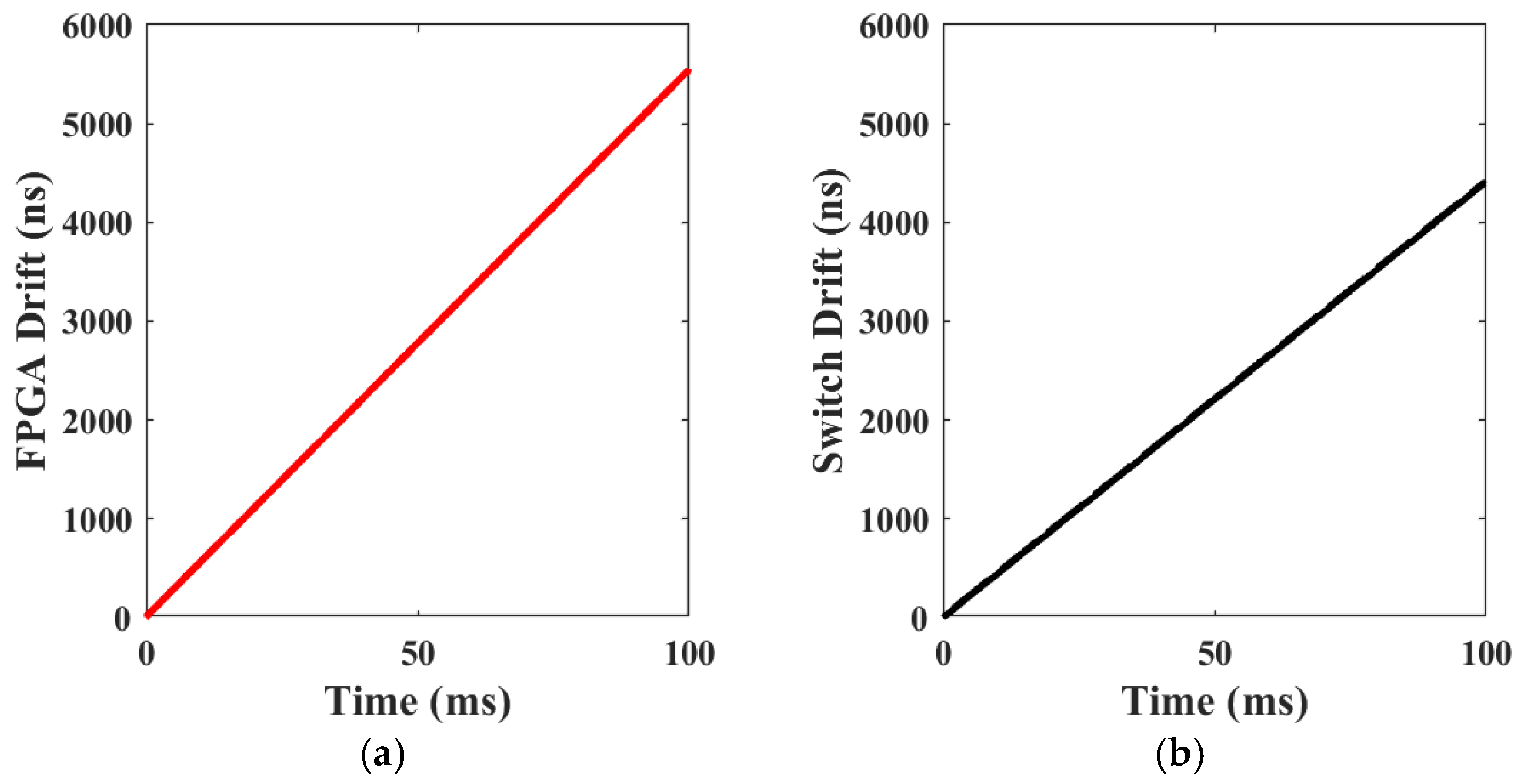
6.1. Clock Drift Measurement

Due to the issue of frequency drift associated with the device’s clock, we initially conducted measurements to assess the clock drift of both the FPGA and the switch. We employed a Network Tester to measure the degree of drift between the FPGA clock and the switch clock. The results are shown in Figure 8. The initial measurement indicated a clock drift of 0. The results demonstrated a linear relationship between clock drift and measurement time, revealing a drift of 5520 ns for the FPGA and 4300 ns for the switch over a duration of 100 ms, which corresponds to a clock drift rate of 55 PPM and 43 PPM.

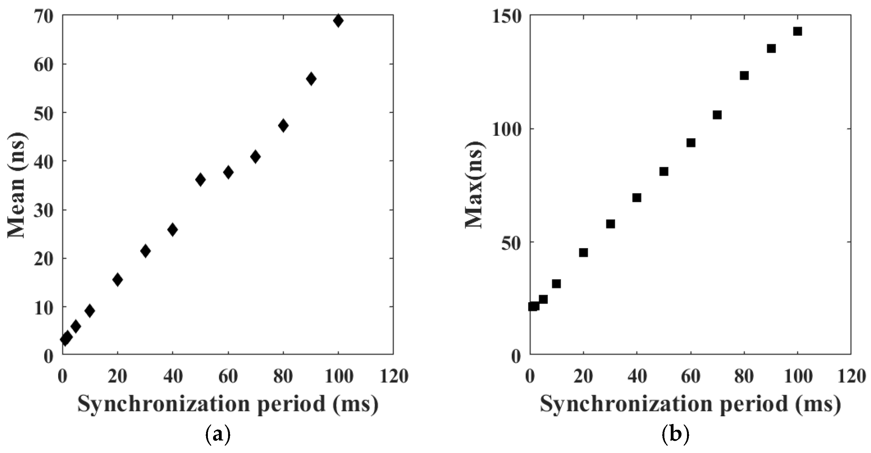
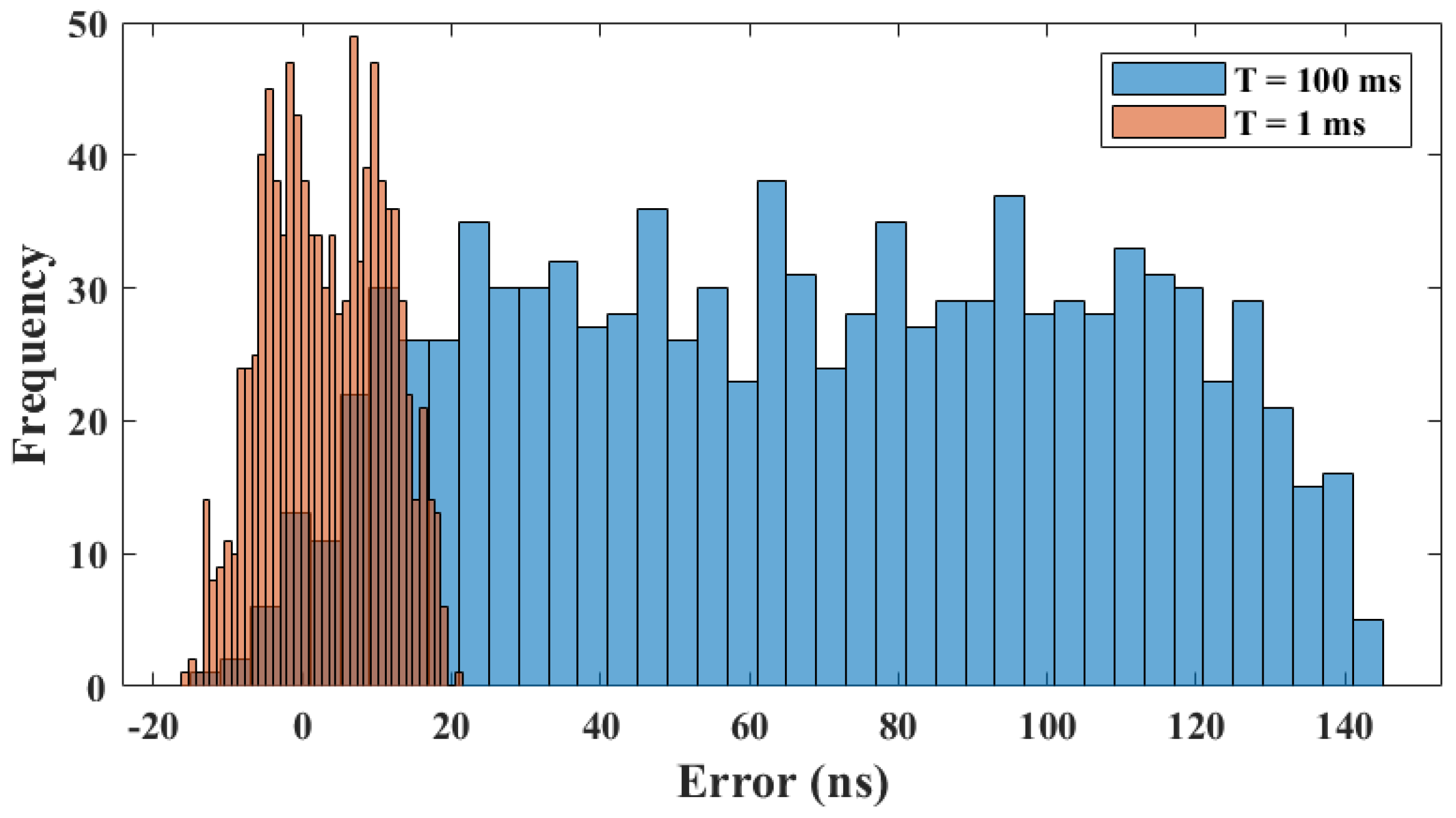
6.2. Time Synchronization Measurement

We employed a Network Tester to evaluate the accuracy and stability of time synchronization between the FPGA and the switch. It is assumed that the FPGA synchronizes its time with the switch over a period denoted as T, utilizing a total of 100 packets for each synchronization event. The Network Tester transmitted measurement packets to both the FPGA and the switch at intervals of 1 ms. The measurement time lasted for 1 s, resulting in a total of one thousand packets sent. The offset compensation C is set to 140 ns. Upon capturing the packets forwarded by the time synchronization devices, we analyzed the send timestamps from the Network Tester and the receive timestamps from the time synchronization devices, in addition to the mapping o f f s e t and mapping A in the packets from the FPGA. We calculated the discrepancy between the switch time derived from the mapping parameters and the actual switch timestamp. We conducted an analysis of the mean value, standard deviation, and the maximum values of the results obtained. We performed multiple measurements with synchronization period T from 1~100 ms; the results are shown in Table 3 and Figure 9 and Figure 10.
The results indicated that reducing the clock synchronization period from 100 ms to 1 ms leads to a decrease in the mean synchronization error from 69 ns to 3 ns, accompanied by a reduction in the standard deviation from 39 ns to 7.8 ns. Additionally, the maximum offset error decreased from 143 ns to 21 ns. This variation is due to the clock drift of the device’s crystal oscillator, whereby the synchronization error reaches its minimum at the moment when the mapping o f f s e t and mapping A are calculated and updated. Due to clock drift, the timestamp offset between two devices gradually increases while the mapping o f f s e t in the FPGA register remains unchanged in synchronization updating intervals, resulting in a large synchronization error until the next period register update. By shortening the synchronization period, the interval between two adjacent register updates is shortened, resulting in a smaller synchronization error and reduced jitter.
The distribution of the synchronization error also varies with different synchronization periods, which represents different degrees of stability. From the different results for T = 1 ms and T = 100 ms shown in Figure 10, it was evident that the concentration degree of the calculation results decreased with a longer synchronization period. When the synchronization period was 100 ms, the distribution of synchronization error values was scattered, ranging from -20 ns to 140 ns. In contrast, when the synchronization period was 1 ms, the calculation results were very accurate, and the distribution of error values was concentrated, with the error values mainly distributed between −20 ns and 20 ns. Therefore, it can be concluded that the stability increases with the shortening of the synchronization period.

6.3. Offset Adjustment

In Figure 11a, we observed the change in the mapping parameter o f f s e t on the FPGA at every time synchronization when the synchronization period was 1 ms and found that it showed a linear growth trend in a short time (at least 100 ms).
Figure 11. (a) Mapping parameter o f f s e t variation when synchronization period T = 1 ms; (b) synchronization results for period = 100 ms with offset adjustment.
Electronics 14 00610 g011
According to the aforementioned conclusions, if the mapping register is updated regularly without any intervention, it is necessary to synchronize time at shorter intervals to achieve higher time synchronization accuracy. However, the frequent transmission of time synchronization messages will lead to increased network overhead. To address the trade-off between network overhead or message process capability and synchronization accuracy, we propose an offset adjustment method. This method allows for the adjustment of the offset between the adjacent update intervals, thereby achieving a smaller synchronization error while extending the synchronization period. Based on the linear change in the offset in Figure 11a, we can make a prediction for the mapping parameter o f f s e t so as to adjust it. The procedure for predicting the offset is as follows: when the offset register is updated at the Nth time, the change between the current update value and the value from the previous update (N-1)th is calculated. This change is then evenly distributed across the two adjacent synchronization events’ time period, and an adjustment strategy is applied to the offset register of the FPGA. Specifically, the offset is increased by one for every specified number of clock cycles. The number of clock cycles is calculated by the software and delivered to the timer of the storage module. The results depicted in Figure 11b validated this method using a time synchronization period of 100 ms, resulting in synchronization performance with a maximum error of 19 ns and a standard deviation of 7.8 ns, which represented an 80% reduction in the standard deviation of the synchronization error with respect to the system without an offset adjustment. Furthermore, the maximum synchronization error was reduced by 86%.
In the above evaluation experiment, we achieved an accuracy of 19 ns with a synchronization period of only 100 ms. Table 4 gives a comparative analysis of the existing approaches and our proposed method. Comparing the performance of the method proposed in this paper with existing studies, the proposed method achieves higher accuracy using a longer synchronization period. It proves that we have obvious advantages, which indicated that the synchronization accuracy is 2~50 times higher than that of previous studies.

7. Conclusions

To solve the problem of high-precision time synchronization between devices in a datacenter, we proposed an innovative time synchronization method based on the timestamp mapping, which combines in-band telemetry to obtain the packet send and receive timestamps of the FPGA and switch. This paper introduced the principles and steps of the method and described the implementation of the method on an FPGA and programmable switch in detail. We also introduced the evaluation method and set up a test platform to evaluate the feasibility and effectiveness of the method. In the experiment, we studied the effect of the synchronization period on time synchronization performance and optimized the synchronization method by using an offset adjustment strategy. Finally, with a 100 ms time synchronization period and the offset adjustment strategy, the maximum synchronization error of this method is 19 ns, and the standard deviation is 7.8 ns; the synchronization accuracy is 2~50 times higher than that of previous studies. The proposed method achieves good time synchronization accuracy and stability and provides a new solution for the measurement of one-way delay in datacenters.

Author Contributions

Conceptualization, L.L. (Lei Liu); investigation and methodology, L.L. (Lin Li); software, L.L. (Lin Li) and B.C.; validation, L.L. (Lin Li), B.C. and D.D.; formal analysis, L.L. (Lin Li); writing—original draft preparation, L.L. (Lin Li); writing—review and editing, L.L. (Lei Liu) and D.D.; visualization, L.L. (Lin Li). All authors have read and agreed to the published version of the manuscript.

Funding

This work was supported by the Oriented Project Independently Deployed by Institute of Acoustics, Chinese Academy of Sciences: Research and Development of Key Technologies and Equipment for Low Latency Interconnection Network in Intelligent Computing Center Cluster (Project No. MBDK202401).

Data Availability Statement

The original contributions presented in this study are included in this article/Results. Further inquiries can be directed to the corresponding author.

Acknowledgments

The authors would like to thank Xinshuo Wang and Ao Zhang for providing technical assistance and insightful comments. The authors would like to sincerely thank the anonymous reviewers for their feedback on earlier versions of this manuscript.

Conflicts of Interest

The authors declare no conflicts of interest.

References

  1. Lei, Y.; Li, J.; Liu, Z.; Joshi, R.; Xia, Y. Nanosecond Precision Time Synchronization for Optical Data Center Networks. arXiv 2024, arXiv:2410.17012. [Google Scholar]
  2. Zhang, q.; Zhang, C.; Wang, J.; Tang, X.; Shen, Z.; Wang, H. Nanosecond level time synchronization in datacenter network based on Telemetry architecture. J. Commun. 2021, 42, 117–129. [Google Scholar]
  3. Bosshart, P.; Daly, D.; Gibb, G.; Izzard, M.; McKeown, N.; Rexford, J.; Schlesinger, C.; Talayco, D.; Vahdat, A.; Varghese, G.; et al. P4: Programming protocol-independent packet processors. ACM SIGCOMM Comput. Commun. Rev. 2014, 44, 87–95. [Google Scholar] [CrossRef]
  4. Kfoury, E.F.; Choueiri, S.; Mazloum, A.; AlSabeh, A.; Gomez, J.; Crichigno, J. A comprehensive survey on smartnics: Architectures, development models, applications, and research directions. IEEE Access 2024, 12, 107297–107336. [Google Scholar] [CrossRef]
  5. Kaur, S.; Kumar, K.; Aggarwal, N. A review on P4-Programmable data planes: Architecture, research efforts, and future directions. Comput. Commun. 2021, 170, 109–129. [Google Scholar] [CrossRef]
  6. Zhang, T.; Zhang, Q.; Lei, Y.; Zou, S.; Huang, J.; Li, F. Load balancing with traffic isolation in data center networks. Future Gener. Comput. Syst. 2022, 127, 126–141. [Google Scholar] [CrossRef]
  7. Bobda, C.; Mbongue, J.M.; Chow, P.; Ewais, M.; Tarafdar, N.; Vega, J.C.; Eguro, K.; Koch, D.; Handagala, S.; Leeser, M.; et al. The future of FPGA acceleration in datacenters and the cloud. ACM Trans. Reconfigurable Technol. Syst. 2022, 15, 1–42. [Google Scholar] [CrossRef]
  8. Verma, L.P.; Kumar, G.; Khalaf, O.I.; Wong, W.-K.; Hamad, A.A.; Rawat, S.S. Adaptive Congestion Control in IoT Networks: Leveraging One-Way Delay for Enhanced Performance. Heliyon 2024, 10, e40266. [Google Scholar] [CrossRef]
  9. Shin, M.; Park, M.; Oh, D.; Kim, B.; Lee, J. Clock synchronization for one-way delay measurement: A survey. In Proceedings of the Advanced Communication and Networking: Third International Conference, ACN 2011, Brno, Czech Republic, 15–17 August 2011; pp. 1–10. [Google Scholar]
  10. Chefrour, D. One-way delay measurement from traditional networks to sdn: A survey. ACM Comput. Surv. 2021, 54, 1–35. [Google Scholar] [CrossRef]
  11. Kannan, P.G.; Joshi, R.; Chan, M.C. Precise time-synchronization in the data-plane using programmable switching asics. In Proceedings of the 2019 ACM Symposium on SDN Research, San Jose, CA, USA, 3–4 April 2019; pp. 8–20. [Google Scholar]
  12. Crossley, P.A.; Guo, H.; Ma, Z. Time synchronization for transmission substations using GPS and IEEE 1588. CSEE J. Power Energy Syst. 2016, 2, 91–99. [Google Scholar] [CrossRef]
  13. Guo, H.; Crossley, P. Design of a time synchronization system based on GPS and IEEE 1588 for transmission substations. IEEE Trans. Power Deliv. 2016, 32, 2091–2100. [Google Scholar] [CrossRef]
  14. Mills, D. Internet time synchronization: The network time protocol. IEEE Trans. Commun. 1991, 39, 1482–1493. [Google Scholar] [CrossRef]
  15. Yuan, K.; Guo, X.; Tian, J. Research and implementation of clock synchronization technology based on PTP. J. Phys. Conf. Ser. 2021, 1757, 012139. [Google Scholar] [CrossRef]
  16. Vallat, A.; Schneuwly, D. Clock synchronization in telecommunications via PTP (IEEE 1588). In Proceedings of the 2007 IEEE International Frequency Control Symposium Joint with the 21st European Frequency and Time Forum, Geneva, Switzerland, 29 May–1 June 2007; pp. 334–341. [Google Scholar]
  17. Ferrant, J.-L.; Gilson, M.; Jobert, S.; Mayer, M.; Ouellette, M.; Montini, L.; Rodrigues, S.; Ruffini, S. Synchronous Ethernet: A method to transport synchronization. IEEE Commun. Mag. 2008, 46, 126–134. [Google Scholar] [CrossRef]
  18. Ferrant, J.-L.; Gilson, M.; Jobert, S.; Mayer, M.; Montini, L.; Ouellette, M.; Rodrigues, S.; Ruffini, S. Synchronous Ethernet and IEEE 1588 in Telecoms: Next Generation Synchronization Networks; John Wiley & Sons: Hoboken, NJ, USA, 2013. [Google Scholar]
  19. Lee, K.S.; Wang, H.; Shrivastav, V.; Weatherspoon, H. Globally synchronized time via datacenter networks. In Proceedings of the 2016 ACM SIGCOMM Conference, Florianópolis, Brazil, 22–26 August 2016; pp. 454–467. [Google Scholar]
  20. Moreira, P.; Serrano, J.; Wlostowski, T.; Loschmidt, P.; Gaderer, G. White rabbit: Sub-nanosecond timing distribution over ethernet. In Proceedings of the 2009 International Symposium on Precision Clock Synchronization for Measurement, Control and Communication, Brescia, Italy, 12–16 October 2009; pp. 1–5. [Google Scholar]
  21. Serrano, J.; Lipinski, M.; Wlostowski, T.; Gousiou, E.; van der Bij, E.; Cattin, M.; Daniluk, G. The white rabbit project. In Proceedings of the 2nd International Beam Instrumentation Conference, Oxford, UK, 16–19 September 2013. [Google Scholar]
  22. Rafii, A.; Sun, W.; Chow, P. Pharos: A multi-FPGA performance monitor. In Proceedings of the 2021 31st International Conference on Field-Programmable Logic and Applications (FPL), Dresden, Germany, 30 August–3 September 2021; pp. 257–262. [Google Scholar]
  23. Yin, H.; Fu, P.; Qiao, J.; Li, Y. The implementation of IEEE 1588 clock synchronization protocol based on FPGA. In Proceedings of the 2018 IEEE International Instrumentation and Measurement Technology Conference (I2MTC), Houston, TX, USA, 14–17 May 2018; pp. 1–6. [Google Scholar]
  24. Kyriakakis, E.; Sparsø, J.; Schoeberl, M. Hardware assisted clock synchronization with the ieee 1588-2008 precision time protocol. In Proceedings of the 26th International Conference on Real-Time Networks and Systems, Chasseneuil-du-Poitou, France, 10–12 October 2018; pp. 51–60. [Google Scholar]
  25. Grölle, D.; Schulz, L.-C.; Wehner, R.; Hausheer, D. Poster: High-Speed Per-Packet Checksums on the Intel Tofino. In Proceedings of the 6th on European P4 Workshop, Paris, France, 5–8 December 2023; pp. 49–52. [Google Scholar]
  26. Franco, D.; Zaballa, E.O.; Zang, M.; Atutxa, A.; Sasiain, J.; Pruski, A.; Rojas, E.; Higuero, M.; Jacob, E. A comprehensive latency profiling study of the Tofino P4 programmable ASIC-based hardware. Comput. Commun. 2024, 218, 14–30. [Google Scholar] [CrossRef]
  27. Kong, Y.; Wu, J.; Xie, M.; Yu, Z. A new design for precision clock synchronization based on FPGA. In Proceedings of the 2009 16th IEEE-NPSS Real Time Conference, Beijing, China, 10–15 May 2009; pp. 411–414. [Google Scholar]
Figure 1. The fundamental principle of the PTP synchronization method.
Electronics 14 00610 g001
Figure 2. The principle of the proposed method and the information in the messages.
Electronics 14 00610 g002
Figure 3. Structure of the FPGA-based time synchronization implementation.
Electronics 14 00610 g003
Figure 4. Structure of Tofino switch.
Electronics 14 00610 g004
Figure 5. Device connection diagram for evaluation.
Electronics 14 00610 g005
Figure 6. The block diagram of the FPGA for the measurement packets process.
Electronics 14 00610 g006
Figure 7. Measurement packets’ formats. (a) IXIA to FPGA; (b) FPGA to IXIA; (c) IXIA to switch; (d) switch to IXIA.
Electronics 14 00610 g007
Figure 8. The clock drift of the FPGA and switch. (a) The clock drift of the FPGA; (b) the clock drift of the switch.
Electronics 14 00610 g008
Figure 9. Synchronization results for various periods. (a) Mean value of offset error. (b) The maximum offset error.
Electronics 14 00610 g009
Figure 10. Synchronization results histogram for period T = 100 ms and period T = 1 ms.
Electronics 14 00610 g010
Table 1. FPGA resource utilization for time synchronization modules.
ModulesLUTRegistersBRAMCARRY8
Telemetry tagging221757598.57
TX timestamp insertion179012540288
RX timestamp insertion189712400336
Timestamp generator20126400
Storage18510000
Others (mux/demux et al.)1369401814
Total9470124359.5635
Table 2. Power consumption for time synchronization modules.
ModulesPower Consumption (W)
Telemetry tagging0.101
TX timestamp insertion0.037
RX timestamp insertion0.028
Timestamp generator0.013
Storage0.003
Others (mux/demux et al.)0.097
Total0.279
Table 3. Results for various synchronization periods.
Synchronization Period (ms)Mean (ns)Std (ns)Max_Error (ns)
13.257.8821
23.767.9121
55.998.0824
109.188.6831
2015.6110.9345
3021.5014.1757
4025.8217.1269
5036.1720.7681
6037.6722.5693
7040.9127.62106
8047.3733.23123
9056.9437.45135
10068.9639.36143
Table 4. Performance comparison against the state-of-the-art.
ApproachPlatformSynchronization PeriodAccuracy (ns)
Yuan et al. [15]STM32 MCU/1 μs
Kong et al. [27]FPGA/200 ns
Eleftherios et al. [24]FPGA0.5 ms138 ns
Yin et al. [23]FPGA/40 ns
Pharos [22]FPGA10 ms40 ns
Proposed ApproachFPGA100 ms19 ns
Disclaimer/Publisher’s Note: The statements, opinions and data contained in all publications are solely those of the individual author(s) and contributor(s) and not of MDPI and/or the editor(s). MDPI and/or the editor(s) disclaim responsibility for any injury to people or property resulting from any ideas, methods, instructions or products referred to in the content.

