1. Introduction
Spatial spectral filters, also known as frequency-selective surfaces (FSSs), are essential in numerous applications, including wireless communications, biomedical detectors, image sensors, atmospheric sciences, and various other fields [
1,
2,
3]. Filters take full advantage of the frequency response characteristics of circuit components to carry out the filtering of signals at specific frequencies. However, traditional filters often have disadvantages such as relatively bulky physical sizes, limited bandwidth flexibility, and significant insertion losses. Metasurfaces (MSs) can be deemed as the two-dimensional (2D) planar manifestation of metamaterials (MMs), and they have attracted considerable attention owing to their ultra-thin profile, low-profile attributes, and remarkable ability to manipulate EM waves [
4,
5]. MSs have been widely employed in the creation of a range of functional devices [
6], including absorbers [
7,
8,
9,
10], reflectors [
11,
12], retroreflectors [
13], metalenses [
14], wavefront manipulators [
15], filters [
16,
17,
18,
19,
20,
21,
22], and various other devices [
23,
24,
25,
26,
27,
28,
29,
30]. In particular, spatial MS filters (MSFs) have garnered increasing attention across an extensive spectrum of frequencies, covering microwaves, THz, and even higher optical frequencies within, owing to their exceptional spectral-filtering capabilities [
16,
17,
18,
19,
20,
21,
22,
27,
28,
29,
30,
31,
32,
33]. For example, Zhu et al. proposed a multiband spatial angular MSF with multiple hierarchical structures, capable of achieving a multiband operational mode while exhibiting spatial angular filtering performance [
18]. Yoshikawa et al. presented a novel methodology for bandpass MSFs that leverages circuit theory, allowing for functioning at the targeted refraction angle [
31]. Li et al. proposed a straightforward design for a bandpass MSF with a cross-shaped periodic array placed between two identical layers of four-square patches and dielectric substrates, enabling broadband and high transmission performance within the K
u band [
34]. However, these MSFs only respond and operate effectively for normal incident planar continuous waves (CWs); they are unable to respond to other waveforms, such as short pulse waves (PWs). In modern practical applications, it may be necessary to absorb or reflect certain signals (such as high-power short PWs), to avoid interference, while simultaneously transmitting or reflecting other signals (such as CWs) at the same frequency for antenna communication [
35,
36]. For the current most MSFs, the complexity increases when multiple signals share the same frequency, as frequency dependence can no longer be leveraged for their discrimination.
To address this issue, Wakatsuchi et al. introduced a novel approach that employs nonlinear circuit–based structures known as waveform-selective MSs, which exhibit the controlled absorption and transmission characteristics for surface PWs or CWs [
37,
38]. These waveform-selective MSs consisted of a metal resonator structure integrated with a nonlinear circuit that incorporated Schottky diodes, along with supplementary circuit components such as resistors configured in parallel with capacitors or in series with inductors [
39]. By leveraging the rectification properties of the four Schottky diodes on the incoming signal, these MSs demonstrated the capability to selectively absorb either short PWs or CWs, and selectively absorb or transmit specific waveforms [
40,
41]. Since its inception, the waveform-selective concept has provided an additional layer of control over the modulation of reflection or transmission behavior for incident EM signals with different waveforms that share the same frequency [
41,
42,
43,
44,
45,
46,
47,
48]. Waveform-selective MSs based on a nonlinear circuit have become a novel platform to construct various functional devices, such as filters [
42], cloaks [
43], antennas [
36,
44], and absorbers [
37,
38,
39,
40,
41,
46,
47]. However, the majority of current research on nonlinear circuit–based MS devices [
35,
36,
37,
38,
39,
40,
41,
42,
43,
44,
45], particularly focusing on MSFs, primarily concerns the selection of specific waveforms at a single frequency. Consequently, there is a growing requirement for the design and implementation of MSFs capable of independently distinguishing waveforms at two or more disparate operational frequencies.
In this work, we introduce a novel design of a dual-band MSF for transmitting CWs while inhibiting short PWs, which leverages a complementary cross resonator (CSR) structure mounted on a dielectric substrate and integrated with capacitive type nonlinear circuits. By connecting additional capacitors in parallel, the designed MSF can realize a waveform-selective filtering effect at two different and independent frequencies. Specifically, the designed MSF can transmit most of the CWs at both operating frequencies and simultaneously suppress the transmission of short PWs at the same frequencies. The designed MSF has excellent filtering performance in both dual frequency bands, and the difference in transmittance between CWs and PWs at the two frequencies of 2.0 GHz and 3.45 GHz is higher than 90%. In addition, we perform an in-depth discussion on the influence of incident PWs and CWs with different powers on the filtering performance of the MSF, as well as the influence of the oblique incidence angles under TE and TM modes on the filtering performance of the MSF. Subsequently, a systematic investigation is conducted into how RC circuit parameters affect the transmittance of CWs and PWs of the designed dual-band MSF. Our study lays a theoretical foundation for further research on MSFs and provides a prospective solution to the challenges associated with multifrequency waveform identification and filtering, which is expected to realize advanced waveform modulation and signal processing functions in low-frequency application fields such as antenna and wireless communication [
35,
36].
2. Design and Simulation
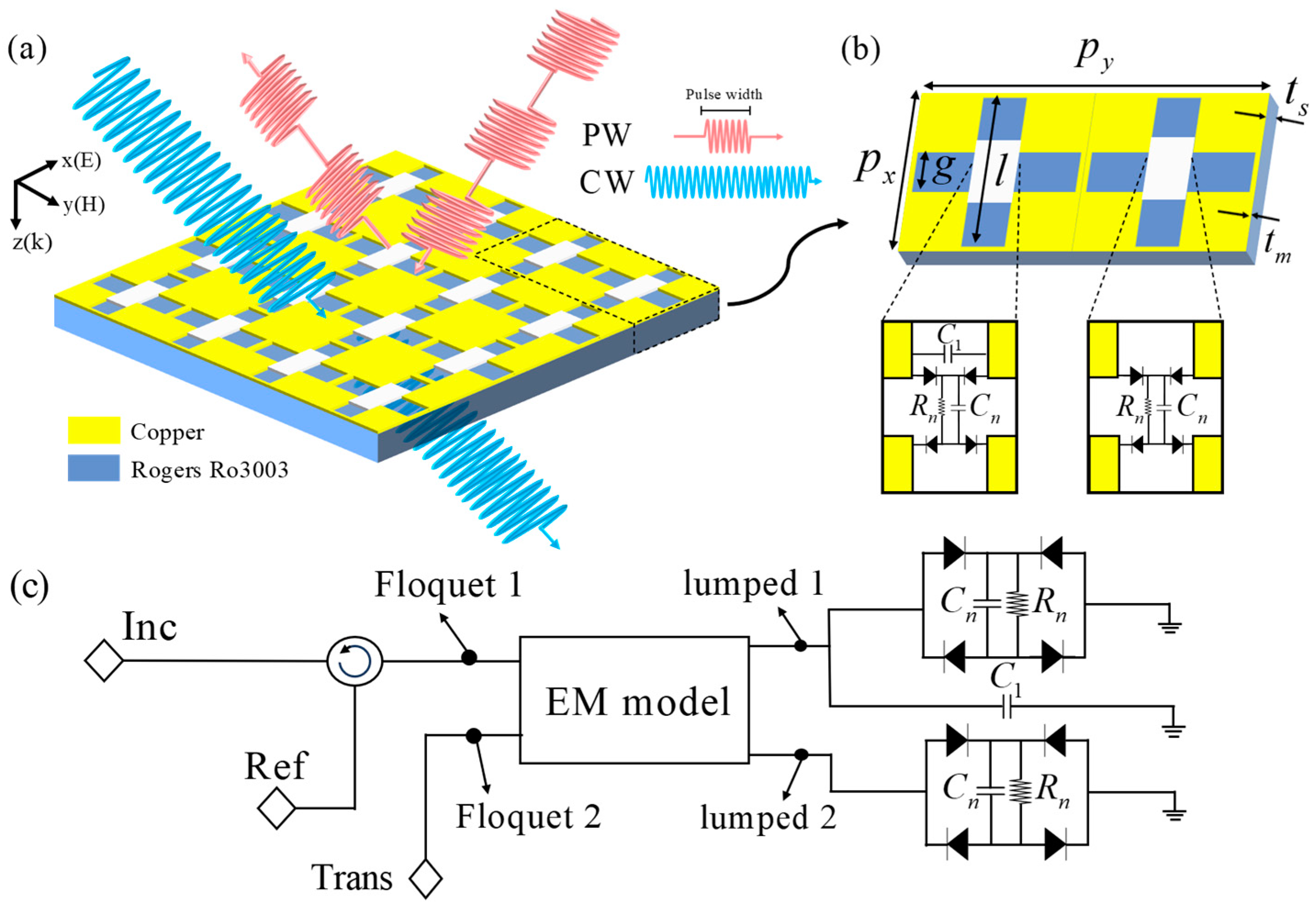
Figure 1 presents the schematic diagram of the designed MSF and its corresponding circuit simulation configuration.
Figure 1a depicts the 2D periodic array of the MSF, with its unit cell comprising two CSR structures adhered to a dielectric layer. The dielectric layer is a lossless polyimide substrate made of Rogers RO3003, with a relative permittivity of 3.0. As shown in
Figure 1b, the capacitive nonlinear circuit contains four Schottky diodes (forming one diode bridge) loaded with resistors (
Rn) and capacitors (
Cn) in parallel, respectively, positioned in the inner gaps of the two CSR structures (see the white rectangular region). To achieve two distinct resonance responses within the unit cell of the designed MSF, one of the capacitive nonlinear circuits is configured in parallel with a capacitor (
C1) within one CSR structure. This MSF structure was usually accurately modeled using a transmission line representation connected to an equivalent capacitive component
C0 and an equivalent inductive component
L0. The values of
C0 and
L0 were determined by the gap between the conducting patches and the substrate thickness, respectively [
44,
48]. Thus, the resonant frequency
f0 of the structure can be estimated by
. However, as illustrated in
Figure 1b, the resonance frequency
f0 can be readily adjusted by incorporating an additional lumped
C1, e.g.,
. It is expected that the introduction of another paralleled capacitor (
C1) can realize dual-band operation of the designed MSF. Here,
px and
py denote the period of a unit cell structure;
g and
l denote the width and length of the CSR gap, respectively;
ts represents the thickness of the dielectric substrate; and
tm indicates the thickness of the metal resonator.
In this design, the electric field of the incoming EM waves with a certain power, which is normal to these nonlinear-circuit CSR structures, charges the inner edge of each CSR either positively or negatively, resulting in a high induced voltage across the gaps within the CSR array. Consequently, the set of four diodes effectively rectifies the incoming EM wave signal into a stationary field across these gaps through Fourier transformation [
38]. Specifically, full-wave rectification using a diode set bridge is more efficient at converting the incoming wave signal into a DC component compared to half-wave rectification with a solitary diode [
39,
40]. The capacitive nonlinear circuit is more effective at suppressing short PWs while absorbing CWs at the same frequency less effectively. This is due to the ability of the parallel capacitors to temporarily store the rectified EM energy, which gradually charges up as a result of the zero-frequency component. The rectified EM energy can be regulated by the time constants of the other components,
RnCn. Consequently, the filtering performance of the designed capacitive nonlinear-circuit MSF highly depends on the pulse width of the incoming EM wave signals.
To demonstrate the waveform-selective filtering properties at the two distinct frequencies, the transmission properties of the designed capacitive-type nonlinear-circuit MSF were calculated using a co-simulation within ANSYS Electronic Desktop (version 2022). This integrated platform combined an EM simulator (HFSS) with a circuit simulator (Circuit) to facilitate the analysis. In the EM simulation, the master–slave boundary conditions are employed, and the size of mesh dissection is set to 0.0001 mm, two Floquet ports were utilized to launch an incident wave and observe the reflected and transmitted waves. Lumped ports replaced all circuit components (represented as the white rectangular areas of the 2D array in
Figure 1a), which were positioned at the gaps of the metallic CSR structure. The lumped ports were interfaced with the circuit components within the simulator. In the EM simulation, the optimized structural parameters of the unit cell are as follows:
px = 32 mm,
py = 64 mm,
l = 30 mm,
g = 8 mm,
ts = 3.5 mm, and
tm = 0.017 mm. In the circuit simulation, the Schottky diodes from the HSMS-286x series by Avago were modeled using the SPICE model, and the pertinent parameters are provided in Ref [
43]. The resistance and capacitance of these parallel-connected chip resistors (
Rn) and capacitors (
Cn) were
Rn = 300 KΩ and
Cn = 1 nF. Thus, the time constant of this capacitive type nonlinear circuit is
τ =
RnCn = 300 μs. All the results can be obtained by connecting the circuit components with the MSF circuit models. During the circuit simulation, a scan is carried out at a step length of 0.05 GHz within the frequency range from 1 GHz to 5 GHz. It is worth noting that the short PWs discussed here are sine wave-modulated pulses. When the pulse width is excessively short, the modulated waveforms will contain frequency components in addition to the excitation frequency. To mitigate this issue, a pulse width of 50 ns is utilized for the short PWs in this study [
45]. The CWs employ sine planar waves, and both waveforms share the same frequency and power. Consequently, the transmittance of nonlinear circuit–based MSFs in the time domain was calculated in the following manner:
where
Pt and
Pi represent the transmitted power and the incident power, respectively. For the PWs,
t1 was set to 0 seconds and
t2 was established as the end of the pulse duration plus an additional 50 ns. Regarding CWs,
t1 was selected during the steady state, whereas
t2 was designated as four cycles after
t1. The transmittance was calculated using the circuit simulator.
3. Results and Discussion
Firstly, as shown in
Figure 2a, we consider the single-band waveform-selective filtering performance of the designed MSF with two additional identical paralleled capacitors (
C1).
Figure 2b,c presents the simulated transmittance of the designed MSF with different values of
C1 for the normal incident 50 ns short PWs and CWs both with 10 dBm power. As shown in
Figure 2b, for the normal incident PWs, the transmittance of the designed MSF is nearly unchanged and below 10% across the entire interested frequency range (1–5 GHz) when changing the value of
C1. However, for the normal incident CWs, the designed MSF exhibits strong transmissivity in the single-band when the value of
C1 changes, as shown in
Figure 2c. Furthermore, the transmittance is nearly unchanged and greater than 95% while the operation frequency will gradually shift toward the lower frequency region as the paralleled
C1 increases due to the increase in the equivalent capacitance of the MSF.
Specifically, when C1 increases from 0 pF to 0.6 pF, the frequency point of the transmission peak of the CWs shifts from 3.05 GHz to 1.75 GHz, and the full width at half maximum (FWHM) of the transmittance is decreased from 1.05 GHz to 0.3 GHz. This verifies that the designed MSF with two additional identical parallel capacitors C1 can achieve a strong CWs transmissive property while inhibiting PWs within a single band. The above results prove that the single-band MSF has an excellent waveform-selective filtering effect and the operation frequency can be regulated by altering the value of parallel capacitor C1. It is inspired that the dual/multiband waveform-selective filtering effect of the MSF can be realized by integrating two/more additional different parallel capacitors into the nonlinear-circuit structure.
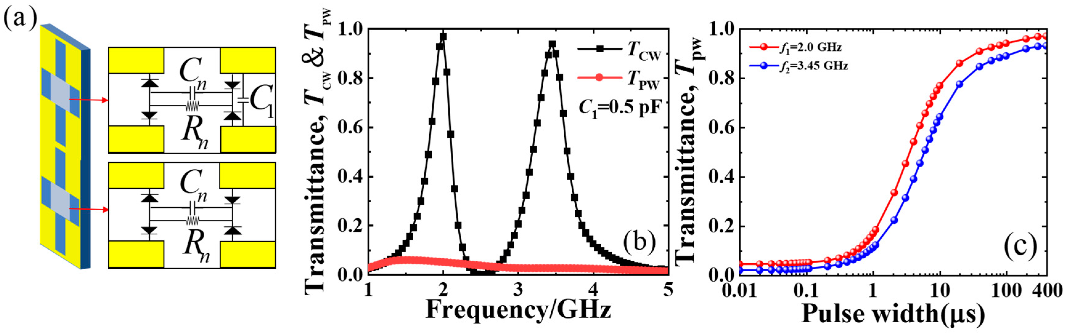
Without loss of generality, we construct a dual-band MSF by integrating a capacitive nonlinear circuit with the paralleled
C1 into one CSR structure, as shown in
Figure 3a. In this designed dual-band MSF, the
C1 is set to 0.5 pF, and the corresponding transmittance for the normal incident CWs and PWs is depicted in
Figure 3b. The MSF has a transmittance of up to 97% and 94% at 2.0 GHz and 3.45 GHz for CWs, respectively, while the one for the 50 ns short PWs is only 4.8% and 2.3%. Based on transmission line theory, it is conjectured that the response of this dual-band MSF at the lower frequency (2.0 GHz) is governed by a capacitive nonlinear circuit that includes the paralleled component
C1, whereas the response at the higher frequency (3.45 GHz) is determined by a different capacitive-type nonlinear circuit that does not include
C1. In addition, the transmittance of the 50 ns short PWs is below 6% across the entire interested frequency range of 1–5 GHz. Evidently, the proposed MSF has a remarkable ultra-broadband shielding performance for the short PWs.
Figure 3c presents the transmittance (
TPW) of the designed dual-band MSF for the normal incident PWs with different pulse widths at 2.0 GHz and 3.45 GHz, respectively. When the pulse width of the PWs increases from 50 ns to 400 μs, the transmittance of the designed dual-band MSF increases from 4.8% and 2.3% to 97.1% and 93.9% at 2.0 GHz and 3.45 GHz, respectively. It means that there is a distinct transition between the shorter and longer PWs with an input power of 10 dBm. This is mainly related to the time constant of the RC circuit. In this model, the time constant of the RC circuit is
τ =
RnCn = 300 μs. When the pulse width of the PWs gradually increases and reaches the time constant of the RC circuit, the long PWs then exhibit the characteristics of CWs. The long-time charging causes the energy storage performance of capacitor
Cn to decline and tend to saturation. Before the arrival of subsequent PWs, it cannot store and dissipate the current energy, thus leading to a gradual increase in transmittance with the increase in the pulse width of the incident pulse waves. This result further validates the dual-band selective transmittance characteristics of the designed MSF based on nonlinear circuits for specific pulse waveforms.
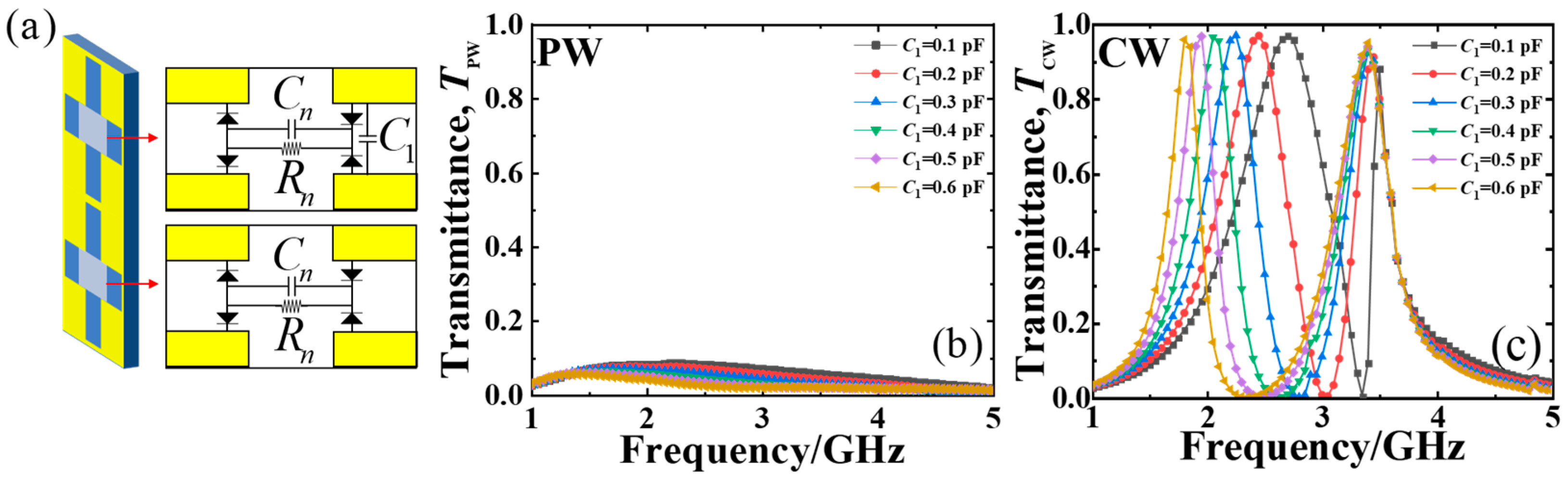
Next, we consider the influence of the different
C1 on the transmittance of the dual-band MSF for the normal incident PWs (50 ns) and CWs. As depicted in
Figure 4b, when changing the value of
C1, the transmittance of the 50 ns short PWs is below 9% across the entire interested frequency range of 1–5 GHz. Obviously, the designed MSF with different
C1 also has an excellent ultra-broadband shielding performance for the short PWs. As depicted in
Figure 4c, for normally incident CWs, the transmission peak at the lower frequency undergoes a red shift, whereas the higher frequency peak remains nearly unchanged as the value of
C1 increases. This is because the lower frequency response of this dual-band MSF is determined by a capacitive nonlinear circuit with the paralleled
C1, while the higher one without
C1. Thus, as the paralleled
C1 increases, the first frequency point will gradually shift toward the lower frequency region, while the second one is nearly unchanged. This means that the dual-band filtering function of the proposed MSF is achieved, and the operation frequency can be adjusted easily.
Taking a step further, we study the influence of the different input power, oblique incident angle of both TE and TM, and the parameters of paralleled capacitors (
Cn) and resistors (
Rn) on the waveform-selective filtering performance of the designed dual-band MSF (see
Figure 1b).
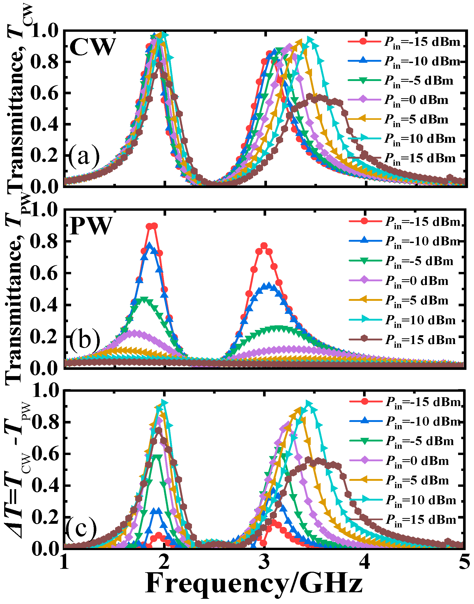
Figure 5 illustrates the influence of short PWs (50 ns) and CWs with different input powers on the waveform-selective filtering performance of the designed dual-band MSF. As depicted in
Figure 5a,b, when the input power increases from −15 dBm to 15 dBm, the transmittance peaks of the dual-band MSF for the normal incident CWs around 1.95 GHz and 3.45 GHz firstly increase and then decrease gradually, while the one for the short PWs decreases gradually.
As depicted in
Figure 5b,c, the corresponding transmittance difference (
△T =
TCW −
TPW) between CWs and PWs firstly increases gradually and then decrease slightly with the increase in the input power. At a low power of −15 dBm, the transmittance of both CWs and PWs is over 60%, and the transmittance difference between CWs and PWs is very small and only 5.1% and 2.3% around 1.95 GHz and 3.15 GHz. Under such conditions, the input power is extremely low, and the voltage induced by the incident CWs and PWs on the surface of the metal CSR structures falls below the threshold voltage of the rectified diodes, rendering the activation of the diodes for rectification impractical. Consequently, the transmittances for both CWs and PWs around these two frequencies are nearly the same. When the input power is increased to 10 dBm, the difference in transmittance between CWs and PWs around 1.95 GHz and 3.45 GHz attain their peak values of 92.3% and 91.6%, respectively. Under such circumstances, the induced voltage in CSR structures is sufficient for activating the rectification of the bridge diodes. The capacitive nonlinear circuits in the CSR structures significantly contribute to the robust suppression of transmission performance for short PWs and the enhancement of CWs at frequencies above this range. When the input power reaches 15 dBm, the transmittance for CWs is 69.6% and 58.4% around the above two resonance frequencies, while that for PWs reaches about 3.6% and 2.4%. In this scenario, the induced voltages generated by the PWs and CWs within the CSR structure surpass the voltage threshold for diode bridge breakdown, thus breaking down the diodes, resulting in a substantial suppression of the nonlinear transmission mechanism. Consequently, the transmission ability of MSF for CWs is weakened. Nevertheless, since the duration of the induced current formed by the high power PWs is too short, the energy can be easily dissipated or reflected by the wires and resistors in the RC circuit, and the MSF still maintains a low transmittance for the PWs. However, the transmittance difference between CWs and PWs is still over 50% when the input power is increased to 15 dBm. This means that the designed dual-band MSF has a significant selective filtering performance for the high power PWs.
Figure 6 presents the simulated transmittance (
TCW,
TPW) spectra of the dual-band MSF on different waveforms when the incident angle is varied under different polarization modes. As depicted in
Figure 6a,b, for the CWs with an incident angle changed from 0° to 60°, the transmittance of the dual-band MSF for both TE and TM modes is always higher than 90% around 2.0 GHz. However, around the higher frequency of 3.45 GHz, with the increase in incident angle, the transmittance of CWs for TE mode shows a decreasing trend and the resonant frequency points gradually diverge when the incident angle is over 35°. This is because when the TE mode is obliquely incident, the larger the incident angle is, the more the wave behavior resembles that of the TE surface wave. In this case, the EM wave has a strong electric field component, which enhances the rectification process of the diode. As a result, more incident waves are absorbed or reflected, leading to a decrease in the transmittance of CWs in the higher frequency. For the lower frequency, due to the presence of parallel diodes, part of the electric field component is shunted. Therefore, the obliquely incident CWs in the TE mode have little impact on the transmittance of the lower frequency. However, as shown in
Figure 6b for the higher frequency, multiple absorption peaks are observed for the CWs when the incident angle exceeds 35°, attributed to a reduction in the excitation of resonance modes associated with the electric field component. In addition, as depicted in
Figure 6b, when the incident angle of CWs for the TM mode is increased, the electric field component does not change significantly. Therefore, for the CWs obliquely incident in the TM mode, the transmittance at the two resonant frequency points remains at a relatively high level. It is worth noting that due to the higher-order resonances response, the resonance bandwidth of the transmittance near these two frequencies will be slightly broadened. As depicted in
Figure 6c,d, when the incident angle is changed from 0° to 60°, the transmittance of the dual-band MSF for both TE and TM mode PWs is always below 10%. This implies that the designed dual-band MSF has an excellent shielding performance in a wide-angle range for the short PWs, and also wide-angle transmission property for the CWs. From this, it can be concluded that the designed dual-band MSF possesses the characteristics of polarization insensitivity and certain wide-angle stability.
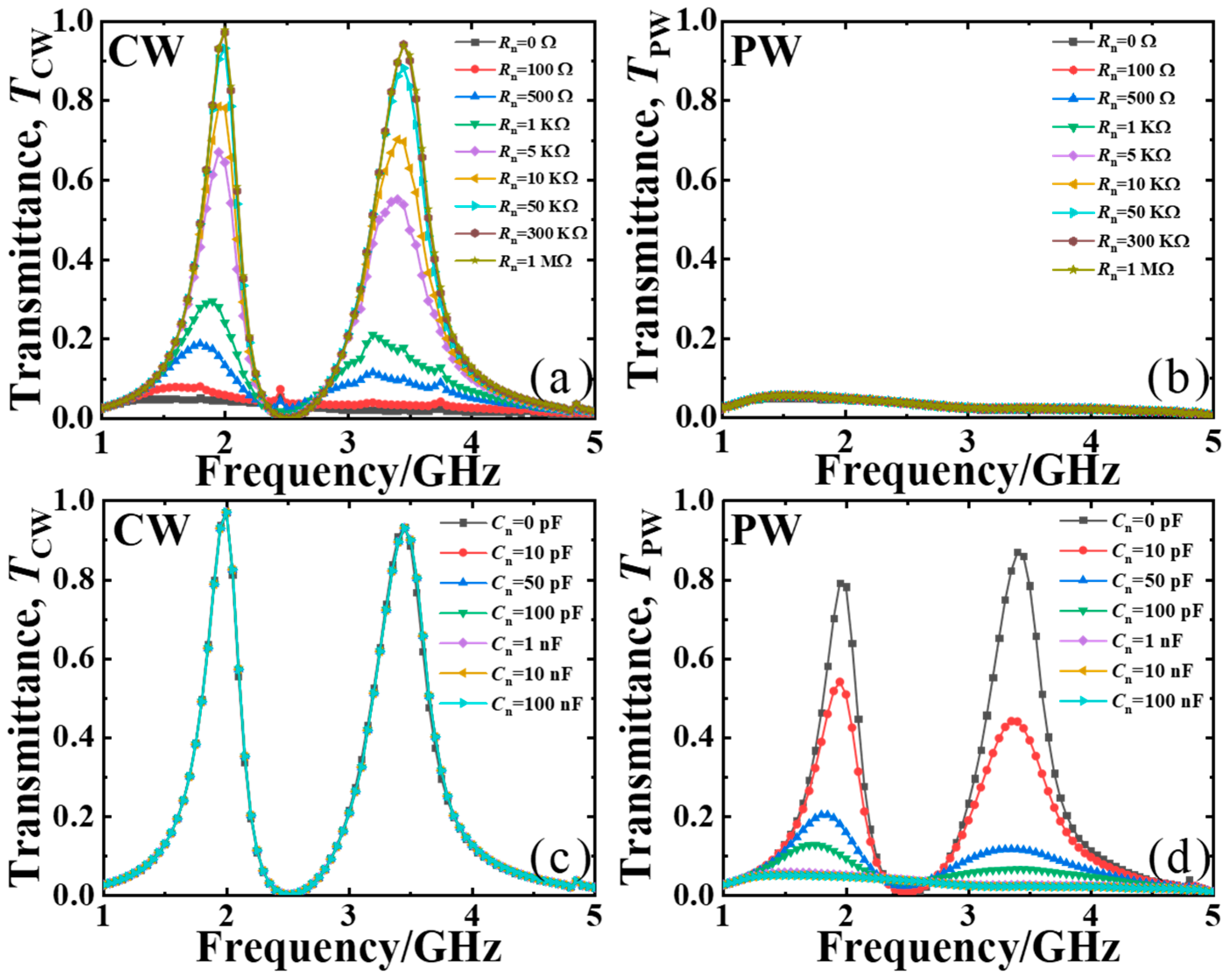
Finally, as depicted in
Figure 7, we studied the effect of the circuit component parameters (
Rn and
Cn) on the filtering characteristics of the dual-band MSF for both short PWs (50 ns) and CWs, both with an input power of 10 dBm.
Figure 7a,b present the transmittance spectra of the proposed dual-band MSF for the normal incident CWs and PWs with different
Rn while fixed
Cn = 1 nF in the nonlinear circuits. It can be observed that when the
Rn is less than 5 KΩ, the transmittance of the designed dual-band MSF for CWs is lower than 30%. This is because when
Rn is small, the equivalent impedance of the designed dual-band MSF is seriously mismatched with the free space, which finally leads to a considerably diminished transmission property for CWs. When
Rn reaches 300 KΩ, the transmittance of the proposed dual-band MSF for CWs can reach up to maximum values of 97.1% and 93.9% at 2.0 GHz and 3.45 GHz, respectively, indicating that the dual-band MSF must have a sufficiently large resistance to achieve its high transmittance for CWs. When changing
Rn, as depicted in
Figure 7b, the transmittance of the proposed dual-band MSF for PWs remains nearly unchanged and at an extremely low level. This is due to the fact that the energy of the electrostatic field generated by the incident PWs within the MSF is mainly dissipated through the internal resistance of the rectified diodes rather than the paralleled
Rn in the capacitive nonlinear circuit.
Figure 7c,d present the transmittance of the designed dual-band MSF for CWs and PWs with varied
Cn and fixed
Rn = 300 KΩ in the nonlinear circuits. As illustrated in
Figure 7c, it is evident that variations in
Cn do not affect the transmission of CWs, with the transmittance of CWs remaining consistent at 97.1% at 2.0 GHz and 93.9% at 3.45 GHz, respectively. This is due to the zero-frequency component generated by the diode bridge rectification completely charging the capacitor, which subsequently inhibits the absorption of CWs and ultimately enhances the transmission of CWs at above two frequencies. From
Figure 7d, with the continuous increase in the
Cn, the transmittance of the designed dual-band MSF for short PWs exhibits a significant decline, and it remains consistently below 6% once
Cn exceeds 1 nF. When
Cn < 1 nF, as
Cn increases, the time constant
τc =
CnRn progressively surpasses 50 ns, which is the pulse width of PWs, thereby impeding the transmission performance of PWs. When
Cn >1 nF, the transmittance of short PWs diminishes to 4.8% at 2.0 GHz and 2.3% at 3.45 GHz, respectively. This indicates that a larger
Cn can accumulate shorter PWs (50 ns) energy, rendering the transmission performance of the dual-band MSF for PWs greatly reliant on
Cn.


 ,
, 