1. Introduction
The upcoming Electron-Ion Collider (EIC) project [
1,
2], along with other next-generation accelerators [
3,
4], requires an ultrafast, high-voltage, high-current pulsed power supply to drive the kickers essential for ion injection into the collider ring. These kickers play a critical role in creating, accelerating, and shaping particle beams. The EIC will feature two intersecting accelerators: one producing an intense electron beam and the other generating a high-energy beam of protons or heavier atomic nuclei, which are steered into head-on collisions.
One section of the EIC beamline will require a hadron injection kicker system based on stripline kickers. These vacuum devices are driven by a pair of rectangular pulses with opposite polarities to provide transverse kicks to the bunched particle beam [
5]. The EIC injection kicker system must support single-bunch transfers at a bunching frequency of 24.6 MHz. Consequently, the kicker system must achieve rise, flat-top, and fall times totaling no more than 40.7 ns (for comparison, the current RHIC bunching period is approximately 107 ns [
6]). The entire system will include 20 kicker units, spanning a total length of ~25 m.
Table 1 summarizes the requirements for the fast kicker pulse generators planned for the EIC.
Traditionally, gas-discharge switches combined with pulse-forming networks [
7] were used to produce short pulses with nanosecond-scale edges. However, the limited stability of gas-discharge devices over time and temperature, along with their restricted service life, makes them unsuitable for modern systems. Semiconductor-based pulse generators, such as those using Si or SiC MOSFETs [
8], can meet these demands. However, the power output of a single device (a few kV and tens of amperes) is insufficient, necessitating circuit designs that combine multiple devices in series and parallel configurations to achieve the required voltage and current levels.
To further satisfy the downstream development of control circuits capable of providing high synchronization of operation and stability in time, maintaining a high switching speed and galvanic isolation for each switch is also required. In addition, it is necessary to resolve the issue of balancing the voltages and currents at the moment of switching and during the pulses, respectively, in order to ensure the reliable operation of the generator as a whole. An example of existing pulsers with specifications close to EIC requirements (at least in voltage and current amplitudes) was originated by Diversified Technologies, Inc. [
9]. They experimentally demonstrated the applicability of using MOSFETs to achieve <10 ns rise times for a 50 Ω load, but with a falling edge shape that shows noticeable ripples and is too long.
Another possible solution is based on a fast ionization dynistor (FID) [
10], which demonstrated successful operation at 50 kV with a 50 Ω load but showed a long fall time. While FIDs are powerful and versatile, they present several technical disadvantages: they require precise triggering to initiate avalanche breakdown and ensure intended switching. Any deviation in the triggering pulse can lead to delayed or premature firing, potentially damaging the device or other components. To achieve a short falling edge, pulse-forming networks are required, which restrict the system to a fixed pulse length. Additionally, the FID control network must be highly accurate and capable of delivering very short HV pulses to initiate the ionization process. Another significant drawback is that FIDs are not available in the US, which exposes the EIC project to considerable supply chain risks.
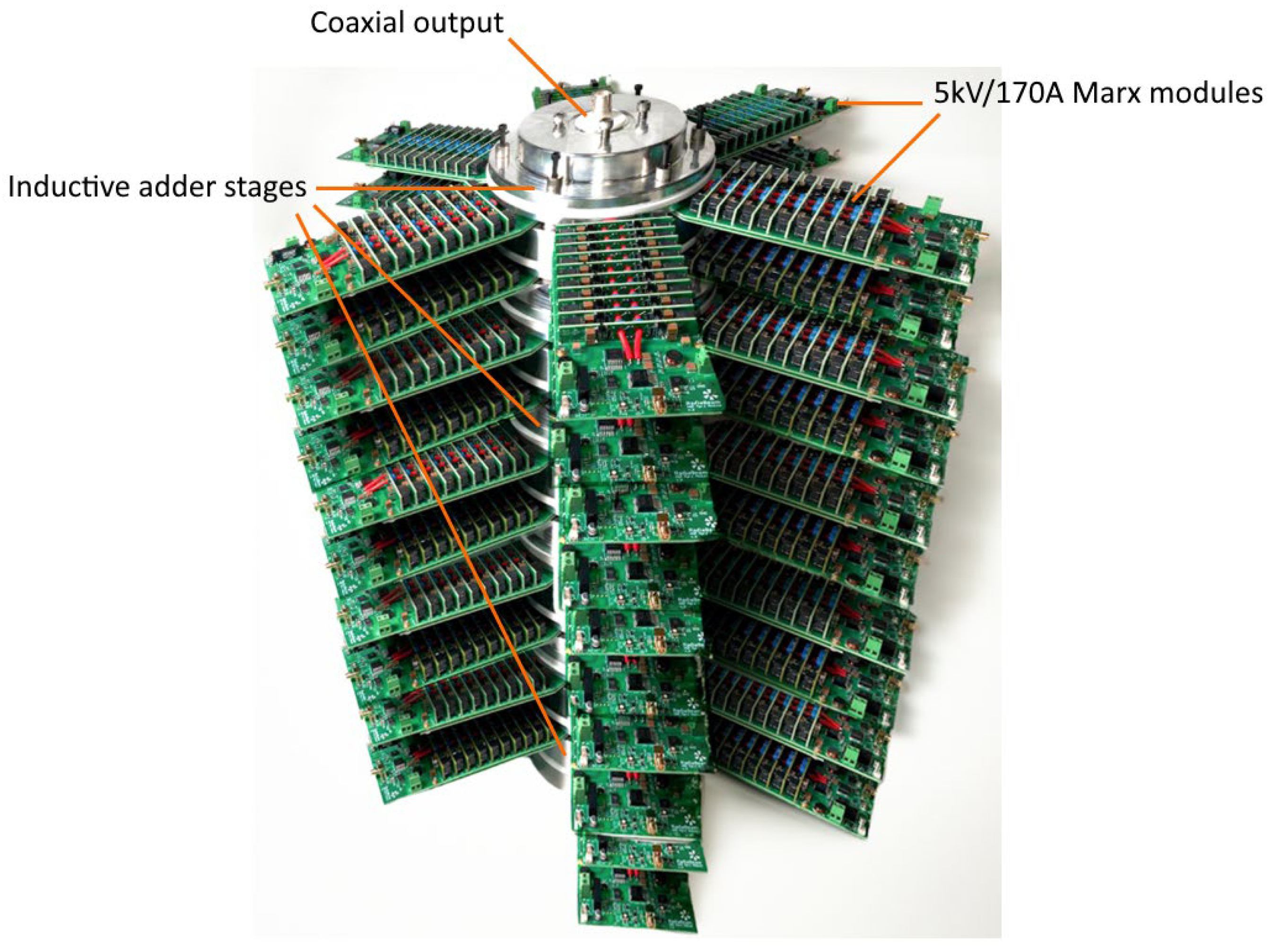
To address these challenges and meet the demands for a commercial solution for the EIC kicker drivers, RadiaBeam has developed a pulse generator based on a distributed pulser topology [
11], utilizing modern GaN transistors as switching devices. GaN is an emerging technology that supports both high peak and average power operation, while offering extremely short switching times on the nanosecond scale. This capability provides additional margin for the stringent rise and fall time requirements of the EIC kickers. The novelty of our approach lies in combining a Marx topology [
12] with an inductive adder, as illustrated in
Figure 1.
2. System Architecture Development
The development of the pulser is being carried out in sequential stages. First, a single GaN chip was individually tested to validate its optimal current rise time [
13]. A specialized board was built and tested to drive a single transistor at 500 V (80% of the maximum allowed) with a low-impedance load (7.5–10 Ω, to draw maximum current) and a pulse duration of 40 ns (nominal requirement of the EIC). The circuit design included a precise pulse-forming network, supply line stabilizers, and a dedicated two-stage transistor driver. The output stage was configured in a push–pull topology. Testing demonstrated that with proper management of parasitic parameters and enhanced stability of the driver and supply circuits, the transistor could achieve a commutation rate of
di/dt = 12.5 A/ns, meeting the EIC’s stringent short pulse edge requirements.
In the second stage, the transistors were arranged into Marx modules, followed by the iterative optimization of the series and parallel configurations of the switching elements and their driver circuits. The goal was to achieve outputs of several kilovolts and hundreds of amperes per module, keeping the total number of modules under 100. A detailed study of the pulser topology was conducted, leading to an optimal combination of parallel switching sub-elements. This resulted in each module achieving a 5 kV/170 A output. An additional analysis ensured a balanced design by considering factors such as the number of sub-elements, individual power levels, system complexity, footprint, thermal management, and overall cost.
Finally, the Marx modules were integrated into a single output channel, and the module count was scaled to achieve a total combined pulsed output of 25 kV and 300 A, with the ultimate goal of scaling to 50 kV and 1 kA.
2.1. Marx Module
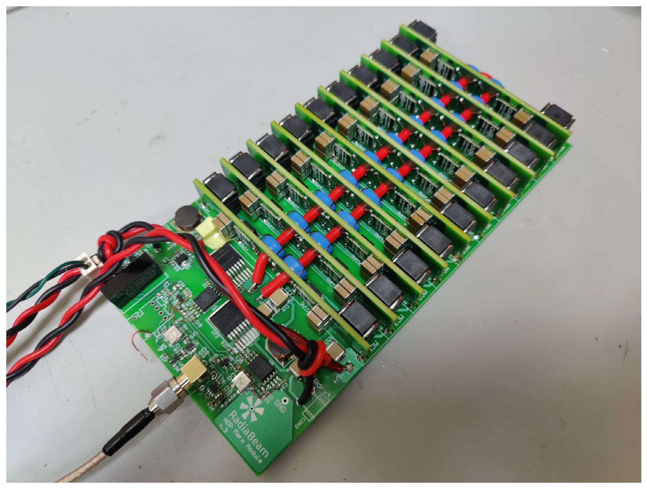
The Marx modules have been designed to enhance the output pulse parameters while simplifying the assembly process and improving compactness. Each module consists of a combiner board that integrates 10 cell boards (or Marx cells, see
Figure 2). The combiner board incorporates cell drivers, a pulse-shaping circuit, and power supply circuits for the storage capacitors of the cells. Synchronization pulses can be delivered via both coaxial and optical inputs.
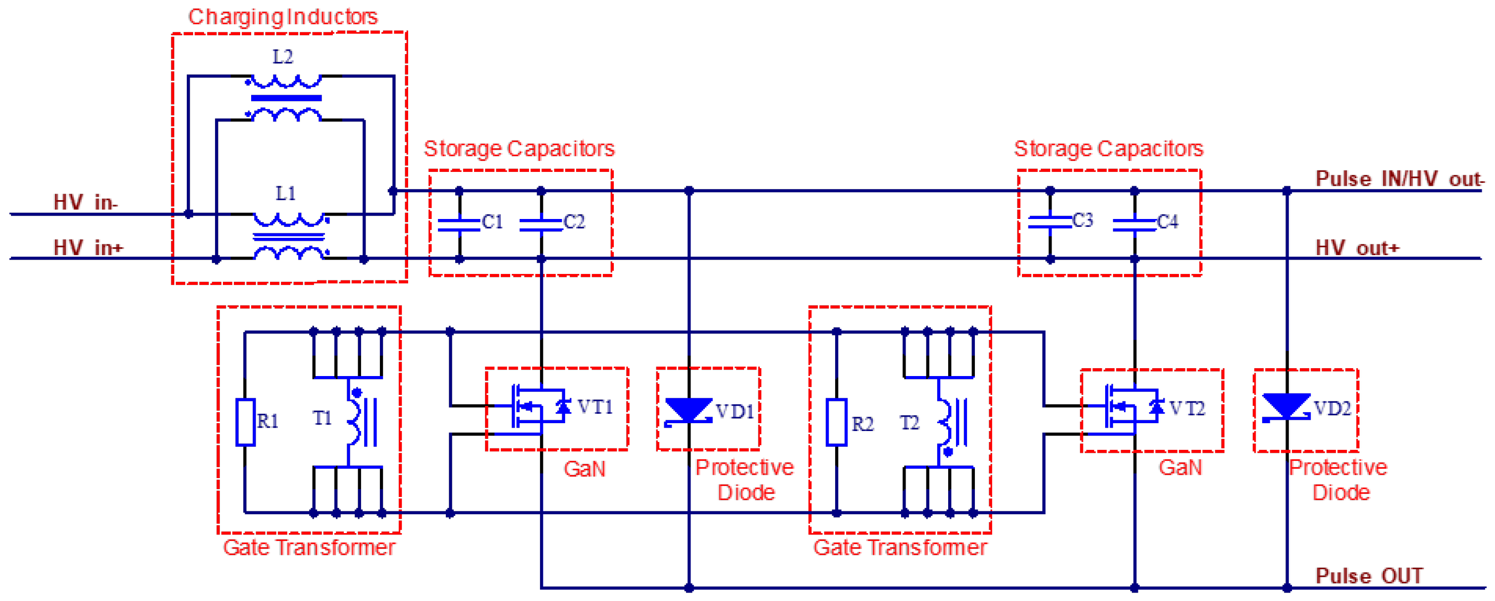
The transistor driver utilizes a push–pull design configured as a half-bridge circuit [
14]. This configuration enables the generation of bipolar current pulses to control the transistor gates, improving the falling edge of the high-voltage pulse and facilitating the re-magnetization of the core.
Each cell contains two GaN transistors connected in parallel, each with its own control transformer, storage capacitors, protective diodes, and charging chokes. Common-mode chokes are used to provide low inductance for the charging current while offering high inductance when the transistors are off, effectively isolating each cell during the switching process. Protective diodes are included to prevent transistor breakdown caused by voltage drops across the storage capacitors. Each cell incorporates four storage capacitors—two for each transistor—to minimize the length of the power circuit and reduce parasitic effects.
The cells are assembled on individual printed circuit boards with double-sided mounting to improve compactness (see
Figure 3). The module design minimizes the length of the transistor gate drive paths, reducing parasitic effects. The gates are controlled using current transformers, with the cores and four secondary windings placed in close proximity to the gates. This arrangement ensures low transformer leakage inductance, resulting in sharper pulse edges. Both transformers are connected in parallel, but their secondary windings are cross-connected, with the primary winding currents flowing in opposite directions. This configuration enhances the balance between the drives of the two parallel transistors, improving overall performance.
2.2. Power Combiner
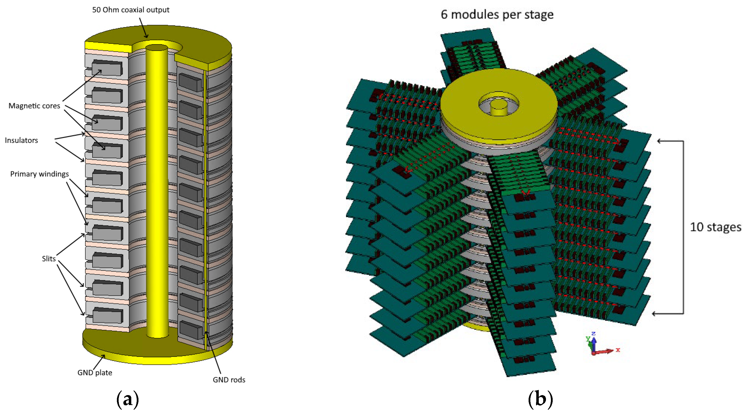
An inductive adder was chosen as the most practical approach to combine power from several Marx modules. It allows the adding of currents and voltages from several modules and matching them with a load [
15]. This method offers the most axially symmetric and compact configuration for connecting the modules to a common load. The inductive adder acts as a single-turn transformer, with its center conductor serving as the secondary winding and forming a coaxial line.
To generate pulses with an amplitude of 50 kV/1 kA using the developed 5 kV/170 A modules, an inductive adder with 10 transformers connected in series is required. Each transformer must combine the output of six modules in parallel, resulting in a total of 60 modules.
We have designed an inductive adder specifically for this application. The nanocrystalline was selected as a magnetic core material, which has high permeability up to 70 × 10
3 and a saturation induction of 1.23 T. This material can operate with a maximum change in magnetic induction of 0.5 T without core reset. The design process began with basic calculations [
16], starting with determining the required cross-sectional area of the magnetic core by calculating the change in magnetic induction during the pulse duration of 40 ns and voltage amplitude of 5 kV:
where
Vp is the voltage amplitude in the pulse,
tp is the pulse duration,
Nt is the number of primary winding turns, and
Ae is the cross-section area of the magnetic core. The value of
Ae in our case should be more than 4 cm
2, which corresponds to 0.5 T of magnetic induction in order to work in the linear region of the hysteresis loop without magnetic core saturation.
Next, the geometry of the toroidal core (outer diameter, inner diameter, and height) must be determined based on output impedance of inductive adder. The output impedance of the inductive adder is determined by the ratio of the internal and external conductor and height of the cell. The outer conductor radius will be determined by the inner diameter of the magnetic core and the thickness of the primary winding wall. The diameter of the central rod is determined with the diameter of the outer conductor via estimation of the combiner cell capacitance calculated as follows:
where
εr is the relative permittivity of the insulator between the inner and outer conductors,
l0 is the height of the cell,
ro is the radius of the outer conductor, and
ri is the radius of the central rod of the secondary winding. The inductance of the cell is calculated as follows:
where µ
r is the relative magnetic permeability of the insulator between the inner and outer conductors. Thus, the cell impedance is determined by the formula:
where
La is the additional inductance of the input circuits of the module of 3.5 nH. By varying geometric dimensions, the output impedance of 52 Ohm was obtained with the following dimensions:
ro = 80 mm,
ri = 40 mm, and
l0 = 45 mm. All the aforementioned calculations provided the initial dimensions for the inductive adder. The next step involved creating a full 3D electromagnetic (EM) model of the adder and running detailed simulations using CST Microwave Studio 2024 [
17]. The 3D models of the inductive adder and the 50 kV channel assembly are shown in
Figure 4.
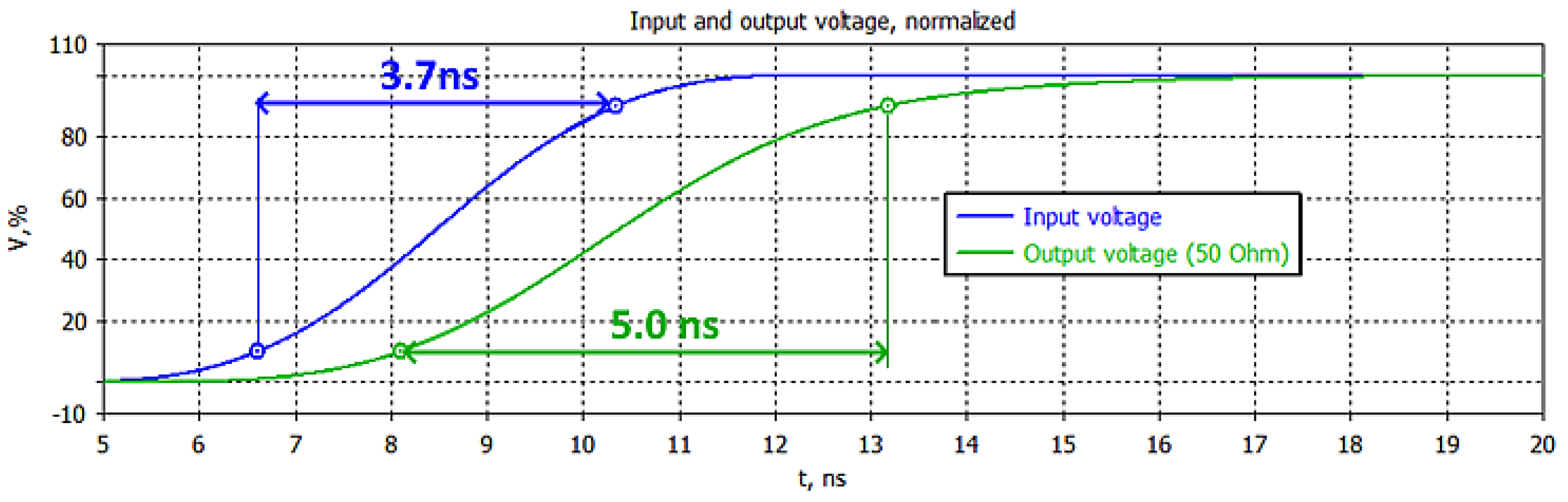
Transient simulations were conducted using 60 ideal voltage sources, each representing the output of a single Marx module (5 kV peak voltage). The simulated input and combined output waveforms are presented in
Figure 5. The input waveforms were characterized by the following parameters: ~4 ns rise and fall times (10–90%) and a 30 ns flat-top duration (90%). These parameters align with the experimentally obtained signals from the fabricated modules, as reported in the following sections.
The simulated waveforms indicate that the inductive adder preserves the pulse shape, with only a slight stretching of the rise and fall edges by approximately 1.5 ns.
3. High-Power Testing Results
We fabricated a prototype of the inductive adder, beginning with two stages, and successfully tested it with four Marx modules, achieving a total combined output of 10 kV/340 A. Following the successful high-power testing of the 2S2P configuration, we sequentially increased the number of modules and added additional stages to the inductive adder, culminating in the current 6S2P configuration with a 25 kV/300 A output. These results validate the feasibility of our approach and demonstrate the potential for scaling to the target output of 50 kV/1 kA.
3.1. Marx Modules
A 10-cell Marx module, shown in
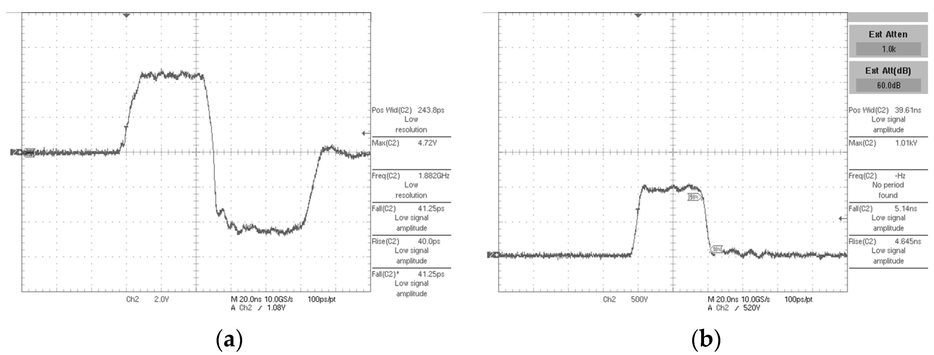
Figure 3, was assembled and tested at a maximum input voltage of 500 V. The tests were conducted using a 30 Ω resistive load, assembled from a combination of resistors to ensure low parasitic inductance, the required operating voltage, and the ability to dissipate high pulsed power. Initially, the driver was configured for synchronous control of all transistors in the cells. The rise and fall edges of the bipolar control pulse (
Figure 6a) were below 10 ns, enabling sufficiently fast opening and closing of the transistors.
After validating the driver’s performance, voltage was applied to the module’s input, starting at 100 V and gradually increasing while monitoring the output signal. The oscillogram of the output voltage pulse at 100 V input is shown in
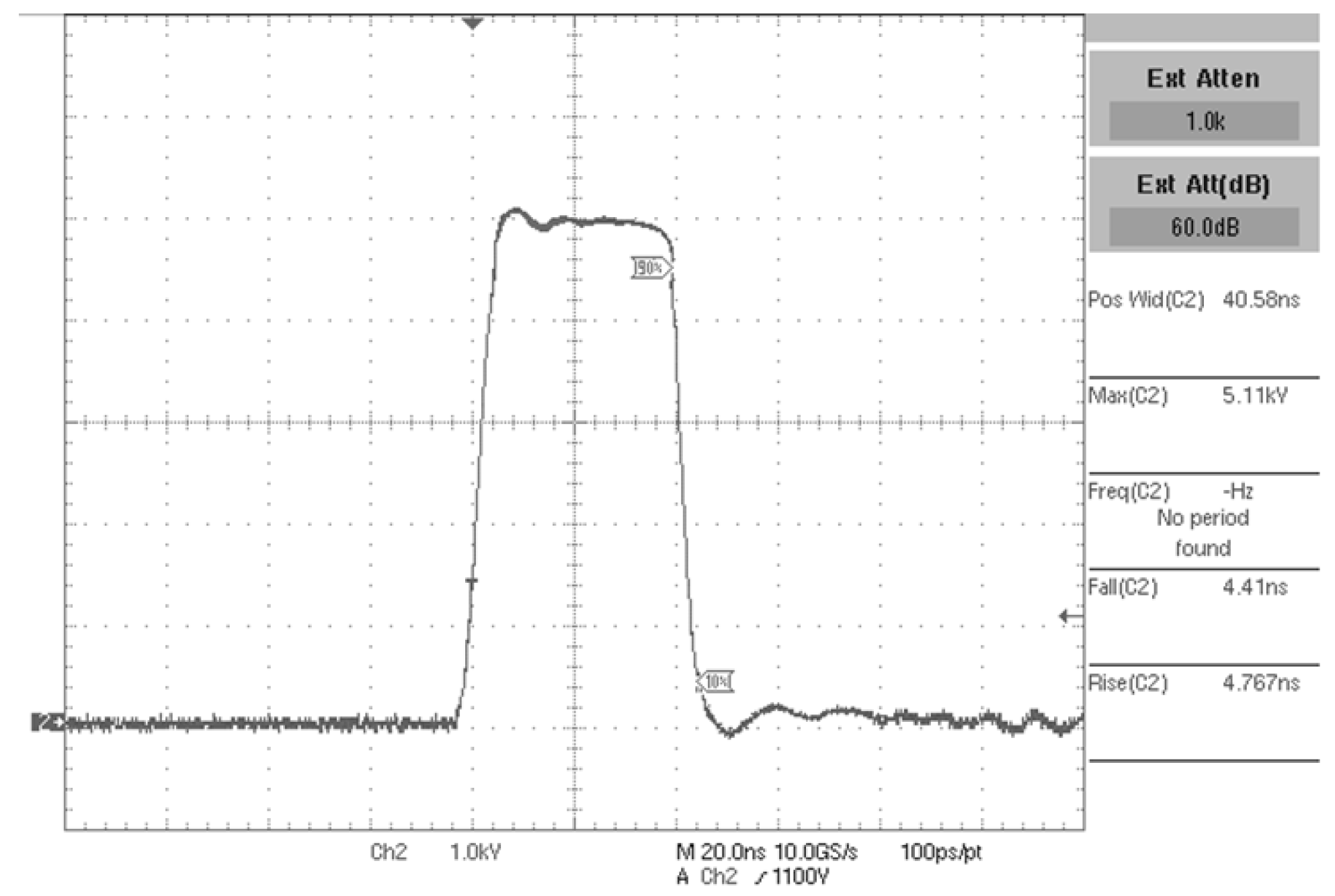
Figure 6b. At the maximum input voltage of 500 V, the module achieved the target 5 kV output, as shown in
Figure 7. The module demonstrated rise and fall times of less than 5 ns and a flat-top duration of approximately 30 ns.
3.2. High-Power Testing with an Inductive Adder
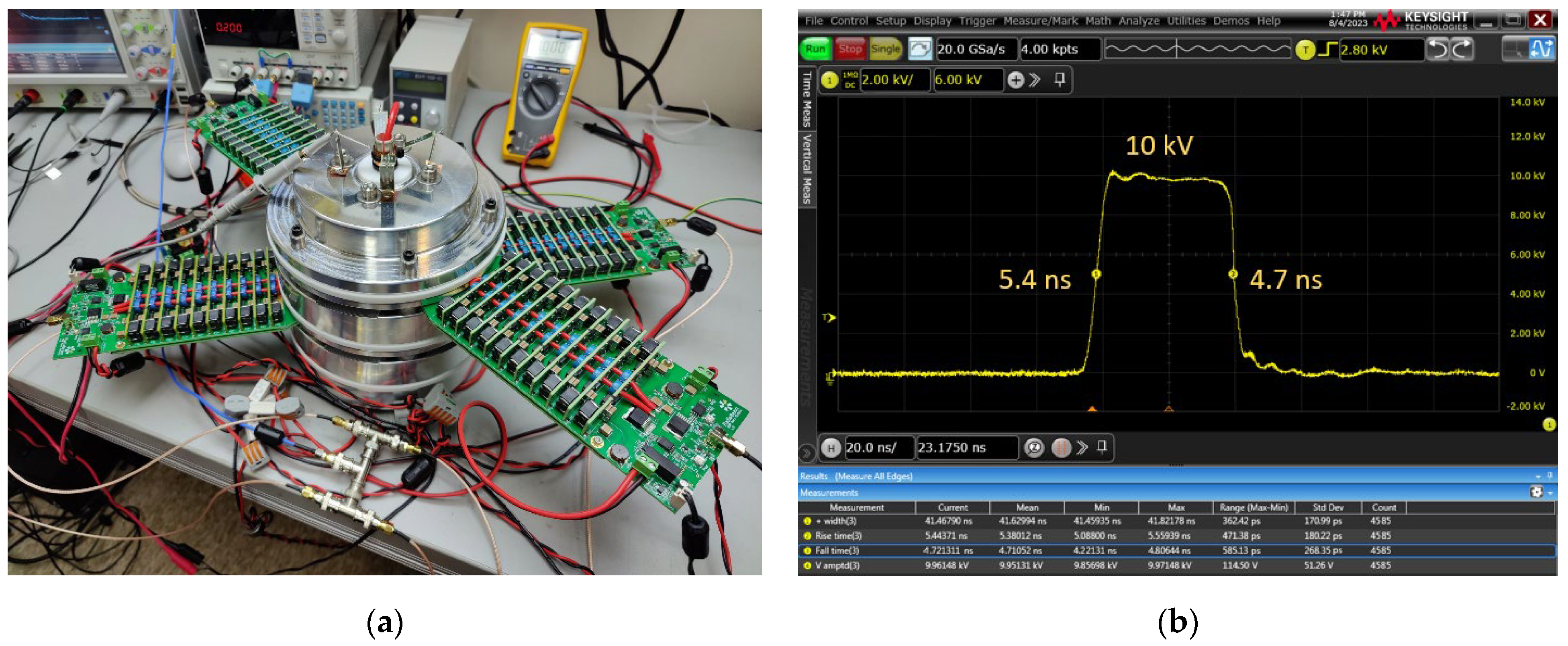
All components of the inductive adder were fabricated in the RadiaBeam machine shop and subsequently assembled. Initial testing was conducted with a two-stage configuration, each stage containing two modules (2S2P configuration). The four Marx modules were connected to the inductive adder, a high-voltage power supply, and a separate power supply for the control and driver circuits. The synchronization signal was delivered via coaxial splitters.
The magnetic core reset winding—a high-voltage insulated wire passing through the central conductor of the inductive adder’s coaxial output—was powered by a dedicated DC source. A choke was used to isolate this power source from high-voltage pulses. The fully assembled test stand is shown in
Figure 8a.
During testing, output pulse oscillograms were obtained from the inductive adder for various input DC voltages (
Figure 8b). The oscillograms confirm the successful operation of the inductive adder with the Marx modules, as evidenced by the observed output voltage doubling. The rise and fall times meet the EIC requirements, measuring 5.4 ns and 4.7 ns, respectively.
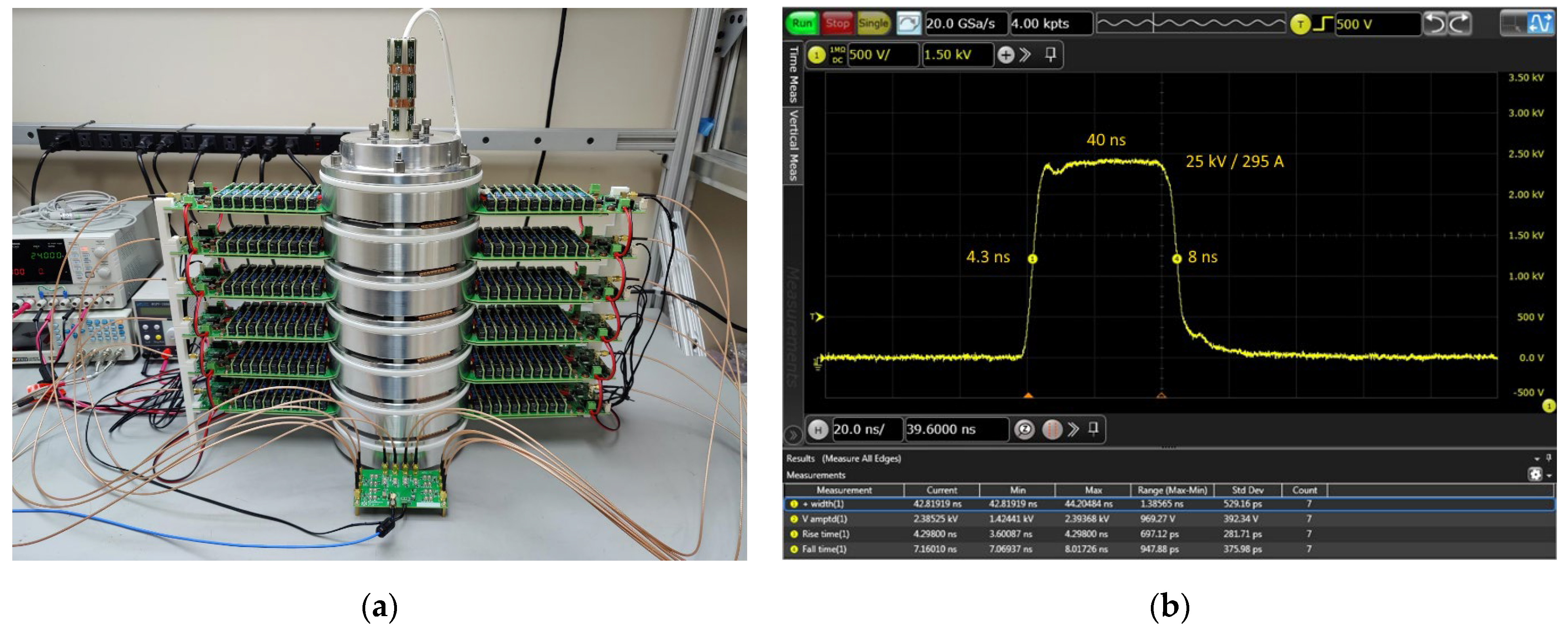
The primary objective of the next experiment was to generate pulses with an amplitude of up to 25 kV. To achieve this, six stages of an inductive adder and 12 Marx modules were designed and assembled in a 6S2P configuration (
Figure 9a). Each module delivers a pulse current of up to 150 A, allowing the inductive adder to achieve a total output current of 300 A (with two modules per stage).
The equivalent resistive load for the inductive adder, based on the selected topology, was calculated to be 83.3 Ω. For the experiment, a load of 85 Ω was selected. Initial tests revealed instability in the module operation, observed as oscillations during pulse turn-off. Further investigation indicated that these oscillations were influenced by the amplitude of the voltage and current, as well as the pulse repetition frequency (
Figure 9b).
4. Discussion
RadiaBeam has developed and tested a high-output pulse generator based on a distributed pulser topology, utilizing advanced GaN transistors as switching devices in a Marx architecture combined with an inductive adder for pulse combination. This innovative design supports both high peak and average power operation while achieving nanosecond-scale switching times, ensuring it meets the stringent rise and fall time requirements of the EIC kickers.
After successfully testing 12 modules in a 6S2P configuration, the next step involves assembling 24 modules in a 6S4P configuration. This setup will enable the inductive adder to deliver up to 500 A to the required 50 Ω load impedance. Ultimately, the goal is to assemble 60 modules in a 10S6P topology to achieve a pulsed output of 50 kV/1 kA.
5. Conclusions
The developed inductive adder presents opportunities for further optimization. The fabricated prototype introduced approximately 1 ns of additional rise and fall time to the modules, likely due to parasitic effects. These effects can be mitigated through refined 3D electromagnetic simulations and the implementation of impedance-matched geometries [
19].
One potential improvement involves reducing the number of series Marx cells per module from the current 10S configuration to 8S. This adjustment would decrease the stage voltage, thereby lowering the thickness of the intra-stage isolation. Consequently, this reduction would minimize parasitic inductance, leading to enhanced system performance.
Post-pulse oscillations have, in some instances, caused transistor breakdowns within one of the module cells. To address this, snubber circuits were added to each individual transistor, effectively reducing the amplitude of the oscillations and protecting the transistors from damage. However, this solution increased the fall time of the pulse, lengthening its duration (~8 ns achieved at 25 kV operation per
Figure 9). In comparison, a FID-based solution demonstrated 20 ns at 50 kV operation [
20]. To eliminate oscillations while maintaining an acceptable pulse fall time, it is critical to reduce parasitic inductance and optimize transistor control. Stability issues will be resolved by focusing on the topology of the Marx module. Specifically, minimizing the length of the power circuit within the module cells, while preserving the gate drive pulse characteristics, will prevent the degradation of output pulse rise and fall times. The modified module will undergo testing across a range of loads, including those exceeding the nominal current rating, to validate its performance and stability.
Beyond module upgrades, further optimization will target the material and dimensions of the magnetic cores in the inductive combiner and the geometry of the primary windings. Key objectives include reducing the loop area of the primary winding, enhancing the coupling coefficient of the transformers, and lowering the height of both individual stages and the overall combiner structure. These enhancements aim to improve performance while reducing the system’s size and weight.
Author Contributions
Conceptualization, A.S. and E.I.; software, E.I.; validation, E.I. and A.P.; investigation, A.S.; writing—original draft preparation, A.S., E.I. and S.K.; supervision, S.K.; project administration, A.S. All authors have read and agreed to the published version of the manuscript.
Funding
This work supported by the U.S. Department of Energy, Office of Nuclear Physics under SBIR grant DE-SC0021548.
Data Availability Statement
Data are available from the authors upon reasonable request.
Conflicts of Interest
All authors were employed by RadiaBeam Technologies, LLC. All authors declare that the research was conducted in the absence of any commercial or financial relationships that could be construed as a potential conflict of interest.
References
- Accardi, A.; Albacete, J.L.; Anselmino, M.; Armesto, N.; Aschenauer, E.C.; Bacchetta, A.; Boer, D.; Brooks, W.K.; Burton, T.; Chang, N.-B.; et al. Electron-Ion Collider: The next QCD Frontier. Eur. Phys. J. A 2016, 52, 1–100. [Google Scholar] [CrossRef]
- Khalek, R.A.; D’Alesio, U.; Arratia, M.; Bacchetta, A.; Battaglieri, M.; Begel, M.; Boglione, M.; Boughezal, R.; Boussarie, R.; Bozzi, G.; et al. Snowmass 2021 White Paper: Electron Ion Collider for High Energy Physics. arXiv 2022, arXiv:2203.13199. [Google Scholar]
- Bhat, P.C.; Jindariani, S.; Ambrosio, G.; Apollinari, G.; Belomestnykh, S.; Bross, A.; Butler, J.; Canepa, A.; Dasu, S.; Elvira, D.; et al. Future High Energy Colliders and Options for the U.S. J. Instrum. 2023, 18, P12007. [Google Scholar] [CrossRef]
- Shiltsev, V.; Zimmermann, F. Modern and Future Colliders. Rev. Mod. Phys. 2021, 93, 015006. [Google Scholar] [CrossRef]
- Sangroula, M.; Liaw, C.; Liu, C.; Sandberg, J.; Tsoupas, N.; Xiao, B.; Sun, X. Design Update on the HSR Injection Kicker for the EIC. In Proceedings of the 13th International Particle Accelerator Conference (IPAC’22), Bangkok, Thailand, 12–17 June 2022; pp. 1904–1907. [Google Scholar]
- Judd, E.G.; Bland, L.C.; Crawford, H.J.; Engelage, J.; Landgraf, J.M.; Llope, W.J.; Nelson, J.M.; Ng, M.; Ogawa, A.; Perkins, C.; et al. The Evolution of the STAR Trigger System. Nucl. Instrum. Methods Phys. Res. A 2018, 902, 228–237. [Google Scholar] [CrossRef]
- Larsson, A. Gas-Discharge Closing Switches and Their Time Jitter. IEEE Trans. Plasma Sci. 2012, 40, 2431–2442. [Google Scholar] [CrossRef]
- Grishanov, B.I.; Podgorny, F.V.; Rümmler, J.; Shiltsev, V.D. Very Fast Kicker with High Repetition Rate for Accelerator Applications. Nucl. Instrum. Methods Phys. Res. A 1997, 396, 28–34. [Google Scholar] [CrossRef]
- Zhang, W.; Fischer, W.; Hahn, H.; Liaw, C.J.; Sandberg, J.; Tuozzolo, J. Accelerator Fast Kicker R&D with Ultra Compact 50MVA Nano-Second FID Pulse Generator. In Proceedings of the 19th IEEE Pulsed Power Conference, San Francisco, CA, USA, 16–21 June 2013. [Google Scholar] [CrossRef]
- Butler, N.; Niell, F.; Gaudreau, M.; Kempkes, M.; Munderville, M. Solid-State Pulsed Power System for a Stripline Kicker. In Proceedings of the 28th Linear Accelerator Conference LINAC’16, East Lansing, MI, USA, 25–30 September 2016; pp. 824–826. [Google Scholar]
- Smirnov, A.Y.; Agustsson, R.; Benson, S.V.; Gavryushkin, D.; Guo, J.; Kutsaev, S.V.; Moro, A.; Park, G.T.; Smirnov, A.V.; Wang, H.; et al. Ultrafast High-Voltage Kicker System for Ion-Clearing Gaps. Photonics 2021, 8, 507. [Google Scholar] [CrossRef]
- Ivanov, E.; Kutsaev, S.V.; Pronikov, A.; Smirnov, A.Y. Ultralightweight Power System for Human-Portable Linac-Based X-Ray Sources. IEEE Trans. Nucl. Sci. 2023, 70, 2158–2164. [Google Scholar] [CrossRef]
- Smirnov, A.Y.; Agustsson, R.; Ivanov, E.; Kutsaev, S.V. A 50 KV Pulse Generator for Fast Kickers. In Proceedings of the 15th International Particle Accelerator Conference (IPAC24), Nashville, TN, USA, 19–24 May 2024; pp. 3806–3808. [Google Scholar]
- Zhang, Z.; Thomsen, O.C. Optimal Design of a Push-Pull-Forward Half-Bridge (PPFHB) Bidirectional DC–DC Converter with Variable Input Voltage. IEEE Trans. Ind. Electron. 2012, 59, 2761–2771. [Google Scholar] [CrossRef]
- Hartmann, W.; Fleck, R.; Hergt, M. Concept of an Inductive Voltage Adder for Industrial Applications. In Proceedings of the 19th IEEE Pulsed Power Conference, San Francisco, CA, USA, 16–21 June 2013. [Google Scholar] [CrossRef]
- Zhang, W.; Eng, W.; Pai, C.; Sandberg, J.; Tan, Y.; Tian, Y. A Simplified Approach to Analyze and Model Inductive Voltage Adder. In Proceedings of the PAC07, Albuquerque, NM, USA, 25–29 June 2007. [Google Scholar]
- CST Studio Suite. Available online: https://www.3ds.com/products/simulia/cst-studio-suite (accessed on 10 November 2024).
- Magnetic Materials. Available online: https://www.metglas.com/magnetic-materials/ (accessed on 10 November 2024).
- Huiskamp, T.; Van Oorschot, J.J. Fast Pulsed Power Generation with a Solid-State Impedance-Matched Marx Generator: Concept, Design, and First Implementation. IEEE Trans. Plasma Sci. 2019, 47, 4350–4360. [Google Scholar] [CrossRef]
- Zhang, W.; Blaskiewicz, M.; Hershcovitch, A.; Liaw, C.J.; Lovelace, H., III; Mapes, M.; McIntyre, G.T.; Mi, J.-L.; Montag, C.; Pai, C.; et al. Pulsed Systems for eRHIC Beam Injection and Extraction. In Proceedings of the IPAC-18, Vancouver, BC, Canada, 2 May 2018. [Google Scholar] [CrossRef]
| Disclaimer/Publisher’s Note: The statements, opinions and data contained in all publications are solely those of the individual author(s) and contributor(s) and not of MDPI and/or the editor(s). MDPI and/or the editor(s) disclaim responsibility for any injury to people or property resulting from any ideas, methods, instructions or products referred to in the content. |
© 2025 by the authors. Licensee MDPI, Basel, Switzerland. This article is an open access article distributed under the terms and conditions of the Creative Commons Attribution (CC BY) license (https://creativecommons.org/licenses/by/4.0/).


