1. Introduction
The quantum confinement effect of multi-quantum-well (MQW) light-emitting diodes (LEDs) is used to achieve highly efficient light emission and fast response speed [
1]. In recent years, the application of LEDs in visible-light communication (VLC) [
2] and display backlights [
3] has gained significant attention. As the core light-emission devices of VLC or display systems, LEDs need a wide bandwidth and high response speed in VLC modulation and PWM (Pulse-Width Modulation) display backlight dimming.
The characteristics of MQW LEDs, such as recombination rate and luminous efficiency, are influenced by carrier recombination within the quantum wells. In particular, the carrier lifetime, jointly determined by radiative recombination, Auger recombination, and surface recombination, plays a pivotal role in the spontaneous emission rate, carrier distribution, high-frequency response, and other aspects of LED device performance.
In related research, numerous studies have explored the impacts of factors such as the quantum well period, device size, material defects, buffer layer materials, and temperature on device performance [
4,
5,
6,
7,
8,
9,
10]. However, these factors invariably manifest as the generation and recombination of carriers within the device (i.e., carrier lifetime). Therefore, the work presented in this paper simplifies the variables by focusing on three recombination mechanisms of carriers within the device. Based on this, a more detailed carrier transport model is established to better characterize the carrier distribution in various regions of the MQW LEDs.
In this work, we fabricated an AlGaInP/GaInP MQWs LED sample and built its carrier continuity equation model. With the AC small-signal analysis, the MQW capacitance at forward bias voltages was calculated. We checked the carrier distribution across different quantum well regions, and we assessed the impact of carriers’ recombination mechanisms on negative capacitance.
2. Experiments
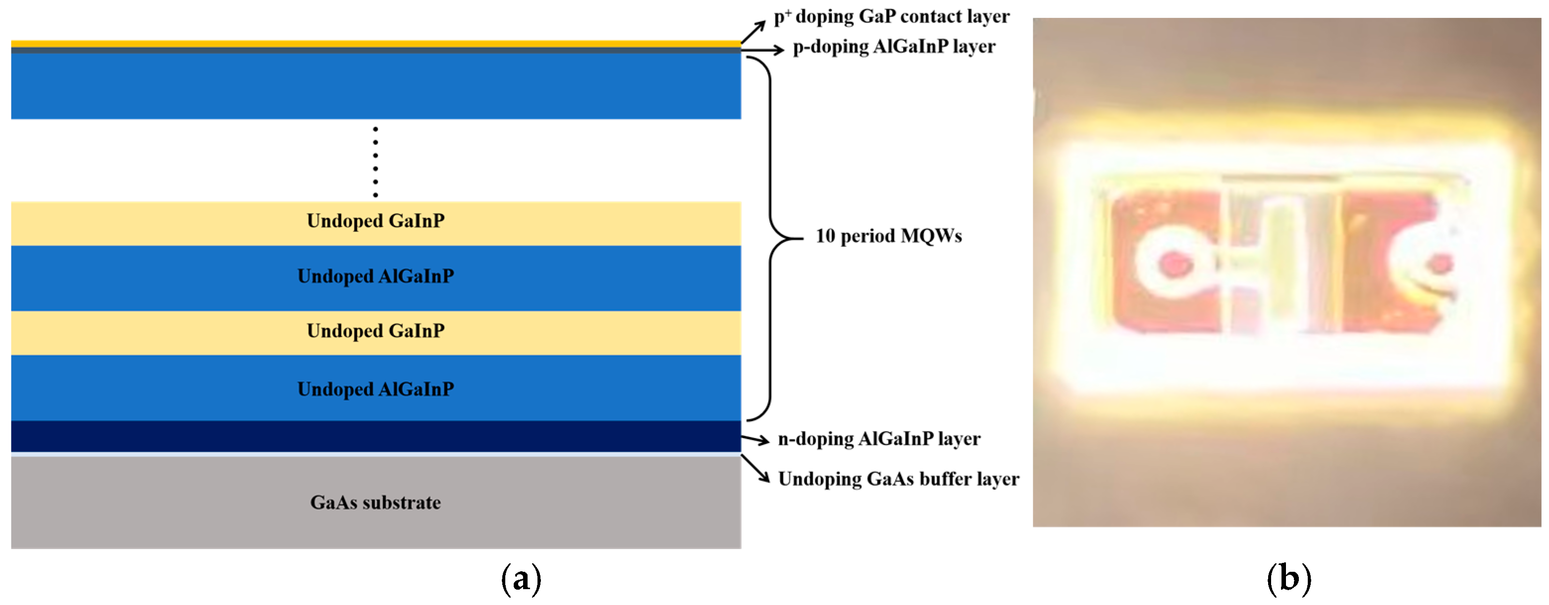
An AlGaInP/GaInP MQW LED was fabricated to research the NC phenomenon. The MQW LED material was grown on a GaAs substrate by Metal–Organic Chemical Vapor Deposition (MOCVD) technology. The source materials were trimethylindium (TMI), trimethylgallium (TMG), methylaluminium (TMA), PH
3, and AsH
3. Dimethylzinc (DMZ) served as the doping source for the p-type layer, while biscyclopentadienylmagnesium (Cp
2Mg) and SiH
4 served as the doping sources for the n-type layer. The growth temperature was 650~680 °C and the total pressure was 9.3 × 10
3 Pa. The V/III ratio was ~550, and the growth rate was ~2 µm/h. The LED’s layers, from bottom to top, were as follows: a 0.3 μm undoped GaAs buffer layer, a 3 μm 2 × 10
18 cm
−3 n-doped AlGaInP layer, 10-period undoped AlGaInP (6 nm)/GaInP (4 nm) MQWs, a 0.4 μm 4 × 10
17 cm
−3 p-doped AlGaInP layer, and a 0.1 μm 1 × 10
20 cm
−3 p
+-doped GaP contact layer. The epitaxial growth schematic of the MQW LED is shown in
Figure 1a. In order to achieve better light output, the grown epitaxy layers were transferred onto a transparent sapphire substrate by the wafer bonding process, and the LED mesa size was set as 90 μm × 150 μm.
After LED mesa and N-layer ICP etching, a 600 nm SiO
2 passivation layer was used to cover the P and N layers. For electrical contacts, a 200 nm thick Au/Ge/Ni alloy layer was deposited as the N-type electrode through electron beam evaporation, paralleled by a similarly dimensioned Au/Zn alloy layer serving as the P-type electrode. For the convenience of C-V testing, the P-pad and N-pad were evaporated on the surface of the P and N electrodes to achieve the connection between the chip and substrate. The microscope photo of this MQW LED is shown in
Figure 1b.
Then, the LED chip was assembled on a test PCB circuit through flip-chip soldering. The capacitance–voltage (C-V) characteristics of the MQW LED were measured by a Keithley 4200A parameter analyzer connected to a probe station.
3. Theoretical Analysis
Based on the above LED device structure, we built a calculation model to research the MQW LED’s carrier distribution and capacitance characteristics. First, we used the carrier continuity equation and MQW boundary conditions to calculate the carrier concentration and total junction current. Then, the LED junction capacitance was verified with the AC small-signal analysis.
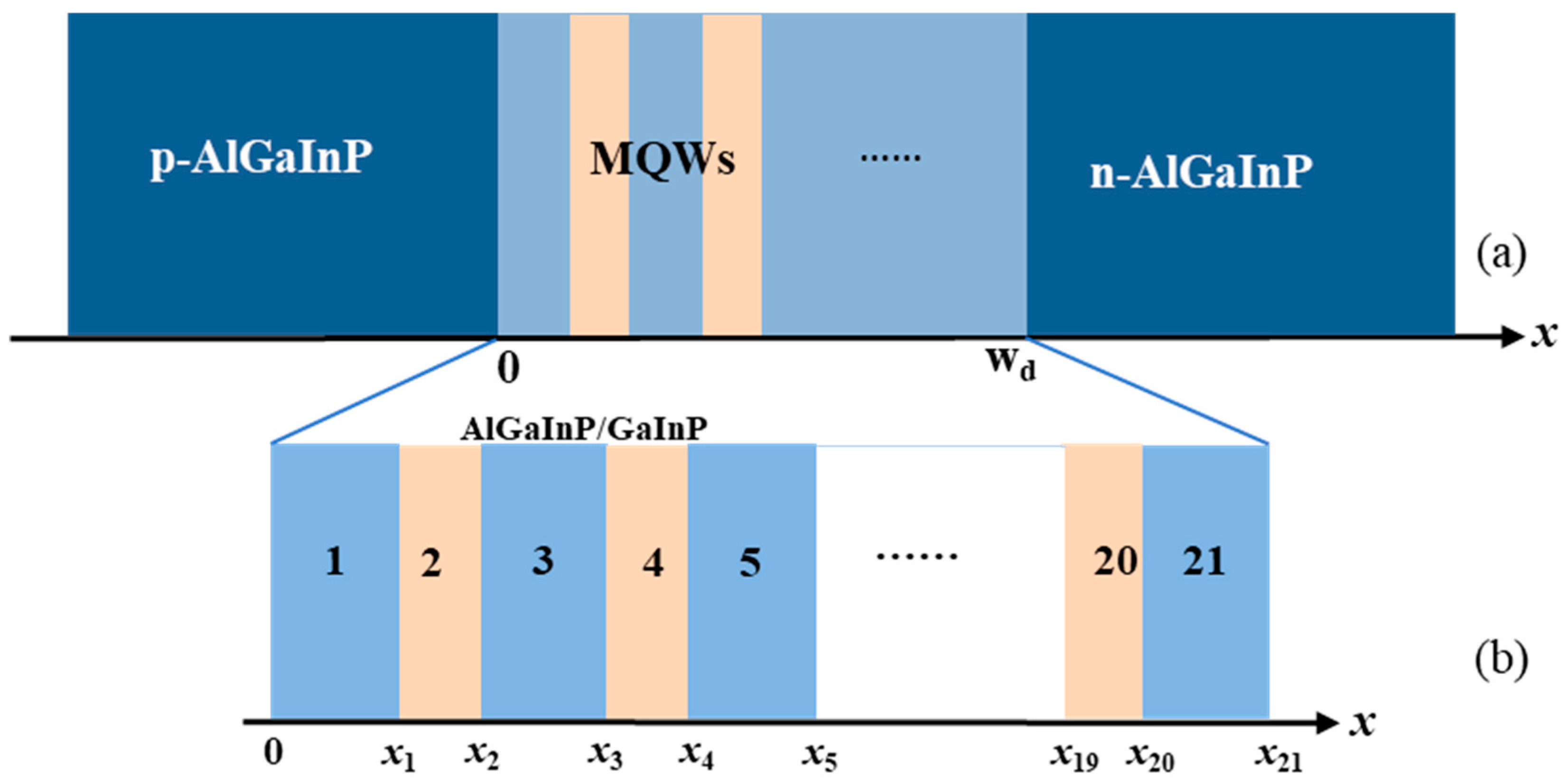
The MQW LED model’s structure is shown in
Figure 2, including P, N, and AlGaInP doping layers and AlGaInP/GaInP MQWs. The 10-period MQWs are composed of 11 AlGaInP barrier layers sandwiched with 10 GaInP well layers. The left boundary of the MQWs is set as the
x-axis 0 point, and the width of the MQWs is
;
x1~
x21 represent the boundary position of every AlGaInP/GaInP layer, and the MQWs’ last AlGaInP boundary
.
The steady-state continuous equations of electrons in the P-doped region and the MQWs are shown in Equations (1) and (2), respectively [
11]:
In the LED’s P-doped region, the diffusion of non-equilibrium minority carrier electrons satisfies Equation (1), where is the electron concentration, is the electron diffusion coefficient in the P-doped region, and is the common lifetime of electrons. In different regions of the MQWs, there are electric fields (i = 1, 2⋯21) caused by bias voltage, and the electrons and holes in the MQWs exhibit diffusion, drift, and recombination. In Equation (2), and are the MQWs’ material electron diffusion coefficient and electron mobility, respectively, and represents the different recombination lifetimes of the MQWs’ 21 layers.
The analysis of holes’ concentration is similar to that for electrons; holes are injected from the P-doped region, and the steady-state continuity equations of holes in the corresponding N-doped region and MQW region are shown in Equations (3) and (4), respectively:
where
is the hole concentration, while
and
are the hole diffusion coefficient and lifetime in the N-doped region, respectively. The
(
i = 1, 2⋯21) are the hole diffusion coefficient, mobility, and recombination lifetime of the MQW layers, respectively.
To solve the second-order linear differential equations with constant coefficients as shown in Equations (1)–(4), given that the equations have one positive and one negative characteristic root, and considering the diffusion of carrier concentration along the positive direction of the
x-axis [
12], we selected the general solution containing the positive characteristic root as the practical solution for the carrier concentration of these equations.
The carrier recombination lifetime
in Equations (1)–(4) is shown in Equation (5), combining the spontaneous radiation lifetime (
), non-equilibrium carrier indirect recombination lifetime (
), and Auger recombination lifetime (
) [
11].
Under forward voltage bias, electrons are injected from the highly doped N region into the undoped quantum well region. Based on the large carrier injection [
11], we set the electron intensity at the N region and MQW boundary (
as follows:
where
is the intrinsic electron concentration of AlGaInP, and
is an injection factor.
The electrons in the MQWs are driven by bias voltage
and built-in potential caused by the quantum well conduction band difference
. We set the electron intensity
(
i = 1, 2⋯20) at the boundary of each region in the MQWs as shown in Equation (7):
Then, the electrons diffuse into the P-type doping region through the MQWs, and the boundary conditions for
are given by Equation (8):
For the holes injected from the highly doped P region into the MQWs, the boundary conditions at the interface between the P region and the MQWs are closely related to the electrons’ behavior and distribution in the adjacent regions. The built-in potential of the MQWs is caused by the quantum well valence band difference . With the carrier lifetime and boundary conditions described by Equations (5)–(8), we can determine the carrier concentrations by the solution of Equations (1)–(4).
Then, the LED total junction current
can be derived by the carrier concentration at the boundary of the PN region (
and
) and MQWs.
where
is the diffusion region current of the
n and
p regions, and
is the sum of the carrier recombination currents within the MQWs.
where
A is the area of the active region, while
a and
b represent the upper and lower boundaries of each region, respectively.
Under the AC working condition, the DC bias voltage
is mixed with AC small signals (
and the input voltage in Equation (6) changes to
. The total current
in Equation (9) has a similar AC form, i.e.,
, where
and
are the DC and AC amplitude, respectively. The calculation parameters in this work include an AlGaInP barrier layer width of 6 nm, GaInP well layer width of 4 nm, total quantum well width
of 106 nm, device area
A of 1.35 × 10
−8 m
2, AC small-signal frequency
of 1 kHz, AC voltage
of 10 mV, and injection factor
of 1.5; the other material parameters of AlGaInP and GaInP were chosen from reference [
13], and the main parameters used in the model are shown in
Table 1.
4. Results and Discussion
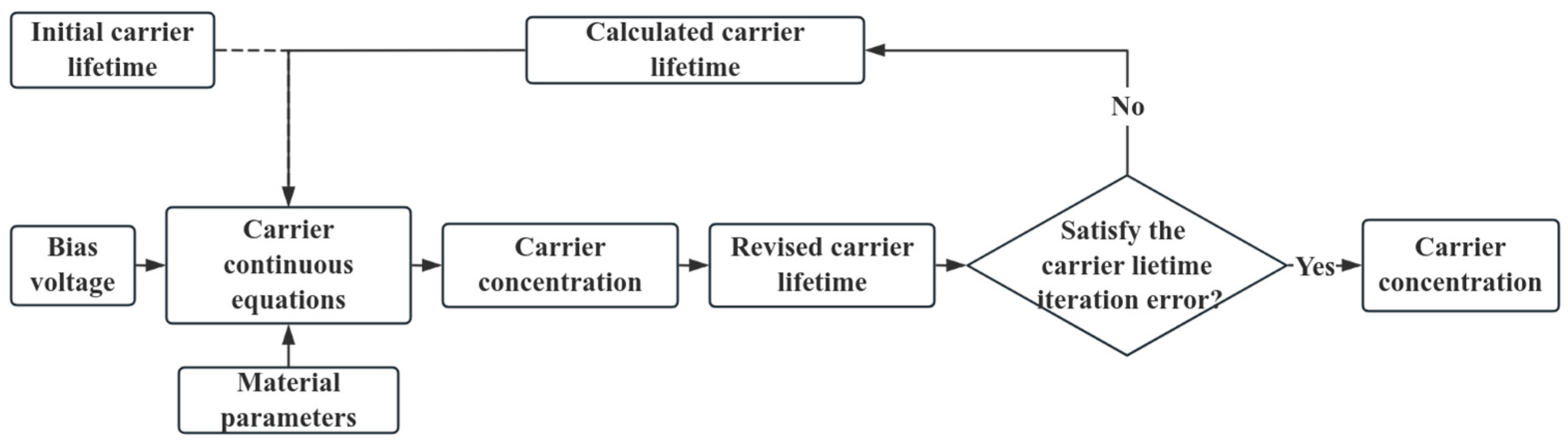
In conventional numerical calculation software, the carrier lifetime is typically set as a constant based on test results or empirical values, but constant carrier lifetime values cannot accurately characterize the carrier recombination in quantum wells under different operating conditions.
In this paper, we used a dynamic carrier lifetime iterative calculation method to calculate the carrier concentration and lifetime under different bias voltages, thereby addressing the problem that, in the carrier equation, lifetime and input voltage cannot simultaneously be treated as variables. The flowchart illustrating this calculation method is shown in
Figure 3.
The initial lifetime value in Equations (1)–(4) was assumed to be infinite, and there was no carrier recombination. We input the parameters (including the initial lifetime and material parameters) into the carrier continuity equation and solved Equations (1)–(4) for the carrier concentration. The results were substituted into Equation (5) to calculate the carrier lifetime. Then, we recalculated the carrier concentration distribution in Equations (1)–(4) based on the new carrier lifetime obtained from the last calculation. The iterations continued until the variation in the calculated carrier lifetime met the iteration error. In the iterative model, the iteration error was set such that the difference in carrier recombination lifetime at each voltage point among the last three iteration results did not exceed 1 × 10⁻¹⁴ ns. Upon meeting this condition, the final lifetime value of Equations (1)–(4) was chosen as the carrier lifetime from the last iteration.
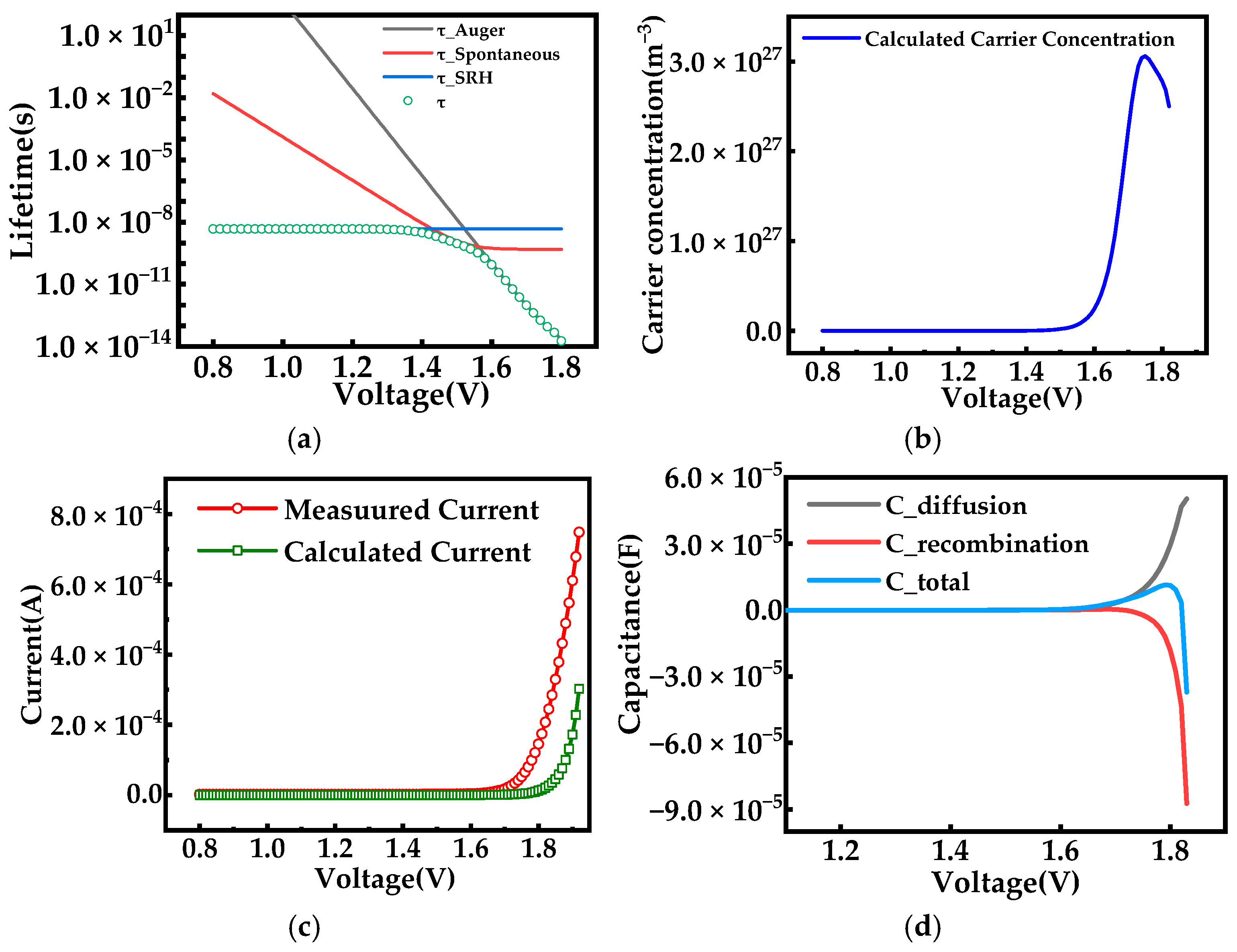
Taking the first quantum well region (
x1~
x21) as an example, the calculated electron lifetimes are shown in
Figure 4a, where the lifetime
decreases with the DC bias voltage rather than maintaining a constant value. The carrier’s spontaneous lifetime
is lowest from 1.49 V to 1.63 V, and the LED has much higher light-emission efficiency within this voltage range. Beyond a bias voltage of 1.63 V, the Auger lifetime
is minimal, and the carrier’s Auger recombination dominates the carrier recombination process, which will cause a decline in the LED’s light-emission efficiency.
Using these carrier lifetime results, we calculated the quantum well carrier concentration shown in
Figure 4b. For the carrier concentration line, there is a decline in carrier concentration after 1.6 V bias voltage due to the short lifetime and high carrier recombination.
After adding an AC small signal to the DC bias voltage, according to Equations (9)–(11), it can be inferred that the AC component
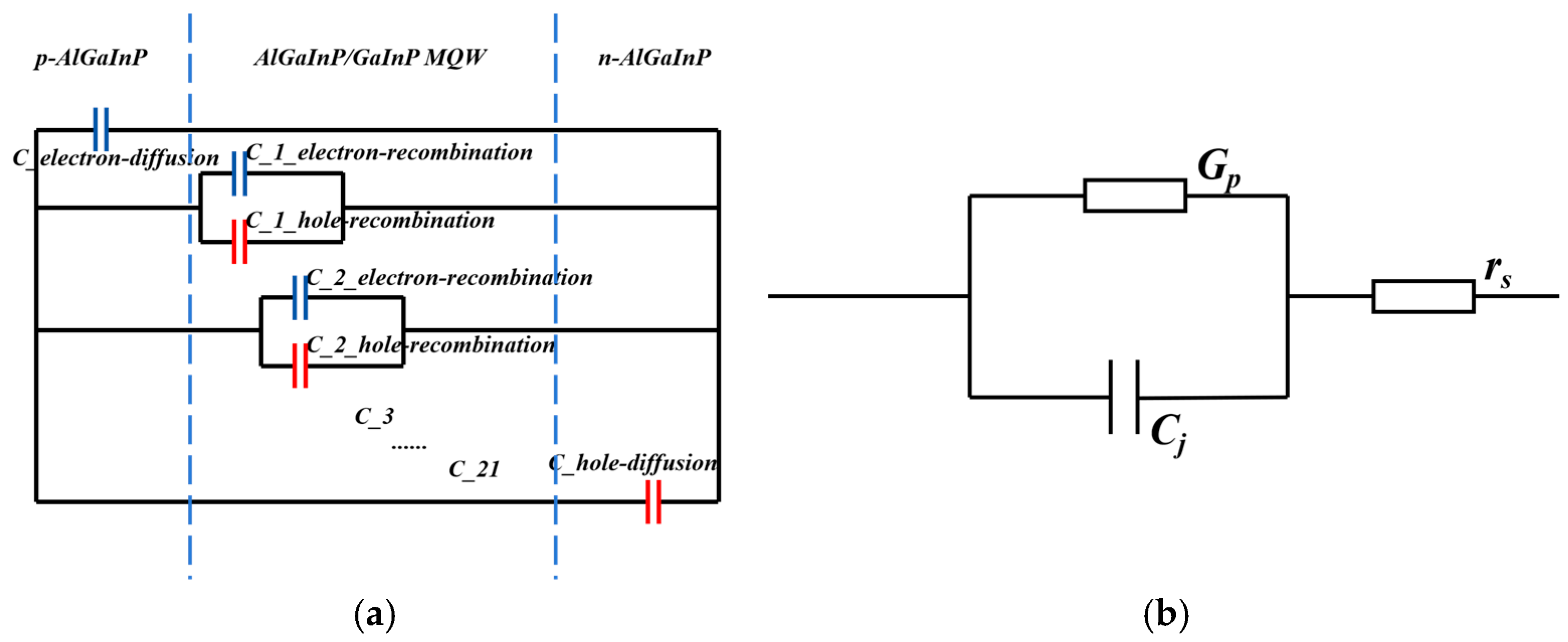
of the MQW LED is composed of the AC component of the diffusion current in the P and N doping regions and the AC component of the recombination current in the MQWs, and the capacitance comes from the imaginary part of the AC components of these two currents. Therefore, the total capacitance can be divided into P,N diffusion capacitance and MQW recombination capacitance, which is equivalent to the parallel connection of sub-capacitors in each region, as shown in
Figure 5a.
The calculated capacitances of
,
, and
are shown in
Figure 5b. Due to the carrier recombination, the
in the MQWs rapidly decreases after 1.6 V, resulting in the occurrence of negative capacitance.
and
form the total value of LED capacitance
.
Comparing the capacitance in
Figure 4d with the calculated carrier concentration in
Figure 4b, the voltage position where the NC appears remains the same as the carrier concentration decreases. It can be theoretically verified that the NC of the LED mainly comes from the recombination of carriers in the MQWs, which conforms to the situation of
.
Unlike the equivalent electrical model of an LED [
14] as shown in
Figure 5b, this paper establishes a capacitance model based on the generation and recombination of carriers within the quantum well from a microscopic perspective. The neglect of series resistance
and shunt conductance
is the reason for the calculated current being less than the measured current, as shown in
Figure 4c. The relationship between current and voltage drop under the equivalent electrical model of an LED is expressed as follows:
where
,
is the saturation current, and
n is the ideality factor.
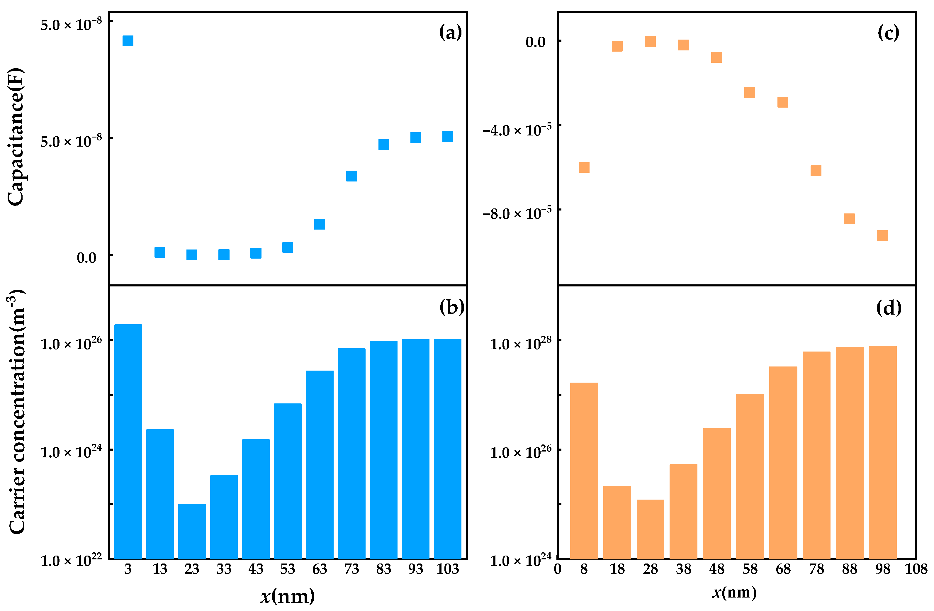
Further analysis of the capacitance within the MQWs (
Figure 6a–d) shows the calculation results of the capacitance and carrier concentration of the MQWs’ barriers and wells under a DC bias voltage of 1.85 V. Due to the spontaneous recombination, the carrier recombination intensity in the GaInP well is higher than that in the AlGaInP barrier. So, there is a negative capacitance in the well region, while the capacitance is positive in the barrier regions, and the higher carrier concentrations correspond to a higher absolute value of NC. This can mainly be attributed to the short carrier lifetime and higher electron–hole recombination rate in the high-carrier-concentration region.
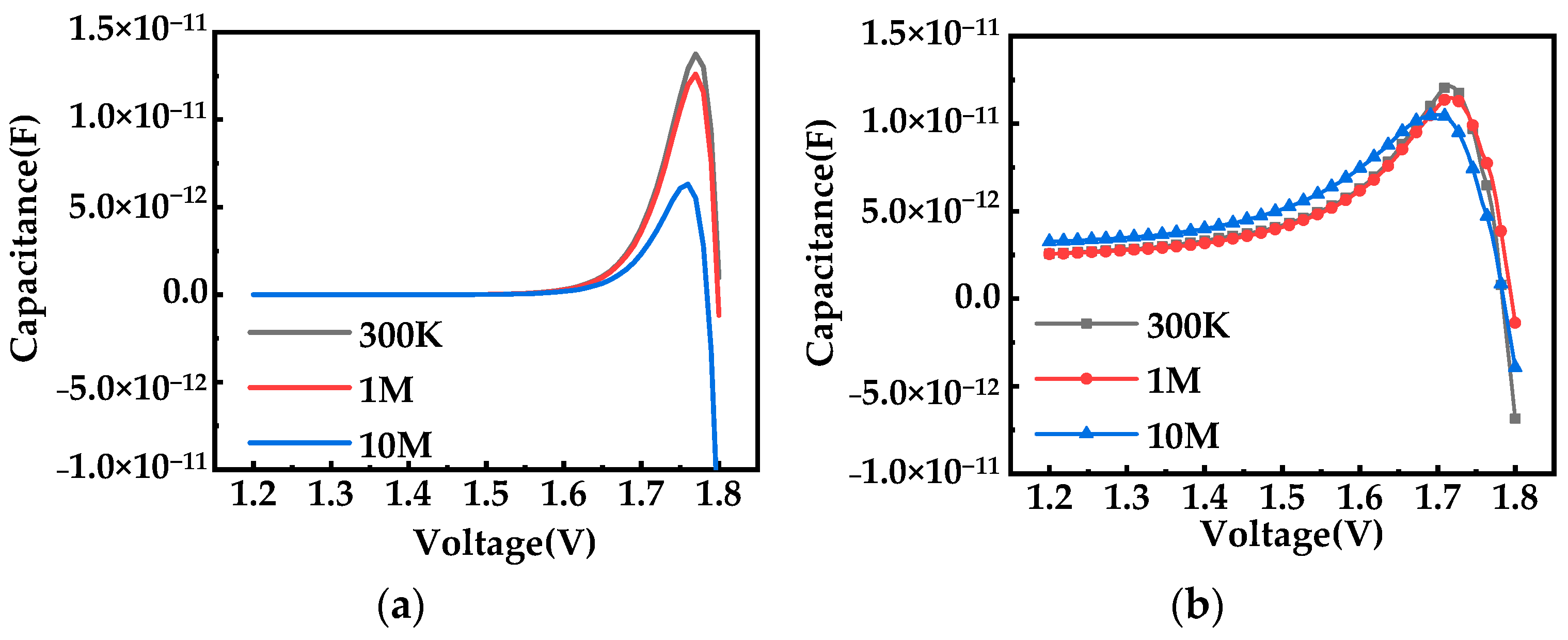
The relationship between the capacitance and frequency of LEDs under AC operating conditions was also analyzed.
Figure 7a shows the calculated capacitance–voltage curves at different frequencies, which indicate that the NC characteristics of the LED weaken under high-frequency conditions. This weakening can primarily be attributed to the influence of frequency on the effective carrier lifetime.
Taking the electron lifetime as an example, under AC conditions, the electron concentration changes to
, and the steady-state Equation (2) changes into a transient-state Equation (13):
where
. Merging
and
, we can determine the electron equivalent lifetime (
) in the MQWs.
In the low-frequency range, where , as the forward bias voltage increases, the carrier lifetime decreases, indicating enhanced carrier recombination and a decrease in carrier concentration from high, and , resulting in the NC phenomenon. In the high-frequency operating range, where and , the voltage barely affects the variation in , resulting in a reduced impact of voltage on the capacitance . This leads to a flat trend in the voltage–capacitance curve and a weakening of the NC characteristics under high-frequency operating conditions.
In this paper, the capacitance of the LED used in the calculation model was also tested using the Keithley 4200A (Tektronix, Tiangong University, Tianjin, China). The measured apparent capacitance (
Figure 7b) exhibited a similar phenomenon of NC reduction under high-frequency operation. However, the calculated ideal capacitance value was smaller than the apparent capacitance value due to the influence of parasitic series resistance and parallel conductance [
14].
5. Conclusions
In this study, we first grew a 10-period AlGaInP/GaInP MQW LED material structure using MOCVD technology. This was then processed into individual LEDs with a mesa size of 90 × 150 μm. Then, we established a theoretical analysis model for this MQW LED and determined the carrier distribution, carrier lifetime, and capacitance of the MQW LED under forward bias voltage. Next, we established a theoretical analysis model based on the MQW LED samples, from which we derived the carrier concentrations, lifetimes, and capacitance values in the well and barrier regions within the MQW LED under forward biases ranging from 0 to 1.8 V. Therefore, the MQWs’ dynamic carrier lifetime continuous equations in this paper are more accurate than fixed lifetime calculation results.
The modeling and analysis results presented in this paper demonstrate that the carrier lifetime undergoes dynamic changes under the influence of differing carrier concentrations in both the potential well region and the potential barrier region, as well as due to the application of an external forward bias. Based on the calculations of the dynamic carrier lifetime, the distribution of carrier concentrations in the multiple quantum wells exhibits an initial increase followed by a decrease. This phenomenon is caused by efficient radiative carrier recombination, and the results of the carrier concentration analysis are close to the actual carrier variations observed in the device.
Our dynamic carrier lifetime iteration method provides a decoupling scheme for carrier lifetime and input voltage, which solves the problem that carrier lifetime and electric field cannot simultaneously be variables in the carrier continuity equation. Currently, widely used device modeling software can only set the carrier recombination lifetime within the device to a fixed value and is unable to accurately characterize the carrier recombination lifetime in various regions of multi-period quantum well devices in detail. Through this model, we solved for the carrier lifetimes in various regions within the MQWs, with an iterative error of less than 1 × 10⁻¹⁴ ns. The solution method of this model is applicable to micro- and nano-sized LEDs with MQWs of any period.
Based on the AlGaInP/GaInP MQW LED carrier concentration calculation, our model exhibits the NC phenomenon starting at 1.75 V, which is consistent with the test results obtained from actual samples, and we can confirm that the NC phenomenon of MQW LEDs is closely related to the recombination in the MQW region. Our capacitors’ equivalent circuits showed that the LED’s total capacitance can be divided into P,N diffusion capacitance and MQW recombination capacitance. Each quantum well’s electron capacitance and hole capacitance contribute to the LED’s negative capacitance.
We measured the capacitance characteristic curves of the samples within the frequency range of DC to 10 MHz, and we selected representative frequencies of 300 kHz, 1 MHz, and 10 MHz for detailed analysis. The measured and calculation results also showed a weakening of the NC characteristics under high-frequency AC operation conditions of the LED. Our analysis indicates that this is because the equivalent lifetime of carriers is a frequency-related variable and remains constant as the voltage changes.
In summary, the carrier distribution and capacitance of MQW LEDs are closely related to the carrier lifetime, which is modulated by the operating voltage and frequency of the LED device. This work can provide a reference for the device modeling of LEDs in display and communication applications. For instance, in higher-frequency LED optical communication applications, negative capacitance characteristics can affect the high-frequency response of the devices. Based on the device negative capacitance analysis method mentioned in this article, precise control of the device’s capacitance can be achieved to match the frequency response of specific-frequency communication systems.


 ,
, 
