1. Introduction
In recent times, we have witnessed a continuous increase in the number of active elements in integrated circuits (ICs), particularly evident in microprocessors, which contain several billion transistors [
1]. Related to this is the steady increase in power density and the parallel issue of high local temperatures causing chips to overheat, thus leading to damage. It is a good idea therefore to install a small sensor inside integrated circuits to monitor the temperature [
2]. There are various temperature sensor designs available [
3,
4,
5,
6], one of which is a Proportional to Absolute Temperature (PTAT) sensor [
7,
8,
9,
10].
A PTAT sensor consists of several transistors and can be installed very close to potential hotspots on the IC. Its linear dependence on temperature change is an advantage that simplifies the reading of the output signal. The authors of this article designed a sensor consisting exclusively of metal oxide semiconductor (MOS) transistors, which is important because almost all microprocessors and microcontrollers are manufactured using complementary MOS (CMOS) technology [
11]. In our previous article [
12], we characterised a PTAT sensor designed using CMOS technology during the first conducted test session, but in this article, we expand upon our analysis of the same sensor. We will also analyse other closely related circuits, such as a bandgap reference (BGR) [
13,
14,
15]. These types of circuits include PTAT and Complementary to Absolute Temperature (CTAT) sensors, which provide a stable constant voltage at the output and can serve as a reference voltage for other circuits.
Several notable solutions for voltage references can be found in the literature. In [
16], a voltage reference based only on NMOS transistors is described. The structure is simple, comprising only three transistors, and provides a stable reference voltage of 171.5 mV. The authors achieved excellent reference voltage stability, but used modified transistors with different substrate dopant concentrations to design this circuit. Another work [
17] presents some modifications to the work presented in [
16], in which only five transistors with very low power consumption are utilized. The circuit also boasts an excellent reference voltage stability of 170 mV. However, in that case, it was also necessary to use transistors with modified substrate doping. In contrast, using our technology, it is not possible to use transistors with modified substrate doping, this being true for all transistors.
In [
18], a voltage regulator based on a current–voltage mirror is presented. The authors achieve high voltage regulator stability and use an operational amplifier with an MOS transistor. The regulator operates in a voltage feedback loop, which stabilizes the output voltage in the regulator, a solution often used in bandgap references. In our BGR, we used a similar solution and also achieved excellent output voltage accuracy in simulations.
Both of our circuits (PTAT and BGR) were designed and manufactured using CMOS technology at the Łukasiewicz–Institute of Microelectronics and Photonics in Poland [
19] (formerly Institute of Electron Technology). They are integrated into a larger integrated circuit together with other circuits, such as an analogue-to-digital converter, a set of current sources and mirrors, and a neutron particle detector. All designs form an application-specific integrated circuit (ASIC) that will answer the question of whether the technology used is stable, and ensures repeatable results of the circuits used.
3. Measurement Results
In this section, we present the measurement results for the aforementioned sensor. All measurements were made in a Binder MKF 115 thermal chamber [
22]. The results presented in
Figure 6 (second test session), and
Figure 7 (third test session) are for readouts taken every 1 °C.
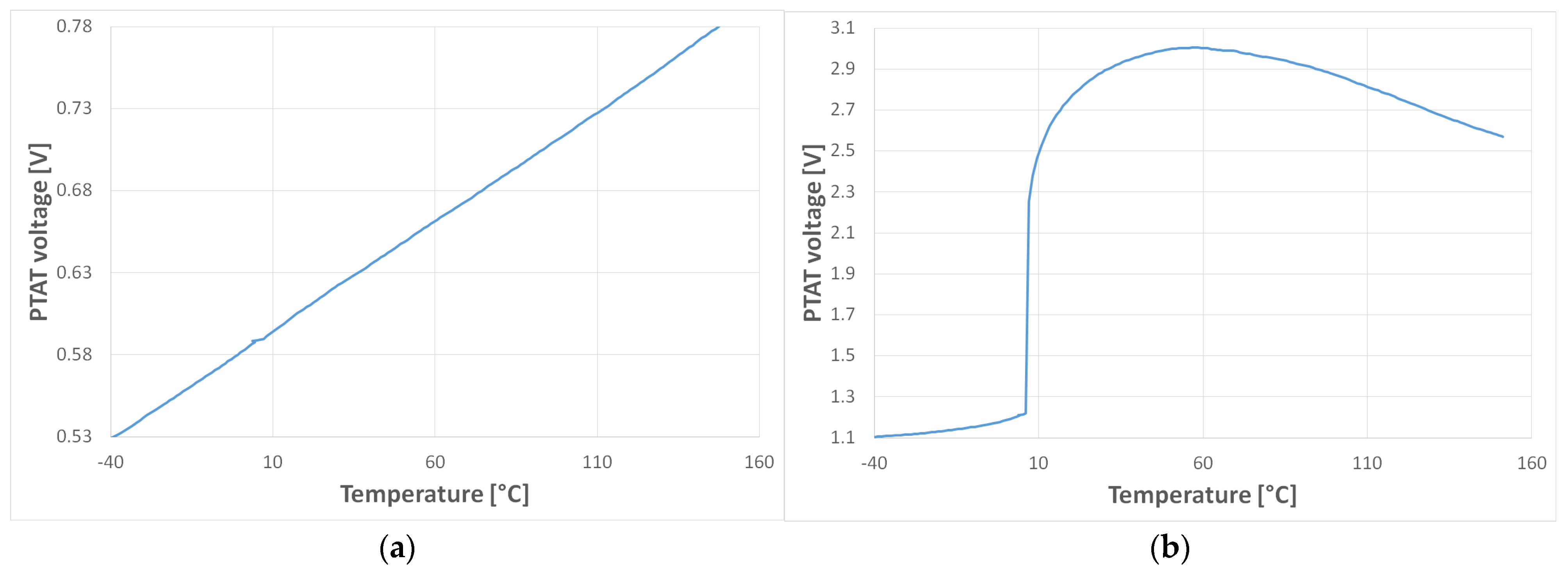
Figure 6a shows an excellent linear relationship between the PTAT output voltage and temperature. However, at a temperature of approximately 10 °C, we observe a slight dip.
Figure 6c shows the moving average (brown dotted line). This is related to the influence of other circuits on the ASIC. Such slight irregularities are more visible in the case of the bandgap reference, where a huge change in the output voltage can be seen (
Figure 6b). Observing the moving average curve of the BGR output voltage (
Figure 6d), we can also see this effect.
Moreover, the same coincidence between the PTAT output voltage disturbance and collapse of the bandgap operation can be observed for other tested IC specimens, an effect that suggests a common cause for the observed effects. The observed coincidence is very consistent over a wide range of IC specimens. Moreover, the disturbance/collapse of the circuit operation occurs for different temperatures in the case of different IC specimens. This effect is barely visible for the PTAT output voltage (
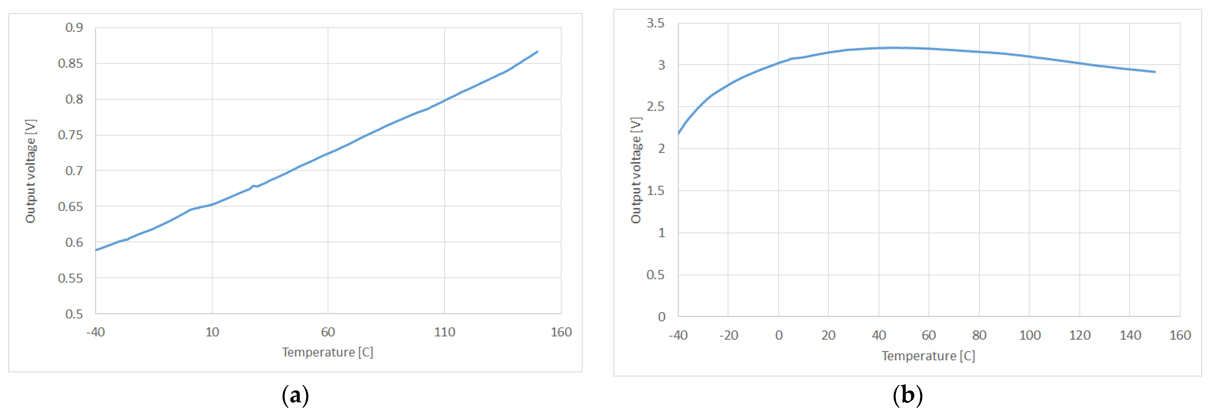
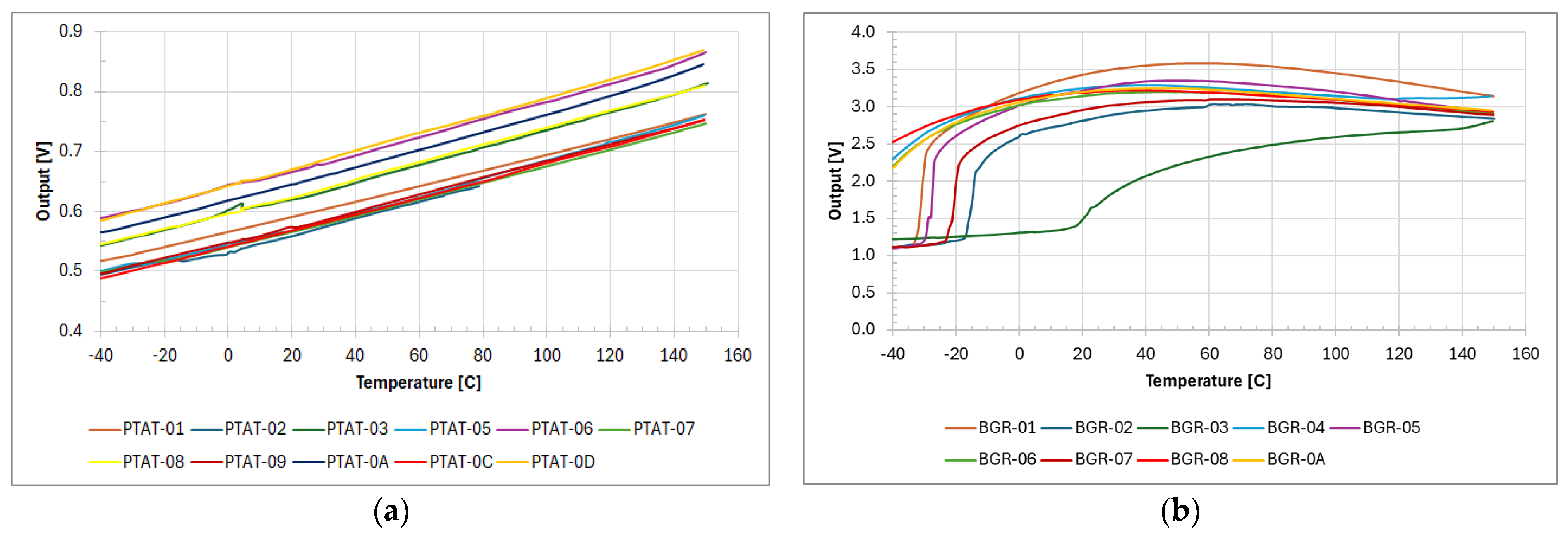
Figure 7a), but is very pronounced for the bandgap circuit (
Figure 7b). This observation excludes the possibility of an external influence, e.g., from the measurement setup, where the climate chamber would be the main suspect. As shown in
Figure 6a and
Figure 7a, an incremental analysis of the PTAT sensor voltage is required to clearly show the disturbance of this voltage increase with a temperature rise. Generally,
Figure 7 shows the results of another series of tests taken for the same chip. As can be seen, the PTAT sensor output voltage (
Figure 7a) is slightly higher than the voltage shown in
Figure 6a. Comparing the bandgap reference (
Figure 6b and
Figure 7b), it can be seen that the output voltage starts at 2.2 V and stabilizes at around 3 V. In the first case, the bandgap reference only works at low temperatures, but in the second case, it does not work at all. The results presented in
Figure 6 and
Figure 7 were obtained for the IC powered with different power supply devices, which may result in slightly different supply voltage levels. The results obtained indicate a strong influence between the circuits inside the ASIC. Since most of them are analogue, the operation of each is highly sensitive to various conditions, e.g., deviation of the CMOS process parameter, which were suspected in the PTAT sensor analysis [
23]. We decided therefore to take a closer look at the bandgap reference, and this analysis is described in the next section.
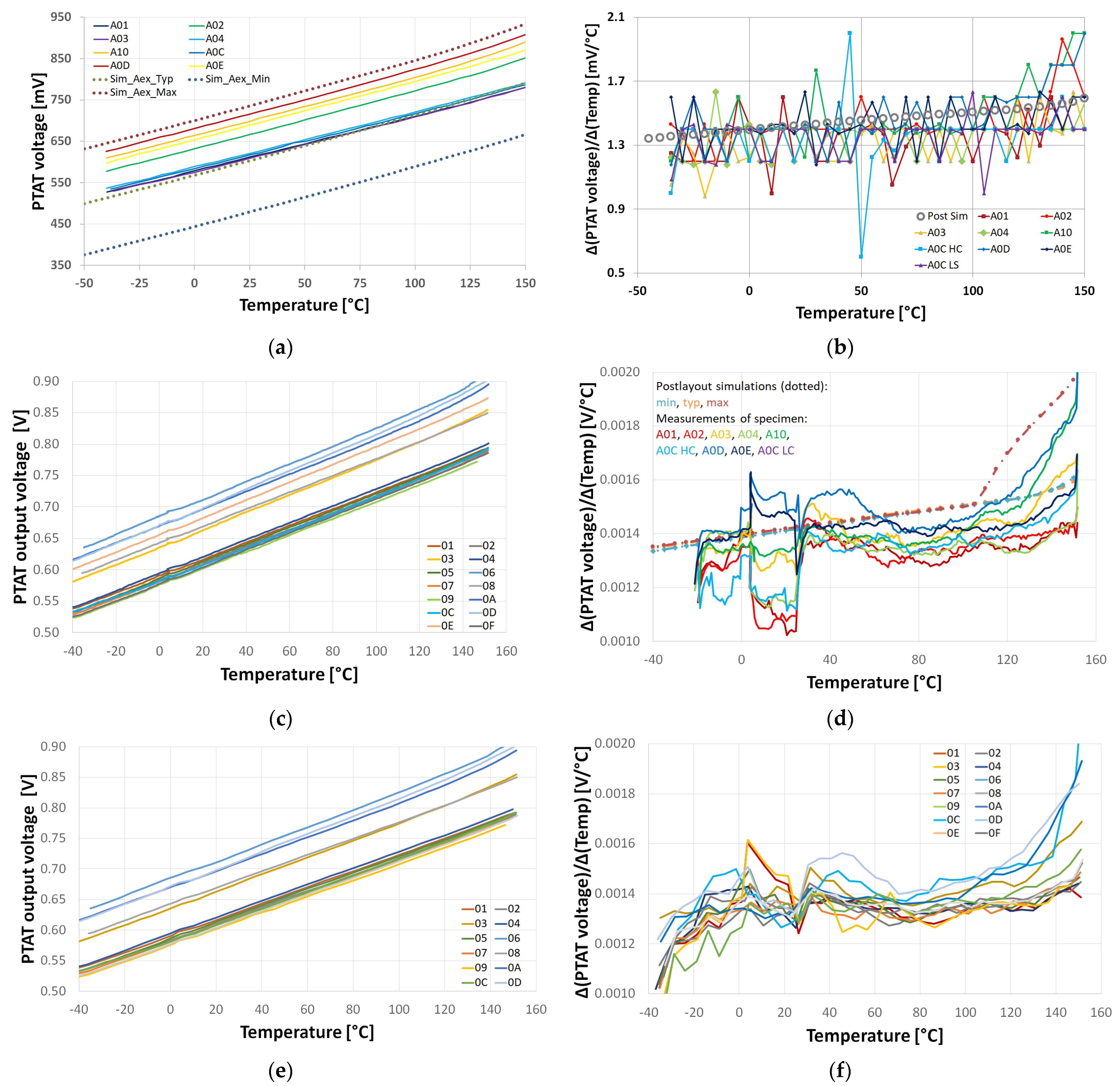
Figure 8 presents the results of the first and second series of tests presented in [
12] and [
23], respectively. The measurements presented in
Figure 8a were taken every 5 °C and with less precise measurement instruments. The potential problems that could be encountered via the PTAT operation are observable in
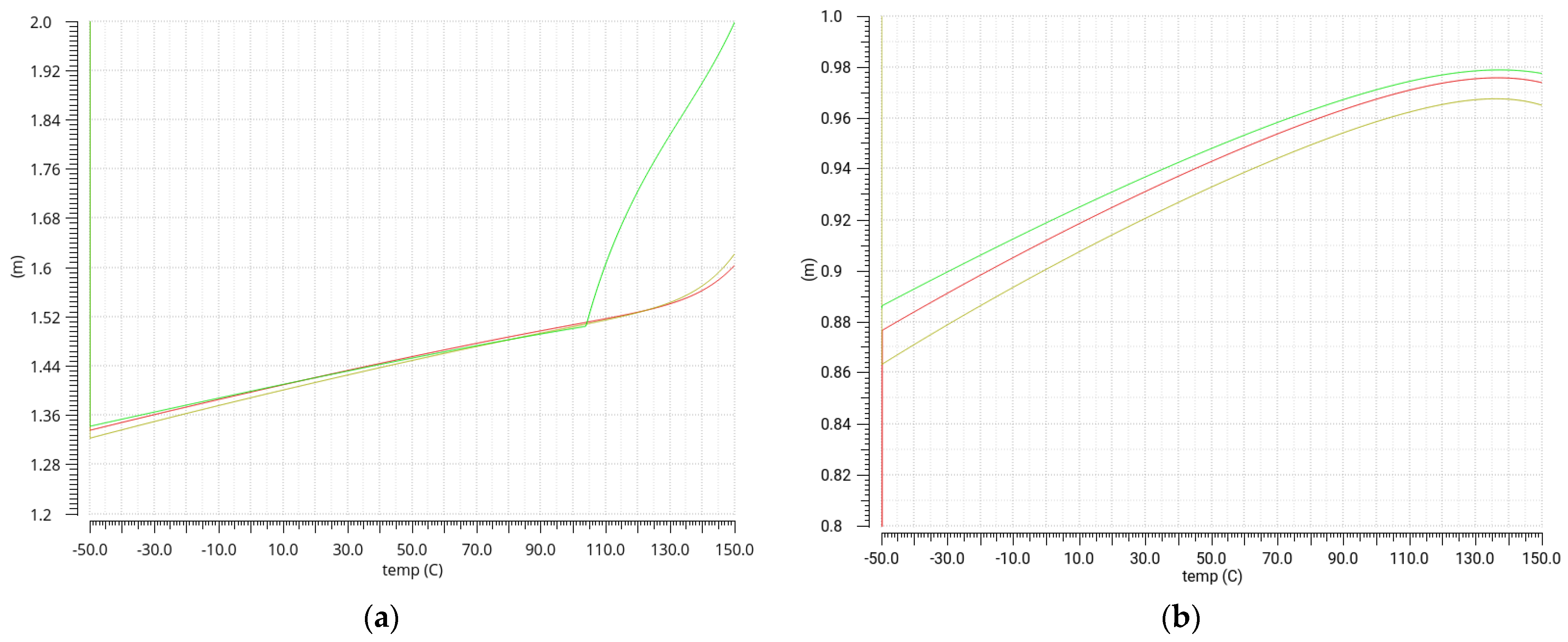
Figure 8a, though barely. Namely, an excessive increase in the voltage can be observed for very high temperatures (120 °C ÷ 150 °C) for a few specimens. The limited resolution of the measurement instruments is clearly observed in the incremental analysis shown in
Figure 8b. This effect was recreated in the simulations (
Figure 3a) relating to the improper operation of one of the PMOS transistors that leaves saturation and enters the linear operation mode with an increase in temperature, which compromises the operation of the PTAT sensor [
23]. The second (
Figure 8c) and later series of tests were performed with more precise measurement instruments and readouts were taken every 1 °C. The discussed effects found during the first test session and visible in the increment curves in
Figure 8b were found and confirmed in the more precise measurements, as shown in
Figure 6c,
Figure 7c, and especially
Figure 8d. Even the shape of the obtained curves is similar to the one obtained during the simulations, which does not cross the max. corner. In
Figure 8e,f, we can see the measurements and calculations taken during the same session as in
Figure 8b,d. However, the measurement data points were included at intervals of 5 °C. The results shown in
Figure 8e are almost perfect, resembling a smoothed version of the results in
Figure 8c. However, the incremental analysis shown in
Figure 8f shows most of the effects observable in
Figure 8d. This demonstrates that presenting the increments in the PTAT circuit output voltage is a more accurate way of finding imperfections in the measured thermal characteristics of this circuit.
Generally, it can be stated that PTAT measurements taken every few degrees Celsius can obscure some phenomena that take place in this circuit. What enabled us to find an unexpected operation of the PTAT sensor was a set of measurements with high-resolution instruments used to take measurements for very small temperature intervals. Such a set of data points enabled the incremental analysis of the PTAT sensor that disclosed details of its operation and their incidence with the operation of another circuit, the bandgap, installed in the same IC.
4. Bandgap Reference Circuit (BGR)
The next circuit we analysed was a bandgap reference [
24,
25]. The BGR schematic is shown in
Figure 9.
The BGR was designed in such a manner that the output voltage is almost independent of temperature, made possible according to the usage of PTAT and CTAT references. It consists of the diodes and resistors that are responsible for the output voltage. They are connected to the operational amplifier to achieve a stable constant output voltage. The chip was powered by 5 V, so we set the output voltage to 1.26 V.
The typical relation between diode current I and voltage V
D can be expressed by the following formula [
20,
21]:
where V
T is a thermal voltage consisting of a Boltzmann constant, absolute temperature in Kelvin, and charge of the electron. After transformation, we have
In our BGR, the output voltage V
REF can be expressed via the following equation:
where
R01 =
R0 +
R3 +
R5 = 3 × 5 kΩ = 15 kΩ,
R03 =
R4 +
R12 +
R13 +
R14 +
R15 = 5 × 355 Ω = 1775 Ω, and
n = 24.
After performing those calculations, we obtain an output voltage
VREF = 1.26 V. This is confirmed by the simulation results shown in
Figure 10 (see the output voltage for a nominal power supply of 5 V). In
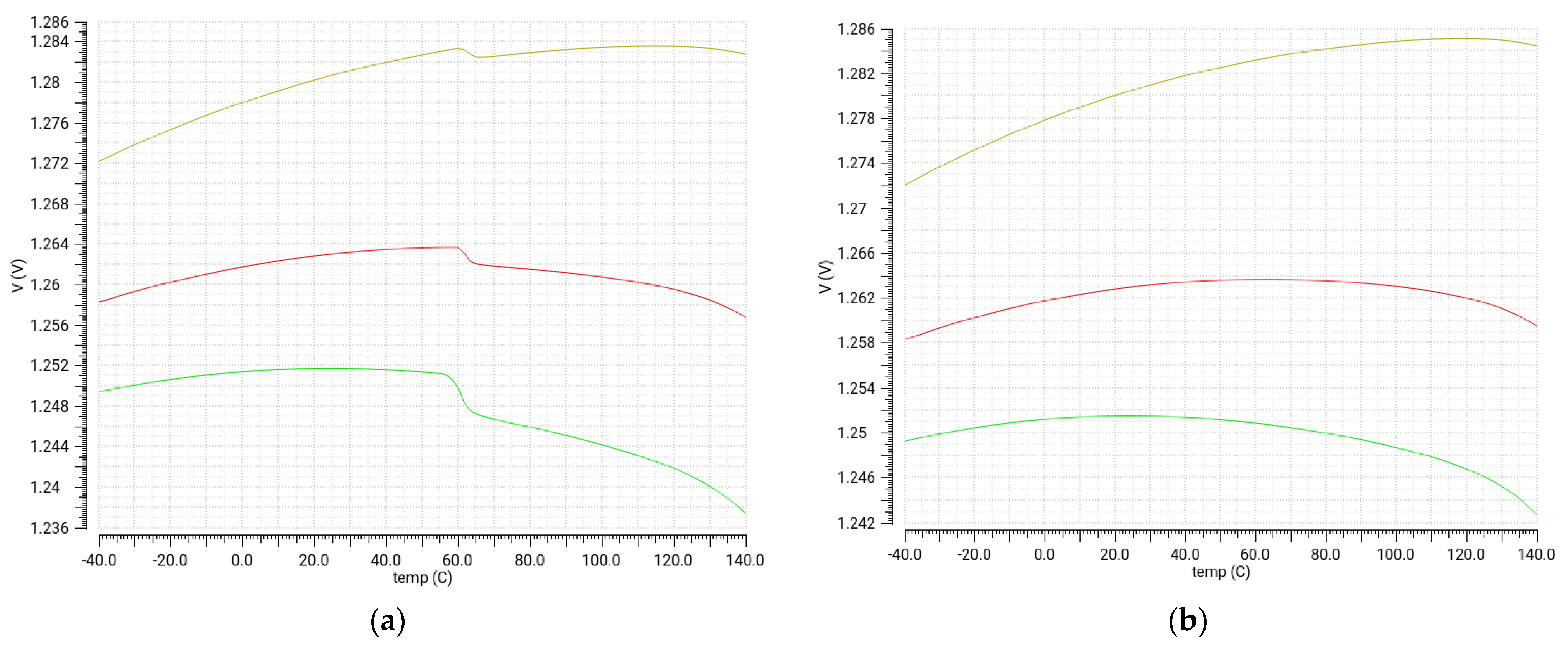
Figure 11, we can also observe the output voltage versus temperature change, but there are two curves. The first one (blue) represents the whole circuit, which contains modified memory cells. As can be seen, this leads to a voltage drop near 60 °C, which is a very small value, but should be considered during normal operation of the whole chip. If we remove a memory cell from the circuit, we observe a smooth curve (orange) which gives a very stable output voltage. In the next figure, we can see the layout of this circuit. The temperature coefficient (TC) for 25 °C is 27 ppm/°C (calculated from simulations), and the TC is 282 ppm/°C for the measurement of test specimen one.
During the whole chip analysis, it is not possible to remove the memory cell in a real ASIC. That is why we try to eliminate this unnecessary behaviour of the BGR via proper connection of the other circuits. In ASIC, we have the following circuits:
PTAT sensor;
Bandgap reference (BGR);
Analogue-to-digital converter (ADC);
Electrothermal filter (ETF);
A set of current mirrors (CM);
D flip-flop (DFF);
Memory cell.
All circuits are placed on an n-type silicon wafer, each thus having a common supply voltage (5 V) but separate grounds. This allows us to identify the proper connection to eliminate the voltage drop in the BGR output. We leave the ADC and CM mass unconnected, and these circuits thus do not influence the other circuits, especially the BGR. It turned out that the voltage drop in the BGR output disappears. Another possibility is that we can eliminate this voltage drop when we apply a small voltage to the ground pin of the BGR (approximately 20 mV). We are therefore able to obtain a smooth BGR output voltage. These two cases are visible in
Figure 12, where we can see the BGR output voltage and two ground currents (digital and analogue). In
Figure 13, we can also see the corner simulations for the BGR with (a) and without a voltage drop (b).
To establish why we saw a voltage change in the BGR, we performed a range of additional simulations not documented in this work. We added some coefficients intended to represent the resistance change in the resistors, and also a channel length of the transistors; these coefficients are connected to the diffusion spread during the manufacture of the devices. In doing so, we obtained many interesting characteristics of the BGR.
The simulations shown in
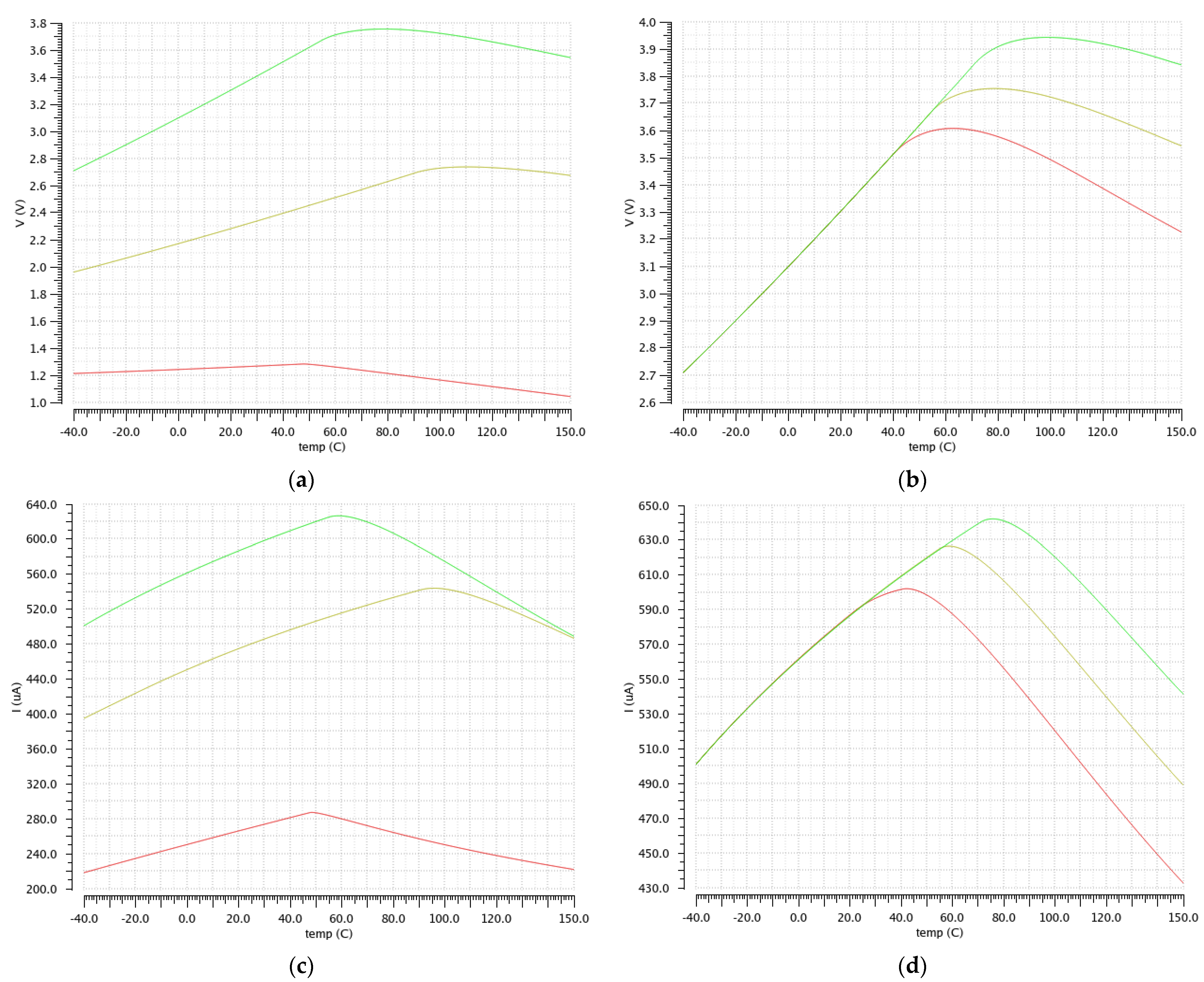
Figure 14 present an output voltage and ground current of the BGR in dependence on the temperature change. On the left side, we can see the output voltage for different values of the ‘pwell’ coefficient, which relates to the p-well doping used in transistors and resistors. It takes values from 0.5 to 2 and thus allows us to estimate the spread of the values of these resistors. It can be observed that each curve starts at a different output voltage level and increases to reach its maximum near 60 °C. After that, they start to decrease. On the right side, we can see the output voltage for different voltage supply. All curves increase from −40 °C to near 60 °C, where they reach their maximum. Next, they start to decrease. Their shape slightly resembles the output signal of the BGR.
All circuits were designed and verified using Cadence IC Design Suite version 6.1.8. [
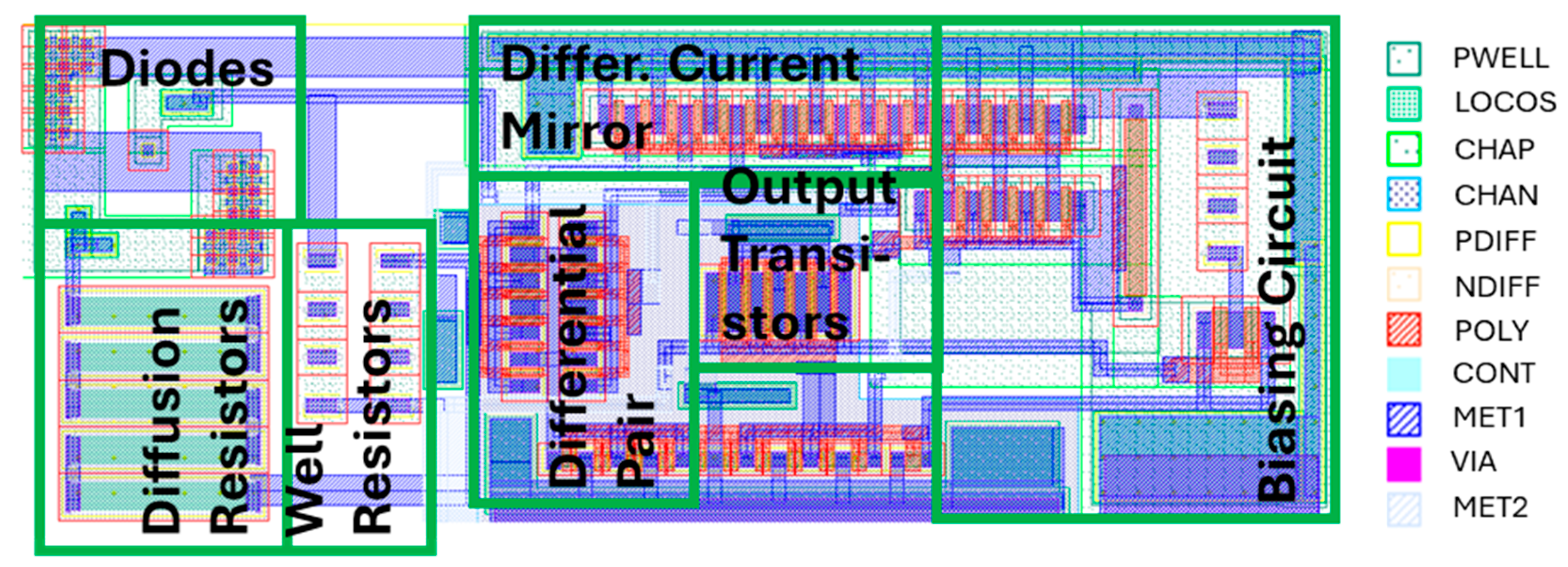
26]. The BGR layout is shown in
Figure 15. The next section is devoted to discussing the results.
5. Discussion
This article provides an extended analysis of PTAT and BGR, which were discussed in our previous article [
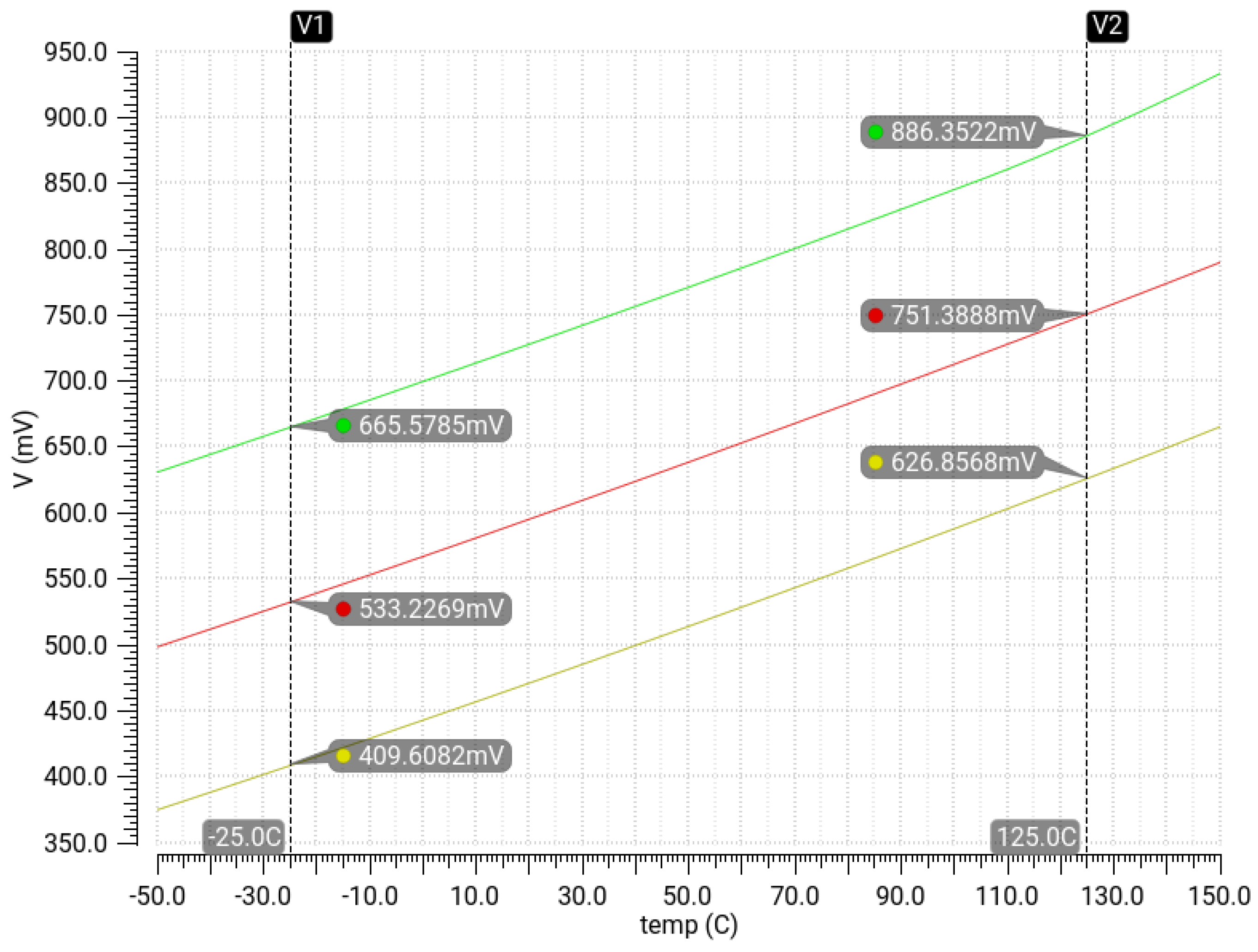
12]. The authors proposed certain modifications to the PTAT sensor to eliminate the non-linearity visible at the maximum corner (
Figure 3a—green line). The simulation after modification is shown in
Figure 3b. This non-linearity is visible in the first derivative of the output signal, but it affects the linearity of the output signal. The measurement results of the PTAT sensor are shown in
Figure 6a and
Figure 7a. An excellent linear relationship is visible across a wide temperature range (from −40 °C to 150 °C). After taking measurements more accurate than those taken initially, we see a slight drop in the PTAT sensor output voltage. The first measurements were taken with an accuracy of 5 °C, but the second ones with an accuracy of 1 °C, which indicates an undesirable effect near 5 °C. For the PTAT sensor, this does not have such a significant impact; however, for the BGR, the output voltage shows a large jump from 1.2 V to 3 V. We therefore decided to analyse the BGR next.
The results presented in
Figure 11,
Figure 12 and
Figure 13 show some drops in the output voltage and/or current of the bandgap reference circuit. The BGR was designed for a reference voltage of 1.26 V. This circuit is analysed as a whole, where we obtain a small voltage drop (2 mV) at the output at a temperature of approximately 60 °C (blue line in
Figure 11); though a very small drop, it is noticeable. This phenomenon is related to the simulated malfunction of another implemented circuitry, the memory-based particle detector. The observed effect is related to unintended activation of some transmission gate-based logic gates, due to non-optimal design of the MOS-based switches. Extra current flow slightly repolarises the supply node mesh, which causes a slight but discernible alteration of the bandgap operation. This effect was not observed in the conducted measurements, but it can serve as an example of a possible unexpected influence of a single faulty subcircuit on the ones implemented in the same IC.
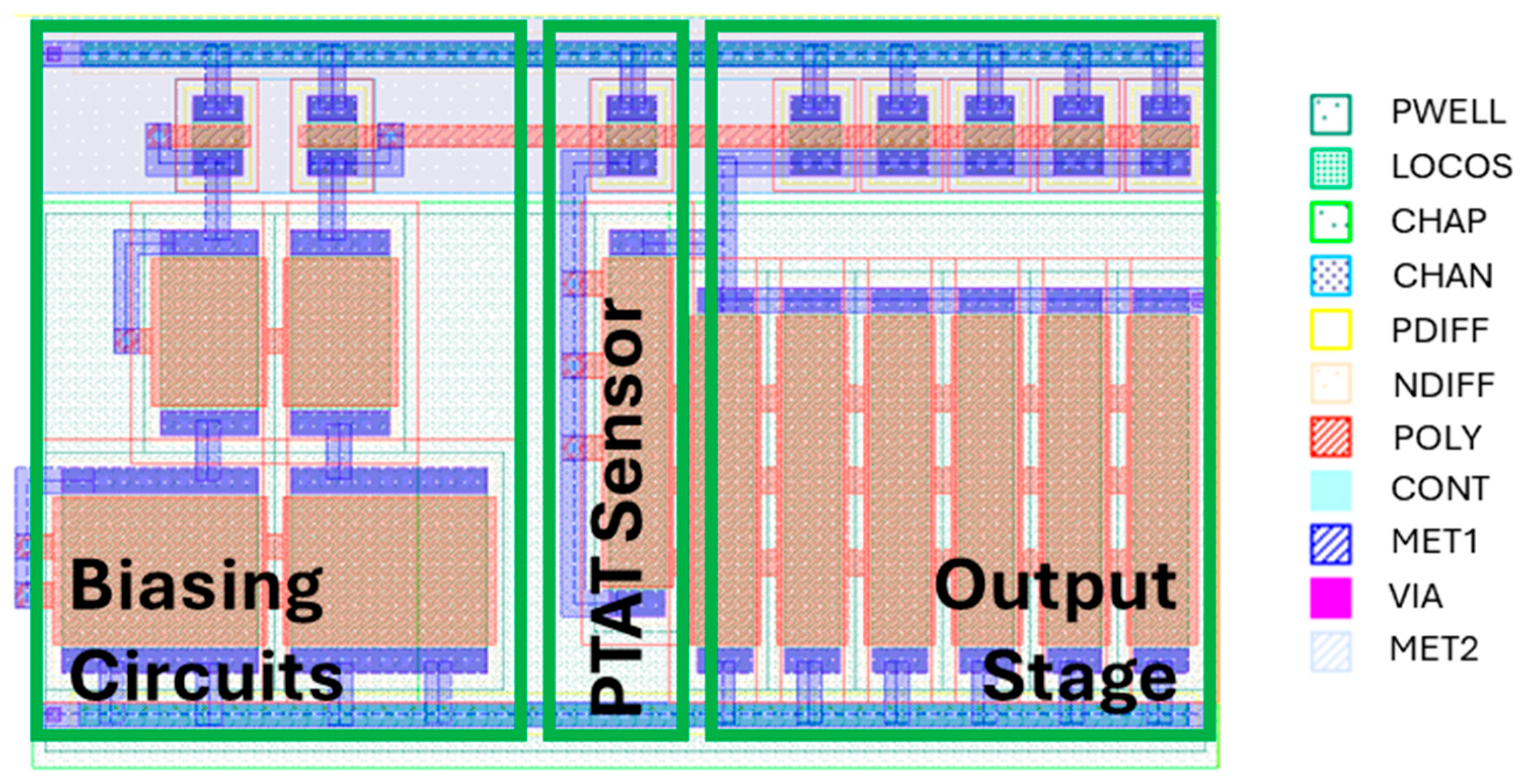
Analyses of the drawn layouts indicate that each circuit could be protected by guard rings, whose main task is to ensure adequate insulation of individual circuits. The best solution would be to place each circuit in a separate well insulated with protective rings, similar to high-voltage technologies. Another useful technique for minimising circuit malfunction is to add dummy components in layout to ensure a similar environment for the components being matched. In highly sensitive components, the common centroid matching technique is used, especially in the case of a differential pair of transistors. This will minimise the impact of the circuits on each other and improve their performance. Despite the imperfections identified in the layout, we believe that the observed bandgap reference malfunctions would not have been possible if the technological process of manufacturing integrated circuits had been completely correct.
Measurements presented in this manuscript were conducted via measurement devices that, as real devices, offer limited accuracy and precision. Furthermore, the whole measurement setup also adds to the total noise present in the measurement result. No direct noise characterization of the test setup was performed during the test sessions. Analysis of the available readouts of the measurement devices showed that the readouts are not well suited to direct noise characterization. The devices were registering voltages and currents that are expected to be taken in stable thermal conditions. However, the test PCB with the DUT ASIC was always placed in the thermal chamber. The thermal chamber was always actively controlling and adjusting conditions, and as a result, the acquired readouts always fluctuated to an extent much exceeding observable noise levels. There were attempts undertaken to select a limited temperature range for which the variability of the measured voltages could be removed by subtraction of respective trend lines, but resulting datasets have shown variability higher than the observed levels of noise.
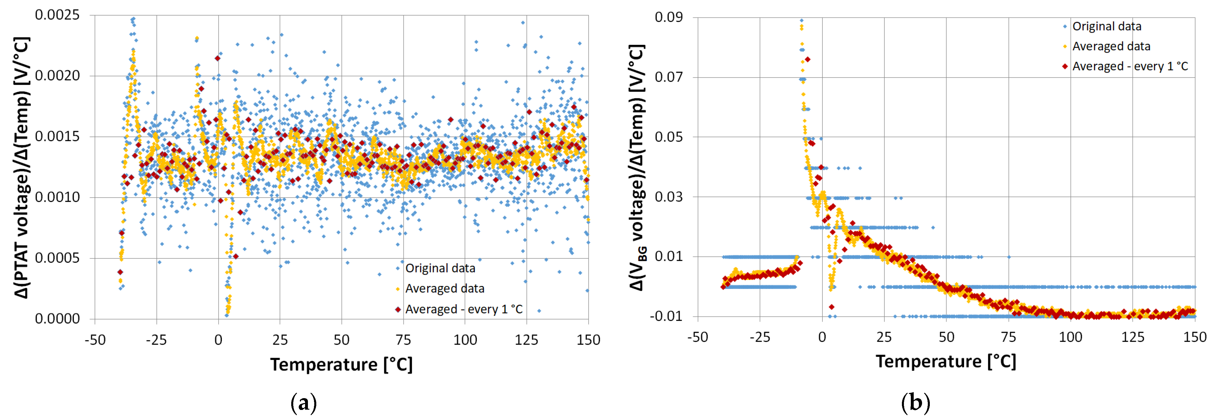
Due to such circumstances, the decision was made to present the noise influence based on increments of the output PTAT and bandgap voltage versus the temperature change. This form of presentation significantly highlights the noise presence, which is also beneficial in case of visual inspection of such results.
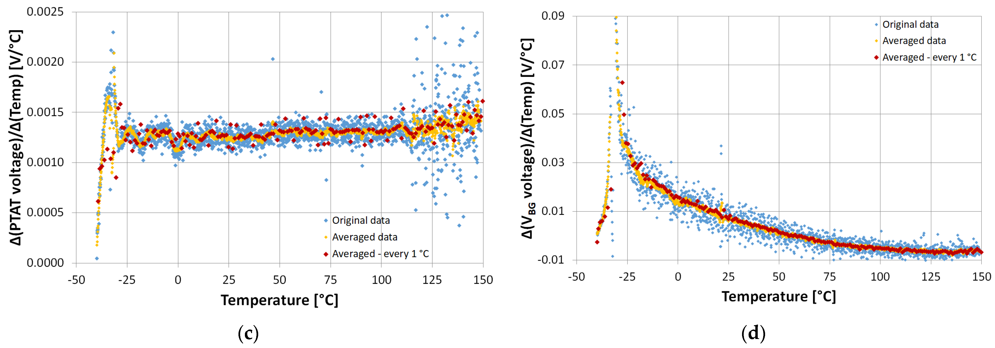
Figure 16 shows these results for the PTAT circuits (
Figure 16a,c) and bandgap (
Figure 16b,d) for one of the tested specimens (no. 1), for two different test sessions (namely, second and third, respectively).
During the experiment, measurements were taken every 6 s, which was expected to mean a readout every 0.1 °C. The idea behind this approach is to cope with the expected (and observed) noise by averaging 10 readouts around every temperature value. This is why
Figure 16 shows three datasets: original data, averaged data, and averaged every 1 °C. The final dataset presented in this manuscript is the one with averaged readouts for every integer temperature value, meaning every readout taken is used only once and influences only one final averaged value.
It can be observed that the results for the PTAT circuit are better in the case of the latter (or third) test session. This can be attributed to the refined measurement device setup and a new version of the test PCB for the DUT ASIC. For the bandgap circuit, it is clearly visible that different measurement devices were used in the second and third test sessions. The device used in the former session is Sanwa PC510a, and its limited resolution can be clearly seen in
Figure 16b. It is mainly due to initial readout averaging that the obtained results are acceptable for basic analysis. In the third (the latter) test session, the bandgap output voltage was measured with a Fluke 8846A instrument (Fluke, Everett, WA, USA), and the influence of this change on the quality of the obtained results is clearly observable in
Figure 16d.
An attempt was made to assess noise levels as a result of processing the incremental mode results. Due to shape of the obtained curves (
Figure 16), it was possible to determine temperature ranges for which good quality trend lines were found. The trend line values were subtracted from the averaged readouts for these temperature, and the mean value of the resulting values is thus (close to) zero. The obtained values were integrated using the trapezoidal rule. As the summation of the consecutive values was not performed, the values obtained were still consistently distributed around zero. The dispersion of the obtained values was visually compared to the dispersion of the readouts directly taken from the measurements and was found to be comparable. Finally, the calculated values were taken as a basis for calculating the standard deviation, as presented in
Table 1. It can be observed that standard deviation results are consistent with the results presented in the incremental form in
Figure 16.
Figure 16b shows that a single deviation value does not reflect the limited resolution of the meter used for the bandgap measurements in the second test session.
Regarding real BGR measurements, a slightly different phenomenon can be observed. Some BGR specimens only work well at lower temperatures. However, at higher temperatures, the output voltage increases to 3 V (
Figure 17b). It is difficult to explain how these circuits work. However, some scenarios based on problems with the technology process have been tested to try and recreate the observed phenomena.
Each of the circuits affects another circuit in the ASIC design, as they are manufactured on the same n-type substrate. According to our research, the spread of parameters, especially the diffusion of p-type, also has a significant impact on the operation of both circuits. In this technology, diffusion is the most critical technological step, as previously reported by employees of the Łukasiewicz–Institute of Microelectronics and Photonics in Poland [
16]. When designing analogue circuits, we must therefore allow for a large margin of parameter variation in the manufactured circuits via sufficiently robust circuit design.
According to the authors of [
27], who studied similar technologies, 0.35 µm and 180 nm both have comparable performance for NMOS and PMOS devices. However, it is known that as device dimensions decrease, analogue devices become more difficult to design correctly due to parameter spread. In general, this is a trade-off between frequency response and increased short-channel effects, with differences in mobility between electrons and holes becoming less significant at smaller geometries due to velocity saturation effects [
28].
The simulations presented in
Figure 14 show that deviation of process parameters, such as diffusion and well doping, can cause effects similar to those observed in the band gap measurements presented in
Figure 17b, with the exception of abrupt collapse of the proper band gap operation, visible for some specimens in
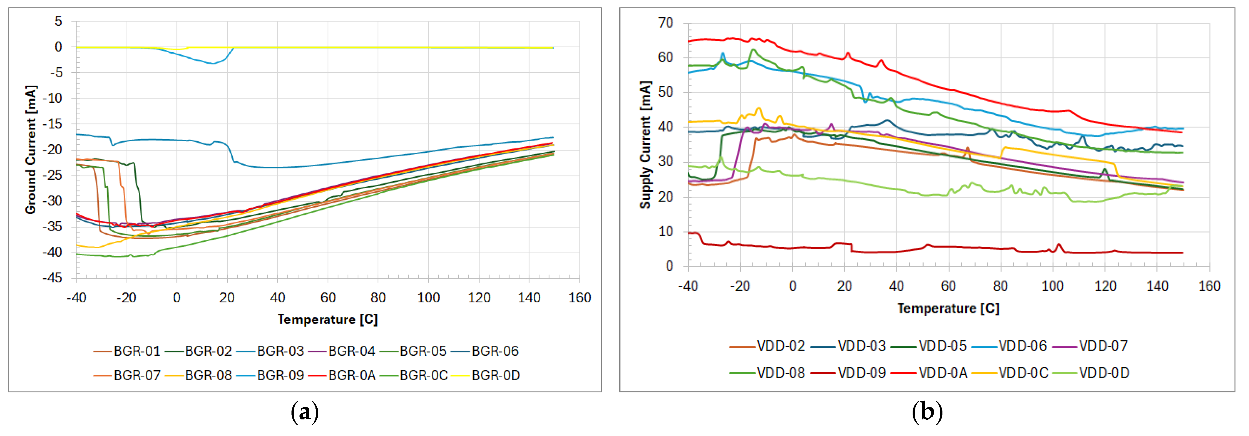
Figure 14. Furthermore, the measured current flow through the bandgap circuit shown in
Figure 18a indicates its significant change when the bandgap operation collapses.
Figure 18b shows that current consumption of the bandgap is a significant part of the current consumption of the whole IC. The collapse of the bandgap operation thus caused a significant change in load of the IC supply nodes. This may lead to a change in voltage drop in the supply and ground nodes, which can also cause limited local changes in substrate and well biasing. These effects may be responsible for the observed limited disturbance in the dependence of the PTAT sensor voltage on temperature.
Table 2 compares some BGRs with our design. However, the technology selected is not the latest, so we chose some parameters according to which our sensor is an interesting design. While there is a very wide temperature range or a temperature coefficient, unfortunately, we must interpret the simulation results here, as most of the BGR systems that were measured operated only at low temperatures (below 20 °C). It should be noted that the mentioned simulations were conducted with resistor models manually equipped with thermal coefficients.
6. Conclusions
This manuscript presents an extensive analysis of a PTAT sensor, with particular emphasis on the linearity of the output voltage. After introducing minor modifications, we achieved excellent linearity, which is particularly evident in the corners of the sensor response curve; these modifications are clearly visible in the corner analysis. The increase in voltage for the maximum corner (
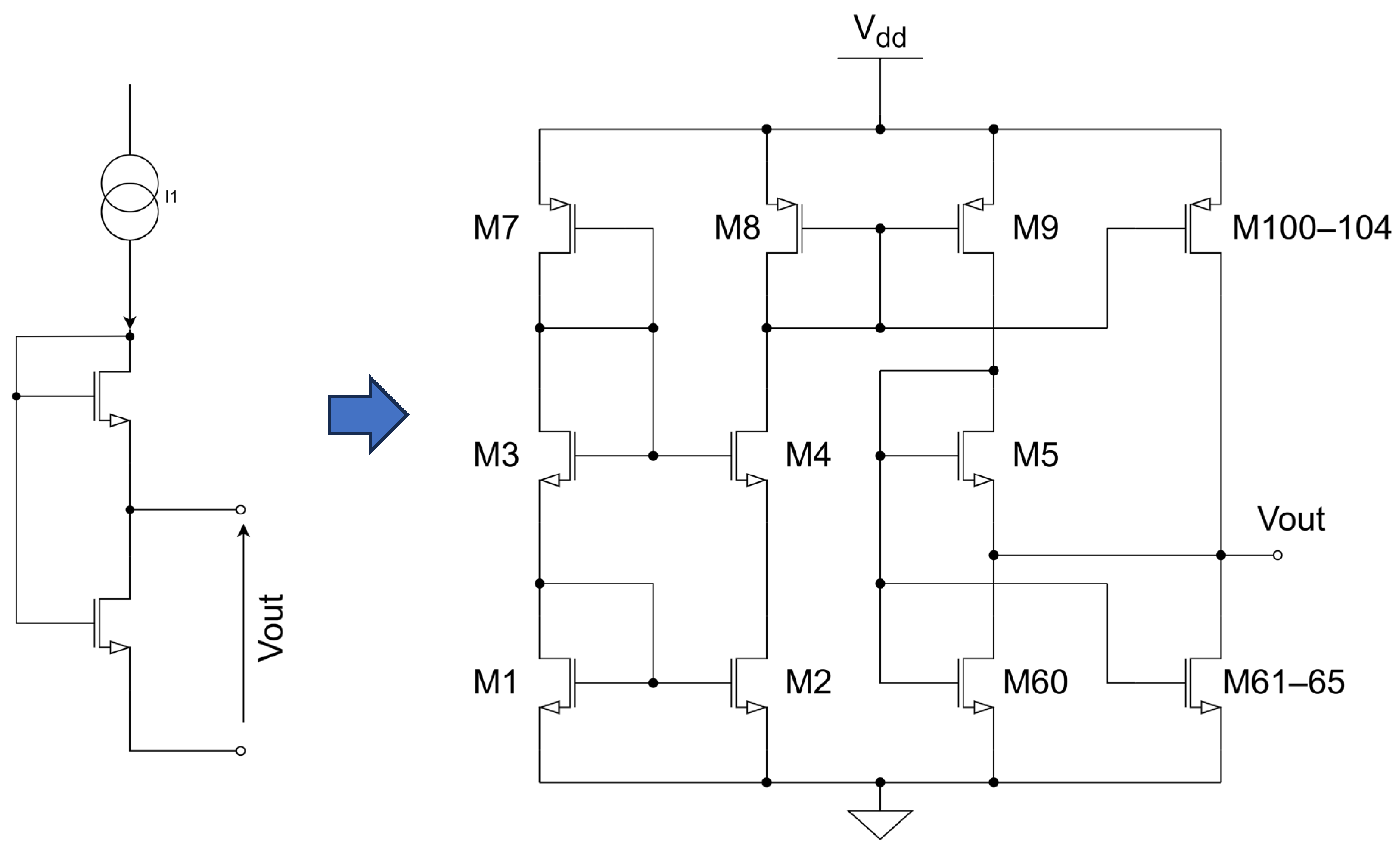
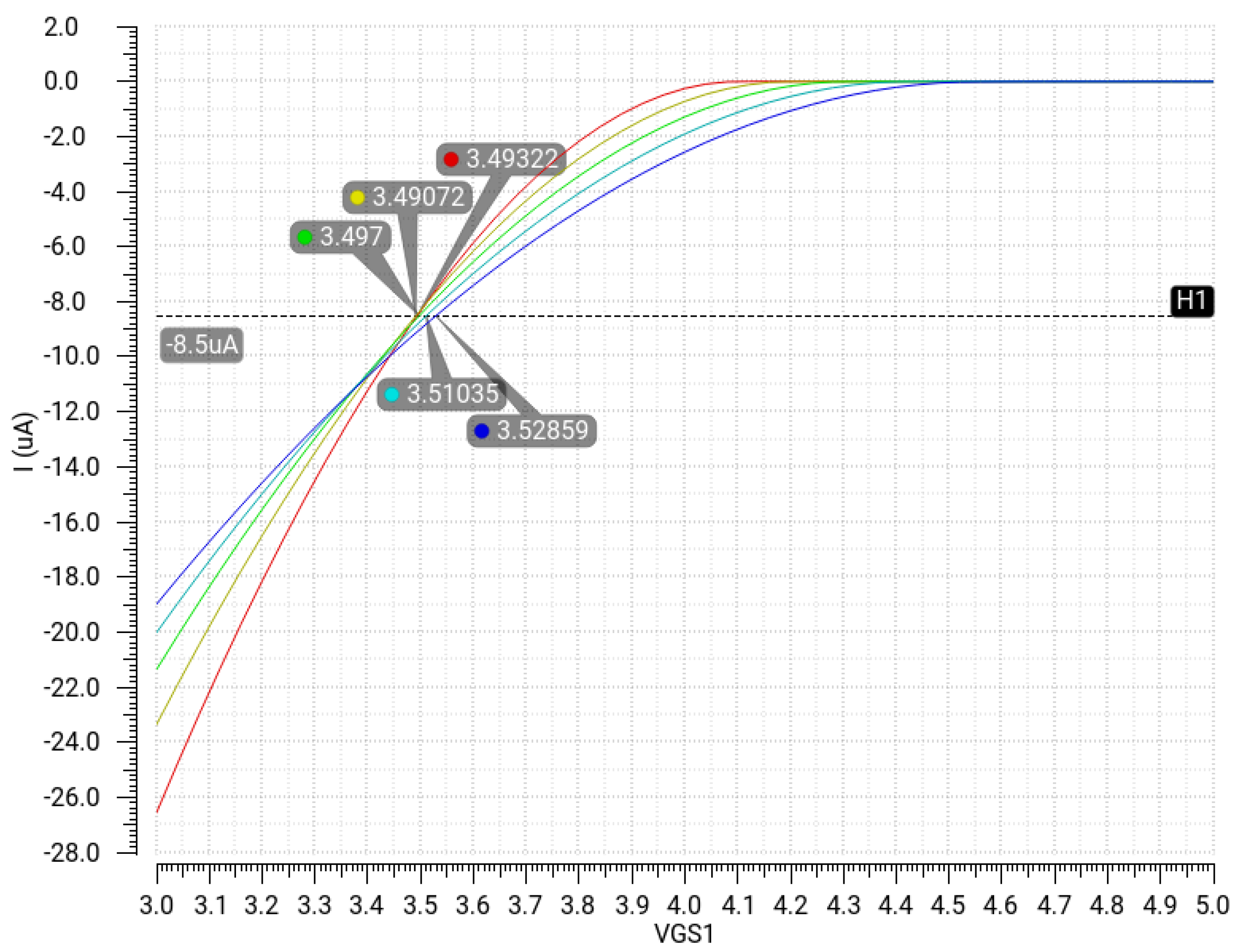
Figure 3) was compensated for by a slight change in the input current flowing through the PTAT core transistors from 8.5 µA to 4.25 µA. This change has little effect on the sensitivity of the sensor, which decreases slightly (see
Section 2.3). According to the BGR analysis, we can see that the output voltage is stable, but near 60 °C, we observe a slight drop in voltage, which is related to the memory cell circuit inside the ASIC. We cannot remove the memory cell from the actual integrated circuit, but we can eliminate this unnecessary behaviour by appropriately connecting other circuits.
The described ASIC, which contains several different analogue circuits, demonstrates that it is very difficult to implement these circuits on a single common substrate without mutual interaction. However, we designed all circuits with particular attention to the separation of individual circuits and observed slight differences in the output signals. Since the selected technology uses n-type silicon, we designed each block with a single power supply but with different grounds. The preliminary results of the measurement show that the PTAT sensor works very well. The BGR, on the other hand, exhibits some undesirable behaviour, as it works correctly at low temperatures, but at higher temperatures, its output increases and settles at 3 V (
Figure 17b). In simulations, we observed a slight drop in output voltage, which is related to the non-zero resistance of the ground connection of all blocks in the ASIC.
In our opinion, and following discussions with the employees of the Łukasiewicz–Institute of Microelectronics and Photonics, p-type ion implantation may have the greatest impact on the design of analogue circuits. Structures related to this process are found in many types of simple devices, such as transistors, diodes, and some resistors. The stability of circuits, especially bandgap references, in which we have p-type resistors, is highly sensitive to this process. Other circuits, such as PTAT, which only have transistors (mainly in symmetrical and matched configurations), are less sensitive to the parameters of this process. We can therefore conclude that fluctuations in the technology process, such as p-type ion implantation, which lead to problems with the operation of a single block of the designed IC, influence the operation of the whole IC.
The key to finding the aforementioned disturbance was a repeated test session with much higher-precision measurement instruments and a largely reduced temperature step. These improvements, paired with an incremental analysis of the derivative of the PTAT output voltage versus temperature, finally identified the phenomenon. Further tests of supply and ground node current consumption enabled further investigation of the unexpected PTAT sensor behaviour and led to the most probable culprit.
It should be noted that excessive voltage drops in the supply and ground nodes may lead to modified polarization of the substrate and well area, which may also lead to alteration of the implemented analogue circuit operation.
