Article

A Low-Power SNN Processor Supporting On-Chip Learning for ECG Detection

1
College of Integrated Circuits, Zhejiang University, Hangzhou 311200, China
2
College of Computer Science and Technology, Zhejiang University, Hangzhou 310027, China
*
Author to whom correspondence should be addressed.
Electronics 2025, 14(24), 4923; https://doi.org/10.3390/electronics14244923
Submission received: 13 November 2025 / Revised: 9 December 2025 / Accepted: 10 December 2025 / Published: 15 December 2025
(This article belongs to the Section Semiconductor Devices)

Abstract

Traditional ECG detection devices are limited in their development due to the constraints of power consumption and differences in data sources. Currently, spiking neural networks (SNNs) have quickly attracted widespread attention owing to their low power consumption enabled by the event-driven nature and efficient learning capability inspired by the biological brain. This paper proposes a low-power SNN processor that supports on-chip learning. By implementing an efficient on-chip learning algorithm through hardware, adopting a two-layer dynamic neural network architecture, and utilizing an asynchronous communication interface for data transmission, the processor achieves excellent inference and learning performance while maintaining outstanding power efficiency. The proposed design was implemented and verified on Xilinx xc7z045ffg900. On the MIT-BIH database for ECG applications, it achieved an accuracy of 91.4%, with an inference power consumption of 62 mW and 215.53 μ J per classification. The designed processor is well-suited for ECG applications that demand low power consumption and environmental adaptability.

1. Introduction

As shown in Figure 1, Cardiovascular Diseases (CVDs) are among the most serious diseases threatening human health worldwide [1]. Therefore, effective monitoring of CVDs is urgently required, and real-time Electrocardiography (ECG) serves as a core means for the early diagnosis of conditions such as arrhythmia and atrial fibrillation. Although wearable medical devices (e.g., smartwatches) have provided a new paradigm for home-based monitoring, their practical application is still constrained by two major technical bottlenecks: firstly, traditional ECG devices rely on fixed algorithms and high-power-consumption wireless data transmission architectures (such as Bluetooth or WiFi), leading to excessively high system power consumption—typically, the battery life for continuous monitoring is less than 72 h; secondly, ECG signals are susceptible to interference from individual physiological differences. Static processing models struggle to dynamically adapt to signal variations, and the accuracy of QRS detection may drop sharply to below 80% in noisy environments [2,3,4,5], which severely limits monitoring reliability. Consequently, technical innovations are urgently needed to achieve a coordinated breakthrough in low power consumption and adaptability.
In recent years, the rapid advancement of artificial intelligence (AI) has provided an innovative solution for the field of medical electronics, enabling inference and learning on electrocardiogram (ECG) signals via neural network models. However, existing medical edge devices still have notable limitations: most focus solely on inference acceleration (e.g., CNN-based ECG classification chips [6]); although the adopted models can achieve high-precision classification, their power consumption fails to meet wearable requirements. Meanwhile, traditional cloud-based learning schemes require frequent transmission of large-scale medical data, which further imposes an energy consumption burden on edge devices [7]. With the further development of neural networks in the medical field, relevant current research has achieved certain progress: For ECG-oriented neural network chips, Lu et al. [8] proposed an unstructured sparse CNN accelerator that achieves high ECG classification accuracy through a “tile-first” dataflow. However, its single-layer network design fails to account for the characteristic that most ECG signals are normal and high-precision classification is unnecessary. Mao et al. [9] designed an ultra-energy-efficient ECG processor with a reconfigurable SNN/ANN architecture, which achieves high energy efficiency and classification accuracy under advanced processes. Yet, this design does not consider the impact of individual signal differences on ECG monitoring. Zhang et al. [10] realized low energy consumption by integrating CNN and SNN, but its synchronous circuit design cannot completely shut down inactive networks, leading to unnecessary dynamic power consumption. Additionally, for spiking neural network (SNN) accelerators supporting on-chip learning, designs based on the STDP learning algorithm [11] need to record the spike timestamps of synapses, resulting in excessive hardware overhead and inevitably higher learning power consumption.
Against this backdrop, the integration of SNNs, two-layer network architectures, and on-chip learning technologies offers a new direction to break through the aforementioned bottlenecks. Adopting a two-layer network architecture, where a low-precision binary-classification network dynamically activates a high-precision network, can filter out most normal signals in ECG data, thereby improving system efficiency and reducing energy consumption. SNNs, by simulating the spike coding mechanism of biological neurons, significantly reduce dynamic power consumption through their event-driven characteristics; meanwhile, asynchronous communication designs just make up for the high power consumption issue of synchronous architectures in existing accelerators. Additionally, on-chip learning technology enables devices to complete model training and updates locally, thus eliminating the impact of individual differences on accuracy—a drawback that almost all existing ECG chips (e.g., [8,9]) have failed to overcome.
Based on the above context, this paper proposes a spiking neural network (SNN) learning accelerator for electrocardiogram (ECG) monitoring. Its main innovations are as follows: (1) Considering that most signals in ECG monitoring are normal, a two-layer network architecture is designed: a low-precision binary-classification network identifies abnormal signals to dynamically activate a high-precision four-classification SNN network. This measure effectively reduces system power consumption and improves performance. (2) Asynchronous design is adopted for inter-module communication, and its unique event-driven characteristics combined with a clock gating design can completely shut down the network when inactive, further reducing energy overhead. (3) On-chip learning is introduced to effectively eliminate individual differences in ECG signals, eliminating the need for cloud-based learning, ensuring user privacy and security, and providing more accurate monitoring services.
The remainder of this paper is organized as follows: Section 2 reviews the research on spiking neural networks and ECG-related chips; Section 3 presents the algorithmic principles and architectural design of the SNN learning chip for ECG monitoring; Section 4 reports the experimental platform, procedures, results, and comparative evaluations; Section 5 concludes with conclusions and future outlooks.

2. Related Works and Background

Relevant research on ECG monitoring chips has focused on two core directions: low-power design optimization and learning algorithm integration, yet existing solutions still face prominent limitations.

2.1. Low-Power Design for ECG Monitoring

In terms of low-power design, current works mainly achieve energy efficiency improvements through architectural optimization, model compression, and resource reuse. For ECG-oriented neural network chips, Paper [12] proposed an unstructured sparse CNN accelerator, adopting a “tile-first” dataflow and compressed data storage format to skip zero-weight multiplications, achieving an average ECG classification accuracy of 98.99% with a 48% improvement in computational efficiency, but it employs a fully synchronous circuit architecture without a module-level clock gating design, leading to continuous power supply for computing and storage modules even without valid data input. Paper [9] designed an ultra-energy-efficient ECG processor with a reconfigurable SNN/ANN inference architecture, realizing 0.3 µJ per classification and 97.36% accuracy under the 28 nm process through collaborative fine-tuning of synaptic weights and parameters. Paper [13] designed a parallel shift processing element array arrangement (PSPEAA) architecture, combining weight stationary (WS) and input stationary (IS) strategies to reduce memory access, and the hardware implementation with quantization and pruning achieved 96.5% accuracy on the MIT-BIH dataset. Paper [14] proposed an efficient hardware architecture of a 1D CNN with global average pooling, replacing division with shifting operations to reduce resource consumption, and achieving 25.7 GOP/s performance under 200 MHz with 1538 LUT resource utilization. However, these computing modules are driven by synchronous clocks without event-driven clock-off mechanisms, resulting in energy waste when high-precision classification modules operate continuously amid a high proportion of normal ECG signals. Paper [10] reduced average power consumption to 0.077 W by fusing a CNN and SNN, using two-layer CNN pre-screening and model conversion, but inter-module communication remains synchronous without asynchronous interfaces, leading to incomplete dynamic power optimization. For SNN accelerators, Paper [15] achieved 598 GOPS/W energy efficiency through 8-bit weight quantization, batch normalization layer fusion, and a four-dimensional parallel structure, but its frame-driven synchronous architecture triggers computation at fixed cycles, resulting in high dynamic power consumption from idle units. Paper [16] minimized resource occupancy and power consumption to 0.126 W via time-multiplexed modules, yet the synchronous circuit design lacks module-level power-off control, failing to meet the “on-demand power supply” requirement of wearable devices.
In summary, the core issue of existing low-power solutions is that modules operate continuously due to the synchronous circuit architecture, lacking clock gating mechanisms and event-driven on-demand activation strategies. They cannot dynamically adjust hardware working states according to the characteristics of ECG signals—“high proportion of normal signals and occasional abnormalities”—ultimately leading to severe energy waste, which fails to meet the core requirement of long battery life for wearable ECG devices.
To address this issue, this paper proposes two low-power innovative designs based on scenario adaptability: First, a two-layer dynamic network architecture is adopted, where a low-precision binary-classification network prioritizes screening normal signals, and the high-precision four-classification module is only activated when abnormalities are detected. This reduces energy consumption from invalid computations at the source. Second, asynchronous communication design integrated with clock gating mechanisms is used between modules, enabling data transmission and module start/stop based on an event-driven mode. In the absence of abnormal events, the high-precision modules and communication links are dynamically powered off, bringing the system’s dynamic power consumption close to zero. This thoroughly resolves the energy redundancy caused by synchronous architectures and static power supply.

2.2. Learning Algorithms for ECG Monitoring

In terms of learning algorithms, most existing ECG monitoring chips rely on fixed offline-trained models without on-chip learning capabilities. Papers [8,17,18,19] deploy fixed CNN models for inference, unable to adapt to individual differences in ECG signals or environmental interference, requiring re-offline training for new users. Paper [9] adopts an “ANN-assisted SNN parameter fine-tuning” strategy, but the fine-tuning process is completed offline without localized update capabilities. Paper [20] optimizes spike coding efficiency based on the AdEx neuron model, but lacks weight update mechanisms, leading to unstable accuracy. Only a few works support on-chip learning: Paper [11] proposed a BP-STDP hybrid algorithm, reusing hidden-layer units to accelerate training, but it requires recording spike timestamps of pre- and postsynaptic neurons, resulting in significant hardware overhead. Traditional STDP algorithms, widely used in SNN accelerators [11,21], rely on spike timing differences for weight updates, requiring massive storage of synaptic timing information and complex hardware implementation, and most operate in offline learning mode without real-time dynamic adaptation to ECG signals.
In contrast, the e-prop algorithm adopted in this paper only needs to record local eligibility traces and target-specific learning signals, avoiding the aforementioned limitations of high hardware overhead and lack of on-chip real-time learning capabilities.

2.3. e-Prop Learning Algorithm

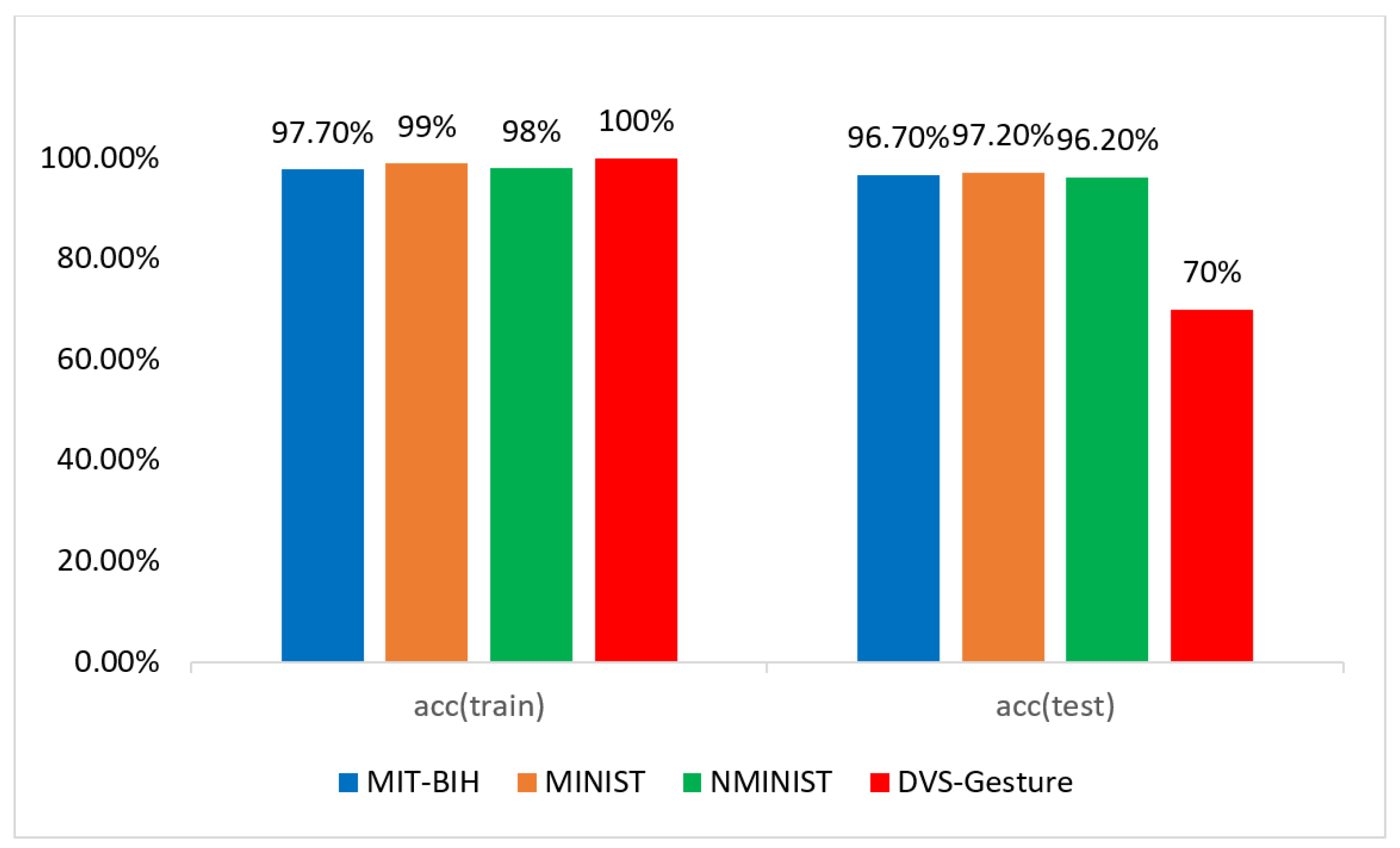
In [22], aiming at the learning dilemmas of Recurrent Spiking Neural Networks (RSNNs)—specifically, RSNNs struggle to achieve complex computational learning through biologically plausible synaptic plasticity rules, while back propagation through time (BPTT), commonly used in traditional machine learning, requires offline storage of intermediate states and time-reversed propagation of signals, which is inconsistent with biological reality—the authors propose an online learning method named e-prop (eligibility propagation). Based on neuroscientific experimental evidence (neuronal eligibility traces and top-down learning signals), mathematical derivation proves that the loss gradient of RSNNs can be decomposed into the sum of products of “local eligibility traces” and “target-specific learning signals”. This method eliminates the need for time-reversed propagation and offline storage in BPTT, enabling biologically plausible online gradient descent learning, and can be extended to supervised learning and deep Reinforcement Learning (RL) scenarios. Meanwhile, authors have introduced the LSNN (LSTM-like spiking neural network) model—composed of Leaky Integrate-and-Fire (LIF) neurons and Adaptive LIF (ALIF) neurons with spike frequency adaptation (SFA)—to improve the computational capability of RSNNs to the level of long short-term memory (LSTM). This enables the algorithm to achieve performance close to that of BPTT with higher energy efficiency. We tested the inference and learning capabilities of the e-prop algorithm across various mainstream applications. As shown in Figure 2, on the MIT-BIH dataset, this learning algorithm achieves a training accuracy of 97.7% and an inference accuracy of 96.7%, which can effectively meet the accuracy requirements of ECG monitoring.
Therefore, this paper adopts the e-prop as on-chip learning algorithm. Due to its improved approximate gradient calculation with low complexity, it is highly hardware-friendly. Combined with the two-layer asynchronous architecture proposed in this paper, the accelerator achieves efficient on-chip learning while maintaining excellent power consumption performance.

3. SNN Processor Overall Design

This section introduces the implementation process of the SNN learning accelerator for ECG monitoring proposed in this paper. This accelerator supports on-chip learning to mitigate the impacts of individual user feature differences. Beyond this, it further adopts a two-layer network architecture and asynchronous data communication to reduce system power consumption.

3.1. Overall Accelerator Design

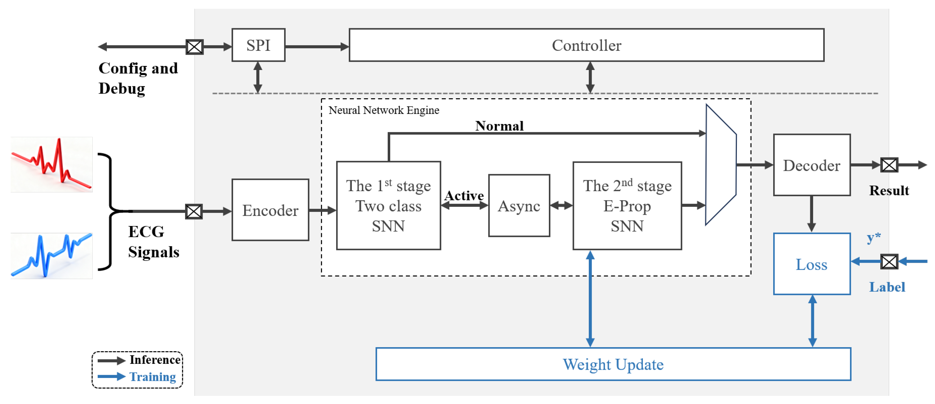
Figure 3 shows the overall system block diagram of the chip. Configuration data is transmitted from the host computer to the chip interior via the SPI interface, received by the Configuration Controller module, and processed for the relevant configuration. The black section at the bottom represents the forward process of the chip: after preliminary processing, ECG data is input into the chip; the encoder is responsible for encoding the input data into spike data that can be processed by the spiking neural network, and then sending the encoded data to the Neural Network Engine (NNE) module for classification. The first-layer network is a two-class lightweight SNN: if the input data is identified as normal ECG, the result is output directly and the operation stops; otherwise, an enable signal is output to activate the second-layer network and input the ECG data into it for abnormal classification. The second-layer network is an e-prop four-class network: upon receiving the enable signal from the first-layer network, this module is activated and classifies the input data into four categories (N, S, V, F) for output. The Neural Network Controller is used to control whether the learning module of the network is enabled. The blue section is the network’s learning module: the loss is calculated using the classified output results and labels; the Weight Update Module performs weight updates and feeds the new weight values back to the network.

3.2. Asynchronous Circuit Technology

In the ECG monitoring scenario, the core requirement of wearable devices is “long battery life”. However, under the traditional synchronous architecture, even if the first-layer binary-classification network detects normal signals (where high-precision classification is unnecessary), the high-precision four-classification network still continues to consume power; this is the primary source of power waste. In contrast, the core advantage of asynchronous circuits lies in the event-driven characteristic: dynamically powering off in the absence of abnormal events and quickly activating when abnormalities occur, which exactly addresses the critical drawback of synchronous architectures.

3.2.1. Asynchronous Communication Design

As shown in Figure 4, the asynchronous communication interface adopts the Click cell as the clock generation component. It only requires using the fire signal generated by the Click cell as the clock for the D flip-flop to complete data transmission. At this point, req_out serves as the valid data signal: when the receiving end successfully samples the signal, it indicates that the received data is valid, and the receiving end then sets ack_out to 1 and feeds it back.
In this paper, we use the active signal of the two classification networks as the input stimulus of the asynchronous communication module. When the fire signal is generated, it transmits abnormal spike data from the first-layer network to the high-precision e-prop SNN network, and simultaneously enables the clock gating module to activate the e-prop SNN network into a working state. When no abnormal data is detected, the high-precision classification network does not consume any dynamic power.

3.2.2. Asynchronous Signal Interaction Based on Click Units

To better illustrate the principle of the asynchronous communication module, the following section describes the working data flow of the Click unit. Figure 5 presents the signal transition diagram of the Click cell. (1) The first stage: when the first-layer binary-classification network detects an abnormal ECG signal, it sends a request input signal (req_in = 1) to the Click unit. At this point, the Click unit immediately generates an activation signal (fire = 1), which serves directly as the clock switch for the high-precision four-classification network, instantly activating the computation modules of the high-precision network. Meanwhile, the Click unit inverts the acknowledge input signal (ack_in) and the request output signal (req_out), notifying the previous stage (the first-layer network) that the request has been received and the subsequent stage (the high-precision network) that it is ready to receive data, respectively. (2) The second stage: After the subsequent high-precision network receives req_out, it feeds back an acknowledge output signal (ack_out = 1). Upon receiving ack_out, the preceding Click unit reactivates the fire signal and inverts ack_in and req_out simultaneously. At this point, req_out serves as a data valid signal, and the spike data of abnormal ECG signals begins to be transmitted from the first-layer network to the high-precision network, completing the data interaction. It can be observed that one event generates two clock signals, enabling data transmission functionality similar to two-phase handshaking.

3.3. Design of SNN Two-Class Network

Since most ECG signals are normal signals, we introduce a two-layer network processing approach. By identifying normal results to stop the network early, system power consumption is reduced. Figure 6 presents the processing flow diagram of the two-class SNN. The first layer uses a lightweight SNN to classify normal and abnormal signals: if the output indicates a normal signal, the network stops early; if the output indicates an abnormal signal, it activates the second-layer e-prop four-class network to perform classification into four categories (N, S, V, F).
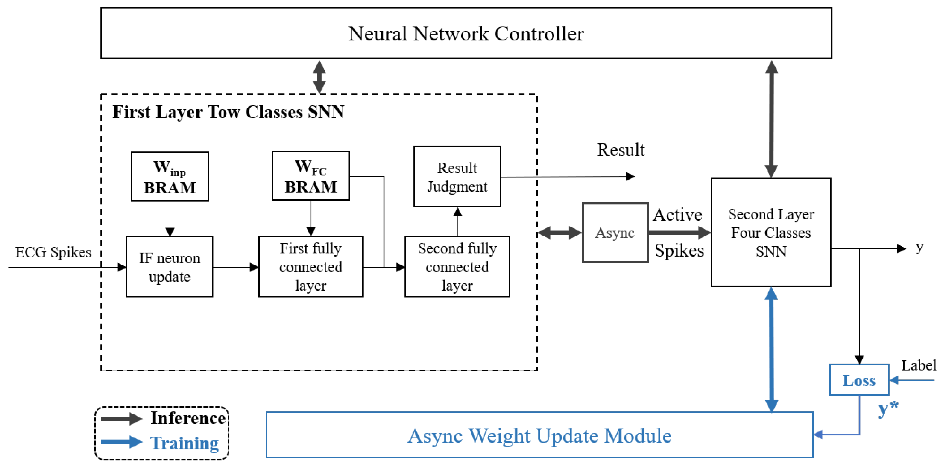
The first-layer network is an extremely simplified custom SNN, designed solely for binary classification judgment. Figure 7 shows the structure diagram of the two-class network. To reduce network resource consumption, Integrate-and-Fire (IF) neurons without a leakage mechanism are adopted in the input layer. External ECG spikes are input into the IF neuron update module, where they accumulate with input weights to compute the membrane potential. After activation, the module outputs spikes, which are processed through two fully connected layers to generate a binary classification result. Based on whether the result indicates an abnormal signal, the system dynamically controls the activation of the high-precision network.
Figure 8 presents the two-layer network classification process. Evaluations indicate that during the binary classification process, the membrane potential data volume is relatively small, so it is stored in a more flexible register-based manner. In a single classification cycle, after external input spikes undergo membrane potential accumulation and activation, a total of 144 spikes are output. These spikes are processed through the first fully connected layer to generate 64 spikes, and then through the second fully connected layer to produce 2 spikes, thereby realizing binary classification.

3.4. Design of Four-Class Network Based on e-Prop Algorithm

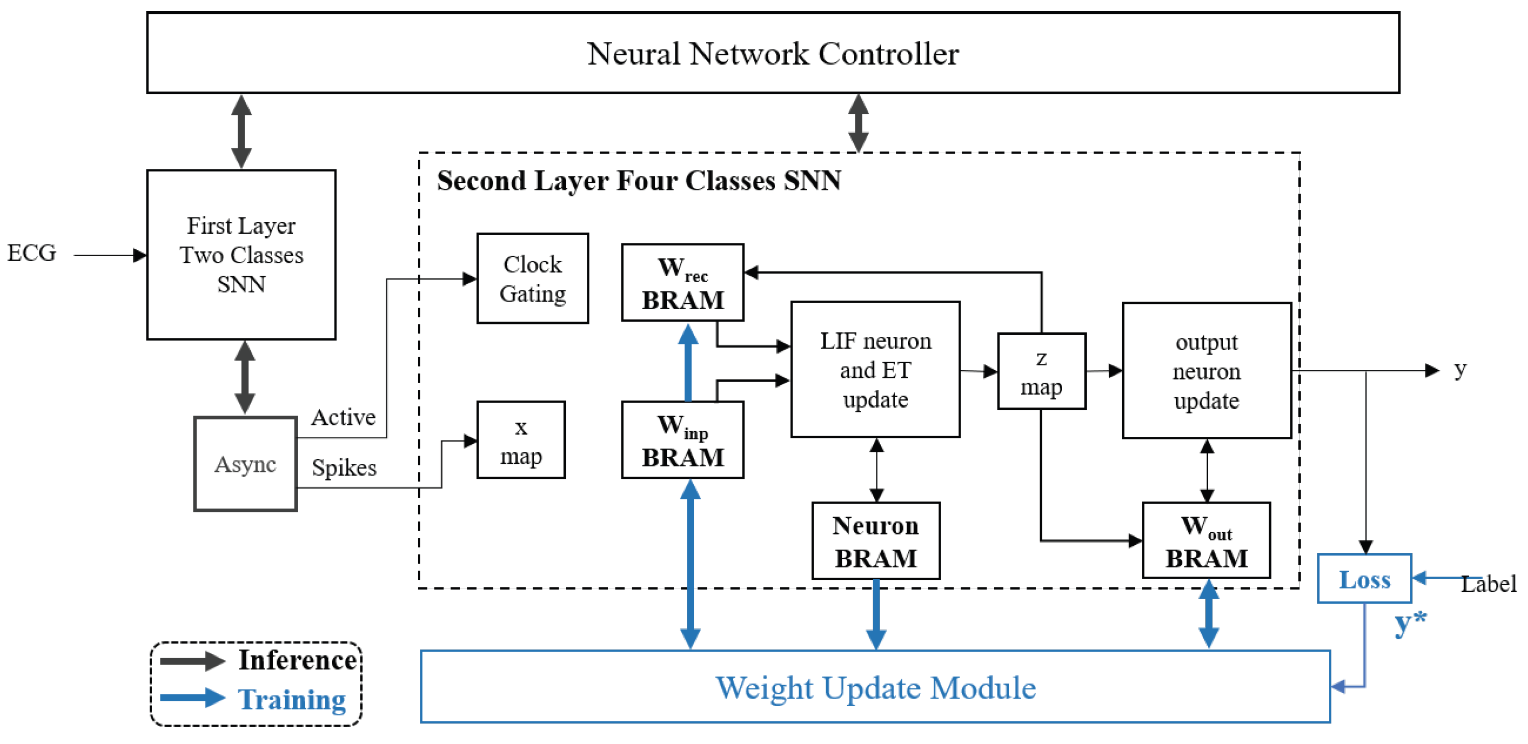
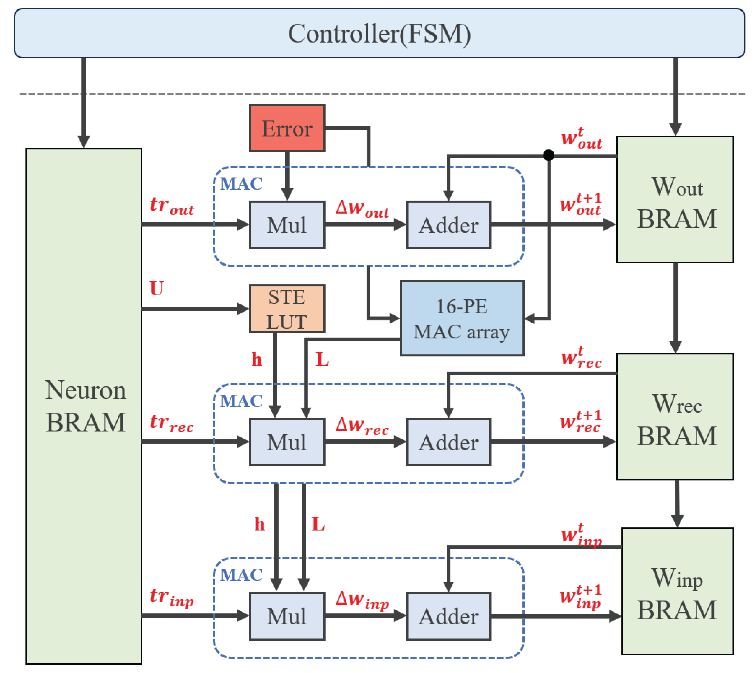
Compared with the classic SNN learning algorithm, back propagation (BP), the e-prop algorithm features lower learning power consumption and better hardware friendliness. Figure 9 shows the structure diagram of the e-prop four-class network. The enable signal from the previous stage activates the operation of this network layer. The first-layer binary-classification network sends the spikes identified as abnormal to the input neurons, and accumulates with the input layer weights to realize membrane potential accumulation. When the membrane potential reaches the firing threshold, the input neurons generate a spike, which serves as the input to the next hidden neurons. Winp BRAM and Wrec BRAM are used to store the weight values of the input and hidden layer neurons, respectively, while Neuron BRAM is used to store neuron information, as well as leakage and threshold parameters. In the output layer, the spike activities of the neurons are aggregated to generate the final output signal; the network converts the output signal into specific task results according to the task type. The blue section is the learning module of this network: if the chip is in the online learning mode, the output results are compared with the target values to generate an error signal, which is then input to the Weight Update Module. The new weight values are fed back to the weight storage BRAMs, completing the weight update process.

3.4.1. Forward Inference Design

The forward path computation of the network mainly includes neuron update and eligibility trace calculation. As shown in Figure 10, the left figure depicts the neuron update process, while the right figure shows the eligibility trace update process. The input and hidden layers adopt LIF neurons, where Equations (1)–(3) represent the update rule of LIF neurons:
v in t + 1 = W in x t ,
v rec t + 1 = W rec z t ,
z t + 1 = H ( v t + 1 v t h ) .
where x t denotes the input spike of the input neuron, which is used for the membrane potential accumulation of the input neuron. At time step t, when the membrane potential reaches the threshold voltage, the input neuron is activated and emits a spike z t , which serves as the input spike of the hidden neuron. Similarly, when the membrane potential of the hidden neuron reaches the threshold voltage, it is activated and emits a spike to the output neuron for the output of the membrane potential value.
The eligibility trace is the core of weight update in the e-prop algorithm. Since the calculation of eligibility traces aligns with the forward path, the computation of eligibility traces is completed simultaneously during the forward process, as shown in Equations (4) and (5):
e j i t = h j t F α ( z i t 1 ) ,
F α ( x t ) = α F α ( x t 1 ) + x t , F α ( x 0 ) = x 0 .
where F α denotes a low-pass filter, and h j t represents the pseudo-derivative z j t v j t of the input spike z j t and membrane potential v j t of the hidden-layer neurons, which is implemented in hardware via a straight-through estimator (STE) LUT lookup. The computed membrane potential values and eligibility trace data are stored in the Neuron BRAM.
In the forward inference design, the state updates of input and hidden layer neurons as well as the calculation of eligibility traces are implemented in the LIF Neuron and ET Update Logic (LNAEUL) module shown in Figure 9, while the inference data is output by the Output Neuron Update Logic (ONUL) module.

3.4.2. Weight Update Design

When the network enables the learning module, the Weight Update Module (WUM) starts to operate. The inference results output by the output neurons are compared with the externally input labels to compute the difference. The weight update algorithm is shown in Equations (6) and (7):
Δ w = d E d W j i = t d E d z j t · d z j t d W j i l o c a l ,
L j t = def k W j k o u t y j t y j , t .
where d z j t d W j i is equivalent to the learning signal L j t , and d E d z j t is equivalent to the eligibility trace signal e j i t . Combining Equations (4), (6) and (7), it can be seen that in the backward learning path, it is only necessary to compute the value of the learning signal and perform a multiply-accumulate operation with the eligibility trace values obtained in the forward pass to obtain the weight update value. After completing the update, the WUM feeds the new weight values back to the corresponding BRAM for storage.
Figure 11 presents the schematic diagram of weight update for the SNN four-class network. The weight update processes for input-layer and hidden-layer neurons are similar: the weights of output layer neurons and the error undergo multiply-accumulate operations to generate the learning signal L; the neuron membrane potential is retrieved via the STE LUT module to obtain the pseudo-derivative h; these two (L and h) are multiplied by the eligibility trace values of input-layer and hidden-layer neurons, respectively, to obtain the updated weights Δ w i n p and Δ w r e c . The weight update of output layer neurons ( Δ w o u t ) is obtained by multiplying the eligibility trace values of the output layer with the error.

4. Experiments and Results

4.1. Experimental Implementation

The hardware platform adopts the xc7z045ffg900 FPGA development board to implement the SNN processor proposed in this paper. The Xilinx XC7Z045-FFG900, developed by Xilinx, a company based in San Jose, CA, USA, is a high-end System-on-Chip (SoC) FPGA in the Zynq-7000 series, which integrates a dual-core ARM Cortex-A9 processor with a maximum operating frequency of 866 MHz and FPGA logic resources. It includes approximately 280 k Look-Up Tables (LUTs), 560 k Flip-Flops (FFs), 192 pieces of 18 Kb Block RAM with a total capacity of 3.456 Mb, and 220 DSP48E1 slices, supporting high-precision arithmetic operations; it is equipped with 4 Phase-Locked Loops (PLLs) and 2 Clock Management Tiles (CMTs), providing flexible clock control; it has 440 configurable I/O pins, supporting various level standards such as LVCMOS and LVDS, and integrates 2 GTP high-speed transceivers with a maximum data rate of 6.5 Gbps, enabling high-speed data transmission.
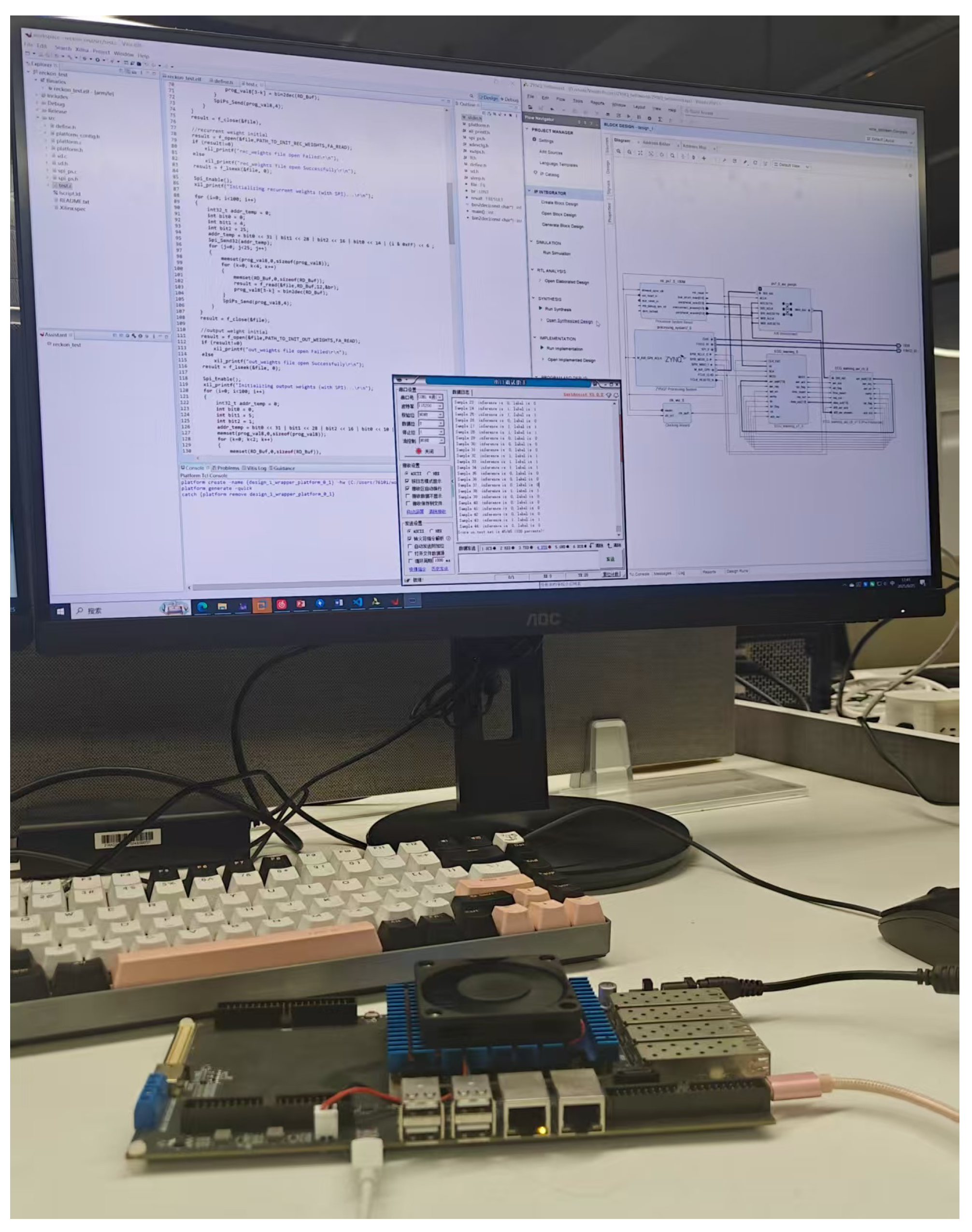
Figure 12 shows the system test environment. The test dataset used for the ECG application is the MIT-BIH dataset.
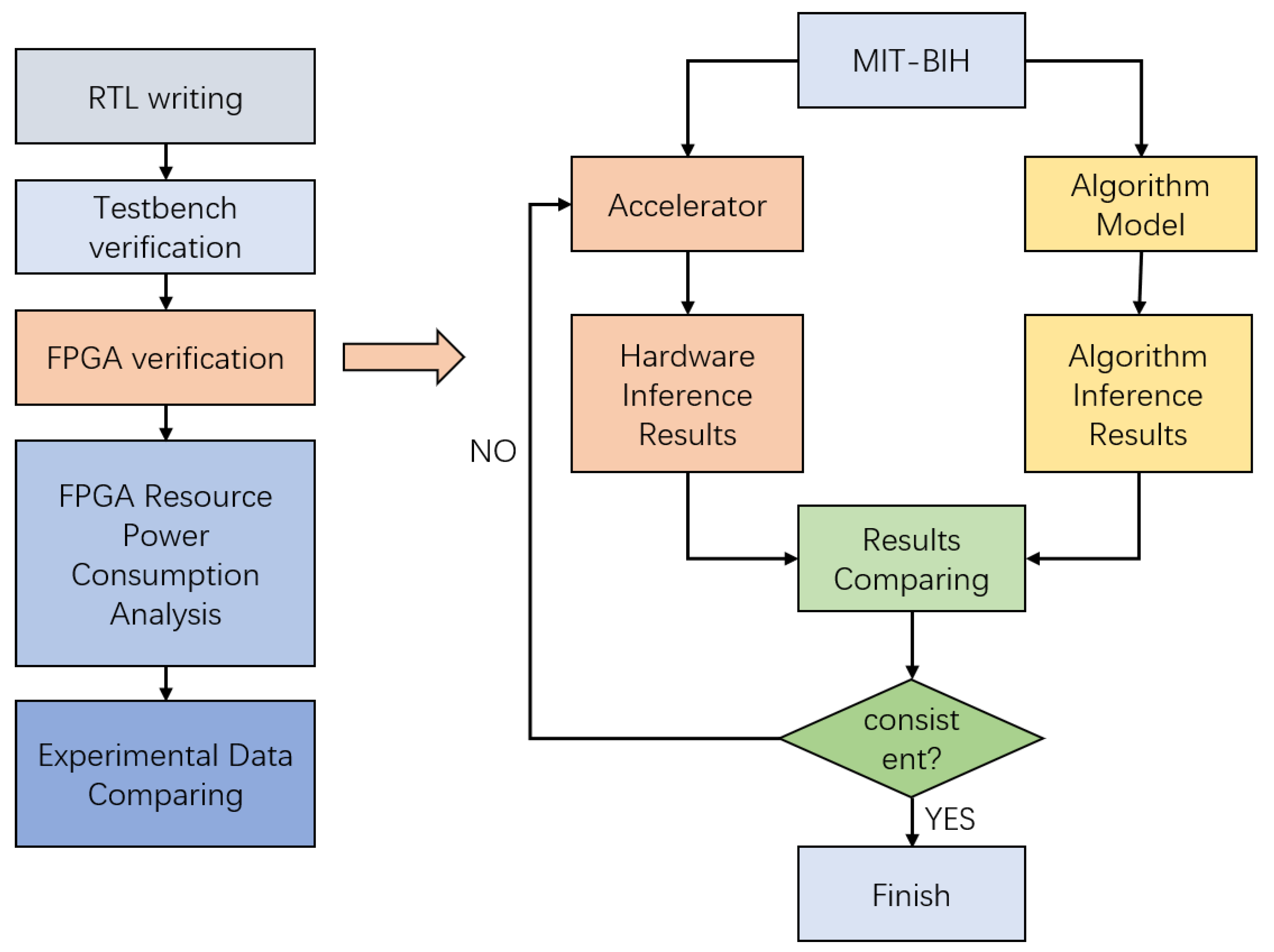
The experimental workflow of this paper is shown on the left side of Figure 13. After completing the initial RTL coding, Testbench functional testing is required for the system to ensure the correctness of RTL functions. Subsequently, placement and routing are performed in Vivado, and a bitstream is generated to prepare for subsequent board-level verification. To ensure the correctness of the accelerator’s functions, functional simulation verification and hardware system verification are conducted respectively. The process of functional simulation verification for this accelerator is shown on the right side of Figure 13: the experimental data required for verification is temporarily stored on the SD card of the FPGA; the on-board ARM core is used as the host computer for data transmission via the SPI interface; meanwhile, the algorithm network on the PC side is used to simulate the operation of the system, and the intermediate values and final inference results are stored in text format. Through text comparison analysis, if all hardware-obtained data (including intermediate data and output results) are completely consistent with those from the algorithm, the hardware and the algorithm can be considered consistent.

4.2. System Design and Module Integration

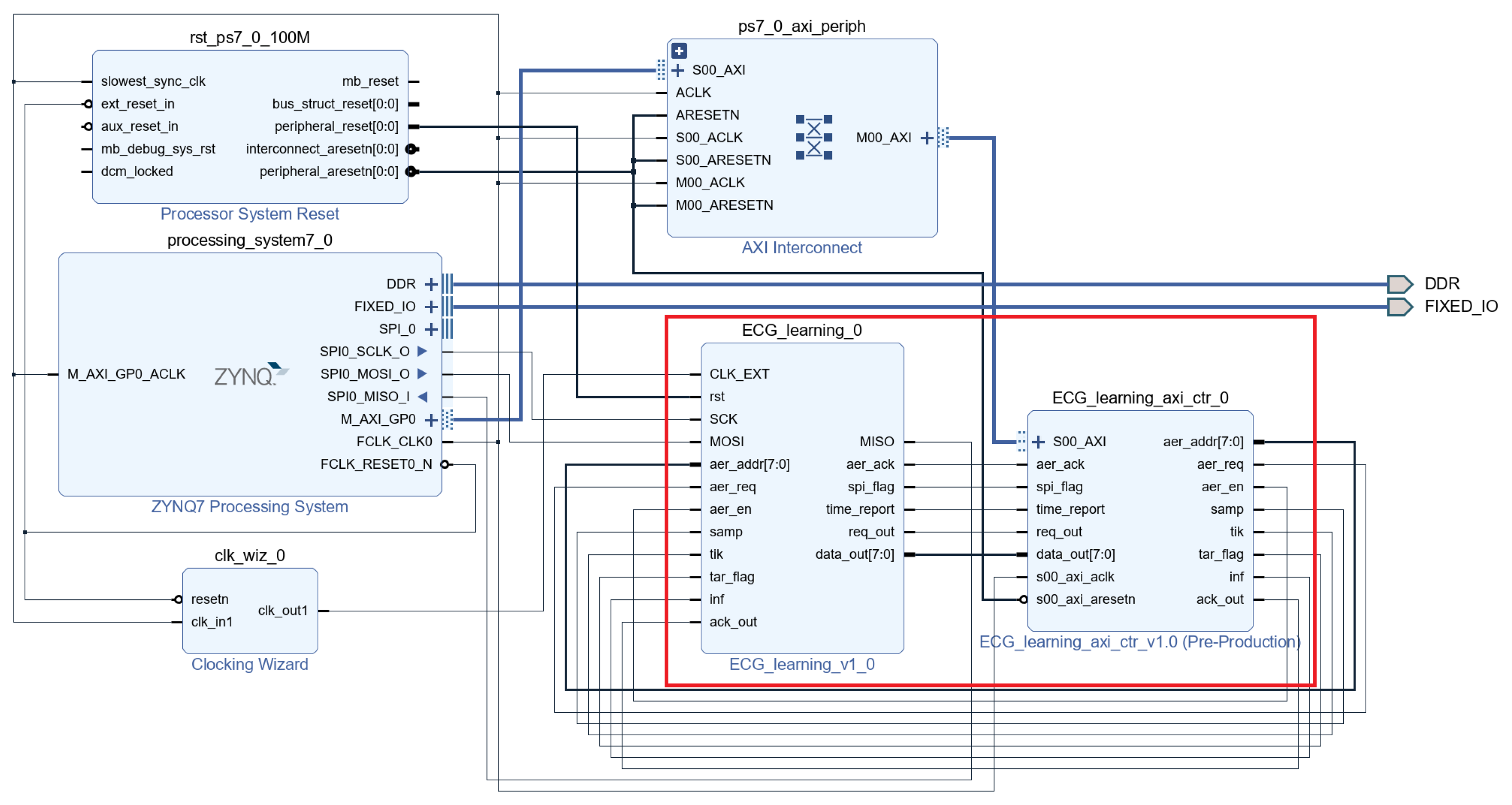
As shown in Figure 14, this paper constructs a system verification platform based on ZYNQ and the AXI bus. The Processing System (PS) side realizes data transmission and reception through the AXI bus, configures the accelerator via the SPI interface, and finally displays the inference or learning results on the host computer through the serial port.
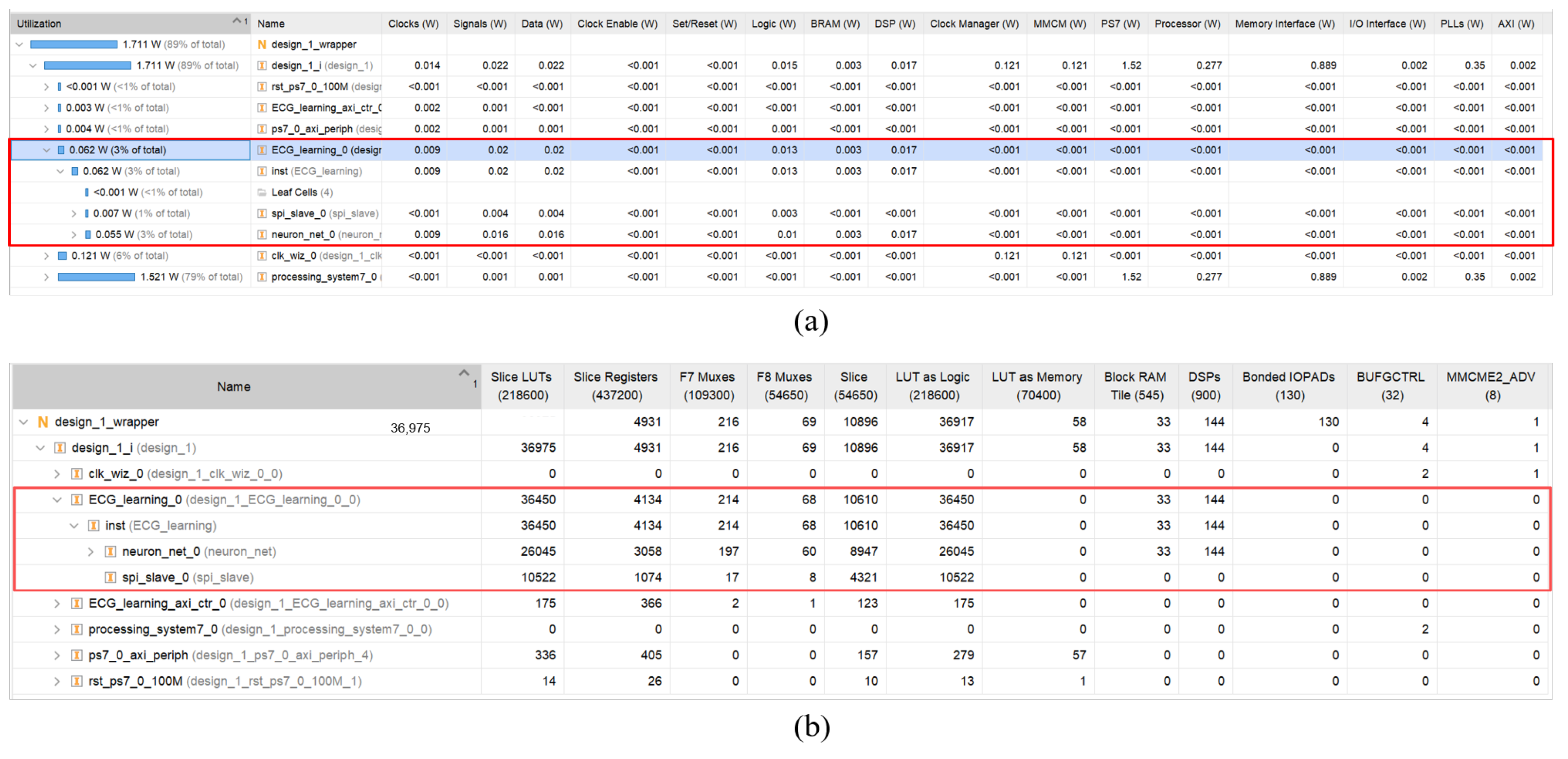
Figure 15 illustrates the resource consumption and power consumption performance of the ECG monitoring-oriented accelerator mentioned in this paper, which is implemented on the xc7z045ffg900 platform.

4.3. Results

4.3.1. First-Stage Inference Evaluation

The two-layer network architecture mentioned in this paper can effectively reduce the overall inference time of the dataset. To verify the effectiveness of the single-layer binary-classification SNN network, an inference experiment on the single-layer network was conducted. The inference results are shown in Figure 16: after 40 epochs, the binary classification accuracy reached 98.6%.

4.3.2. Learning Evaluation

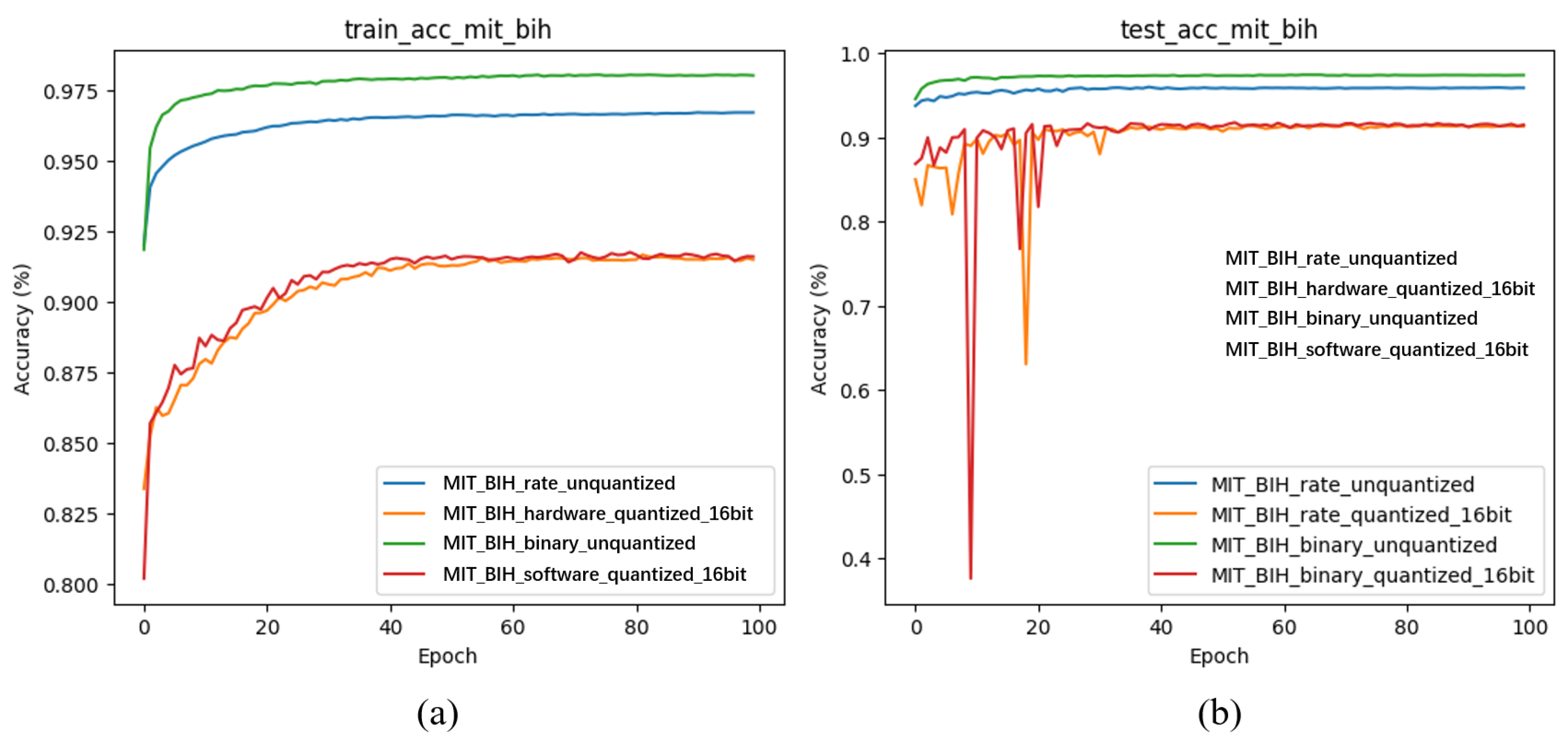
To evaluate the on-chip learning capability and performance of the proposed circuit design, a learning experiment was conducted using the two-layer SNN network adopted in this paper. The experimental results are shown in Figure 17a: the accuracy of the unquantized algorithm is represented by the green and blue curves. After testing, this paper adopted the rate quantization method for design verification, where the results of the quantized algorithm and the hardware test results are presented by the red and orange curves. Before quantization, the training accuracy was 95.8%. To better adapt to hardware implementation, this paper adopts an 8-bit weight and 16-bit membrane potential quantization scheme. Finally, the post-quantization training accuracy reaches 91.4%, representing a reduction of 4.4%.

4.3.3. Overall Inference Evaluation

To evaluate the inference performance of the designed processor, an inference experiment was conducted using the two-layer SNN network adopted in this paper. Consistent with other state-of-the-art works targeting ECG applications, 73,753 samples from the MIT-BIH training dataset were used for training, and 18,439 samples from the MIT-BIH test dataset were employed for testing. The average classification time per ECG data sample was 3.48 ms. As shown in Figure 17b, the tested classification accuracy reached 91.4%, which is basically consistent with the training results. To verify the effectiveness of the proposed two-layer design, we further tested the classification time and power of a design that only uses a single e-prop network. The results are presented in Table 1. By conducting four-classification inference experiments on the single-layer e-prop network and the two-layer SNN network, with a consistent sample size of 18,439 for both experiments, the results show that the single e-prop network consumed 188,815 ms, while the two-layer SNN network took 64,099 ms. After calculation, the single classification time of the two networks is 10.24 ms and 3.48 ms, respectively, and the energy consumption per classification is 481.28 μ J and 215.53 μ J , indicating that the classification time and energy consumption are reduced by 66.1% and 55.2%, respectively.

4.3.4. Comparison with Other Chips

Table 2 compares the proposed design with state-of-the-art SNN processors, including information such as computation time for inference, on-chip learning, target applications, energy consumption, and classification accuracy. For a fair comparison of the performance of applications with different scales and types, normalization was performed, and the energy consumption per classification was calculated independently. It can be seen from the table that for inference, the designed processor achieves relatively higher energy efficiency (215.53 μ J per classification) and faster computation time (3.48 ms), while reaching a binary-classification accuracy of 98.6%, and a four-classification accuracy of 91.4% for ECG detection. For learning, most ECG chips do not support this function; compared with Xing et al. [23], the proposed design achieves 91.4% classification accuracy while exhibiting higher energy efficiency (215.53 μ J ).
Considering the reasonable trade-off between low-power constraints, model complexity, and computational resource allocation, this design inevitably makes a moderate compromise in model expressiveness to pursue low power consumption that meets the long battery life requirement of ECG monitoring. However, this accuracy is still compatible with the intended application scenario. Furthermore, this paper processes the classification accuracy and energy efficiency data to obtain the accuracy–energy efficiency ratio. As shown in Figure 18, the proposed accelerator achieves a good balance between accuracy and power consumption. Moreover, the core requirement of ECG monitoring is the early identification of abnormal signals to support timely intervention. The 98.6% binary-classification accuracy of the first layer in this design can already efficiently screen normal signals, and the classification accuracy of the high-precision four-classification module for abnormal signals is sufficient to meet the needs of daily health monitoring.

5. Conclusions

In this work, we present an FPGA-based SNN learning chip for ECG monitoring implemented on a Xilinx XC7Z045. Through the hardware implementation of the e-prop algorithm, efficient on-chip learning is achieved, which effectively mitigates the impacts of individual user feature differences. Meanwhile, a two-layer dynamic neural network architecture and asynchronous data transmission between modules are adopted to further reduce system power consumption. The proposed design achieves an accuracy of 98.6% for the first-layer binary classification network and 91.4% for the second-layer four-class classification network at 25 MHz, with an energy consumption of 0.062 W and 215.53 μ J per classification. These characteristics provide a new approach for wearable medical devices in environments constrained by power consumption and accuracy requirements.
Future work will extend beyond enhancing abnormal monitoring accuracy and supporting more biomedical signals to three key directions: First, clinical trials will be conducted with medical institutions to verify the chip’s performance in real-world scenarios and align it with medical device regulatory standards. Second, patient-specific adaptation will be advanced by integrating long-term physiological data to dynamically refine model parameters, adapting to changes in a patient’s cardiovascular status over time. Third, IoT healthcare system integration will be realized, connecting the chip to wearable ecosystems and hospital information systems for real-time remote monitoring, with a focus on medical data security and privacy protection. These extensions aim to bridge laboratory prototypes and clinical applications, advancing patient-centric cardiovascular care.

Author Contributions

Conceptualization, J.M.; methodology, J.M.; software, F.S.; validation, J.M.; formal analysis, J.M.; investigation, J.M. and Y.H.; resources, J.M. and Y.H.; data curation, J.M. and F.S.; writing—original draft preparation, J.M.; writing—review and editing, Y.L., Y.H., and D.M.; visualization, J.M.; supervision, Y.H. and D.M.; project administration, D.M.; funding acquisition, D.M. All authors have read and agreed to the published version of the manuscript.

Funding

This work was supported by the National Key Research and Development Program of China under Grant 2020AAA0109002, the grants from the Key R&D Program of Zhejiang under Grant 2022C01048, and the Key Program of the National Natural Science Foundation of China under Grant 62334014.

Data Availability Statement

The data are available on request to the corresponding authors.

Conflicts of Interest

The authors declare no conflicts of interest. The funders had no role in the design of the study; in the collection, analyses, or interpretation of data; in the writing of the manuscript; or in the decision to publish the results.

References

  1. Xiang, Z.; Han, M.; Zhang, H. Nanomaterials based flexible devices for monitoring and treatment of cardiovascular diseases (CVDs). Nano Res. 2023, 16, 3939–3955. [Google Scholar] [CrossRef]
  2. Ieong, C.I.; Mak, P.I.; Lam, C.P.; Dong, C.; Vai, M.I.; Mak, P.U.; Pun, S.H.; Wan, F.; Martins, R.P. A 0.83-μW QRS Detection Processor Using Quadratic Spline Wavelet Transform for Wireless ECG Acquisition in 0.35- μm CMOS. IEEE Trans. Biomed. Circuits Syst. 2012, 6, 586–595. [Google Scholar] [CrossRef] [PubMed]
  3. Kumar, N.; Raj, S. An Adaptive Scheme for Real-Time Detection of Patient-Specific Arrhythmias Using Single-Channel Wearable ECG Sensor. IEEE Sens. Lett. 2024, 8, 1–4. [Google Scholar] [CrossRef]
  4. Boumaiz, M.; Ghazi, M.E.; Bouayad, A.; Balboul, Y.; El Bekkali, M. Energy-Efficient Strategies in Wireless Body Area Networks: A Comprehensive Survey. IoT 2025, 6, 49. [Google Scholar] [CrossRef]
  5. Cai, W.; Hu, D. QRS Complex Detection Using Novel Deep Learning Neural Networks. IEEE Access 2020, 8, 97082–97089. [Google Scholar] [CrossRef]
  6. Zhang, Z.; Guan, Y.; Ye, W. An Energy-Efficient ECG Processor with Ultra-Low-Parameter Multistage Neural Network and Optimized Power-of-Two Quantization. IEEE Trans. Biomed. Circuits Syst. 2024, 18, 1296–1307. [Google Scholar] [CrossRef] [PubMed]
  7. Buzura, S.; Iancu, B.; Dadarlat, V.; Peculea, A.; Cebuc, E. Optimizations for Energy Efficiency in Software-Defined Wireless Sensor Networks. Sensors 2020, 20, 4779. [Google Scholar] [CrossRef] [PubMed]
  8. Lu, J.; Liu, D.; Cheng, X.; Wei, L.; Hu, A.; Zou, X. An Efficient Unstructured Sparse Convolutional Neural Network Accelerator for Wearable ECG Classification Device. IEEE Trans. Circuits Syst. Regul. Pap. 2022, 69, 4572–4582. [Google Scholar] [CrossRef]
  9. Mao, R.; Li, S.; Zhang, Z.; Xia, Z.; Xiao, J.; Zhu, Z.; Liu, J.; Shan, W.; Chang, L.; Zhou, J. An Ultra-Energy-Efficient and High Accuracy ECG Classification Processor with SNN Inference Assisted by On-Chip ANN Learning. IEEE Trans. Biomed. Circuits Syst. 2022, 16, 832–841. [Google Scholar] [CrossRef] [PubMed]
  10. Zhang, J.; Liang, M.; Wei, J.; Wei, S.; Chen, H. A 28 nm Configurable Asynchronous SNN Accelerator with Energy-Efficient Learning. In Proceedings of the 2021 27th IEEE International Symposium on Asynchronous Circuits and Systems (ASYNC), Beijing, China, 7–10 September 2021; pp. 34–39. [Google Scholar] [CrossRef]
  11. Zhang, J.; Wang, R.; Pei, X.; Luo, D.; Hussain, S.; Zhang, G. A Fast Spiking Neural Network Accelerator based on BP-STDP Algorithm and Weighted Neuron Model. IEEE Trans. Circuits Syst. II Express Briefs 2022, 69, 2271–2275. [Google Scholar] [CrossRef]
  12. Liu, J.; Xiao, J.; Fan, J.; Liu, Q.; Zhu, Z.; Li, S.; Zhang, Z.; Yang, S.; Shan, W.; Lin, S.; et al. An Energy-Efficient Cardiac Arrhythmia Classification Processor using Heartbeat Difference based Classification and Event-Driven Neural Network Computation with Adaptive Wake-Up. In Proceedings of the 2022 IEEE Custom Integrated Circuits Conference (CICC), Newport Beach, CA, USA, 24–27 April 2022; pp. 1–2. [Google Scholar] [CrossRef]
  13. Ku, M.Y.; Zhong, T.S.; Hsieh, Y.T.; Lee, S.Y.; Chen, J.Y. A High Performance Accelerating CNN Inference on FPGA with Arrhythmia Classification. In Proceedings of the 2023 IEEE 5th International Conference on Artificial Intelligence Circuits and Systems (AICAS), Hangzhou, China, 11–13 June 2023; IEEE: New York, NY, USA, 2023; pp. 1–4. [Google Scholar]
  14. Lu, J.; Liu, D.; Liu, Z.; Cheng, X.; Wei, L.; Zhang, C.; Zou, X.; Liu, B. Efficient Hardware Architecture of Convolutional Neural Network for ECG Classification in Wearable Healthcare Device. IEEE Trans. Circuits Syst. I (TCASI) 2021, 68, 2976–2985. [Google Scholar] [CrossRef]
  15. Zhang, J.; Wang, Y.; Cai, Y.; Bi, B.; Chen, Q.; Zhang, Y. A Low Power Spiking Neural Network Accelerator on FPGA for Real-Time Edge Computing. In Proceedings of the International Symposium on Autonomous Systems (ISAS), Xi’an, China, 23–25 May 2025; pp. 1–6. [Google Scholar] [CrossRef]
  16. Yu, A.; Ahmadi, A.; MacEachern, L. Low-Cost Spiking Networks on FPGA for Event-Based Gesture Detection. In Proceedings of the 2025 International Symposium on Signals, Circuits and Systems (ISSCS), Iasi, Romania, 17–18 July 2025; pp. 1–4. [Google Scholar] [CrossRef]
  17. Mangaraj, S.; Oraon, P.; Ari, S.; Swain, A.K.; Mahapatra, K. FPGA Accelerated Convolutional Neural Network for Detection of Cardiac Arrhythmia. In Proceedings of the 4th IEEE International Conference on VLSI Systems, Architecture, Technology and Applications (VLSI SATA), Bengaluru, India, 17–18 May 2024; IEEE: New York, NY, USA, 2024; pp. 1–6. [Google Scholar]
  18. Rawal, V.; Prajapati, P.; Darji, A. Hardware implementation of 1D-CNN architecture for ECG arrhythmia classification. Biomed. Signal Process. Control 2023, 85, 104865. [Google Scholar] [CrossRef]
  19. Jameil, A.K.; Al-Raweshidy, H. Efficient CNN Architecture on FPGA Using High Level Module for Healthcare Devices. IEEE Access 2022, 10, 60486–60495. [Google Scholar] [CrossRef]
  20. Aamir, S.A.; Müller, P.; Kiene, G.; Kriener, L.; Stradmann, Y.; Grübl, A.; Schemmel, J.; Meier, K. A Mixed-Signal Structured AdEx Neuron for Accelerated Neuromorphic Cores. IEEE Trans. Biomed. Circuits Syst. 2018, 12, 1027–1037. [Google Scholar] [CrossRef] [PubMed]
  21. Zhang, J.; Wu, H.; Wei, J.; Wei, S.; Chen, H. An Asynchronous Reconfigurable SNN Accelerator With Event-Driven Time Step Update. In Proceedings of the 2019 IEEE Asian Solid-State Circuits Conference (A-SSCC), Macao, China, 4–6 November 2019; pp. 213–216. [Google Scholar] [CrossRef]
  22. Juarez-Lora, A.; Ponce-Ponce, V.H.; Sossa, H.; Rubio-Espino, E. R-STDP Spiking Neural Network Architecture for Motion Control on a Changing Friction Joint Robotic Arm. Front. Neurorobot. 2022, 16, 904017. [Google Scholar] [CrossRef] [PubMed]
  23. Xing, Y.; Zhang, L.; Hou, Z.; Li, X.; Shi, Y.; Yuan, Y.; Zhang, F.; Liang, S.; Li, Z.; Yan, L. Accurate ECG Classification Based on Spiking Neural Network and Attentional Mechanism for Real-Time Implementation on Personal Portable Devices. Electronics 2022, 11, 1889. [Google Scholar] [CrossRef]
  24. Liu, Y.; Dong, L.; Zhang, B.; Xin, Y.; Geng, L. Real Time ECG Classification System Based on DWT and SVM. In Proceedings of the 2020 IEEE International Conference on Integrated Circuits, Technologies and Applications (ICTA), Nanjing, China, 23–25 November 2020; IEEE: New York, NY, USA, 2020; pp. 155–156. [Google Scholar]
  25. Liu, Y.; Wang, Z.; He, W.; Shen, L.; Zhang, Y.; Chen, P.; Wu, M.; Zhang, H.; Zhou, P.; Liu, J.; et al. An 82 nW 0.53 pJ/SOP Clock-Free Spiking Neural Network with 40 µs Latency for AloT Wake-Up Functions Using Ultimate-Event-Driven Bionic Architecture and Computing-in-Memory Technique. In Proceedings of the 2022 IEEE International Solid-State Circuits Conference (ISSCC), San Francisco, CA, USA, 20–26 February 2022; Volume 65, pp. 372–374. [Google Scholar] [CrossRef]
  26. Janveja, M.; Parmar, R.; Tantuway, M.; Trivedi, G. A DNN-Based Low Power ECG Co-Processor Architecture to Classify Cardiac Arrhythmia for Wearable Devices. IEEE Trans. Circuits Syst. II Express Briefs 2022, 69, 2281–2285. [Google Scholar] [CrossRef]
  27. Rana, A.; Kim, K.K. Comparison of Artificial Neural Networks for Low-Power ECG-Classification System. Senseo Haghoeji 2020, 29, 19–26. [Google Scholar] [CrossRef]
  28. Liu, Z.; Ling, X.; Zhu, Y.; Wang, N. FPGA-based 1D-CNN accelerator for real-time arrhythmia classification. J.-Real-Time Image Process. 2025, 22, 66. [Google Scholar] [CrossRef]

Figure 1. Cardiovascular disease mortality rate.
Electronics 14 04923 g001
Figure 2. Accuracy of e-prop.
Electronics 14 04923 g002
Figure 3. System block diagram. The black sections represent the forward inference process, and the blue sections represent the learning process.
Electronics 14 04923 g003
Figure 4. Asynchronous communication interface.
Electronics 14 04923 g004
Figure 5. The signal transition diagram of Click.
Electronics 14 04923 g005
Figure 6. Two-layer network processing.
Electronics 14 04923 g006
Figure 7. Structure diagram of the two-class network. The black sections represent the forward inference process, and the blue sections represent the learning process.
Electronics 14 04923 g007
Figure 8. Two-layer network classification process.
Electronics 14 04923 g008
Figure 9. Structure diagram of the e-prop four-class network. The black sections represent the forward inference process, and the blue sections represent the learning process.
Electronics 14 04923 g009
Figure 10. Forward inference design: (a) neuron update process and (b) eligibility trace update process.
Electronics 14 04923 g010
Figure 11. Weight update.
Electronics 14 04923 g011
Figure 12. System test environment.
Electronics 14 04923 g012
Figure 13. Experimental workflow.
Electronics 14 04923 g013
Figure 14. FPGA block design. The content within the box is the module design of the accelerator on FPGA.
Electronics 14 04923 g014
Figure 15. Hardware analysis of the system design: (a) power consumption and (b) resource utilization. The contents within the box are the power consumption and resource utilization of the accelerator on FPGA.
Electronics 14 04923 g015
Figure 16. First-stage inference accuracy over epochs.
Electronics 14 04923 g016
Figure 17. Accuracy results: (a) train result of 100 epochs and (b) test result of 100 epochs.
Electronics 14 04923 g017
Figure 18. Accuracy–energy efficiency ratio. Mangaraj 2024 [17], Liu 2020 [24], Xing 2022 [23], Rana 2020 [27], Liu 2025 [28].
Electronics 14 04923 g018
Table 1. Comparison between single- and two-layer network.
Single e-Prop NetworkTwo-Layer SNN Network
Total Classification Time (ms)188,81564,099
Sample Size18,43918,439
Average Classification Time (ms)10.243.48
Power (W)0.0470.062
Energy/Classification ( μ J )481.28215.53
Accuracy (%)91.791.4
Table 2. Comparison with the ECG processor.
[17][24][23][25]
DeviceZCU 104XC7Z020Artix-7180 nm ASIC
MethodsCNNSVMSNNSNN
DatasetMIT-BIHMIT-BIHMIT-BIHMIT-BIH
Clock (MHz)---Asynchronous
Accuracy (%)98.64%98.7%92.07%90.5%
Classification Time (ms)2190.281.32-
Power (W)4.1772.0590.2460.35  μ
Energy/Classification ( μ J )914,763576.52324.72-
On-chip LearningNONONONO
[26][27][28]This Work
Device180 nm ASICXC7Z020Zynq-XC7Z020XC7Z045
MethodsDNNCNNCNNSNN
DatasetMIT-BIHMIT-BIHMIT-BIHMIT-BIH
Clock (Hz)12 K-50 M25 M
Accuracy (%)91.6%95%96.55%98.6%/91.4% *
Classification Time (ms)-791.6633.48
Power (W)8.75  μ 2.2661.780.062
Energy/Classification ( μ J )2.081,793,766112,140215.53
On-chip LearningNONONOYES
* Note: 98.6% corresponds to the binary-classification accuracy at the preprocessing stage, and 91.4% represents the high-precision four-classification accuracy.
Disclaimer/Publisher’s Note: The statements, opinions and data contained in all publications are solely those of the individual author(s) and contributor(s) and not of MDPI and/or the editor(s). MDPI and/or the editor(s) disclaim responsibility for any injury to people or property resulting from any ideas, methods, instructions or products referred to in the content.