1. Introduction
At the critical juncture of the global energy transition toward cleanliness and low carbon, photovoltaic (PV) energy storage systems have become the core carrier for renewable energy integration, with their operational safety and power quality directly affecting grid stability [
1]. Medium-to-high voltage PV energy storage applications (such as commercial and industrial energy storage, microgrids) impose an urgent demand for inverters with “high voltage withstand capability, low losses, and resistance to three-phase imbalance.” Benefiting from the significant advantages of multilevel topology in reducing switching voltage stress and the fourth arm in mitigating load imbalance, non-isolated three-level four-leg inverters have emerged as the mainstream solution in this field [
2]. However, this topology has inherent flaws: the parasitic capacitance between the PV array and the ground (typical value: 50–150 nF/kW [
3]) forms leakage current paths under high-frequency common-mode voltage excitation; furthermore, fluctuations in the DC-side neutral point potential induced by four-leg control further amplify the common-mode loop gain, resulting in peak leakage current of the traditional topology far exceeding the 300 mA limit specified in China’s NB/T 32004-2018 [
4] and GB/T 20321-2023 [
5] standards. This not only causes additional power losses and impairs grid power quality but also accelerates equipment insulation aging, posing a threat to personnel safety.
To address the leakage current challenge, the academic community has developed two primary technical approaches, “control optimization” and “topology improvement,” both of which have significant limitations. At the control strategy level, reference [
6] adopts unipolar SPWM technology to maintain a constant common-mode voltage (Vdc/2) and eliminates additional leakage current paths through freewheeling mode, achieving low leakage current RMS values of 11.09 mA (H9 topology)/11.73 mA (H10 topology). However, this scheme is only applicable to single-phase low-voltage systems, and the H10 topology incorporates 10 switching devices, resulting in high costs; reference [
7] employs non-high-frequency-jump space vectors, realizing a leakage current RMS ≤ 4.95 mA that is independent of switching frequency and input voltage, with 60% of the power transmitted directly to improve efficiency. Nevertheless, it only has 19 effective space vectors, leading to high control complexity and requiring two additional inductors, which increases volume and cost; reference [
8] proposes an optimized Discrete Pulse Width Modulation (DPWM) strategy that can reduce leakage current under unbalanced midpoint voltage conditions of three-level inverters, but it necessitates real-time adjustment of switching sequences, imposing stringent requirements on controller computing power; reference [
9] designs an integrated modulation strategy for dual-parallel three-level inverters to suppress leakage current by coordinating the switching states of bridge arms, yet this scheme is only suitable for specific parallel topologies and lacks universality; reference [
10] presents a leakage current suppression modulation scheme for split capacitor four-wire current-source inverters, which can reduce leakage current but fails to adapt to the charge–discharge characteristics of photovoltaic energy storage systems; reference [
11] proposes a leakage current suppression scheme (optimized SVPWM with synchronous switching points to eliminate the 2Vdc/3 common-mode voltage), which requires no additional hardware and achieves significant suppression (especially at low speeds) without compromising control performance. However, it results in a slight increase in current harmonics, limited gain at high speeds, and relies on switching synchronization.
At the topology improvement level, most existing solutions achieve leakage current suppression at the cost of increasing the number of components: Reference [
12] proposes a leakage current suppression scheme combining the H8 topology, dedicated modulation, and SiC devices. This scheme features accurate common-mode voltage control, compatibility with SiC devices for optimized lifespan, and high strategy flexibility. However, the CCMV-SV (Common-Mode Voltage Suppression Space Vector) is limited by the modulation index, additional components increase losses, SiC devices entail high costs, and extra filtering is required to suppress second harmonic components. Reference [
13] presents a five-level inverter topology that reduces the leakage current RMS to 13.82 mA by stabilizing the common-mode voltage, but it requires 11 switching devices, leading to a more than 20% increase in conduction losses; reference [
14] adopts a switched-capacitor impedance source structure, which enhances voltage gain while suppressing leakage current. Its four-leg configuration can adapt to three-phase unbalanced loads and reduces common-mode voltage transients, yet the charging and discharging of switched capacitors may introduce high-frequency leakage current components, necessitating additional capacitors/inductors and increasing the topology volume; reference [
15] uses four miniature film capacitors to achieve open-circuit and short-circuit immunity, minimize switching overlap time, and naturally balance inductor currents, thereby reducing leakage current sources. However, it is only applicable to current-source inverters, requires additional capacitors leading to higher costs, and has limited application scenarios; reference [
16] designs a seven-level transformerless grid-connected inverter integrating boost and leakage current-limiting functions, achieving negligible peak leakage current. Nevertheless, it needs four additional capacitors and two diodes to construct the switched-capacitor unit, resulting in high topological complexity and a 35% cost increase; reference [
17] adopts an input–output common-ground design to eliminate leakage current paths, with a unidirectional active buffer circuit isolating ripple power without electrolytic capacitors, improving long-term stability. However, this scheme is only suitable for single-phase systems, requires high-voltage-rated buffer capacitors, and may exhibit reduced leakage current suppression performance when scaled to three-phase topologies; reference [
18] proposes a switched-boost four-leg inverter that maintains constant common-mode voltage using the fourth leg, enabling leakage current control at 18.4 mA. However, the DC side requires two inductors and one capacitor, which is unfavorable for system miniaturization; reference [
19] designs a five-level transformerless topology based on capacitive voltage division that can completely eliminate leakage current, but it needs an additional inductor to limit capacitor charging current, reducing dynamic response speed; reference [
20] only adds one diode, achieving complete leakage current elimination (RMS ≤ 0.7 mA) at low PV voltages and a 90% leakage current reduction at high voltages with only a 0.3% efficiency drop. However, when the PV voltage exceeds 480 V, the leakage current suppression effectiveness decreases to 50%, requiring coordinated control with boost and inverter switches; reference [
21] presents a HERIC cascaded H-bridge inverter that suppresses leakage current through AC-side decoupling, but the cascaded structure increases control degrees of freedom, complicating neutral point potential balancing; reference [
22] proposes a coupled inductor functional expansion damping scheme, embedding damping windings in parallel inverters to suppress common-mode leakage current. However, it requires redesigning the inductor structure, posing significant challenges for engineering implementation.
Furthermore, there exists a significant research gap in dedicated topologies for photovoltaic (PV) energy storage scenarios. Most existing solutions focus on grid-connected inverters, neglecting the coupling impact of DC-side voltage fluctuations on leakage current during the charge–discharge switching of energy storage systems. Common-ground topologies [
23] eliminate common-mode voltage fluctuations through direct grounding, achieving excellent leakage current suppression performance. However, they are not suitable for floating PV systems or multi-string energy storage systems; boost–buck topologies [
24] can adapt to low PV input voltages but often overlook the coupling relationship between leakage current and neutral point potential balancing. Although the nine-level transformerless boost inverter proposed in the reference significantly reduces leakage current, it requires complex fractional power transfer control, posing substantial challenges for engineering implementation; reference [
25] presents a hybrid energy storage scheme combined with a ten-switch inverter, which improves power quality but lacks optimization for leakage current issues, resulting in limited applicability.
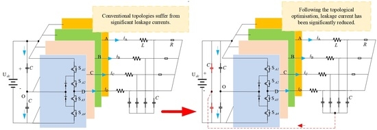
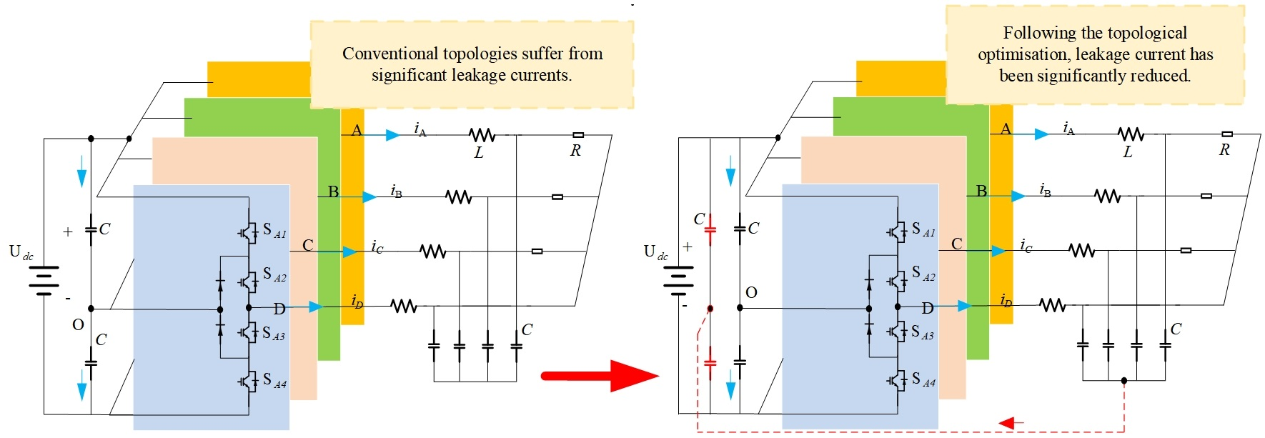
To address the aforementioned challenges, this paper focuses on the topological optimization of a four-leg photovoltaic (PV) energy storage inverter, aiming to achieve the goal of “high operational adaptability with minimal component increments without relying on additional complex control.” Based on Kirchhoff’s laws, a common-mode equivalent circuit of the traditional three-level four-leg topology is established, the leakage current expression is derived, and the coupling mechanism of parasitic capacitance, filter inductance, and neutral point potential fluctuations on leakage current is quantitatively analyzed. This study systematically reveals the common flaws of existing solutions: control strategies rely on complex algorithms, topology improvements sacrifice cost and efficiency, and dedicated topologies have poor adaptability. An improved topology based on independent voltage-divider capacitors is proposed. This scheme only adds two independent voltage-divider capacitors (with capacitance much smaller than the main capacitors) on the DC side and connects the midpoint of the output filter capacitors to the midpoint of the voltage-divider capacitors. This design simultaneously constructs an active discharge path for common-mode current and avoids modulation failure that may be caused by direct grounding of the DC-side neutral point. Simulation and experimental verifications demonstrate the excellent performance of the improved topology in leakage current suppression.
The remainder of this paper is structured as follows:
Section 2 establishes the common-mode model of the traditional topology and analyzes the leakage current mechanism;
Section 3 elaborates on the proposed improved topology and its operating principle in detail;
Section 4 verifies the effectiveness and superiority of the proposed topology through comparative simulations and experiments;
Section 5 summarizes the entire paper.
2. Traditional Three-Level Three-Phase Four-Leg Photovoltaic Energy Storage Inverter Topology
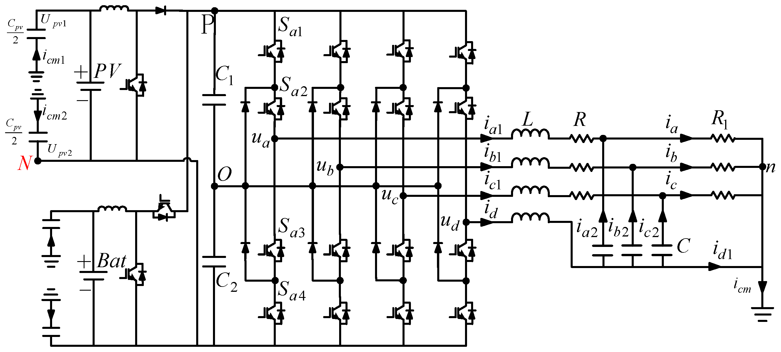
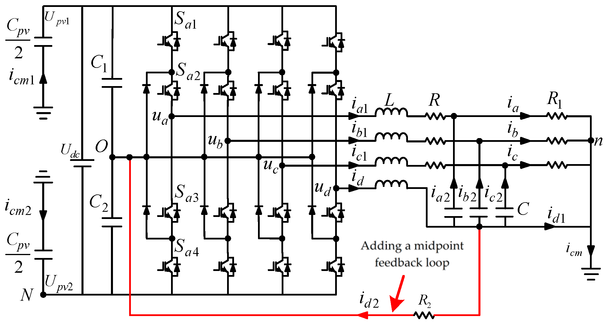
The existence of the parasitic capacitance between the photovoltaic array and the ground forms a common-mode resonant circuit that generates leakage current, posing risks to the safety and stability of the system. The schematic diagram of leakage current generation is shown in
Figure 1. In the figure,
Cpv is the parasitic capacitance between the solar panel and the ground;
upv1 and
upv2 are the parasitic capacitance voltages of the positive and negative buses, respectively.
C1 and
C2 are the positive and negative bus voltage-dividing capacitors on the DC side; L is the bridge arm filter inductor;
C is the filter capacitor;
O is the midpoint of the positive and negative bus capacitors on the DC side;
n is the neutral point of the load, and the current icm flowing from n to the ground is the leakage current.
Figure 1 shows the traditional three-level three-phase four-leg photovoltaic energy storage inverter topology [
26], which will be referred to as the traditional topology later.
The inverter adopts a carrier modulation strategy as a whole. The fourth bridge arm uses a positive and negative sequence separation method, mainly to improve the symmetry of the output voltage under unbalanced load conditions, and finally strike a balance between the suppression effect and the assurance of system performance.
2.1. Mathematical Modeling and Analysis of Common-Mode Loop in Traditional Topology Structure
According to Kirchhoff’s voltage law, the following equations can be listed:
ua, ub, uc, ud are the voltages from point O to N of the output of each bridge arm; ia1, ib1, ic1, id1 are the output currents of the bridge arms; ia, ib, ic are the load currents; R1 is a three-phase load; unN is the voltage of the neutral point on the load side relative to point N.
The formula for the midpoint voltage difference can be expressed as follows:
where P is the positive terminal of the DC bus, and N is the negative terminal of the DC bus.
The leakage current can be expressed as follows:
The current of the capacitor branch is defined as follows:
The current of the three-phase load branch is defined as follows:
The voltage difference
unN between the neutral point n of the load end and point
N can be expressed as follows:
Since the parasitic capacitances of the positive and negative DC buses to the ground are the same, and the currents flowing through them are also the same, there are the following:
Substituting Equation (7) into Equation (6), we can obtain the following:
From the topology of
Figure 1, the following equations can be formulated:
Among them,
icm1 and
icm2 are the leakage currents generated by the parasitic capacitances of the positive and negative buses to the ground, respectively. It can be obtained from Equations (8) and (9):
Select point
N on the DC bus side as the common-mode voltage reference point. The common-mode voltage is defined as the arithmetic mean of the voltages of the four-phase bridge arms output to point
N. Then we can obtain the following:
By rearranging Equations (1)–(11), the common-mode voltage equation for the common-mode loop is obtained:
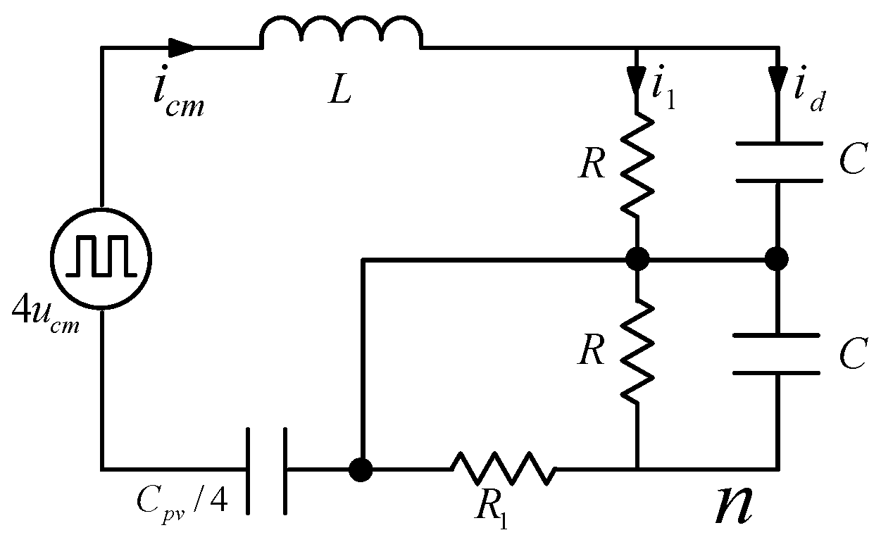
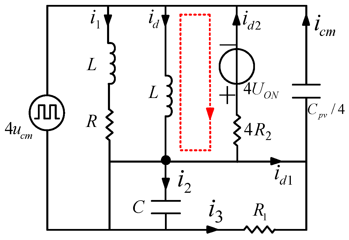
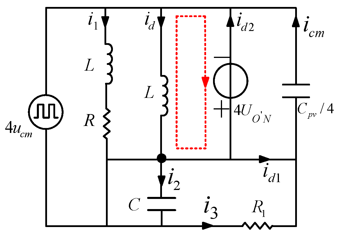
Based on Equation (12), the equivalent circuit of the common-mode loop for the inverter under the traditional topology is derived as shown in
Figure 2.
Based on Equation (12), the equivalent circuit of the circuit shown in
Figure 1 is derived, and its specific form is presented in
Figure 2. As indicated in
Figure 2, the excitation source of this equivalent circuit is the common-mode voltage 4
ucm. Without changing the original component parameters, the leakage current
icm can be suppressed through two core methods: First, optimize the excitation mode and control strategy to reduce the slew rate of the common-mode voltage, thereby indirectly mitigating the leakage current. Second, modify the circuit topology based on the principles of the hardware circuit to achieve direct suppression of the leakage current.
2.2. Leakage Current Analysis of Traditional Topology
The simulation experiment is carried out on the MATLAB(R2022b)/Simulink platform. The parameter settings are shown in
Table 1. According to the active power of about 50 nF~150 nF/kW, the parasitic capacitance value is 1 μF.
To control variables, the simulation parameters for the subsequent optimized topology are set as shown in
Table 1.
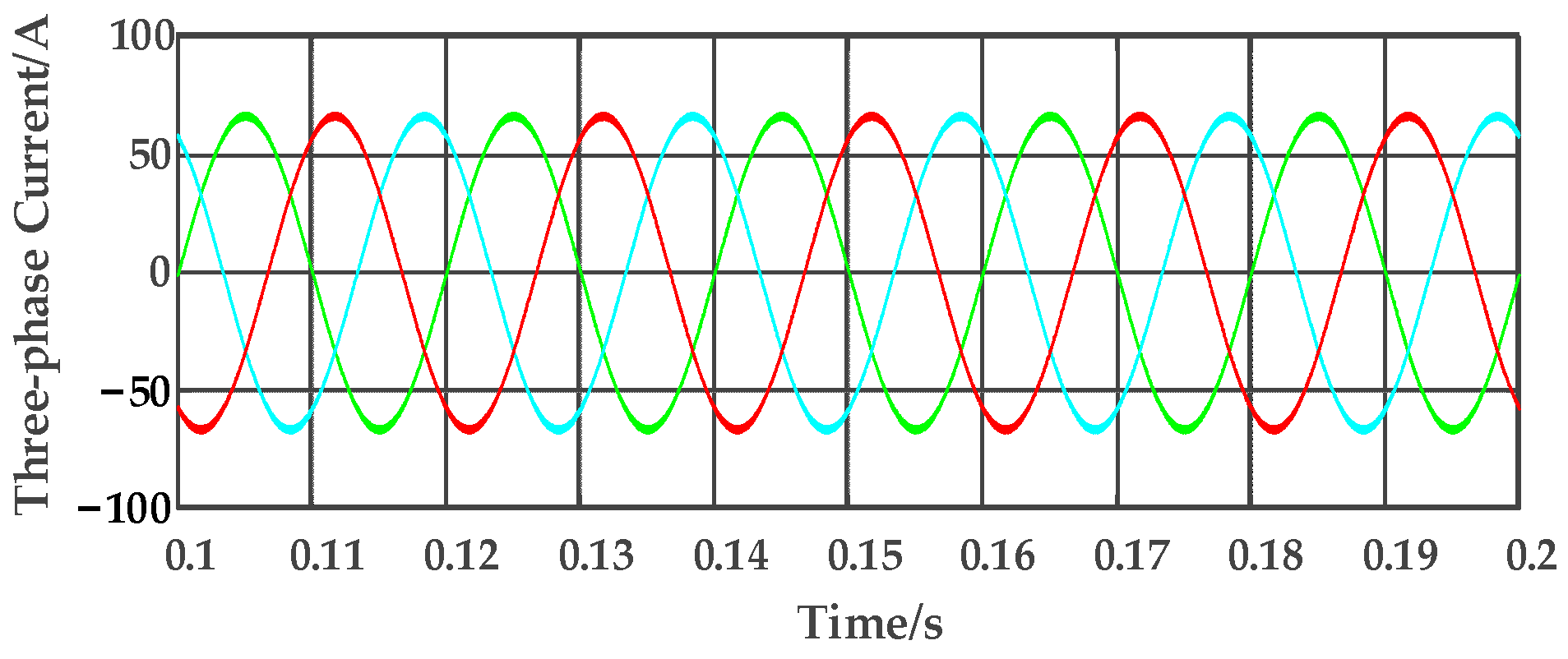
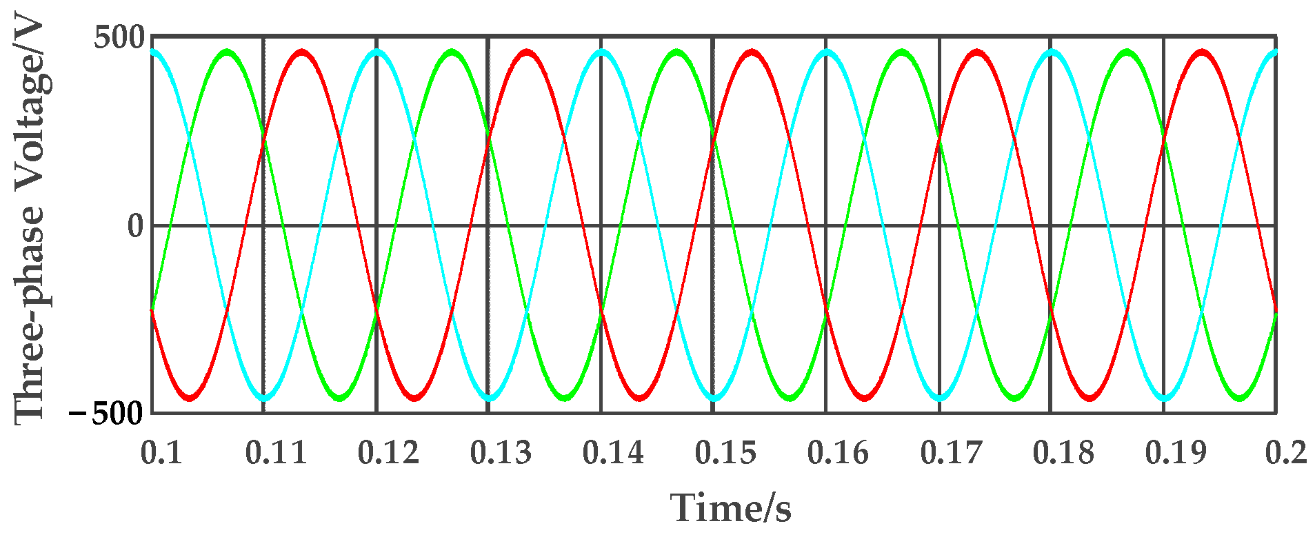
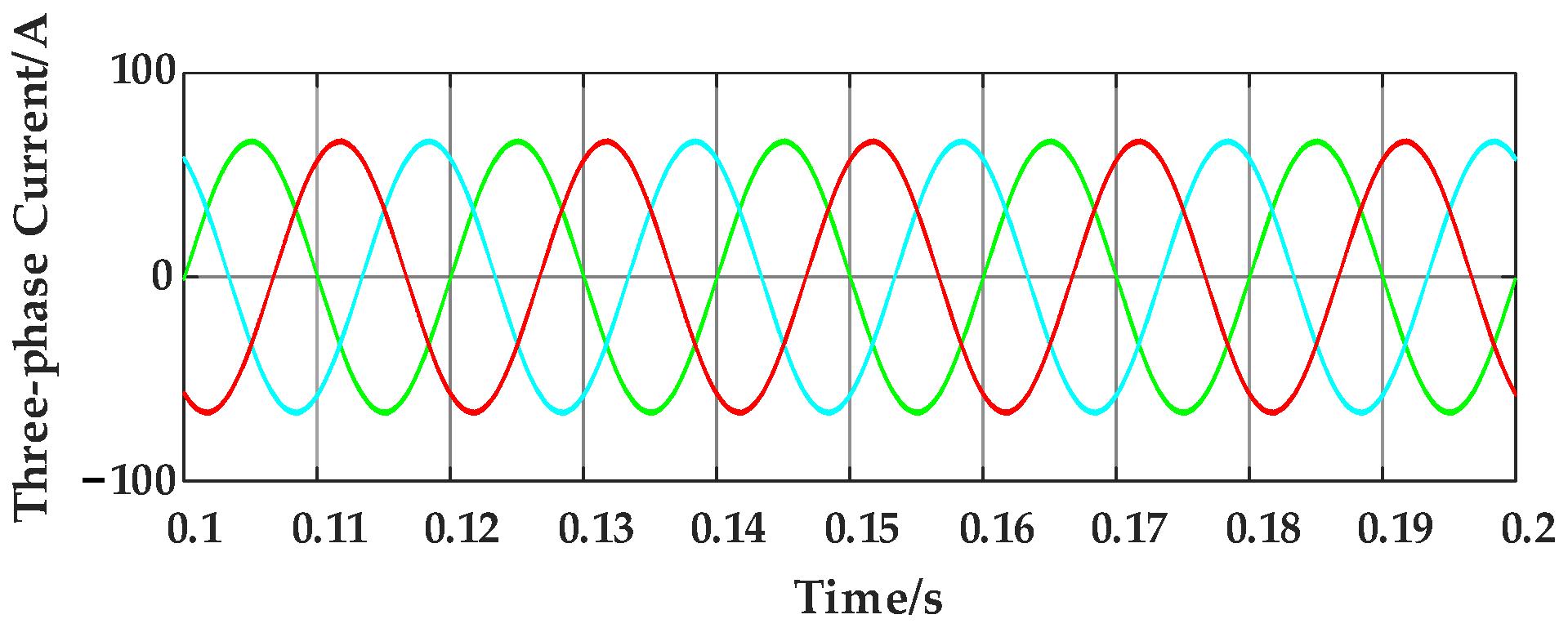
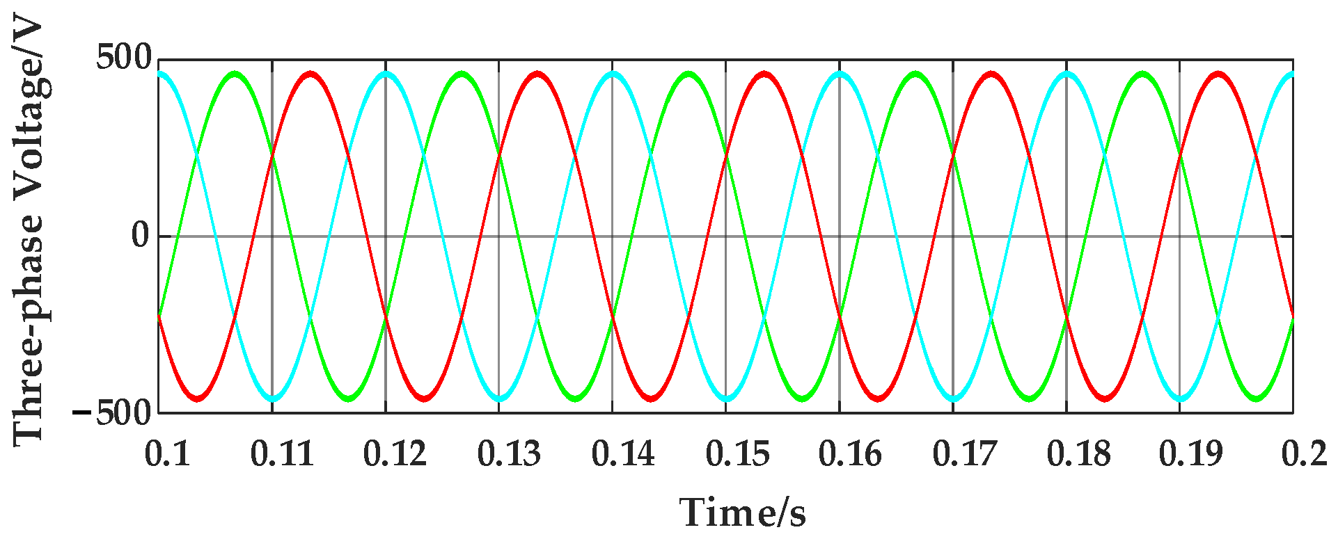
Under the traditional topology, the load-side current and voltage waveforms are shown in
Figure 3 and
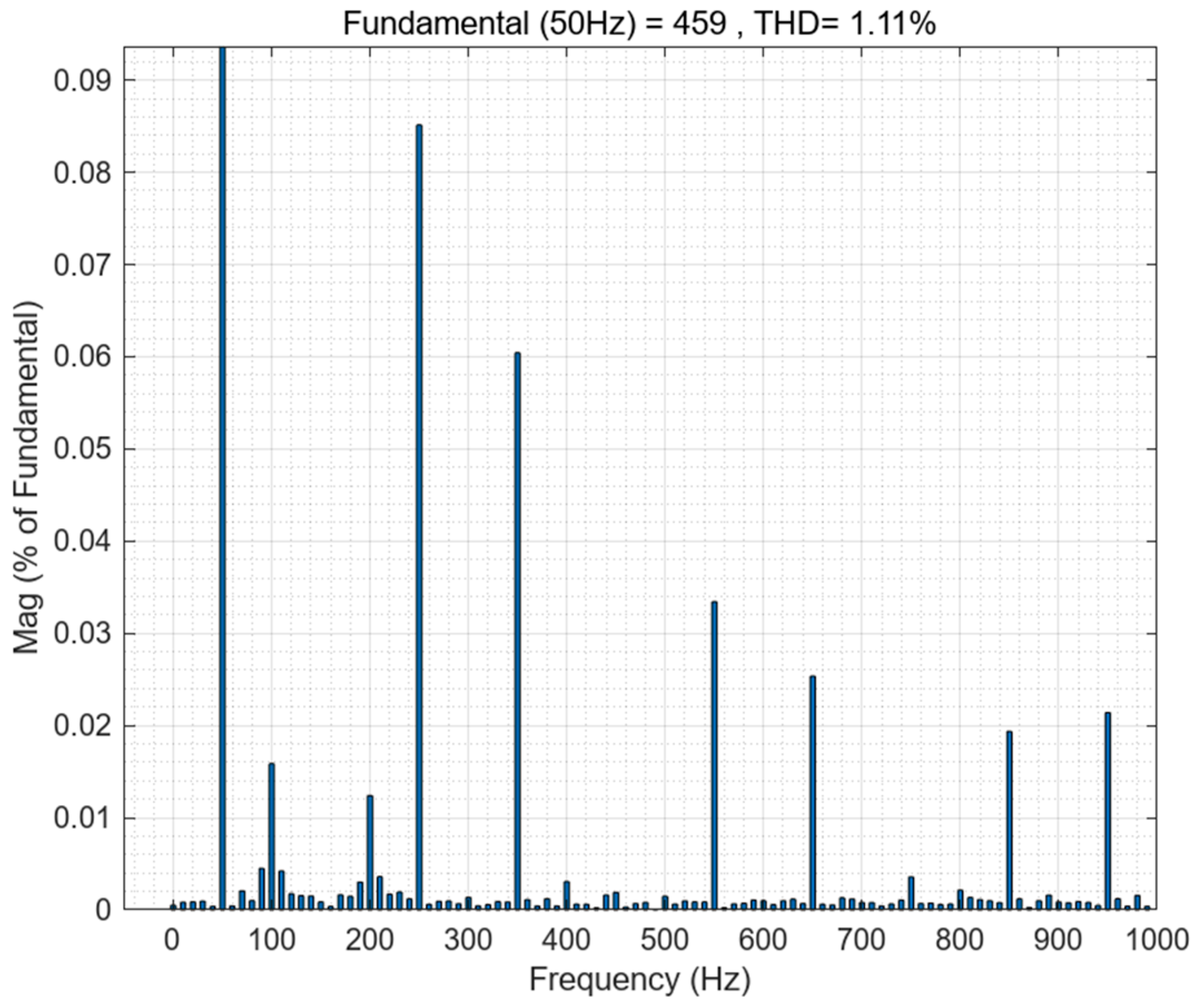
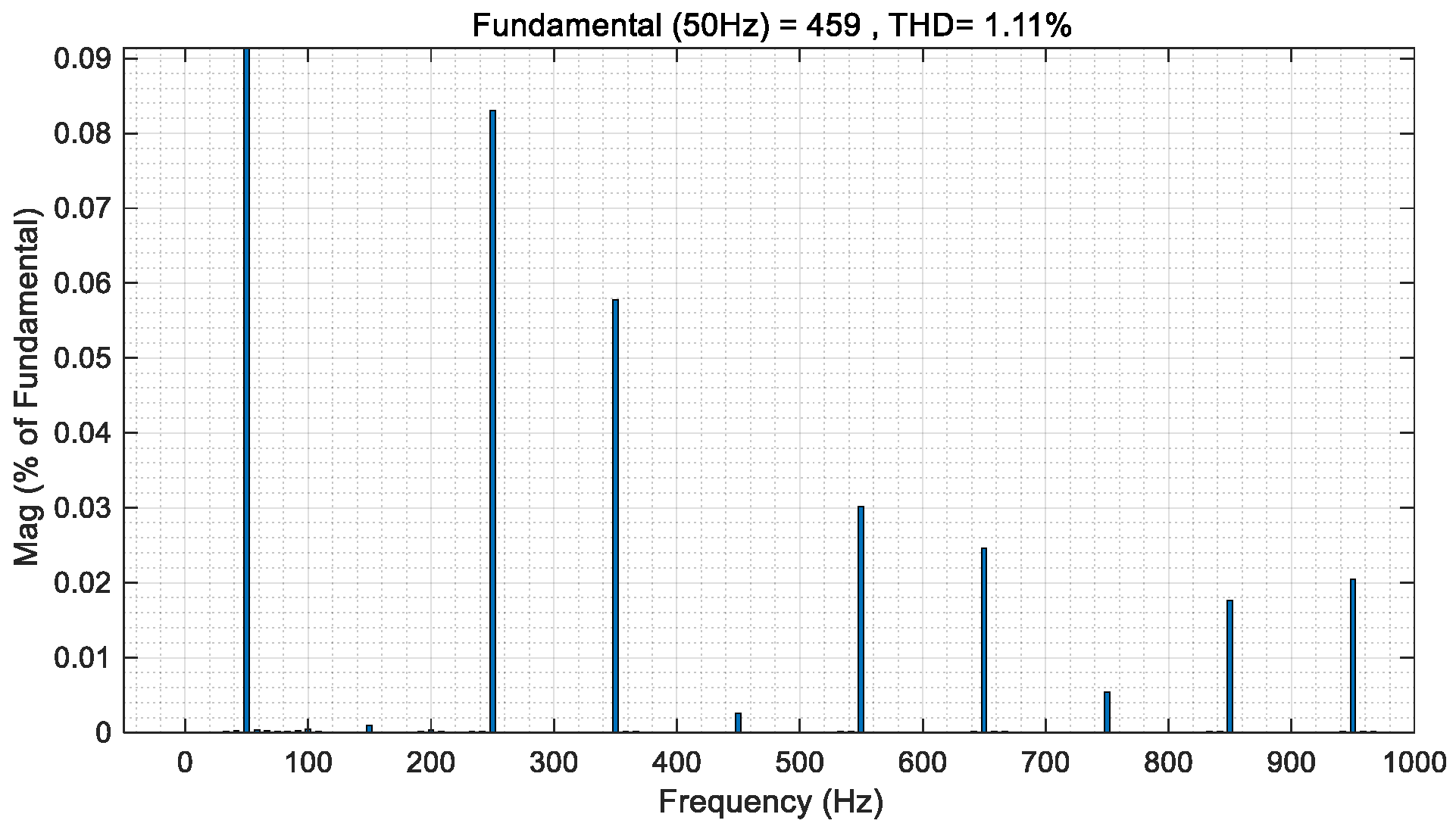
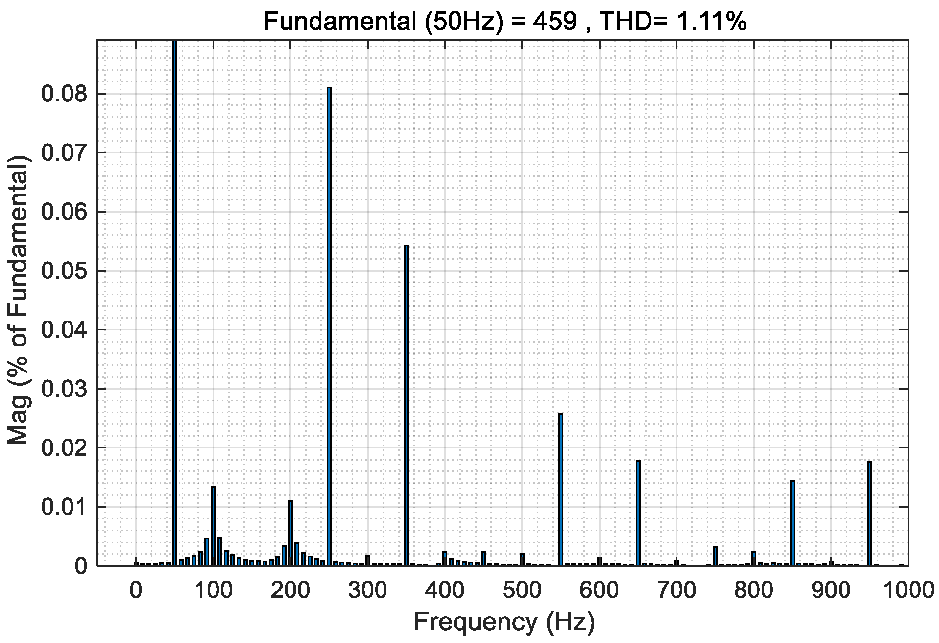
Figure 4, respectively. After the load-side current reaches a steady-state operating condition, Fast Fourier Transform (FFT) analysis is performed on the load-side voltage waveform, with the results presented in
Figure 5. As can be clearly observed from
Figure 5, the total harmonic distortion (THD) of the load-side voltage under this operating condition is 1.11%. This THD value objectively reflects the degree of voltage waveform distortion, providing a quantitative basis for evaluating the power quality of the traditional topology.
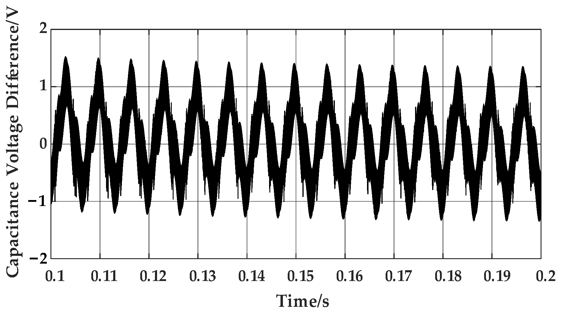
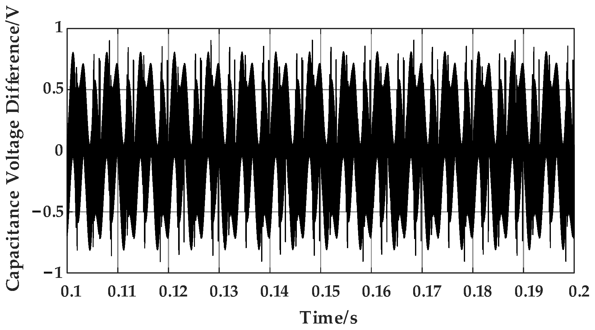
Figure 6 shows the voltage difference waveform across the two DC-side voltage-dividing capacitors, and
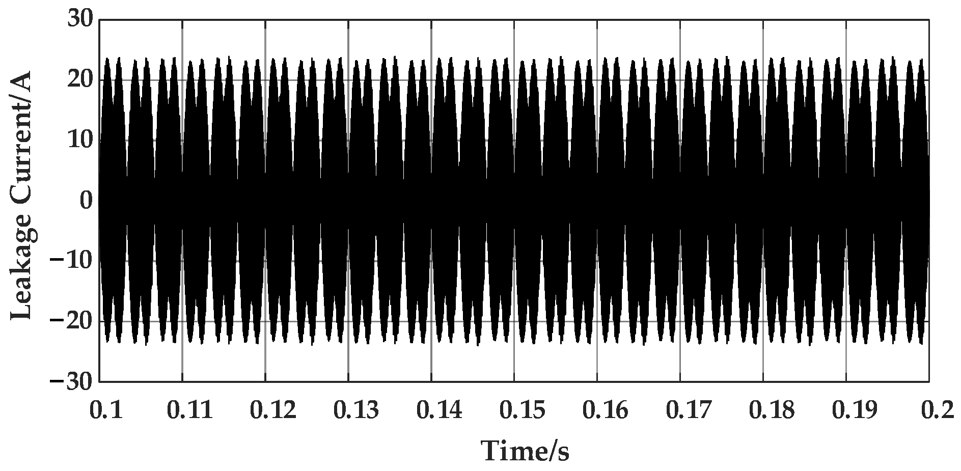
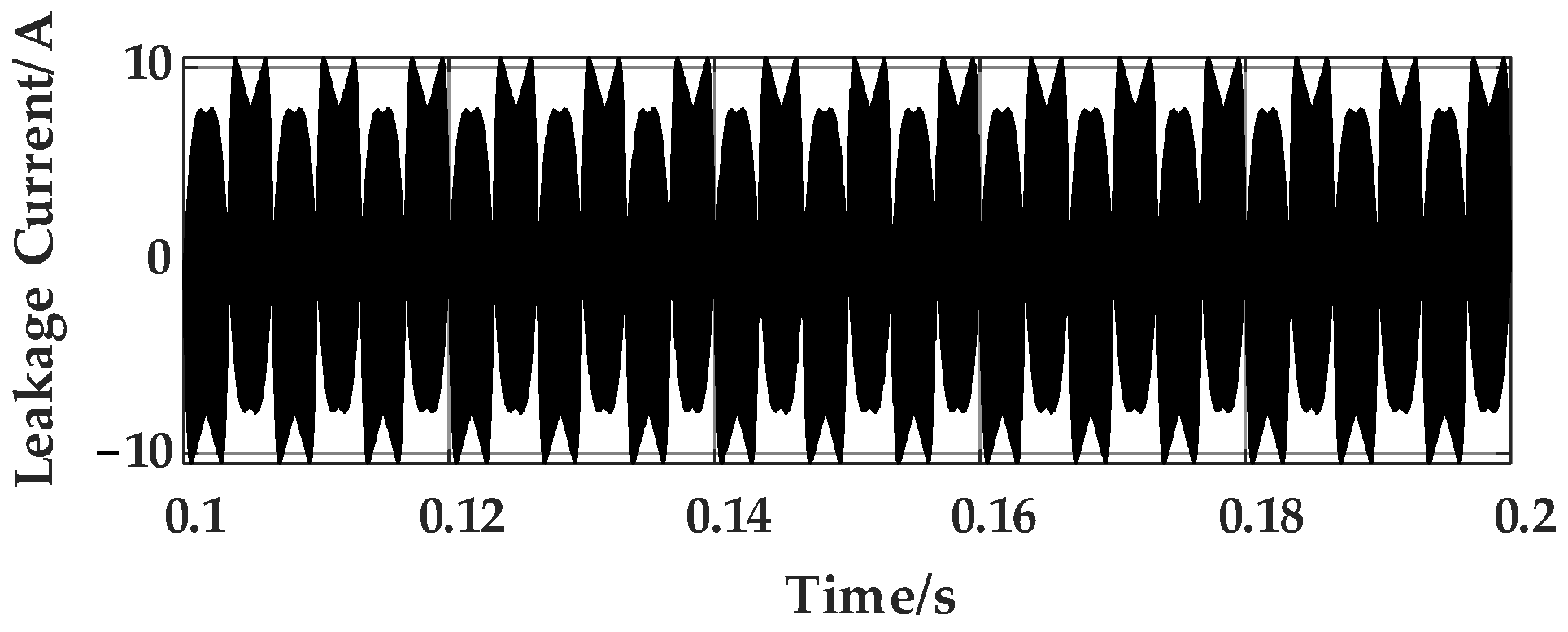
Figure 7 presents the leakage current waveform of this topology. A comprehensive analysis of the simulation results from
Figure 3,
Figure 4,
Figure 5,
Figure 6 and
Figure 7 indicates that, under the current control strategy, the fluctuation in the DC midpoint potential is maintained within 2 V. The suppression of leakage current is moderately effective, and the current distortion at the load end is relatively low. However, it should be noted that this strategy still has significant drawbacks: the maximum leakage current reaches 20 A, exceeding the safe operating threshold and posing considerable safety hazards. Therefore, further optimization of the three-phase four-leg topology is required to achieve the coordinated suppression of leakage current and midpoint potential fluctuations, thereby improving the system’s safety performance and operational stability.
4. Neutral Point Feedback Type II Topology Based on Independent Split Capacitor
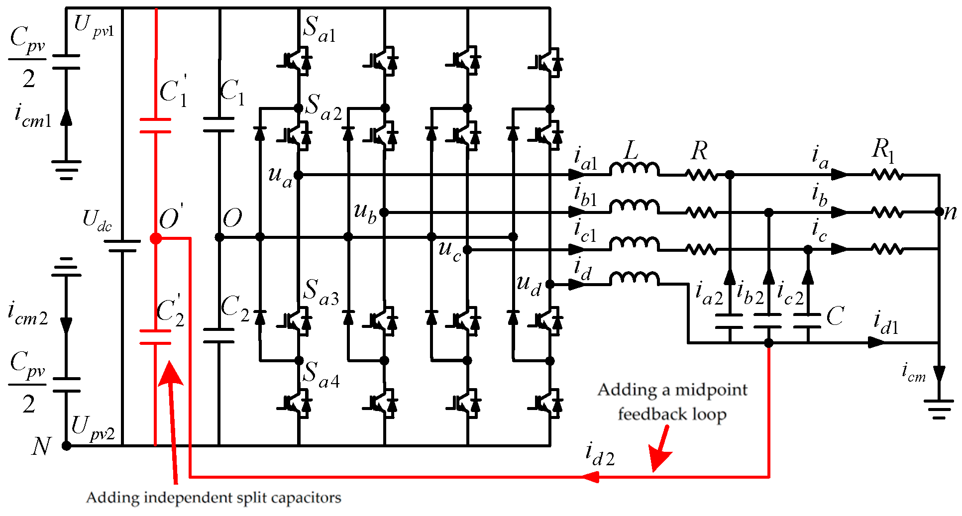
This paper proposes a leakage current suppression structure based on independent split capacitors. In this structure, Capacitors
and
serve as independent split capacitors between the positive and negative DC buses, with their capacitance values much smaller than those of the main DC-side capacitors
and
. The neutral point of the output filter capacitor is connected to midpoint
of the DC-side independent split capacitors. This connection method avoids the risk of direct grounding of the DC-side midpoint while providing an additional shunt path for the leakage current branches, thereby achieving leakage current suppression. The specific configuration of this improved topology is illustrated in
Figure 14.
Figure 14 illustrates the three-level four-leg photovoltaic energy storage inverter topology based on independent split capacitors, hereinafter referred to as the midpoint feedback Type II topology. Based on this topology, the corresponding equivalent circuit is shown in
Figure 15.
As illustrated in
Figure 15, compared with the traditional topology and the midpoint feedback Type I topology, the midpoint feedback Type II topology adds a new branch to the leakage current path. Theoretically, this branch plays a moderate role in suppressing leakage current. Meanwhile, the current is fed back to neutral point
of the independent split capacitors, which does not affect the DC bus midpoint, thereby enhancing system stability.
4.1. Mathematical Modeling and Analysis of Common-Mode Loop with Midpoint Feedback Type II Topology Structure
For the midpoint feedback Type II topology illustrated in
Figure 14, the leakage current loop equation is identical to Equation (1). Based on Kirchhoff’s Voltage Law (KVL), the following equation can be derived for the midpoint feedback loop:
where
denotes the voltage between the midpoint of the split capacitors and the midpoint of the bus capacitors. With point
N uniformly adopted as the voltage reference point for the modeling equations, the voltages of
and
are superimposed and uniformly expressed as
, and the above equations are rewritten as follows:
The leakage current under this condition is given by Equation (14).
It is not difficult to derive the leakage current loop equation from
Figure 14, which is completely consistent with Equation (15). By combining and organizing Equation (18), the midpoint feedback loop equation is obtained as shown in Equation (19).
At this time, the resonant frequency of the common-mode circuit can be obtained:
The independent split capacitor only affects the system’s common-mode resonant frequency fres_cm, while its interference with the differential-mode resonant frequency fres_dm is negligible. Leveraging this characteristic, the capacitance range of the independent split capacitor can be constrained based on the requirements for common-mode resonance suppression. Through the reasonable selection of capacitor parameters, this method ensures that the system maintains high common-mode filtering performance while delivering higher power quality to the load side.
4.2. Calculation of Capacitance Value of Neutral Point Feedback Type II Topologically Independent Split Capacitor
A reasonable capacitance value for the independent split capacitor can effectively mitigate low-frequency oscillation of the bridge arm–side current and reduce the effective value of the line current. Next, the basis and principles for selecting the capacitance value are discussed.
The expression of the low-frequency component in the common-mode voltage source [
27], the harmonic coefficient f(
n), and the harmonic source frequency
fres in the Fourier expression of the common-mode voltage are as follows:
where
n denotes the harmonic order;
Em is the phase voltage amplitude;
udc represents the DC bus voltage; and
f stands for the load-side frequency.
In engineering practice, it is generally accepted that when the harmonic component coefficient f(n) < 0.001, the influence of that harmonic order may be considered negligible. Based on this criterion, the minimum frequency of the harmonic source fres_min, can be calculated. If the system’s common-mode resonance frequency fres_cm, exceeds fres_min, the circuit can avoid generating common-mode resonance. Concurrently, to ensure the system possesses high-frequency filtering capability, the common-mode resonance frequency must be less than half the switching frequency fs (i.e., fres_cm < 0.5 fs). In summary, when the common-mode resonance frequency satisfies fres_cm ∈ [fres_min, 0.5 fs], the circuit can both avoid common-mode resonance and achieve high-frequency filtering. Substituting the DC-side electromotive force Em = 270 V and DC bus voltage Udc = 680 V into Equation (21) yields the specific constraint range for the common-mode resonance frequency:
To satisfy the condition for neglecting harmonic components with coefficients f(n) < 0.001, a harmonic order of n = 7 is selected. Substituting it into Equation (22) yields the following: the minimum frequency fres_min = 1.95 kHz for harmonic sources with sufficiently negligible amplitude impact. Combining this with the preceding switching frequency constraint 0.5 fs = 8 kHz, the effective range for the common-mode resonance frequency is further determined as fres_cm ∈ [1.95 kHz, 8 kHz]. Analyzing the common-mode resonance frequency calculation formula (20), it is evident that the independent split capacitance value C’ decreases as fres_cm increases, ultimately approaching 9.32 μF. Balancing engineering selection convenience with performance requirements, C’ = 9 μF was selected for simulation analysis. This parameter ensures the circuit avoids common-mode resonance while effectively limiting the feedback current in the LC circuit.
4.3. Leakage Current Analysis of Neutral Point Feedback Type II Topology
The simulation results of the midpoint feedback Type II topology are illustrated in
Figure 16,
Figure 17,
Figure 18,
Figure 19 and
Figure 20. The physical quantities depicted in each figure and their analyses are as follows:
Figure 16 presents the load-side current waveform, reflecting the dynamic response and steady-state characteristics of the load current;
Figure 17 shows the load-side voltage waveform, which is used to observe the amplitude stability and waveform smoothness of the output voltage;
Figure 18 displays the Fast Fourier Transform (FFT) analysis results of the load-side current after the system reaches stability, enabling quantitative evaluation of the total harmonic distortion (THD) to measure power quality;
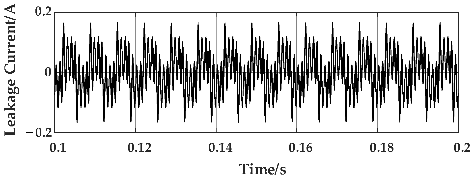
Figure 19 depicts the leakage current waveform, intuitively demonstrating the leakage current suppression effect of this topology;
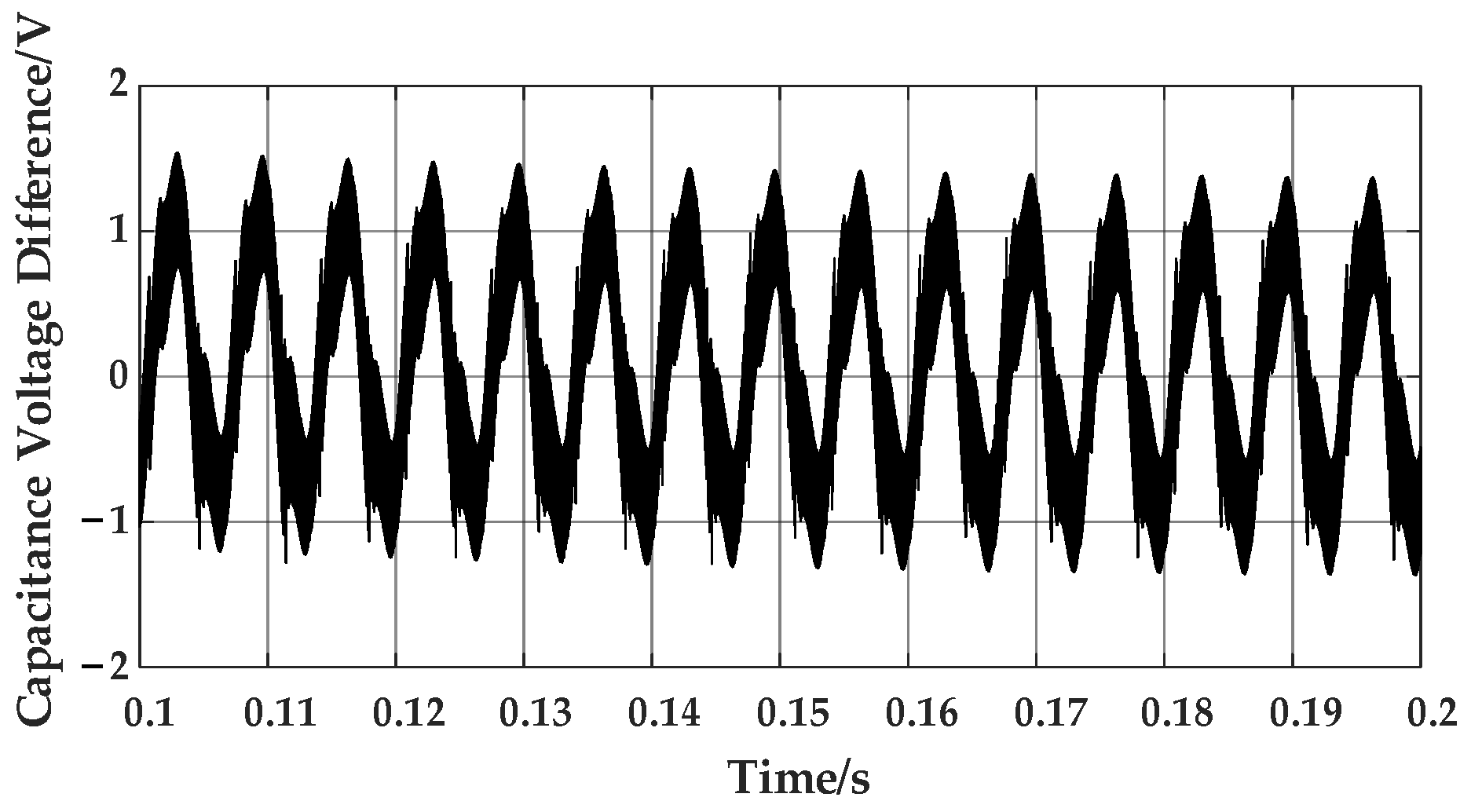
Figure 20 provides the voltage difference waveform between the two voltage-dividing capacitors on the DC side under the optimal topology scheme, which is used to analyze the balance of the midpoint potential on the DC side.
As can be seen from
Figure 18, the current distortion rate (i.e., total harmonic distortion, THD) of the load side under the midpoint feedback Type II topology is 1.11%, indicating that the output power quality meets the relevant standards.
According to China’s energy industry standard NB/T 32004-2018 “Technical Specification for Photovoltaic Grid-Connected Inverters” and national standard GB/T 20321-2023 “Inverters for Off-Grid Wind and Solar Power Generation Systems”, for inverters with a rated output of less than 30 kVA, the leakage current requirement is no more than 300 mA. As illustrated in
Figure 19, the maximum leakage current of the midpoint feedback Type II topology is 165 mA, which meets the requirements of China’s energy industry standard.
5. Analysis of Experimental Results
Building upon the validation of the aforementioned simulation results, this study further constructed a physical experimental platform with parameters consistent with those of the simulations to verify the practical operational performance of the optimized topology.
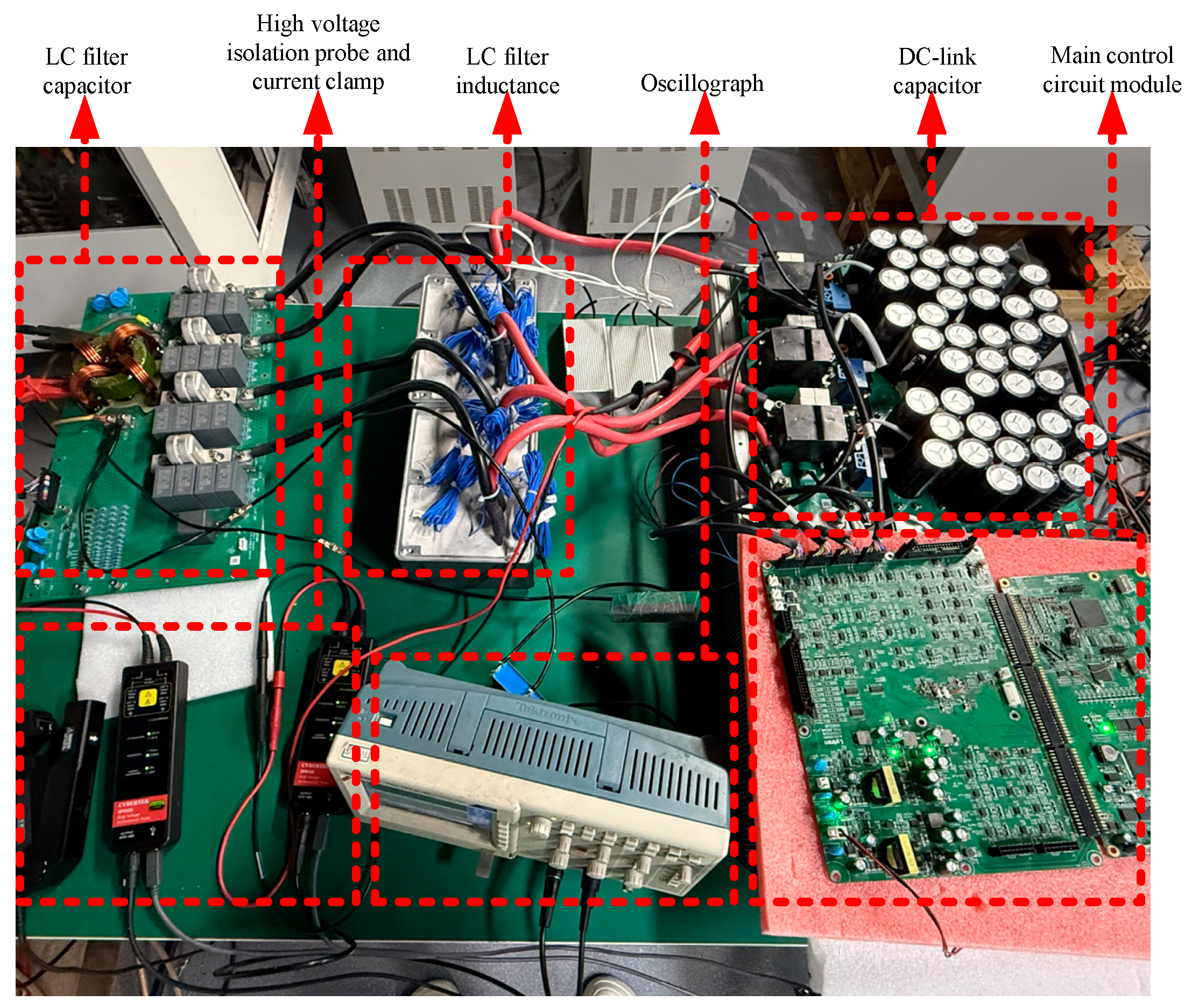
Figure 21 presents the overall configuration of the three-level three-phase four-leg inverter experimental platform utilized in this research. Comprising a main circuit module, a control module, a sampling module, and a load module, the platform facilitates real-time monitoring of the topology’s operational status and accurate data acquisition.
A detailed description of the equipment used in the experiment is as follows: the oscilloscope was manufactured by TektronixTektronix, model TDS 1012C-SC, with its headquarters located at 14150 SW Karl Braun Drive, Beaverton, OR 97077, USA; the voltage probe was a high-voltage isolation probe produced by CYBERTEK (Shenzhen ZhiYong Electronics Co., Ltd., Shenzhen, China), model DP615, and the company is situated at Unit A1702-1, No.1 Workshop, Longgang Tian’an Digital Entrepreneurship Park, No.441 Huangge Road, Longgang District, Shenzhen, Guangdong, China; the current probe was a current clamp manufactured by CYBERTEK (Shenzhen ZhiYong Electronics Co., Ltd.), model HCP8300, with the same company address as above; the photovoltaic simulation DC source adopted the solar array simulator of Parwa (Shenzhen Parwa Technology Company Limited), with a maximum output voltage of 600 V, and the company is located at Floor 6, Block 5, Nangang Second Industrial Park, Xili Town, Nanshan District, Shenzhen, Guangdong, China.
To verify the performance advantages of the proposed “three-level three-phase four-leg topology with independent split capacitors on the DC bus,” a comparative experiment was designed. When the DC bus voltage is set to 600 V, the traditional three-level three-phase four-leg topology and the improved topology proposed in this paper adopt the same carrier modulation strategy for parallel experiments.
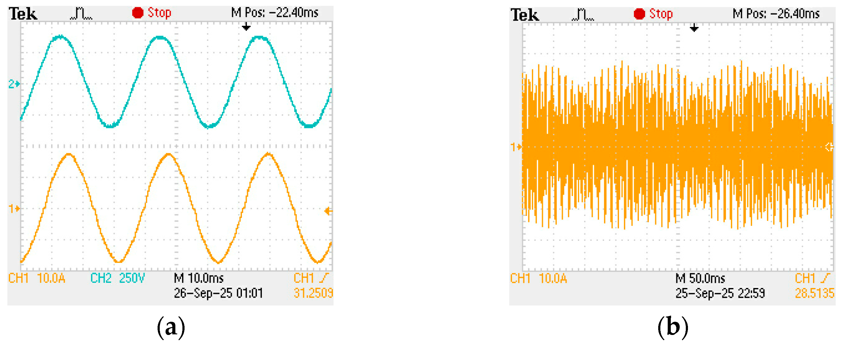
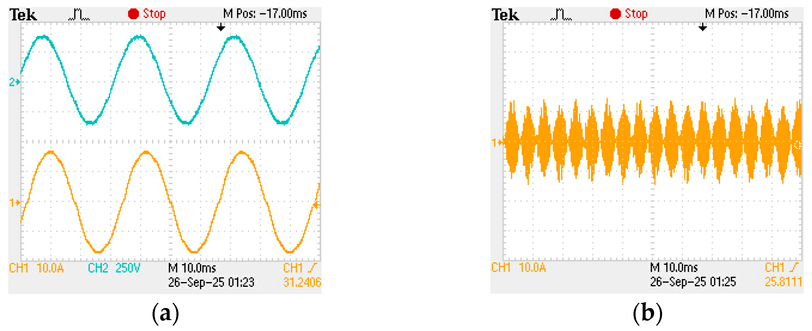
Figure 22 presents the first set of experimental results of the traditional topology. Although the load-side line voltage of phases a and b and the phase a current waveform maintain sinusoidal characteristics, the peak leakage current of the traditional topology reaches as high as 26 A. This leakage current value far exceeds the safe operation threshold, which may damage equipment insulation and pose significant safety hazards to personnel. This highlights the major flaw of the traditional topology in leakage current suppression.
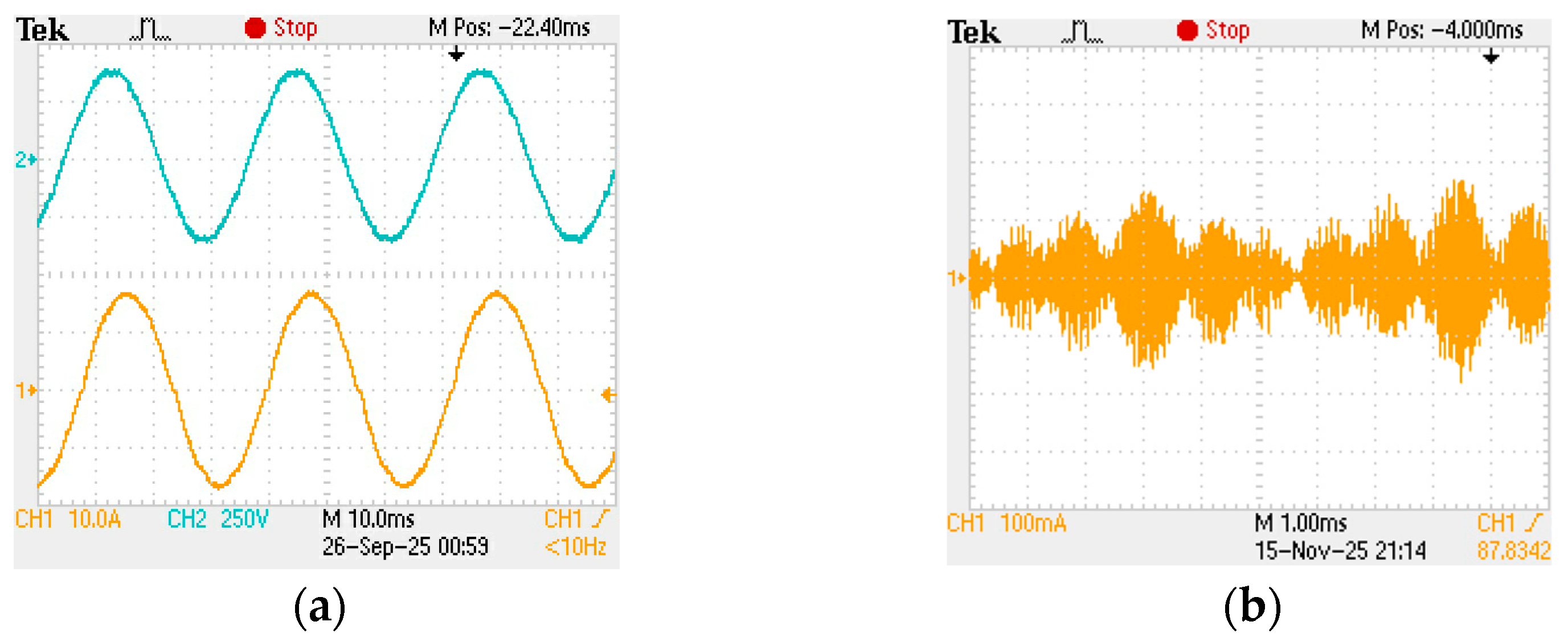
Figure 23 presents the waveforms of the phase a–b voltage and phase a current obtained from the experiment on the midpoint feedback Type I topology. At this point, the peak leakage current is approximately 14 A, which is significantly reduced compared with the traditional topology but fails to meet the engineering requirements.
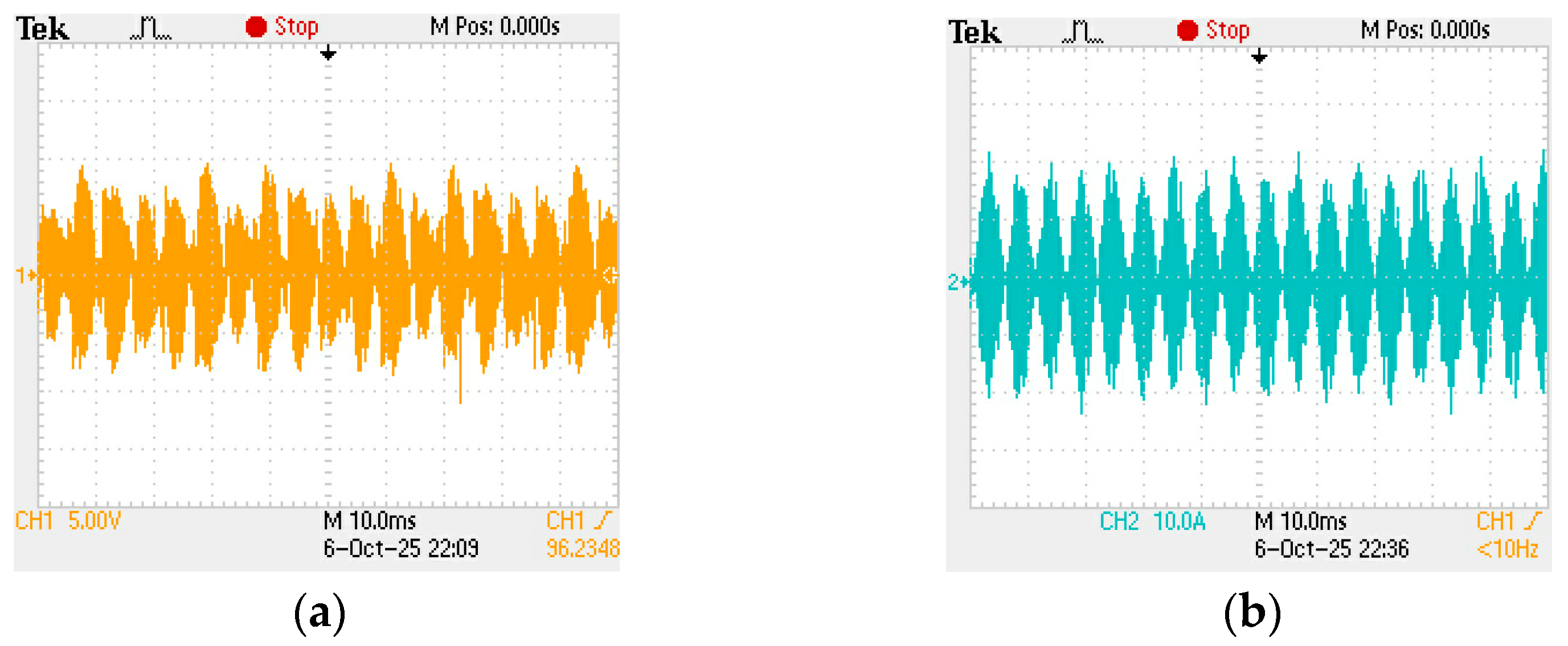
Figure 24 illustrates the experimental waveforms of the proposed “three-level three-phase four-leg inverter with independent split capacitors” under a DC bus voltage of 600 V, including the load line voltage waveform, load line current waveform, and leakage current waveform. As is clearly shown in
Figure 24, both the load line voltage and line current waveforms are very close to standard sine waves with low distortion. At this point, the peak leakage current is approximately 185 mA, which is almost identical to the simulation result (165 mA). Considering that the simulation parameters are idealized and the difference is negligible, the experimental results basically meet the expectations.
Building on the experimental results in
Figure 24, further experiments and analyses were conducted on the midpoint feedback Type II topology.
Figure 25 illustrates the voltage fluctuation waveform of the midpoint of the DC bus capacitors and the current waveform between the load-side point
n and the midpoint of the split capacitors. The figure shows that the fluctuation amplitude of the midpoint potential of the DC bus capacitors is consistently within 10 V, indicating that this topology provides effective voltage balance control for the bus. In this experiment, the independent split capacitors consist of two 10 μF capacitors connected in series. Experimental data demonstrate that the peak current flowing from the load-side point
n to the midpoint of the split capacitors is approximately 20 A. It should be noted that the independent split capacitors are connected in parallel with the DC bus capacitors in the circuit. This topology relies on the independent split capacitors to carry the load-side feedback current, effectively suppressing midpoint potential drift and thus ensuring the operational stability of the DC bus midpoint.
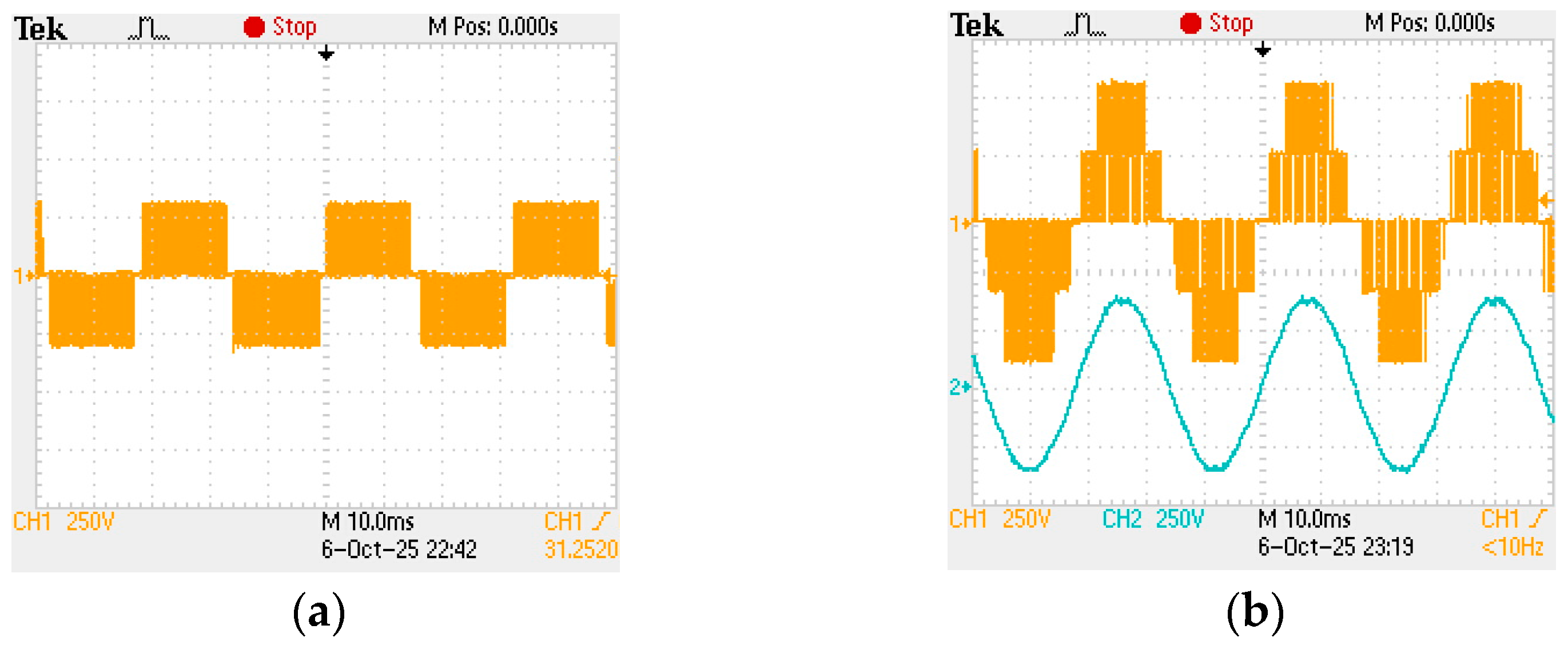
Figure 26 illustrates the key output waveforms of the proposed “three-level three-phase four-leg inverter based on independent split capacitors,” specifically including the output voltage waveform of Leg A, the output line voltage waveform of Legs A and B, and the load-side line voltage waveform of phases a and b. The experimental waveforms show that the line voltage of Legs A and B exhibits a typical five-level characteristic (i.e., five discrete voltage levels), which is consistent with the output voltage performance of the three-level topology. After processing by the output filter circuit, both the load-side line voltage of phases a and b and the corresponding line current waveform are close to the standard sinusoidal form with excellent smoothness, verifying the effectiveness of the filter scheme for this topology.
Based on comprehensive simulation and experimental data, the peak leakage current performances of different topologies are as follows: the traditional topology has a simulated value of 24 A and an experimental value of 26 A; the midpoint feedback Type I topology has a simulated value of 11 A and an experimental value of 14 A; while the proposed midpoint feedback Type II topology has a simulated value of only 165 mA and an experimental value of 185 mA. The simulation and experimental results are largely consistent, verifying the accuracy of the analytical model. From the experimental data, it is clearly observed that the midpoint feedback Type II topology exhibits a significant leakage current suppression effect compared to the traditional topology. This advantage stems from the introduction of independent split capacitors: these capacitors provide an additional active discharge path for the common-mode leakage current. Without interfering with the system’s original control logic or overall stable operation, the magnitude of the leakage current flowing to the ground is greatly reduced.
In conclusion, the “three-level three-phase four-leg topology with independent split capacitors on the DC bus” proposed in this paper achieves effective leakage current suppression through the synergistic action of the common-mode shunting effect provided by the independent split capacitors and the midpoint potential stabilization mechanism. At the same time, the voltage and current waveforms on the load side maintain good sinusoidal characteristics, meeting the power quality requirements. Particularly importantly, this topology can achieve an excellent balance between leakage current suppression performance and system operational stability without the need for designing additional control strategies, which fully verifies its technical feasibility and advantages for engineering applications.