Article

Optimizing Periodic Intervals in Multi-Stage Waveguide Stub Bandstop Filters for Microwave Leakage Suppression

1
Department of Elecrical, Electronic and Communications Engineering, Faculty of Science and Engineering, Kawagoe Campus, Toyo University, 2100 Kuzirai, Kawagoe 350-8585, Saitama, Japan
2
Department of Electronic Engineering, National Kaohsiung University of Science and Technology, No. 1, University Rd., Yanchao Dist., Kaohsiung 824005, Taiwan
3
Department of Electronic Systems Engineering, Takuma Campus, National Institute of Technology, Kagawa College, 551 Kouda, Takuma, Mitoyo 769-1192, Kagawa, Japan
*
Author to whom correspondence should be addressed.
Electronics 2025, 14(23), 4660; https://doi.org/10.3390/electronics14234660
Submission received: 5 October 2025 / Revised: 16 November 2025 / Accepted: 25 November 2025 / Published: 27 November 2025
(This article belongs to the Section Microwave and Wireless Communications)

Abstract

Waveguide bandstop filters (BSFs) play a key role in preventing electromagnetic wave leakage from gaps or sample entrances and exits, which can compromise safety, work efficiency, and electromagnetic compatibility. This study designs a waveguide BSF using a finite periodic structure of cascaded short-circuited E-plane stubs (chokes) to achieve a stopband with the transmission coefficient |S21| ≤ −30 dB and a 4% relative bandwidth. We investigate the impact of stub width on bandwidth broadening and stub spacing in cascade connections on spurious passband suppression. Electromagnetic and circuit simulations, validated experimentally, reveal that stub spacing at odd multiples of a quarter guided wavelength (λg/4) minimizes spurious passbands, with wider stubs and larger spacings enhancing stopband characteristics. This indicates that there is a great advantage in reducing the number of resonators and manufacturing costs. These findings provide practical and new design guidelines for designing efficient BSFs for preventing microwave leakage and may have applications in other filters or array antennas using periodicity.

1. Introduction

Microwave heating systems, used in industrial and domestic applications, rely on openings for the continuous insertion and removal of materials. However, these openings allow for electromagnetic wave leakage, posing safety risks to operators and interfering with nearby wireless systems. When the leakage of electromagnetic waves from an opening exceeds an acceptable level, it becomes necessary to intermittently shut down the oscillator or use a mechanical opening and closing mechanism such as a metal shutter, reducing work efficiency. Bandstop filters (BSFs) or a choke structure created by using E-plane waveguide discontinuity are essential to suppress this leakage, because the electric field component perpendicular to the opening easily leaks as radiated electromagnetic waves, even if the gap is narrowed [1,2,3]. When the gap is sufficiently narrow relative to the wavelength, treating it as a parallel plate results in low characteristic impedance, making the combined use of magnetic loss-based microwave absorbers effective [4,5]. Sufficient suppression of electromagnetic energy leaking through openings ensures safe operation, electromagnetic compatibility, and optimal energy utilization. In many waveguide-type BSF designs, the filter synthesis method is employed [6,7,8,9,10,11], necessitating stepwise modification of each resonator’s shape and spacing, increasing the complexity and manufacturing costs for waveguide circuits that require precise 3D metal machining. Recent advances in metal 3D printing technology show great promise [12,13], but it remains too expensive. An alternative approach utilizes periodic structures, where identically shaped resonators are arranged at regular intervals. This design simplifies implementation and, if integrated into substrate integrated waveguides (SIWs), can reduce production costs [14,15].
Previous BSF studies in periodic structure have demonstrated the use of a quarter guided wavelength (λg/4) short-circuited stubs in a corrugation or waffle-iron structure [16,17,18]. This waffle-iron filter was then utilized as a waffle ridge guide in transmission lines [19,20,21,22,23]. Furthermore, instead of utilizing a λg/4 line, a mushroom structure representing a compact LC parallel resonant circuit has been put into practical use [24,25,26,27,28]. These structures are known as Electronic Band Gap (EBG) or metamaterial.
However, these designs employ narrow-band LC parallel resonators with limited bandwidth and do not focus on the stub width. Furthermore, these periodic spacings are based empirically on λg/4. Our prior work revealed that widening the stub width in the transmission direction can widen the stopband [29,30,31], and if the stub width exceeds λg/4, the conventional λg/4 periodic interval cannot be applied. Furthermore, if the periodic interval deviates from λg/4, a spurious passband appears within the designed stopband. However, the mechanism behind its occurrence and methods to avoid it are not explained in detail. Therefore, this study aims to systematically investigate the interaction between stub width and cascade spacing in finite periodic structures, focusing on the suppression of spurious passbands and bandwidth maximization. We propose design guidelines for wideband stubs exceeding λg/4 in width, offering a practical solution for a high-performance waveguide-type bandstop filter for microwave leakage prevention.
Potential applications of this research include leak prevention filters for apertures in shutter-free microwave heating, where the heated object is continuously inserted and removed, and various microwave bandstop filters or array antennas that allow for a finite periodic arrangement in the transmission direction.
The paper is organized as follows: Section 2 examines single stub characteristics, Section 3 analyzes two-stage cascades, Section 4 explores multi-stage configurations, Section 5 presents experimental validation, and Section 6 summarizes key findings.

2. Characteristics of a Single Stub

2.1. Electromagnetic Field Simulation

A single stub’s bandstop characteristics were analyzed using Murata Software Femtet version 2025.0.2 [32] for electromagnetic (EM) field simulation. The model (Figure 1) places a short-circuited stub (width w, depth d) in the E-plane of a standard waveguide (a = 0.58 λg, b = 0.26 λg), where λg is the guided wavelength of the TE10 mode at 10 GHz (λg = 39.7 mm). The waveguide walls are PEC and filled with air. The port distance (l ≥ 1.0 λg) minimizes higher-order mode effects at both ends of the waveguide ports 1 and 2. The results of EM simulations can easily change depending on the mesh size. The initial mesh size is set to 3.0 mm, which is 1/10 of the free-space wavelength at 10 GHz. The frequency sweep range is from 9 GHz to 11 GHz, in 10 MHz intervals. Adaptive meshing ensures convergence of the S-parameters (accuracy ≤ 0.02). Since the dimensions of the standard waveguide are approximately b/a ≈ 0.5, using wavelength-normalized dimensions enables the use of the design for other frequency bands.
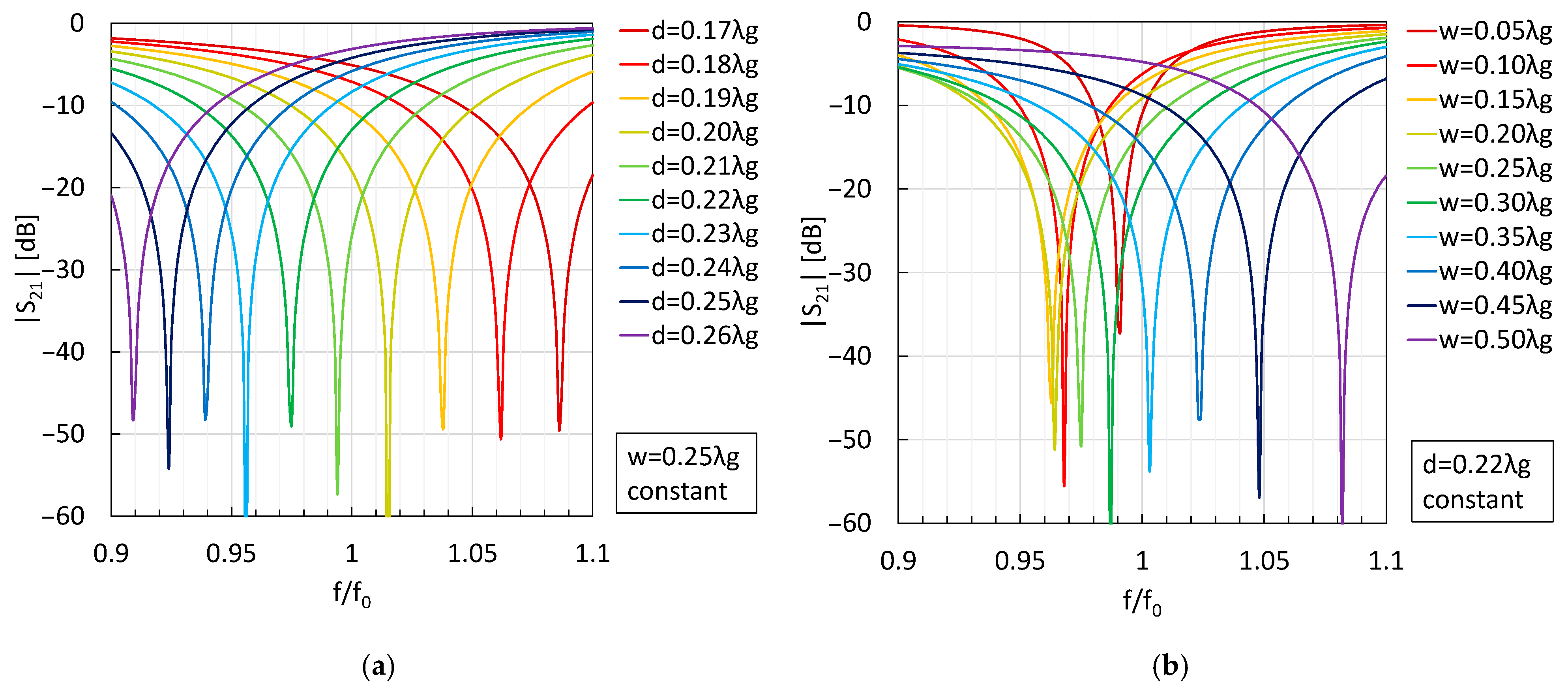
Figure 2 shows the parametric sensitivity analysis of a single stub. Figure 2a shows the change in transmission coefficient |S21| at ports 1 and 2 with respect to the change in the stub depth d when the stub width is fixed at w = 0.25 λg. The horizontal axis is normalized to 10 GHz. The legend indicates 10 stub depths (d = 0.17 λg to 0.26 λg). The resonant frequency decreases monotonically, with an increase in the depth d, indicating that the resonant frequency can be easily controlled by adjusting the depth d. As the resonant frequency decreases, the stopband width decreases slightly, but the rate of decrease is small. Figure 2b shows the change in |S21| with respect to changes in the stub width w when the stub depth is fixed at d = 0.22 λg. The legend shows the 10-stub width (w = 0.05 λg to 0.50 λg). As the width w increases, the resonant frequency initially decreases, reaches a minimum at w = 0.15 λg, and then increases again. The stopband width varies significantly with the value of w. To compare differences in stopband width, the resonant frequency must be set to the same value. Therefore, six stub widths (w = 0.05 λg to 0.40 λg) were tested, with depth d adjusted to maintain resonance at 10 GHz.
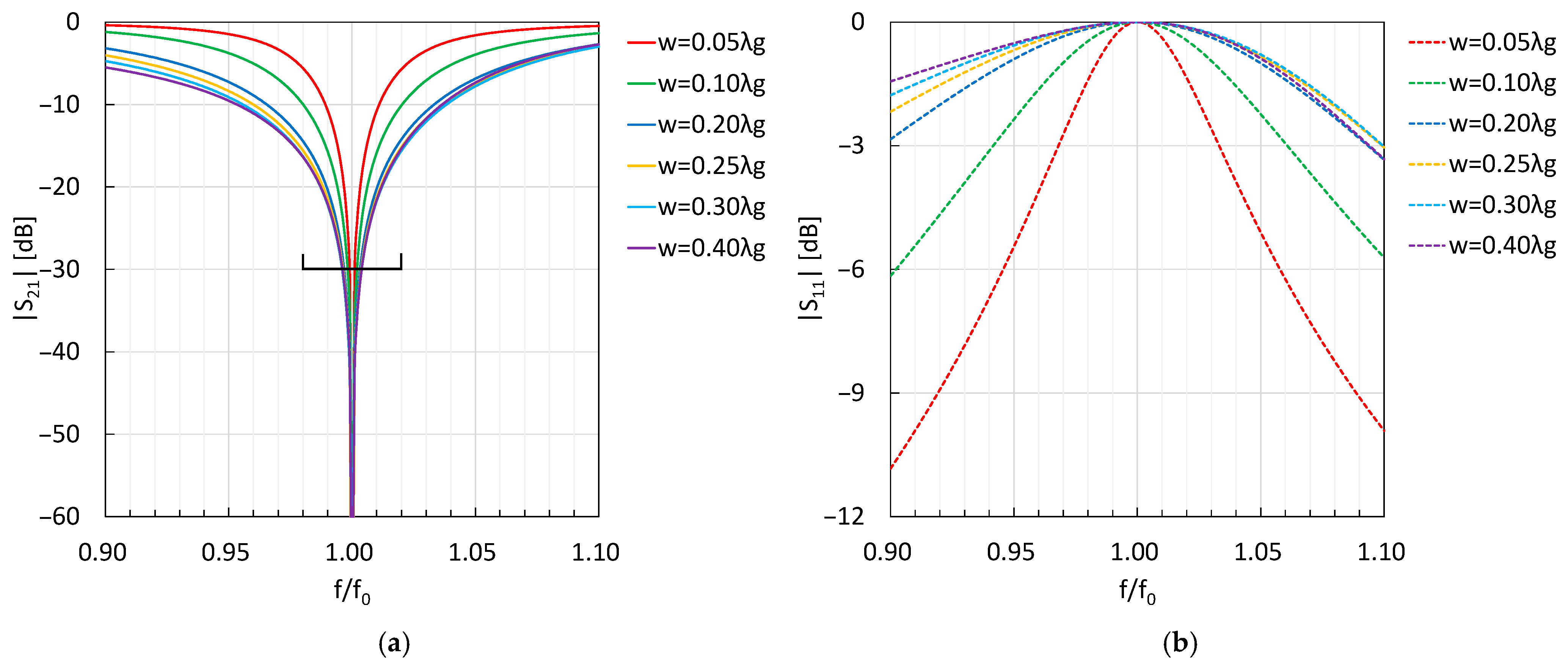
Figure 3 shows the bandstop characteristics of a single stub as a function of stub width. (a) shows |S21|, and (b) shows |S11|. The legend shows six stub widths (w = 0.05 λg to 0.40 λg), with solid lines indicating |S21| and dashed lines indicating |S11|. The target line is drawn for the required rejection level |S21| ≤ −30 dB and a 4% fractional bandwidth (FBW). Increasing the stub width changes the stopband width, but the change becomes small when the width exceeds w ≥ 0.20 λg.
Table 1 summarizes the calculated dimensions w, d, b and dimension ratios w/b used in the EM simulation, the normalized lower frequency limit fL/f0 and upper frequency limit fH/f0 to achieve the target |S21| ≤ −30 dB, the normalized absolute bandwidth BW, and the fractional bandwidth FBW [%]. Because the waveguide TE10 mode is a superposition of oblique incidence two plane waves, if we consider the waveguide as a parallel plate waveguide, the dimensional ratio w/b corresponds to the characteristic impedance ratio. Since a strong correlation with FBW is observed up to w/b = 0.78, it is considered that the bandwidth of the stub is determined by the characteristic impedance ratio of the parallel plate. Increasing the stub width w increases the stopband width, with the FBW at |S21| ≤ −30 dB ranging from 0.2% to 0.7% (w = 0.05 λg to 0.30 λg), but still falls short of the 4% FBW target for a single stub.

2.2. Extraction of Equivalent Circuit Element Values

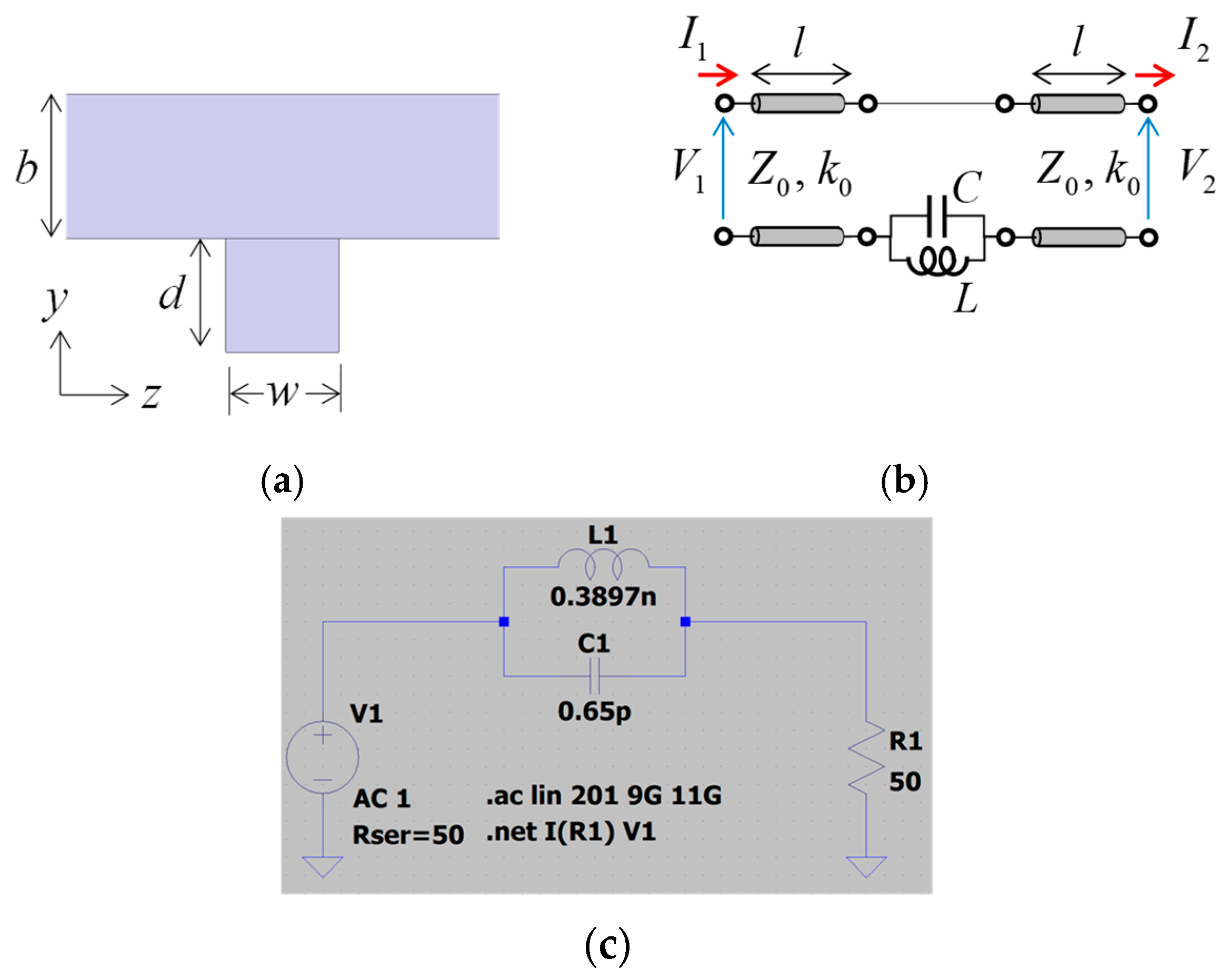
An E-plane terminated short-circuit stub with BSF characteristics (Figure 4a) can be simply represented by a series connection of an LC parallel resonant circuit (Figure 4b). Figure 4c shows the circuit simulation model of a single stub. Analog Devices LTspice [33,34] was used as the circuit simulator. Since the characteristic impedance of waveguides is not uniquely determined, the source impedance and load impedance are assumed to be 50 Ω, and the phase of the S-parameters is not used. Therefore, the input transmission line and output transmission line of length l included in the EM simulation model in Figure 1 are omitted. The procedure for extracting the equivalent circuit element values is as follows. First, |S11| near the resonant frequency f0 is calculated using EM simulation. Then, the value of C or L in the LC equivalent circuit is changed using circuit simulation to search for the element values that give the closest |S11|. Since the resonant frequency f0 is known, once the value of either LC is determined, the other is automatically determined by Equation (1).
f 0 = 1 2 π L C
In extracting element values, the search is performed under the condition that the residual sum of squares average Sr, defined by Equation (2), is minimized.
S r = 1 N i = 1 N S 11 CS ( f i ) S 11 EM ( f i ) 2
where the residual is the difference between the reflection coefficient |S11| of circuit simulation (CS) and EM simulation. fi (i = 1, 2, …, N) is the frequency sample. Although it is possible to use |S21|, which has sharp resonance characteristics, a slight mismatch between the resonant frequencies of CS and EM increases the residual error near the resonant frequency, so |S11|, which has dull resonance characteristics, was used.
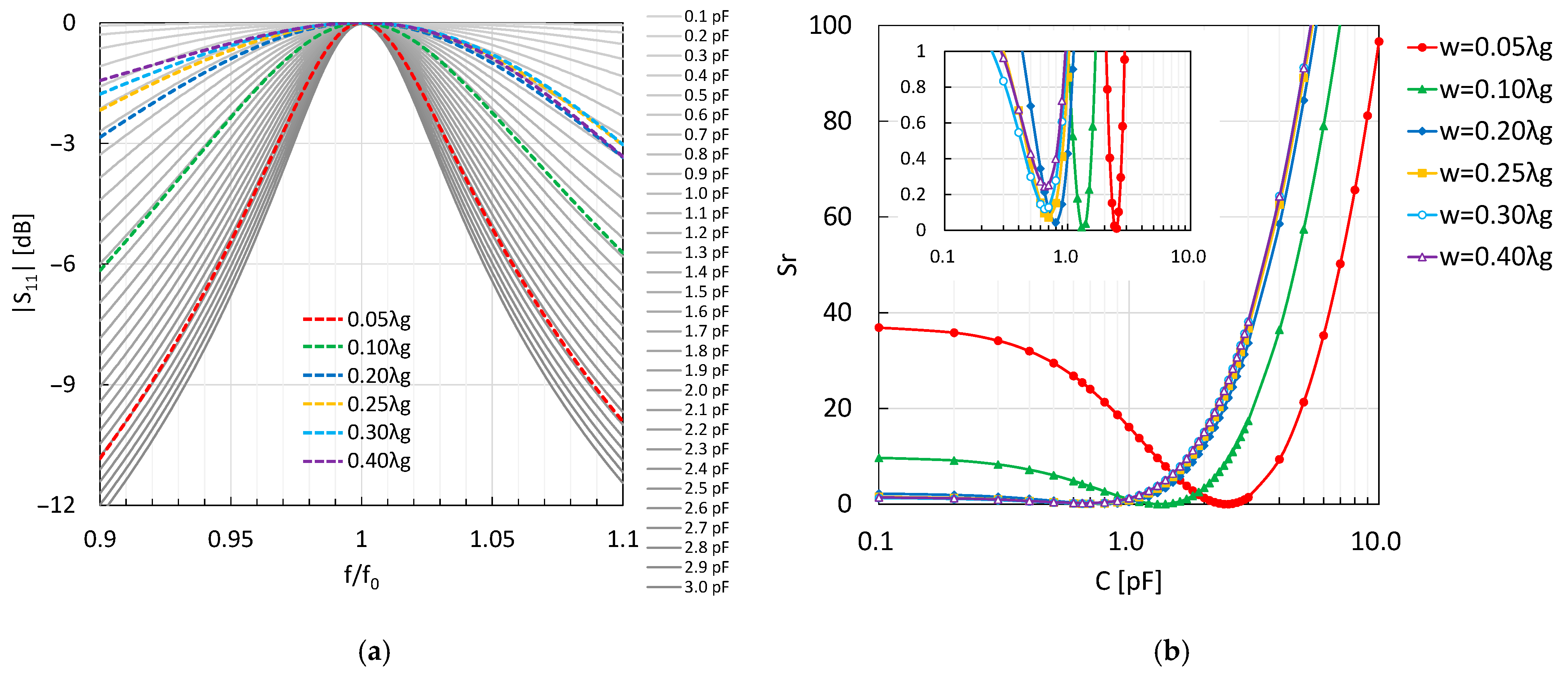
Figure 5a shows the |S11| characteristics calculated by EM simulation for six stub widths (w = 0.05 λg to 0.40 λg) superimposed on the |S11| characteristics calculated by circuit simulation (in gray). The circuit simulation displays results in increments of 0.1 pF up to 3.0 pF. The two do not match perfectly, but it is possible to extract the circuit element values that minimize the residual error. Figure 5b shows the change in residual error Sr calculated from Equation (2) versus capacitance C. The six legends indicate the differences in width w. As width increases, the value of capacitance C, at which Sr is minimized, tends to decrease. This tendency is physically correct. An enlarged view of Sr is shown in the upper left of the figure. At w = 0.30 λg and w = 0.40 λg, the value of C that minimizes Sr remains unchanged, but the minimum value rises slightly. This shows that a simple LC parallel resonant circuit is not sufficient due to the influence of higher order modes. However, there is a value of C that minimizes Sr, so we will adopt this as the equivalent circuit element value. This is very useful for later theoretical analysis.
Table 2 summarizes the results of extracting the equivalent circuit element values of the EM simulation data by |S11| fitting using an LC parallel resonant circuit. The table shows the stub depth d, capacitance C, inductance L, reactance XC, XL, and normalized reactance xC, xL by 50 Ω for six stub widths (w = 0.05 λg to 0.40 λg). From these results, the widening of the stopband by the single stub is achieved by increasing the reactance of the equivalent circuit. For this type of equivalent circuit analysis, an equivalent circuit model using the variational method has been proposed by Marcuvitz [35], but its scope of application is limited to standard structures that can be calculated theoretically. In contrast, in this research, it is possible to match LC circuit element values to the physical shape of a resonator of any shape, and if the equivalent circuit is appropriately determined, it is a highly versatile method. Once the values of the equivalent circuit elements in a single stub are determined, the attenuation characteristics for any number of cascaded stages can be calculated approximately without relying on costly EM simulations, using either circuit simulations or Floquet’s theorem [36,37,38,39,40,41]. This calculation determines the minimum number of cascade stages required to meet the specifications. To determine the optimal period spacing, it is necessary to define an appropriate objective function and perform iterative calculations using optimization methods such as genetic algorithms or gradient descent methods. This study does not employ optimization techniques. Instead, it focuses on the mechanism of spurious passbands and quantitatively demonstrates that the cascade spacing that prevents spurious passbands across the widest bandwidth is an odd multiple of λg/4 later on.

3. Characteristics of Two-Stage Cascaded Stub

3.1. Cascade Characteristics

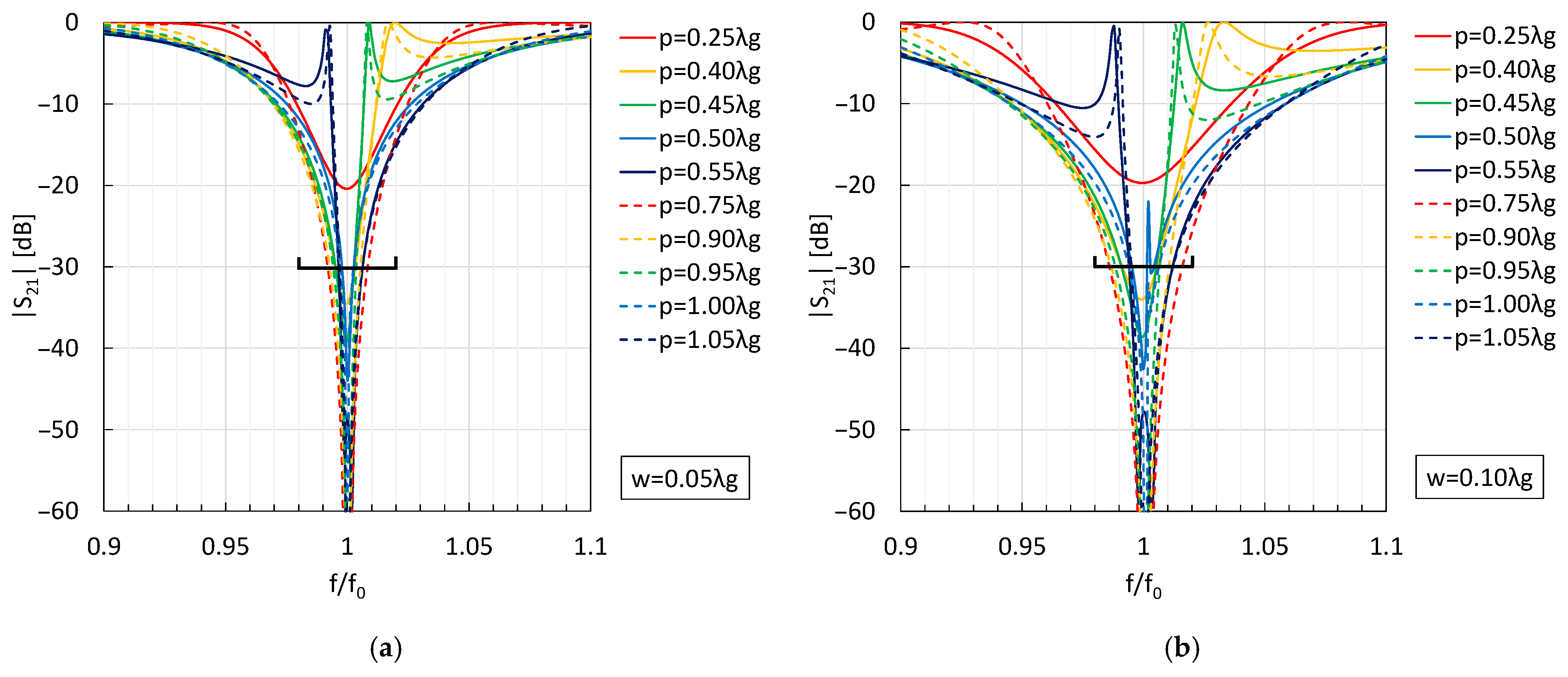
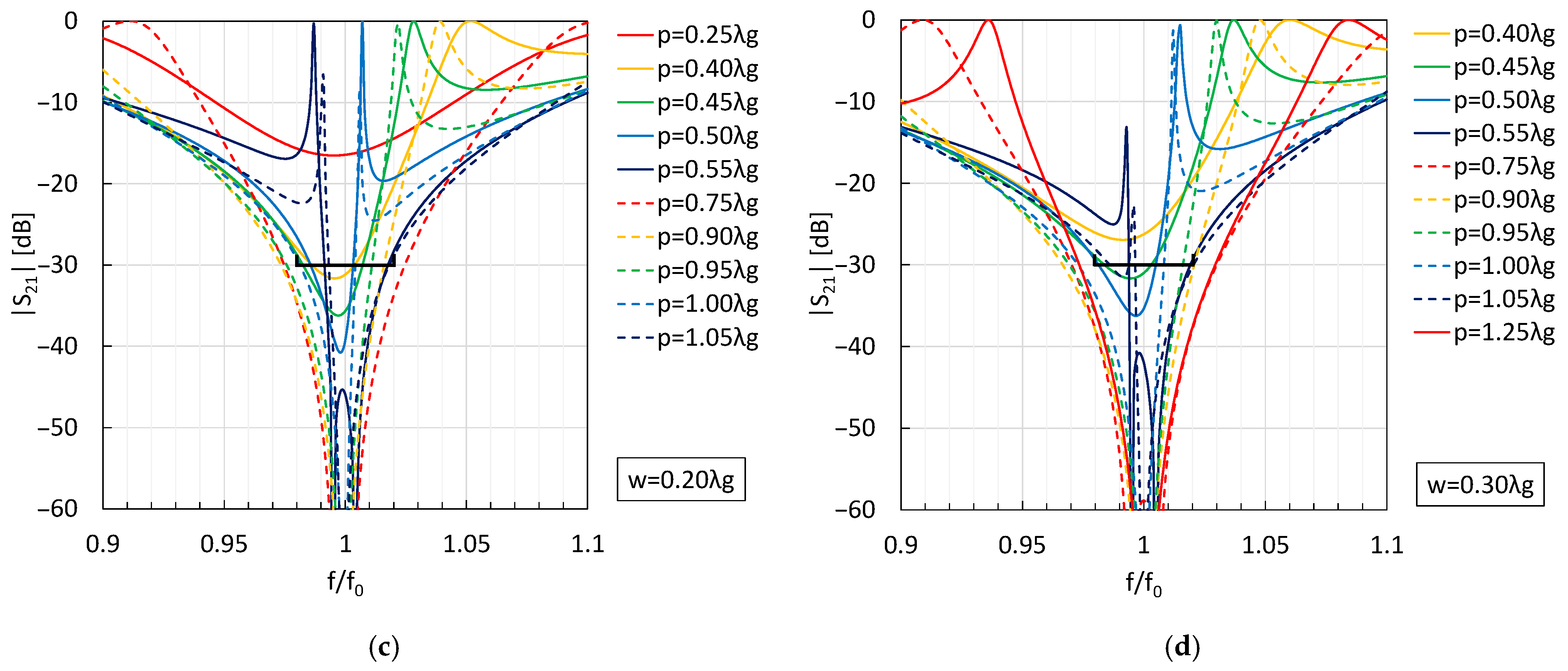
In Chapter 2, we showed that increasing the width of a single stub widens the stopband characteristics, because the reactance of the LC parallel equivalent circuit increases. However, a single stub could not satisfy the required rejection characteristics of |S21| ≤ −30 dB and FBW = 4%. To widen the stopband width, it is necessary to increase the number of stages, and empirically, the most commonly used cascade spacing is λg/4. This value is used for periodic structures to represent EBG or metamaterials, but it cannot be applied to wider stubs with w > λg/4. In two-stage stub configurations, cascade spacing p critically affects performance by influencing spurious passband generation. EM simulations for stub widths w = 0.05 λg to 0.30 λg (Figure 6) show that wider stubs expand the stopband, but certain spacings introduce spurious passbands. For example, spurious passbands appear near p = 0.50 λg and 1.00 λg. When p is half a wavelength longer, similar spurious characteristics arise due to periodicity.

3.2. Spurious Generation Mechanism

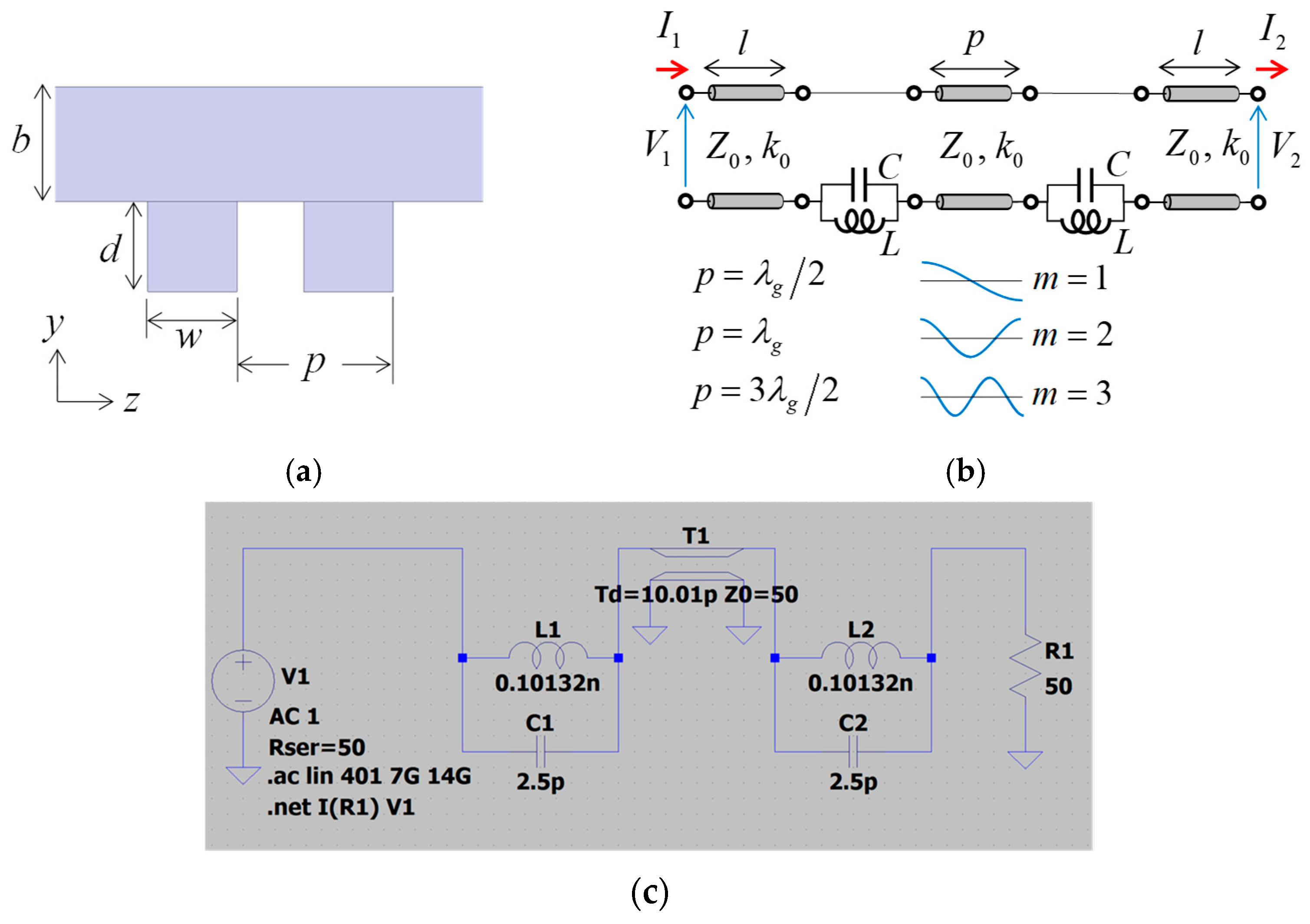
In this section, we will investigate the cause of spurious passbands occurring within the stopband. The cause of the spurious frequency can be discussed by comparing with equivalent circuit analysis. Figure 7 shows the EM simulation model and equivalent circuit model of the two-stage cascaded stub. When two parallel resonant circuits resonate, the transmission line of length p sandwiched between the two resonant circuits operates as an open-ended resonator. This causes a spurious passband within the stopband. Since this open-ended transmission line resonator resonates at integer multiples of half a wavelength, the resonance conditions are expressed by p = mg/2), (m = 1, 2, 3, …). Figure 7b shows the spurious resonance modes up to m = 3. The reactance of the parallel resonant circuits at both ends of the transmission line exhibits frequency characteristics, causing the spurious frequencies to deviate slightly from the half-wave resonance of the transmission line. There is another resonant mode that generates spurious passbands. When the length p of the open-ended transmission line is much shorter than λg/2, the transmission line does not resonate, but the parallel resonant circuits at both ends can resonate in antiphase. This causes another spurious passband. We define this as the zeroth-order spurious resonant mode (m = 0). In the EM simulation model of Figure 7a, this spurious mode corresponds to the case where the physical length satisfies the condition 2d + p ≃ λg/2. In the circuit simulation (Figure 7c), element values of the LC parallel circuit are selected from Table 2. The cascaded stub spacing p is entered as the transmission line delay time Td in Equation (3), where vp is the phase velocity of the TE10 mode, given by Equation (4).
T d = p v p
v p = ω β = ω k 2 k c 2
In Equation (4), ω is the angular frequency, k is the wave number in free space, and kc is the cutoff wave number of the TE10 mode (kc = π/a). The characteristic impedance Z0 of the connecting transmission line is assumed to be 50 Ω.
Figure 7. Simulation models of two-stage cascaded stub: (a) Side view of the EM simulation model; (b) Equivalent circuit simulation model and image of spurious resonance modes (m = 1, 2, 3); (c) Simulation model of two-stage cascaded stub by LTspice.
Electronics 14 04660 g007
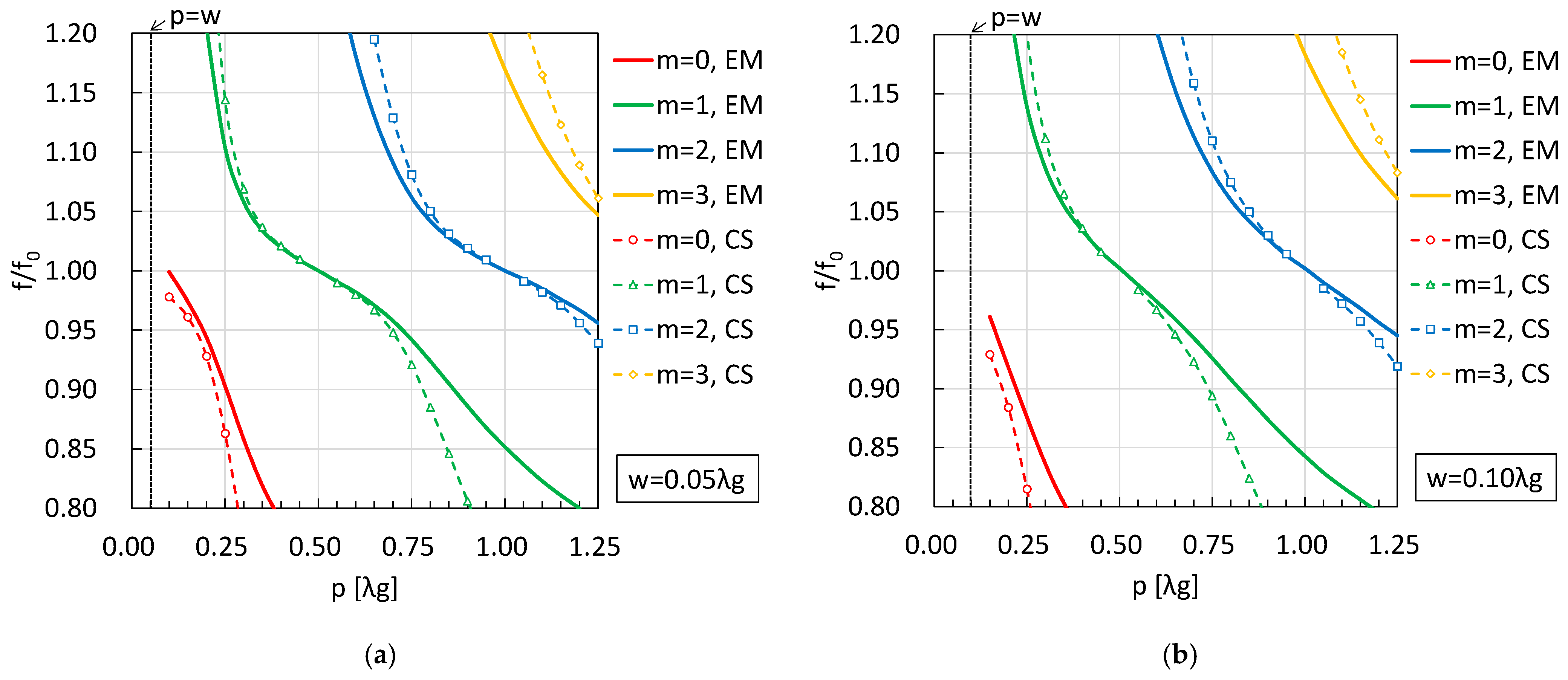
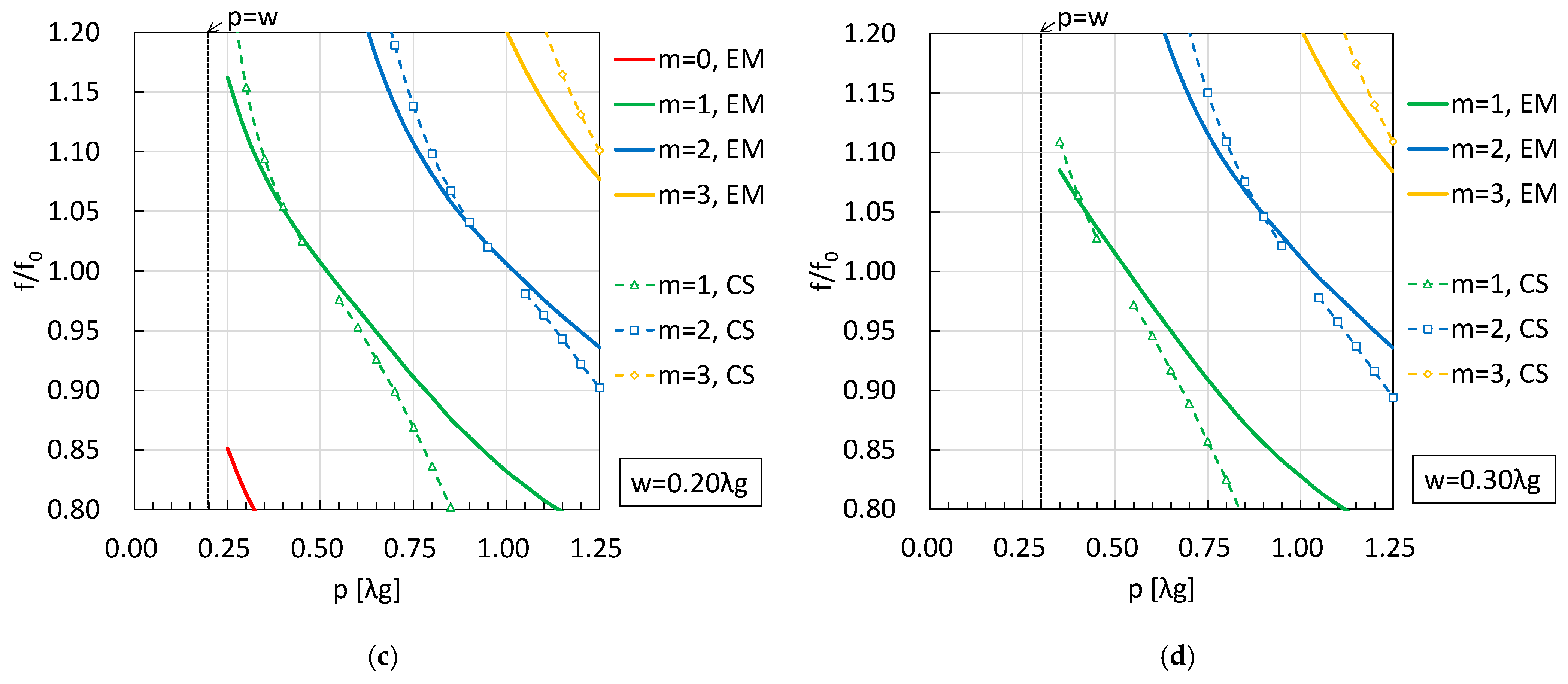
Figure 8 shows the relationship between the cascade spacing p and the spurious frequency. The legend indicates spurious resonance modes (m = 0 to 3). The solid lines show the spurious frequencies obtained from the EM simulation in Figure 6 and dashed lines with markers show the ones obtained from the circuit simulation. The region to the left of the perpendicular dashed line drawn at position p = w has no physical meaning, so no simulation data exists.
Two calculation results are in good agreement around f/f0 = 1.00. In the circuit simulation, spurious frequencies are not observed (no markers) only when f/f0 = 1.00. This is because the attenuation of parallel resonant circuits in circuit simulation is theoretically infinite, thereby canceling out the spurious passband. When p = 0.25 λgg/4), the stopband width is widest, centered around f/f0 = 1.00 in all cases except for Figure 8d (w > λg/4). This coincides with the periodicity interval most used in EBG and metamaterial.
When p = 0.75 λg (3 λg/4), the stopband width becomes narrower than when p = λg/4, but another stopband centered at f/f0 = 1.00 is generated. Similarly, when p = 1.25 λg (5 λg/4), the stopband width is narrower than when p = 3 λg/4; there is another stopband centered at f/f0 = 1.00. It should be noted that the wider the stub width w, the wider the stopband width centered on f/f0. It was found that the cascade spacing p that generates no spurious modes in the widest band is an odd multiple of λg/4. For wider stubs w > λg/4, it is not possible to use the cascade spacing p = λg/4, but p = 3 λg/4 can be used instead.

4. Multi-Stage Cascaded Stubs

Multi-Stage Characteristics

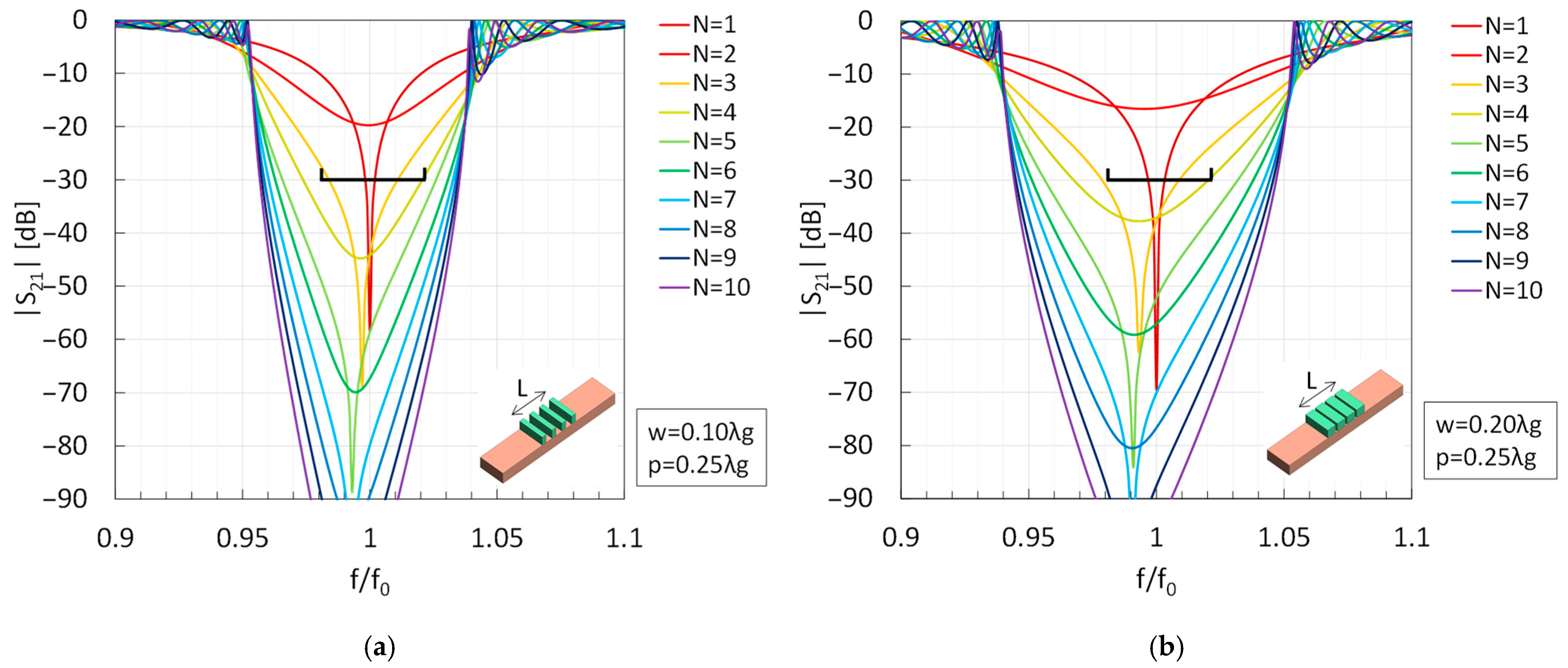
Figure 9 shows the multi-stage characteristics when the cascade spacing is p = λg/4. The horizontal axis shows the normalized frequency, the vertical axis shows |S21|, and the legend indicates the number of cascade stages N. A target line is drawn for the required rejection level |S21| ≤ −30 dB and FBW = 4%. Two results are shown for w = 0.10 λg and 0.20 λg, where the required specifications can be achieved by increasing the number of stages. In both cases (a) and (b), the required specifications can be achieved with N = 4. A general view of the filter is shown in the lower right of the figure. If the minimum number of cascade stages that meets the required specifications is Nmin, the minimum filter size is given by L = w + p(Nmin − 1). Therefore, excluding the connecting waveguides at both ends (l = 2 λg), the filter size of (a) is L = 0.85 λg and the filter size of (b) is L = 0.95 λg.
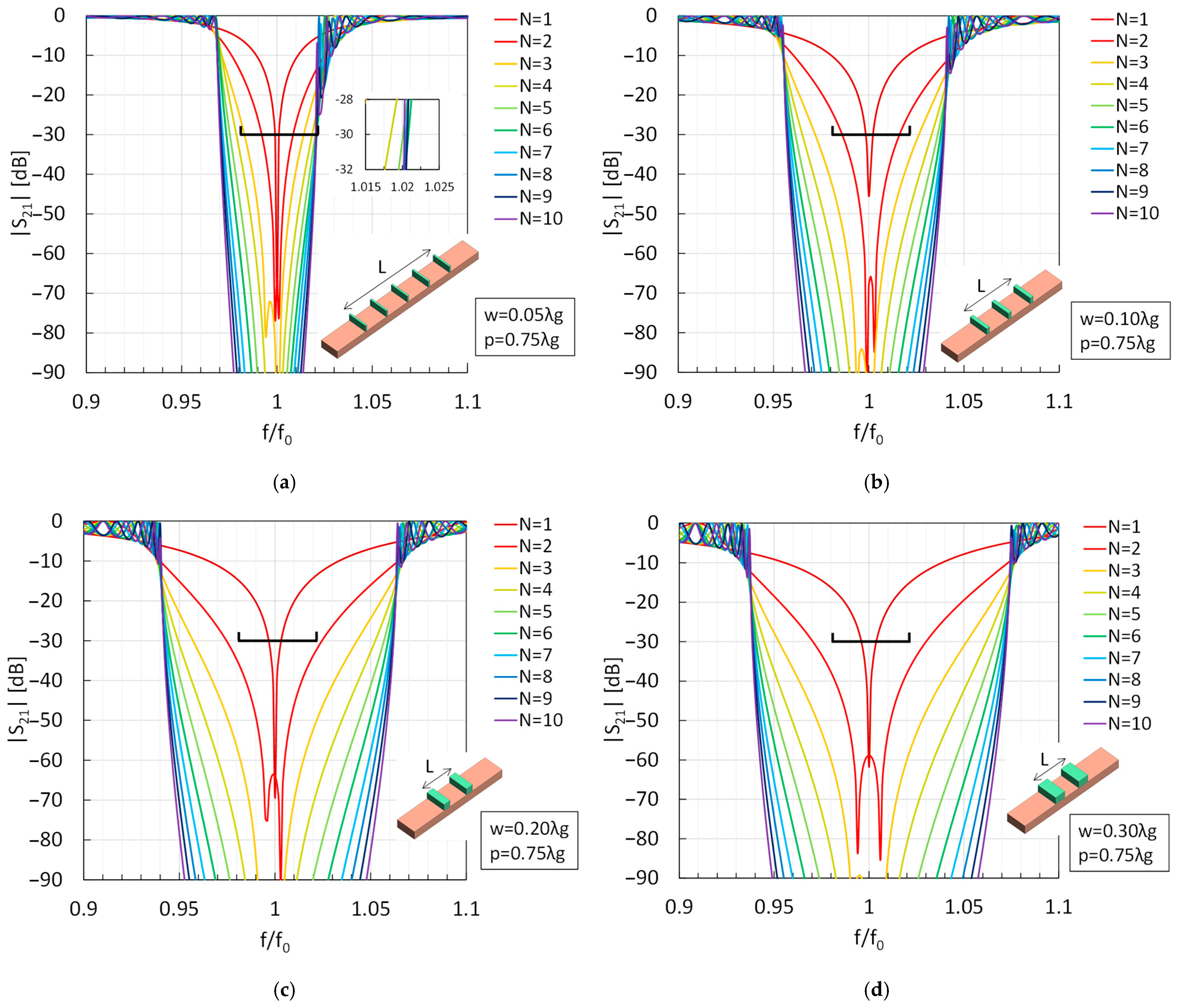
Figure 10 shows the multi-stage characteristics when the cascade spacing is p = 3 λg/4 and the number of stages is changed. The horizontal axis shows the normalized frequency, the vertical axis shows |S21|, and the legend indicates the number of cascade stages (N = 1 to 10). The target line is drawn for the required rejection level |S21| ≤ −30 dB and FBW = 4%. Four results are shown for w = 0.05 λg to 0.30 λg, where the required specifications can be achieved by increasing the number of stages. In case (a), the required specifications can be achieved with Nmin = 5, and the minimum filter size is L = 3.05 λg. The figure shows critical areas enlarged. When the cascade spacing p = λg/4 and the stub width w = 0.05 λg, the required specifications could not be achieved even with N = 10 (this is not shown in Figure 9). In case (b), Nmin = 3, and the minimum filter size becomes L = 1.6 λg. Compared to Figure 9a, which uses the same stub width w = 0.10 λg and the cascade spacing of λg/4, the filter size increases by a factor of 1.9. However, it is noteworthy that the attenuation level at the center frequency improves from –45 dB to −85 dB. In case (c), Nmin = 2 and minimum filter size is L = 0.95 λg. Compared with Figure 9b, where the same stub width w = 0.20 λg and the cascade spacing is p = λg/4, the filter size is the same, and the rejection level at the center frequency is improved from −37 dB to −64 dB. This indicates that there is a great advantage in reducing the number of resonators and increasing the cascade spacing. The findings may have applications in other filter designs or array antennas with finite periodicity. In case (d), Nmin = 2 and the minimum filter size is L = 1.05 λg. Since w > λg/4, a comparison with the case where the cascade spacing is p = λg/4 is not possible, but the filter size is almost the same as in (c), and improvements can be seen in the stopband width. As reported in [6,7], significant interaction between the fringing fields around the apertures of the closely spaced stubs can greatly affect the bandstop performances. Thus, p = λg/4 may not be a practical design for the studied waveguide bandstop structure. However, when p = 3 λg/4, the structure is analogous to the waveguide bandstop filter presented in [6,7].
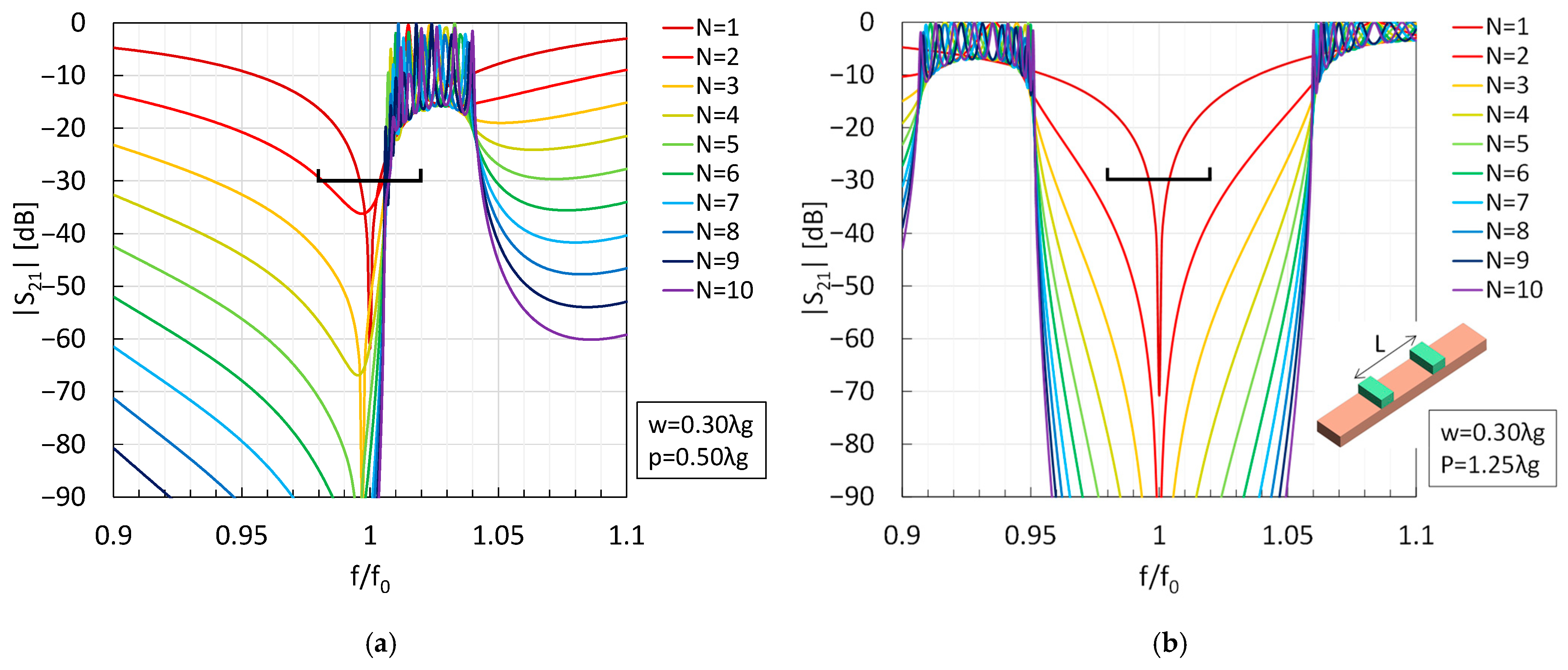
To validate the odd-multiple hypothesis, wider stub width w = 0.3 λg with different cascade spacings (p = λg/2 and 5 λg/4) were investigated. Figure 11 shows the results. The horizontal axis shows normalized frequency, the vertical axis shows |S21|, and the legend indicates the number of cascade stages (N = 1 to 10). The target line is drawn for the required rejection level |S21| ≤ –30 dB and FBW = 4%. Two results are shown for p = λg/2 and 5 λg/4. In case (a), it is not possible to meet the required specifications. In case (b), the required specification is achieved with Nmin = 2, and the minimum filter size is L = 1.55 λg. Compared to Figure 10d for the same stub width w = 0.30 λg with p = 3 λg/4, the stopband width has decreased by 7%, and the filter size has increased by 48%. Therefore, p = 5 λg/4 may not be a practical design period.

5. Experimental Validation and Measurement Results

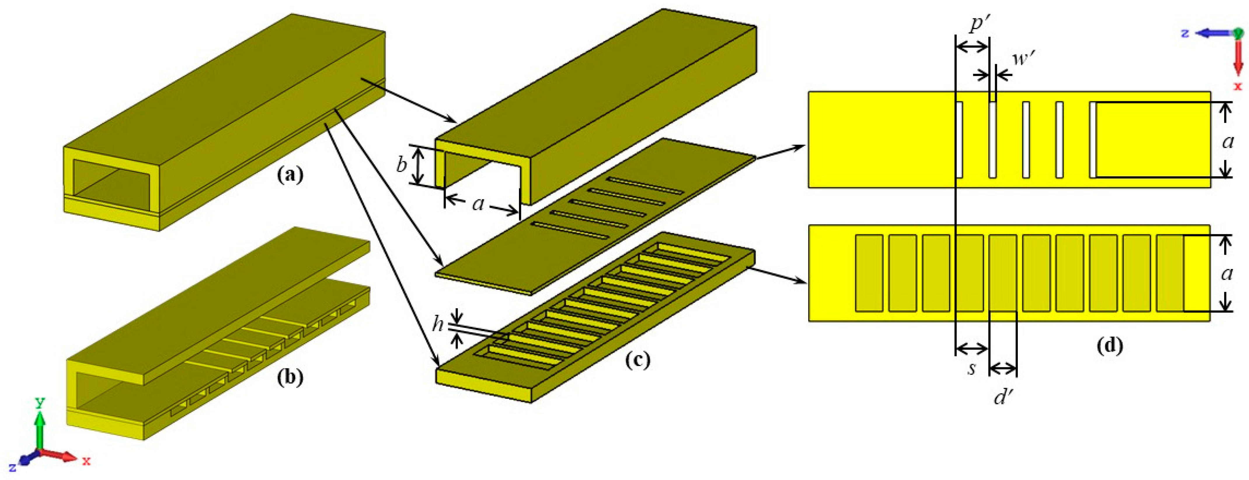
To allow for experimental verification, we designed a WR90 waveguide periodically loaded with E-plane bent stubs. Figure 12 illustrates the structural descriptions and physical realization of the presented measurement design. The test fixture consists of three main components: the top cover, middle plate, and bottom base. The top cover is designed to meet the standard WR90 (a = 22.86 mm and b = 10.16 mm) waveguide specifications. The middle plate contains coupling slots strategically aligned with the rectangular cabinets on the bottom base to control wave coupling effectively, and each coupling slot had dimensions of 22.86 mm (length, a) by 2 mm (slot width, w’). The bottom base contains multiple rectangular cabinets arranged periodically, each with dimensions of a = 22.86 mm, the width of the cabinets d’ = 8.2 mm and the depth of the cabinets h = 2 mm. The spacing between adjacent cabinets was set to approximately s = 0.25 λg, equivalent to 10 mm at the targeted frequency, ensuring resonance control and effective suppression characteristics. All three components were custom fabricated to form a robust and flexible experimental platform. It is noticed that the spacing between adjacent slots on the middle plate p’ is designed as an integer multiple of s. Since s = λg/4, the periodicity of the fabricated rectangular waveguide with stub structures can be configured as an integer multiple of λg/4, by appropriately designing the middle plates. Both the number of periods and the periodicity are thus controlled by virtue of tailored middle plate design. Such a reconfigurable test fixture would make the measurement flexible and cost-effective.
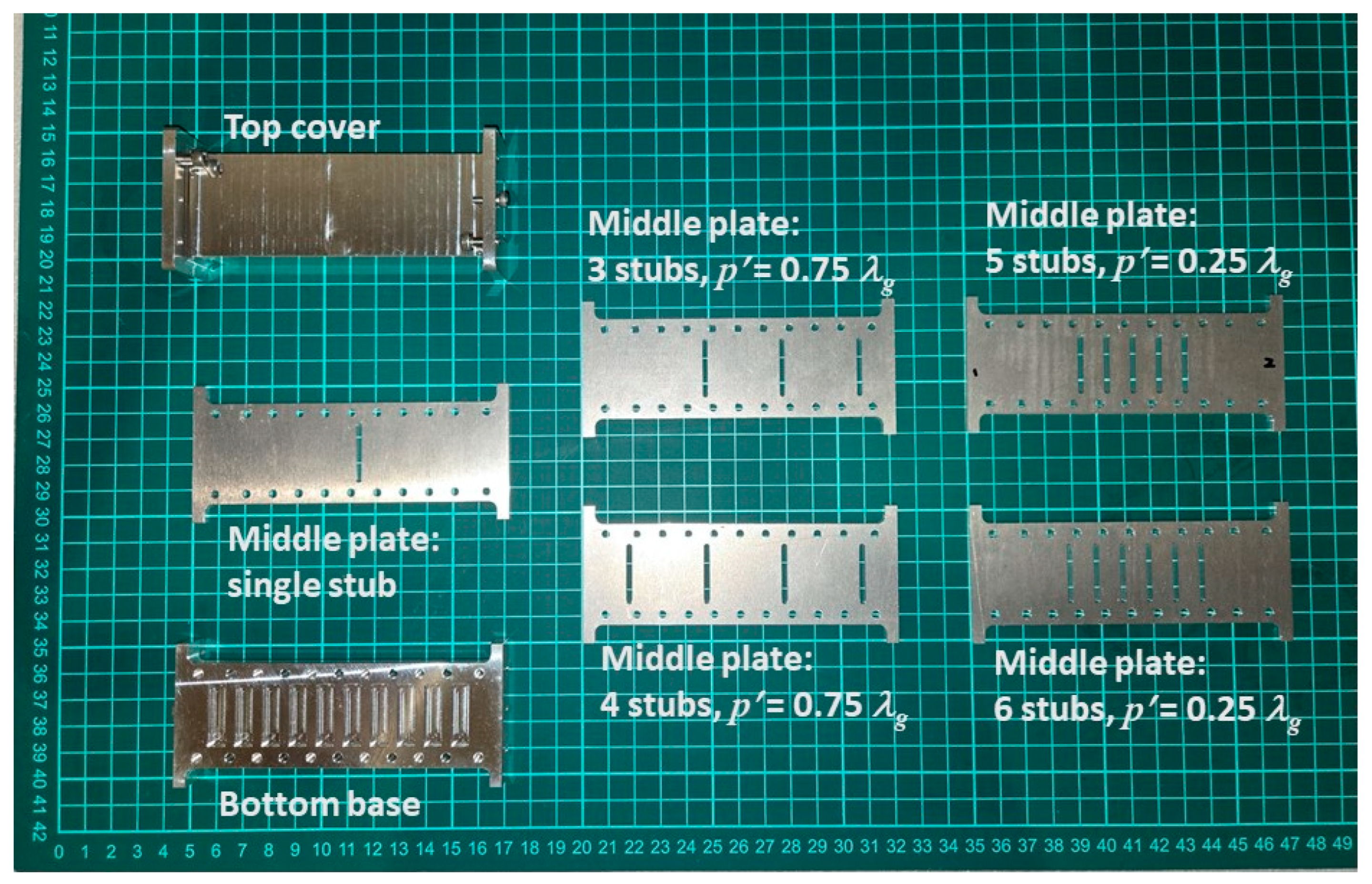
Figure 13 shows the fabricated components of these test samples. All these implementations were based on a bent stub configuration, which significantly reduces the overall circuit size while preserving the same electrical performance.
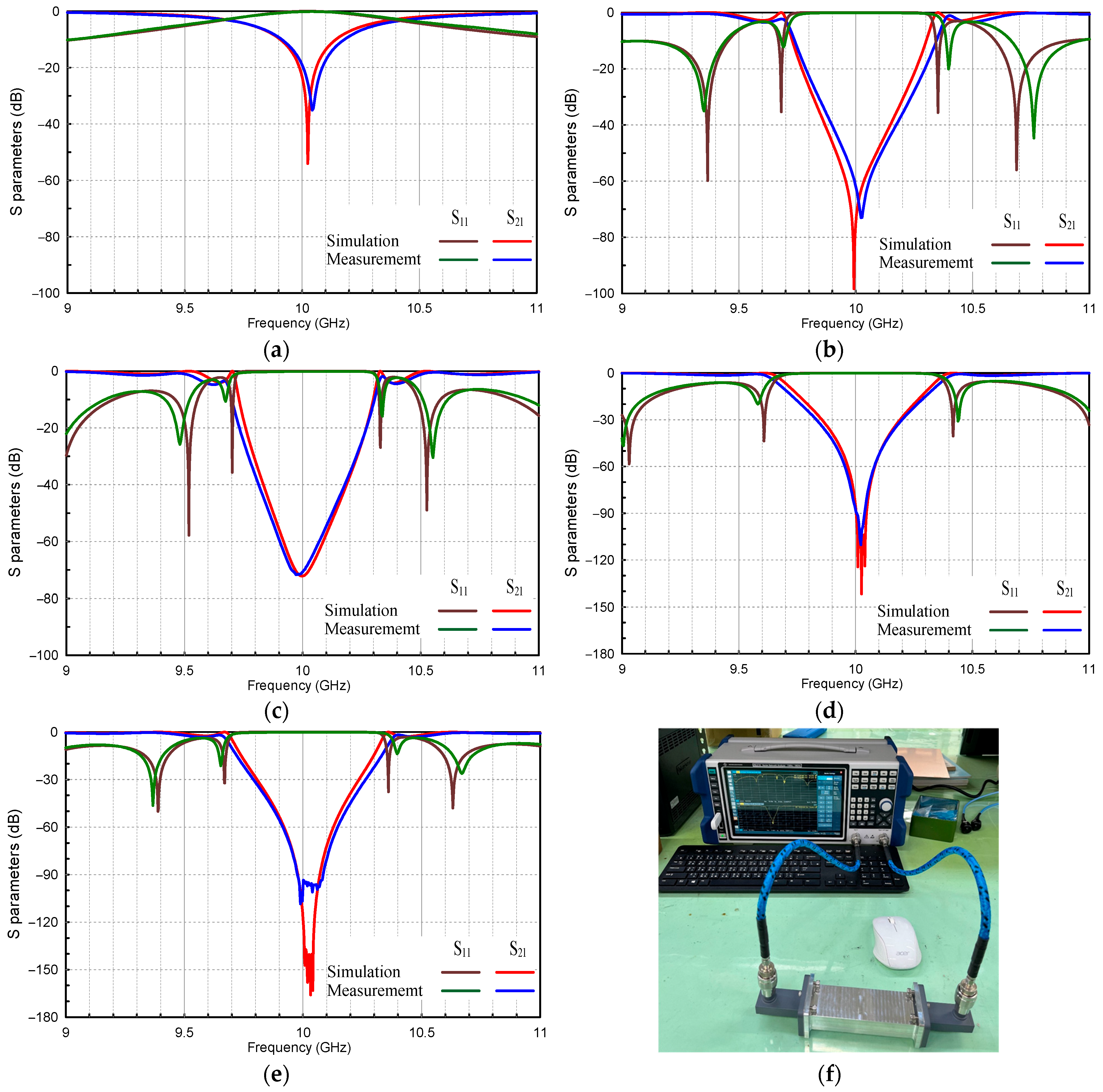
We examined five configurations to evaluate the filter’s performance under varying stub counts and periodic spacings (Figure 14): a single stub (baseline), two cases with five and six stubs at p’ = λg/4, and two cases with three and four stubs at p’ = 3 λg/4. Configurations Figure 14d,e correspond to N = 3 and N = 4 in Figure 10a.
Measurement results from the five experimental setups demonstrated excellent consistency with simulated data. The measurement results matched closely with the predicted results, confirming the theoretical predictions regarding the filter’s performance. Specifically, the results clearly show the effectiveness of the periodic stub spacing and the E-plane stub configuration in suppressing unwanted spurious passbands while maintaining robust bandstop characteristics. Thus, these measurements substantiate our original theoretical models and validate the practical applicability of the proposed design.

6. Summary

This study explored the design of a waveguide bandstop filter using a finite periodic structure of identically shaped stubs to suppress electromagnetic wave leakage in continuous microwave heating processes. Emphasis was placed on the influence of stub width, which governs the stopband bandwidth, and cascade spacing, which affects the emergence of spurious passbands. The key findings are as follows: Increasing the stub width broadens the stopband width. Wide stubs are beneficial for achieving a wider stopband when cascading multiple stages. On the other hand, stub depth does not affect the stopband width but facilitates control of the resonant frequency. Spurious passbands occur due to half-wavelength resonance, either between closely coupled stubs or within the transmission line between resonators. The optimal cascade spacing to suppress spurious passbands across the widest bandwidth is an odd multiple of λg/4. For a wider stub width greater than λg/4, 3 λg/4 spacing is particularly effective in bandwidth and rejection level improvement. Reducing the number of resonators and increasing the cascade spacing is a great advantage in terms of reducing manufacturing costs and improving attenuation. Experimental validation using a configurable WR90 test fixture demonstrated strong agreement with simulation results and confirmed the practical efficacy of the proposed design.
These conclusions provide a foundation for the systematic design of compact and efficient bandstop filters for leakage suppression in microwave heating and related applications. The proposed design method can be applied to other waveguide standards without compromising its versatility, as it allows dimensions normalized at wavelength λg to be replaced with dimensions for any frequency band of interest. However, in this study, the WR90 standard waveguide was adopted to facilitate experimental verification. Developing evaluation methods for multimode waveguides with widths and heights different from the standard waveguide remains a future research topic.

Author Contributions

Conceptualization, Y.K. and H.-H.C.; methodology, Y.K. and H.-H.C.; software, Y.K. and K.M.; validation, Y.K., H.-H.C. and Y.-W.H.; formal analysis, Y.K., K.M. and H.-H.C.; investigation, Y.K., H.-H.C., Y.-W.H. and K.M.; resources, Y.K. and H.-H.C.; data curation, Y.K. and H.-H.C.; writing—original draft preparation, Y.K., H.-H.C., Y.-W.H., R.W.J. and K.M.; writing—review and editing, Y.K., H.-H.C., Y.-W.H. and R.W.J.; visualization, Y.K., H.-H.C. and Y.-W.H.; supervision, Y.K.; project administration, Y.K.; funding acquisition, Y.K. and H.-H.C. All authors have read and agreed to the published version of the manuscript.

Funding

This work was supported by JSPS KAKENHI Grant Number 24K07461.

Data Availability Statement

The original contributions presented in the study are included in the article, further inquiries can be directed to the corresponding author.

Conflicts of Interest

The funders had no role in the design of the study; in the collection, analyses, or interpretation of data; in the writing of the manuscript; or in the decision to publish the results.

References

  1. Iwabuchi, K.; Fukai, I.; Kashiwa, T. Consumer Applications of Microwaves: Microwave Ovens and Accessories. In Handbook of Microwave Technology; Ishii, T.K., Ed.; Academic Press: San Diego, CA, USA, 1995; Volume 2, pp. 249–275. [Google Scholar]
  2. Kim, E.; Kim, B.; Nam, S. Analysis of electromagnetic wave transmission through a choke using FE-BIM with arbitrary incident angle/polarization. IEEE Trans. Electromagn. Compat. 1997, 39, 11. [Google Scholar] [CrossRef]
  3. Pyne, B.; Naruse, R.; Saito, H.; Hirokawa, J.; Ravindra, V.; Akbar, P.R. Robust Contactless Noncircular Choke Flange for Wideband Waveguide Applications. IEEE Trans. Microw. Theory Tech. 2019, 67, 861–867. [Google Scholar] [CrossRef]
  4. Yagitani, S.; Katsuda, K.; Nojima, M.; Yoshimura, Y.; Sugiura, H. Imaging Radio-Frequency Power Distributions by an EBG Absorber. IEICE Trans. Commun. 2011, E94-B, 2306–2315. [Google Scholar] [CrossRef]
  5. Li, Y.; Jin, Y.; Raza, H.; Wang, Y.; Chen, Q.; Zou, X.; Ren, Z.; Guo, J.; Zheng, G.; Cheng, J. Dual driving strategy from micro-polarization to macroscopic conductance: Tailoring optimized low-frequency and wide-band microwave absorption in high-entropy oxides. J. Mater. Sci. Technol. 2025, 235, 110–121. [Google Scholar] [CrossRef]
  6. Matthaei, G.L.; Young, L.; Jones, E.M.T. Microwave Filters, Impedance-Matching Networks, and Coupling Structures; Artech House: Norwood, MA, USA, 1980; pp. 725–773. [Google Scholar]
  7. Cameron, R.J.; Kudsia, C.M.; Mansour, R.R. Microwave Filters for Communication Systems: Fundamentals, Design, and Applications; Wiley: Hoboken, NJ, USA, 2018; pp. 335–338. [Google Scholar]
  8. Levy, R. Compact waveguide bandstop filters for wide stopbands. In Proceedings of the 2009 IEEE MTT-S International Microwave Symposium Digest, Boston, MA, USA, 7–12 June 2009. [Google Scholar]
  9. Zou, H.; Wu, J.; Zhu, M. Ultra-wide Stopband Waveguide Low-pass Filter Design Based on Asymmetric Inductance Unit Structure. In Proceedings of the 2021 IEEE 3rd International Conference on Circuits and Systems (ICCS), Chengdu, China, 29–31 October 2021. [Google Scholar]
  10. Lin, J.-Y.; Wong, S.-W.; Qian, L.; Wang, Y.; Yang, Y.; Liu, Q.-H. Single and Multiple-Band Bandpass Filters Using Bandstop Resonator Sections. IEEE J. Microw. 2024, 4, 293–302. [Google Scholar] [CrossRef]
  11. Sullca, J.F.V.; Cogollos, S.; Boria, V.E.; Guglielmi, M.; Bastioli, S.; Snyder, R.V. Dual-Reject-Band Filters With Resonant Apertures in Rectangular Waveguide. IEEE Trans. Microw. Theory Tech. 2025, 73, 606–619. [Google Scholar] [CrossRef]
  12. D’Auria, M.; Otter, W.J.; Hazell, J.; Gillatt, B.T.W.; Long-Collins, C.; Ridler, N.M. 3-D Printed Metal-Pipe Rectangular Waveguides. IEEE Trans. Compon. Packag. Manuf. Technol. 2015, 5, 1339–1349. [Google Scholar] [CrossRef]
  13. Massoni, E.; Guareschi, M.; Bozzi, M.; Perregrini, L.; Tamburini, U.A.; Alaimo, G. 3D printing and metalization methodology for high dielectric resonator waveguide microwave filters. In Proceedings of the IEEE MTT-S International Microwave Workshop Series on Advanced Materials and Processes for RF and THz Applications (IMWS-AMP), Pavia, Italy, 20–22 September 2017. [Google Scholar]
  14. Yoneda, S.; Shiraki, Y.; Sasaki, Y.; Miyazaki, C. A Gasket-Free Electromagnetic Shielding Structure for 2.4-GHz and 5-GHz Bands Using Cascaded Dual-Behavior SIW Resonators. IEEE Trans. Electromagn. Compat. 2020, 62, 377–385. [Google Scholar] [CrossRef]
  15. Xu, F.; Wu, K. Guided-wave and leakage characteristics of substrate integrated waveguide. IEEE Trans. Microw. Theory Tech. 2005, 53, 66–73. [Google Scholar] [CrossRef]
  16. VanKoughnett, A.L.; Dunn, J.G. Doubly Corrugated Chokes For Microwave Heating Systems. J. Microw. Power 1973, 8, 101–110. [Google Scholar] [CrossRef]
  17. Iwabuchi, K.; Kubota, T.; Sugaya, Y.; Kashiwa, T.; Itiro, F. Effect of Conductor Losses in New-Structure Filters for Suppressing Microwave Leakage. IEICE Trans. Jpn. Part I Electron. 1992, 75, 179–187. [Google Scholar] [CrossRef]
  18. Soto, P.; Boria, V.E.; Catala-Civera, J.M.; Chouaib, N.; Guglielmi, M.; Gimeno, B. Analysis, Design, and Experimental Verification of Microwave Filters for Safety Issues in Open-Ended Waveguide Systems. IEEE Trans. Microw. Theory Tech. 2000, 48, 2133–2140. [Google Scholar] [CrossRef]
  19. Kildal, P.-S.; Alfonso, E.; Nogueira, A.; Iglesias, E. Local Metamaterial-Based Waveguides in Gaps Between Parallel Metal Plates. IEEE Antennas Wirel. Propag. Lett. 2009, 8, 84–87. [Google Scholar] [CrossRef]
  20. Kirino, H.; Ogawa, K. A 76 GHz Multi-Layered Phased Array Antenna Using a Non-Metal Contact Metamaterial Waveguide. IEEE Trans. Antennas Propag. 2012, 60, 840–853. [Google Scholar] [CrossRef]
  21. Brazález, A.A.; Rajo-Iglesias, E.; Vázquez-Roy, J.L.; Vosoogh, A.; Kildal, P.-S. Design and Validation of Microstrip Gap Waveguides and Their Transitions to Rectangular Waveguide, for Millimeter-Wave Applications. IEEE Trans. Microw. Theory Tech. 2015, 63, 4035–4050. [Google Scholar] [CrossRef]
  22. Kirino, H.; Honda, K.; Li, K.; Ogawa, K. A Waffle-Iron Ridge Guide with Combined Fast- and Slow-Wave Modes for Array Antenna Applications. IEICE Trans. Commun. 2018, 101, 349–356. [Google Scholar] [CrossRef]
  23. Rezaee, M.; Zaman, A.U. Groove Gap Waveguide Filter Based on Horizontally Polarized Resonators for V-Band Applications. IEEE Trans. Microw. Theory Tech. 2020, 68, 2601–2609. [Google Scholar] [CrossRef]
  24. Sievenpiper, D.; Zhang, L.; Broas, R.F.J.; Alexopolous, N.G.; Yablonovitch, E. High-impedance electromagnetic surfaces with a forbidden frequency band. IEEE Trans. Microw. Theory Tech. 1999, 47, 2059–2074. [Google Scholar] [CrossRef]
  25. Abhari, R.; Eleftheriades, G.V. Metallo-dielectric electromagnetic bandgap structures for suppression and isolation of the parallel-plate noise in high-speed circuits. IEEE Trans. Microw. Theory Tech. 2003, 51, 1629–1639. [Google Scholar] [CrossRef]
  26. Mishrikey, M. Analysis and Design of Metamaterials. Ph.D. Thesis, Swiss Federal Institute of Technology, Zurich, Switzerland, 2010. [Google Scholar]
  27. Kawakami, Y.; Hori, T.; Fujimoto, M.; Yamaguchi, R.; Cho, K. Low-Profile Design of Metasurface Considering FSS Filtering Characteristics. IEICE Trans. Commun. 2012, 95, 477–483. [Google Scholar] [CrossRef]
  28. Siegel, P.H. Microwaves Are Everywhere: Ovens: From Magnetrons to Metamaterials. IEEE J. Microw. 2021, 1, 523–531. [Google Scholar] [CrossRef]
  29. Kusama, Y. The Secret of Microwave Oven Doors to Prevent Radio Wave Leakage. In RF World No.51; CQ Publishing: Tokyo, Japan, 2020; pp. 88–96. [Google Scholar]
  30. Kusuma, Y. Simulations related to reducing leakage waves through gaps. In Interference Countermeasures and Future Prospects for Cooperation/Fusion of Wireless Power Transmission and 5G Communication; Hashimoto, O., Ed.; CMC Publishing: Tokyo, Japan, 2023; pp. 134–141. [Google Scholar]
  31. Murayama, K.; Kusama, Y. Experimental Study on Miniaturization of Waveguide E-Plane Stubs by Inserting Capacitive Windows. IEICE Trans. Jpn. Electron. 2024, 107, 17–24. [Google Scholar]
  32. Murata Software Femtet. Available online: https://www.muratasoftware.com/ (accessed on 30 November 2024).
  33. Ghanevati, M. Fundamentals of RF and Microwave Circuit Design: Practical Analysis and Design Tools, 2nd ed.; RFPTA: River Forest, IL, USA, 2019; pp. 45–47. [Google Scholar]
  34. S-Parameters with LTspice. Available online: https://wireless-square.com/2016/11/01/s-parameters-with-ltspice/ (accessed on 30 November 2024).
  35. Marcuvitz, N. Waveguide Handbook; Peter Peregrinus: London, UK, 1986; pp. 336–350. [Google Scholar]
  36. Harvey, A.F. Microwave Engineering; Academic Press: New York, NY, USA, 1963; pp. 435–495. [Google Scholar]
  37. Collin, R.E. Foundations for Microwave Engineering, 2nd ed.; McGraw-Hill: New York, NY, USA, 1992; pp. 550–585. [Google Scholar]
  38. Pozar, D.M. Microwave Engineering, 4th ed.; John Wiley & Sons: Hoboken, NJ, USA, 2012; pp. 381–388. [Google Scholar]
  39. Vale, C.A.W.; Meyer, P.; Palmer, K.D. A design procedure for bandstop filters in waveguides supporting multiple propagating modes. IEEE Trans. Microw. Theory Tech. 2000, 48, 2496–2503. [Google Scholar] [CrossRef]
  40. Lech, R.; Mazur, J. Propagation in rectangular waveguides periodically loaded with cylindrical posts. IEEE Microw. Wirel. Compon. Lett. 2004, 14, 177–179. [Google Scholar] [CrossRef]
  41. Yin, Y.; Zhang, B.; Chen, Q.; Wu, K. Simulation-Assisted Formulas for Propagation Constant in Periodic Structures. IEEE Antennas Wirel. Propag. Lett. 2025, 24, 3659–3663. [Google Scholar] [CrossRef]
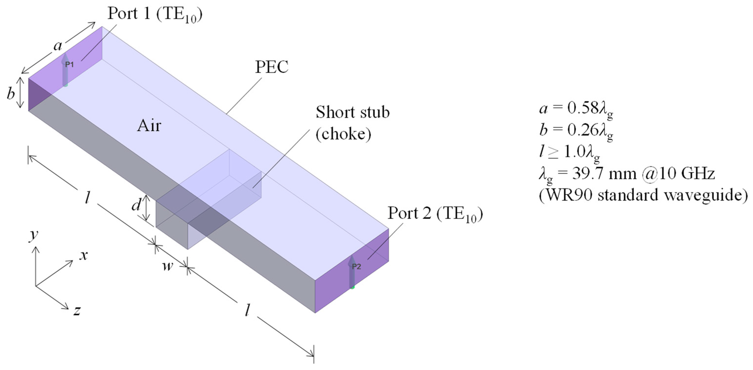
Figure 1. General view of the EM simulation model.
Electronics 14 04660 g001
Figure 2. Parametric sensitivity analysis of a single stub: (a) |S21| characteristics with respect to stub widths w; (b) |S21| characteristics with respect to stub depths d.
Electronics 14 04660 g002
Figure 3. Bandstop characteristics of a single stub with respect to stub widths (w = 0.05 λg to 0.40 λg): (a) |S21| characteristics; (b) |S11| characteristics.
Electronics 14 04660 g003
Figure 4. Single stub simulation model: (a) Side view of the EM simulation model; (b) equivalent circuit model; (c) circuit simulation model using LTspice.
Electronics 14 04660 g004
Figure 5. Fitting of LC parallel resonant circuit element values for a single stub: (a) |S11| characteristics calculated by EM simulation for six stub widths (w = 0.05 λg to 0.40 λg) superimposed on the |S11| characteristics calculated by circuit simulation; (b) change in residual error Sr versus capacitance C.
Electronics 14 04660 g005
Figure 6. EM simulation of two-stage cascade characteristics for different stub widths: (a) w = 0.05 λg; (b) w = 0.10 λg; (c) w = 0.20 λg; (d) w = 0.30 λg; The legend indicates the cascade spacing p.
Electronics 14 04660 g006aElectronics 14 04660 g006b
Figure 8. Relationship between spurious frequency and cascade spacing: (a) w = 0.05 λg; (b) w = 0.10 λg; (c) w = 0.20 λg; (d) w = 0.30 λg; The legend indicates spurious resonant mode (n = 0 to 3).
Electronics 14 04660 g008aElectronics 14 04660 g008b
Figure 9. Multi-stage characteristics when the cascade spacing is p = λg/4: (a) w = 0.10 λg; (b) w = 0.20 λg; The legend indicates the number of stages (N = 1 to 10).
Electronics 14 04660 g009
Figure 10. Multi-stage characteristics when the cascade spacing is p = 3 λg/4: (a) w = 0.05 λg; (b) w = 0.10 λg; (c) w = 0.20 λg; (d) w = 0.30 λg. The legend indicates the number of stages N.
Electronics 14 04660 g010
Figure 11. Multi-stage characteristics of a wider stub (w = 0.30 λg) with different cascade spacings: (a) p = λg/2; (b) p = 5 λg/4. The legends indicate the number of stages N.
Electronics 14 04660 g011
Figure 12. Structural descriptions of the measurement design: (a) Assembled test fixture; (b) Sectional view; (c,d) Exploded view illustrating the detailed dimensions of the top cover, the middle plate featuring coupling windows, and the bottom base containing periodically arranged rectangular cabinets.
Electronics 14 04660 g012
Figure 13. Fabricated components of the test samples, including top cover, bottom base, and various middle plates for different stub configurations.
Electronics 14 04660 g013
Figure 14. Comparison of measured and simulated S-parameter responses for five configurations. The results confirm that the fabricated structures exhibit excellent agreement with EM simulation: (a) single stub; (b) five stubs with p’ = λg/4; (c) six stubs with p’ = λg/4; (d) three stubs with p’ = 3 λg/4; (e) four stubs with p’ = 3 λg/4; (f) measurement setup.
Electronics 14 04660 g014
Table 1. Parameters used in the EM simulation and |S21| ≤ −30 dB bandwidth.
wg]dg]bg]w/bfL/f0fH/f0BWFBW [%]
0.050.21580.260.190.9991.0010.020.2
0.100.20450.260.390.9991.0020.030.3
0.200.20300.260.780.9971.0030.060.6
0.250.20710.260.970.9971.0030.060.6
0.300.21340.261.170.9961.0030.070.7
0.400.23190.261.560.9971.0030.060.6
Table 2. Equivalent circuit element values extracted by |S11| fitting of EM simulation and circuit simulation for six stub widths.
wg]dg]C [pF]L [nH]XC [Ω]XL [Ω]xC [Ω]xL [Ω]
0.050.21582.500.1013−6.3666.366−0.1270.127
0.100.20451.300.1949−12.2412.24−0.2450.245
0.200.20300.800.3166−19.8919.89−0.3980.398
0.250.20710.700.3619−22.7422.74−0.4550.455
0.300.21340.650.3897−24.4924.49−0.4900.490
0.400.23190.650.3897−24.4924.49−0.4900.490
Disclaimer/Publisher’s Note: The statements, opinions and data contained in all publications are solely those of the individual author(s) and contributor(s) and not of MDPI and/or the editor(s). MDPI and/or the editor(s) disclaim responsibility for any injury to people or property resulting from any ideas, methods, instructions or products referred to in the content.