Article

Application and Development of a Double Asymmetric Voltage Modulation on a Resonant Dual Active Bridge

1
Department of Engineering “Enzo Ferrari”, University of Modena and Reggio-Emilia, Via Pietro Vivarelli, 10, 41125 Modena, Italy
2
R&D Department, SiCtech Induction Spain, Rda. de Narcís Monturiol, 5, 46980 Valencia, Spain
3
Energy Department “Galileo Ferraris”, Polytechnic of Turin, 10129 Turin, Italy
4
Department of Electronic Engineering, University of Valencia, Calle Catedrático Agustín Escardino, 9, 46980 Valencia, Spain
*
Author to whom correspondence should be addressed.
Electronics 2025, 14(23), 4625; https://doi.org/10.3390/electronics14234625
Submission received: 23 October 2025 / Revised: 16 November 2025 / Accepted: 20 November 2025 / Published: 25 November 2025

Abstract

The growing market penetration of Electric Vehicles (EVs) requires very efficient bidirectional on-board chargers. These converters must allow the power transfer from the grid to the battery of the vehicle and vice versa, since Vehicle to Grid (V2G) applications enable a mitigation of the peak demand and help regulate both the voltage and the frequency of the grid. In this paper, an innovative double asymmetric modulation was studied and applied to a resonant Dual Active Bridge (DAB), CLLC resonant filter configuration. The results of the study showed a significant efficiency boost and an easier controllability of the converter with respect to more traditional modulations or variable frequency techniques, maintaining Zero-Voltage Switching (ZVS) conditions for all the switches in a wide operating range, from 28 to 100% of the maximum power (4–14 kW). A map of optimum points, where converter losses are minimized, is calculated offline through an algorithm in MATLAB R2024a and a proper interpolation between these points allows any output power for each possible voltage level of the battery to be achieved: from 250 V up to 400 V. The modulations are compared and evaluated through simulations carried out in PLECS, both offline and using hardware-in-the-loop (HIL), as well as through experimental tests.

1. Introduction

Nowadays, the world is pushing towards transportation electrification, especially with utilitarian Electric Vehicles (EVs) being widespread in the market. Of course, in this context, charging stations (and, therefore, battery chargers) are also entering the market, allowing for long trips. On-board chargers are composed of three elements [1]: an EMI filter; an AC/DC converter, which rectifies the grid voltage over a Bus DC, most likely film capacitors; and an efficient bidirectional DC/DC converter that allows the power transfer from the grid to the battery and vice versa in a V2G configuration. Since the need for high efficiency in the DC/DC conversion is trivial, several investigations into the converter topology have been conducted over the years, and several studies have been performed on different modulation techniques. The most common topologies are either DAB or Resonant DAB, since they are suited for achieving ZVS, Zero-Current Switching (ZCS), or, in some cases, both. The ZVS condition is satisfied when the energy stored in the inductance, which is seen by the full-bridge output, is higher than the energy needed to charge and discharge the output capacitances C o s s of the commutation switches during dead-time [2]. As stated by the same authors, an incomplete ZVS, or iZVS, causes non-negligible turn-on losses in the switch and leads to an efficiency drop. The ZCS condition is instead achieved when the device is switched off at zero current. ZCS is generally harder to obtain, and a precise measurement of the current flowing in the resonant tank is needed. In [3], Zero-Voltage Zero-Current Switching (ZVZCS) is achieved in four out of eight switches but requires additional snubber circuits. Moreover, despite being very impressive, this condition is reached for only a small power application. A similar consideration can be made for [4]. For this reason, a more stable and easier to implement ZVS condition is required for all the eight switches of a CLLC resonant DAB, while trying to minimize the total turn-off power losses of the converter; therefore, the condition must aim for, but not reach, a ZCS condition over a wide power range as required by the application. Some papers employed a tunable resonant network or transformer to achieve a wide power range application [5,6,7,8]. The problem with these types of applications is both the architectural complexity and the cost of the magnetic parts. An investigation on the effect of a non-traditional modulation on a resonant series DC/DC converter has been conducted in [9]. A triple-phase shift modulation, briefly described in the next Section and optimized for a DAB converter in [10,11,12], was also adopted for the topology studied in [13,14]. Authors of [13] employed a TPS (triple phase shift) with fixed frequency.
In this paper, a more efficient modulation is proposed with the aim of minimizing the total losses without varying the switching frequency, as in [14,15]. Changing the frequency guarantees high efficiencies as demonstrated in [16,17]; however, without a tunable resonant network, the designer must employ a transformer that is not optimized for every switching frequency in the range of variation. At the same time, given a certain root mean square value (RMS) of the current, the switching losses in the transistors increase. The control of the converter also becomes more complex when using frequency modulation. In [17], the output power is obtained through frequency variation but the hyperbolic law describing the relation is practically hard to replicate. Moreover, a variable switching frequency modulation would require a careful analysis of the transformer losses and would deteriorate Electromagnetic Interference, which implies higher costs for EMI/EMC filters. Several studies on the possible modulation techniques applicable to a DAB already exist in the literature and optimal converter design has already been studied [18]. This paper focuses on a new fixed frequency modulation pattern applied to a Resonant CLLC DAB. The modulation takes inspiration from the Asymmetric Voltage Cancellation (AVC) technique described in [19] for a resonant Full-bridge (FB) converter, extending its application to a resonant DAB, thereby creating a new modulation strategy called Double AVC modulation. This technique was found to be more efficient than the well-known TPS at fixed switching frequency. Specifically, the resonant DAB architecture will be described in Section 2 and the technique in Section 3. In Section 4, the algorithm used to define the optimal operating conditions over the desired power range is described; in Section 5, the simulation results are presented; and in Section 6, the experimental setup and the results of the tests are shown. Finally, conclusions are drawn in Section 7.

2. Resonant DAB Configuration

The CLLC Resonant Dual-Active Bridge studied and employed in this paper is shown in Figure 1.
V p and V s represent the primary and secondary voltage, respectively: the first one represents the rectified grid phase voltage from the AC/DC converter which is omitted in the schematic and the second one represents the battery voltage. S 1 ,   S 2 , S 3 , and S 4 are the switches of the first full-bridge (FB1) and Q 1 ,   Q 2 , Q 3 , and Q 4 are the switches of the second full-bridge (FB2). Regarding the tank topology, a CLLC resonant tank is defined. A conventional LC resonant topology is not suited for the asymmetric modulation presented in the next section, since an asymmetric voltage inevitably leads to a DC current component which could saturate the transformer core. For this reason, the resonant inductance L f and the resonant capacitor C f are split between the two sides of the transformer, to eliminate the continuous component and to allow the power transfer in both directions avoiding the saturation of the transformer. The employed values will be given in Section 5. Having said that, a single equivalent LC tank will be considered in the next section for a more transparent discussion, and the relations between the values are defined in (1) ( L f and C f are defined on the secondary side).
L f = L f 1 n 2 + L f 2 C f = n 2 C f 1 · C f 2 n 2 C f 1 + C f 2  
where n is the transformer ratio. L m of Figure 1 represents the magnetizing inductance of the transformer and both C b u s and C o u t are just DC Bus capacitors. Here, the adopted convention is the most common in the literature: forward power transfer when the battery is charged by the grid and reverse power transfer when the battery injects power into the grid.

3. Modulation Techniques

3.1. Introduction to the Modulation Techniques

As mentioned in Section 1, several modulation techniques are reported in the literature. In this section, an existing technique, TPS modulation, is briefly explained and compared to the proposed asymmetric voltage modulation developed for this resonant DAB. For a deeper understanding of the traditional technique, the authors refer to [10,11,12,13,14,15]. A comparison in terms of simulations will be carried out in Section 5. The following subsection is dedicated to the TPS modulation, which will be considered as the state-of-the-art and will later be compared with the proposed modulation, the double AVC.

3.2. TPS Modulation

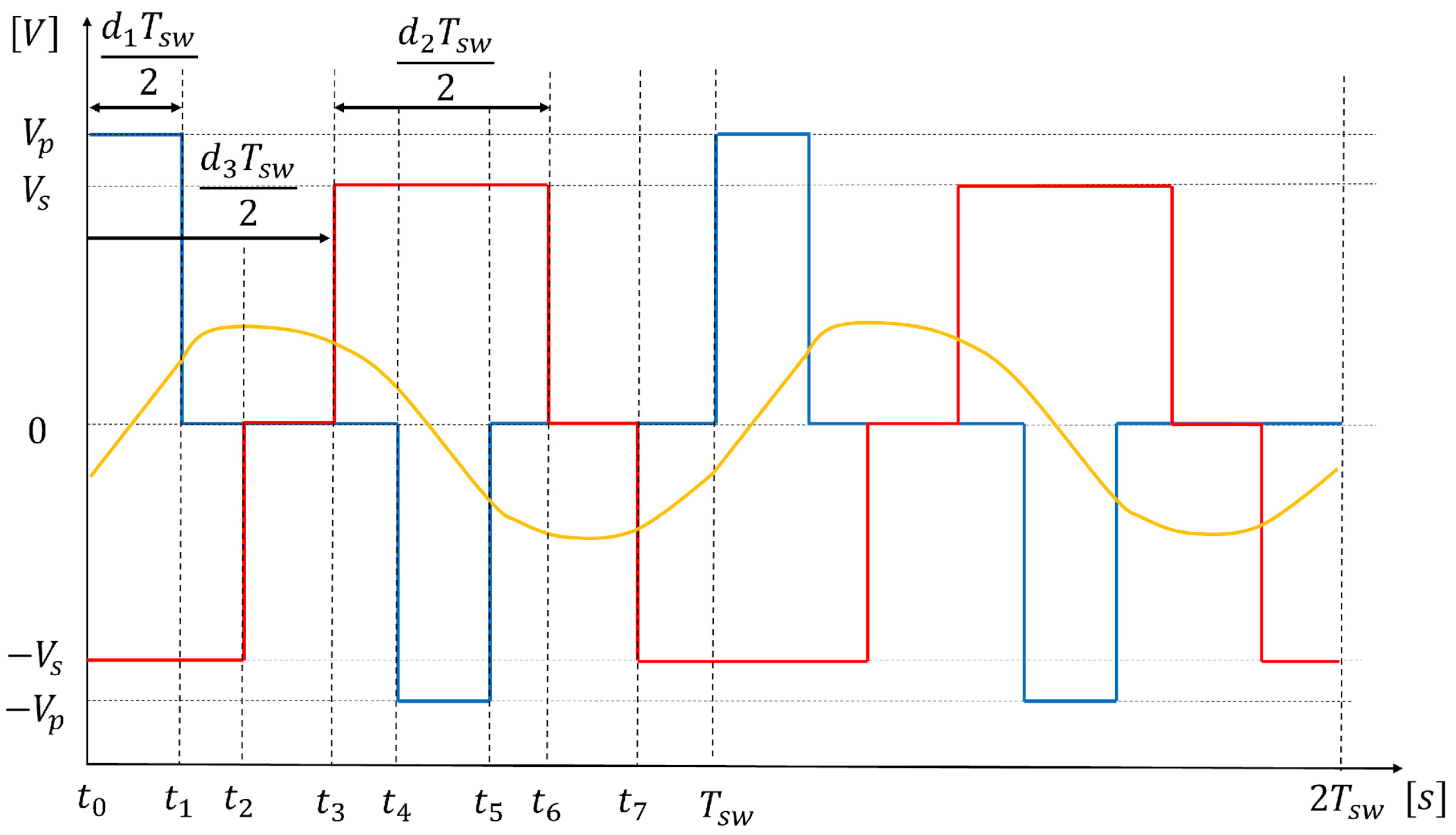
The TPS modulation is a symmetrical modulation applicable to a DAB converter. In [10,11], it was applied to a non-resonant converter and in [12], the TPS modulation was optimized for closed-loop control at a fixed switching frequency f s w . The concept has already been transferred to a series LC resonant DAB in [13,14,15]. Especially in [15], a TPS modulation that minimizes power losses has been developed. TPS modulation includes six possible states, when forward power transfer is considered, from FB1 to FB2, six additional states can be defined for the reverse power transfer and therefore provide significant flexibility. However, as shown in the comparison, the AVC modulation applied to the resonant DAB guarantees higher performance, due to the lower tank current, and at the same time, lower currents during turn-off in the whole power range. Different from [12], the shift from one state to the other, for both TPS and AVC modulation, is dictated by the algorithm described in the next section. The choice has been made to have a fair comparison between the two modulations. As shown in Table 1, the difference between one mode and another depends on the relation between the three variables, or degree of freedom, d 1 , d 2 , and d 3 . Modes are selected based on the relation between duties, which depends on the demanded power [12]; therefore, every time interval cannot be negative. Their meaning is explained in Figure 2: d 1 represents FB1 duty-cycle, d 2 FB2 duty-cycle, and d 3 the internal phase shift between the two bridges. It is sufficient to multiply these values by T s w 2 to obtain t 1 , t 2 , and t 3 . t 5 , t 6 , and t 7 are defined from t 1 ,   t 2 , and t 3 by the symmetry of the modulation in the second half of the switching period.
Figure 2 refers to the case V p > V s , when the primary voltage is superior to the secondary voltage. The classification of the modes does not change if the relation is inverted.

3.3. Proposed Double AVC Modulation

The AVC modulation was applied by the authors of [19] to a full-bridge with a series LC resonant tank feeding a resistive load. In this paper, the technique is applied to a resonant DAB. The advantage of applying double AVC modulation to this type of converter is the possibility of obtaining ZVS for all switches over a wide power range while keeping the switching frequency f s w fixed at a value higher than the resonant frequency f r . A fixed switching frequency, in fact, allows the resonant tank to be exploited at the best possible efficiency, near its resonance, and simplifies the converter control as well. Mathematically, the output voltages of FB1 and FB2 can be expressed using Fourier series with an infinite number of harmonics, (2).
v A B t = V A B . 0 + i = 1 a i , p cos ω t + b i , p sin ω t v C D t = V C D . 0 + i = 1 a i , s cos ω t + b i , s sin ω t  
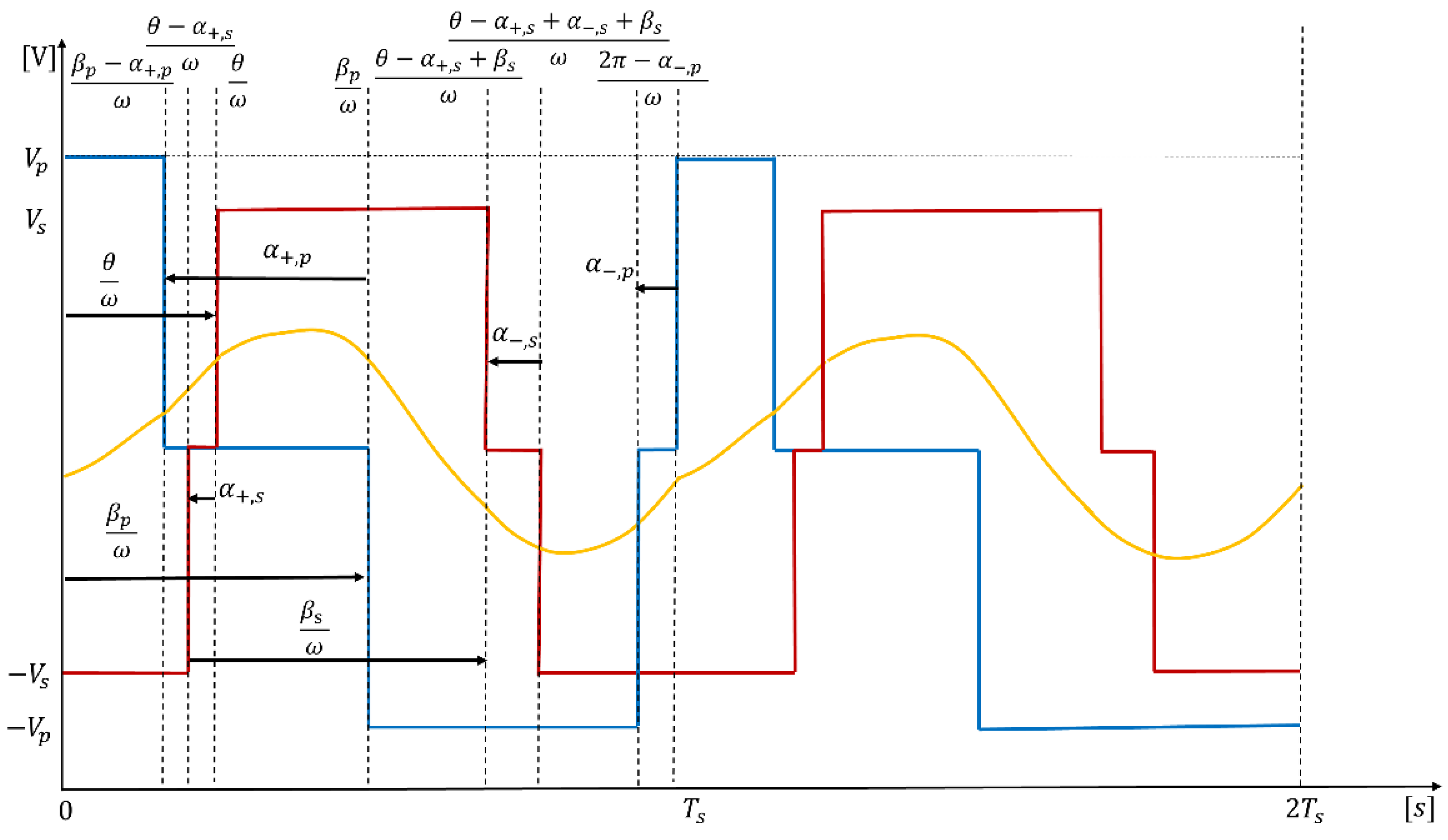
where a i , p , b i , p , a i , s , and b i , s are the Fourier coefficients and V A B . 0 and V C D . 0 are the continuous components of both voltages. In the literature, the most common approach employed to study the CLLC Resonant DAB topology is the FHA, or first harmonic approximation [20], which will be taken into account from now on. Other sophisticated methods, like the State Space Analysis (SPA), already exist in the literature [21], but since the FHA makes it possible to obtain ZVS for each of the eight switches, the over- or underestimation of the losses in a single operating point is considered acceptable. The approximation consists of the omission of the 2nd and 3rd harmonics, which are usually the most significant. Any error introduced by this approximation will be applied to both modulation strategies. Indeed, the aim of this paper is not to provide a detailed and precise description of the converter. Employing the FHA, only four coefficients must be calculated (3)–(6), each corresponding to a coefficient of the Fourier series. Substituting them in (2), the expression in (7) can be found.
a 1 , p = 2 T s · 0 β p α + , p ω   V p cos ω t d t   β p ω 2 π α , p ω V p cos ω t d t  
a 1 , s = 2 T s 0 θ α + , s ω   V s cos ω t d t + θ ω θ + β s α + , s ω V s cos ω t d t θ + β s α + , s + α , s ω 2 π ω V s cos ω t d t  
b 1 , p = 2 T s · 0 β p α + , p ω   V p sin ω t d t β p ω 2 π α , p ω   V p sin ω t d t  
b 1 , s = 2 T s 0 θ α + , s ω   V s sin ω t d t + θ ω θ + β s α + , s ω V s sin ω t d t θ + β s α + , s + α , s ω 2 π ω V s sin ω t d t  
The variables α + , p ,   α , p ,   β p ,   α + , s ,   α , s ,   β s , and θ are explained in Figure 3.
v A B t = V A B . 0 + a 1 , p c o s ( ω t ) + b 1 , p sin ω t v C D t = V C D . 0 + a 1 , s c o s ( ω t ) + b 1 , s sin ω t
The calculation of the two continuous components is not necessary to derive the tank current i x t , since the resonant tank filters out the DC components from both output voltages of the two full-bridges. The expression of I ¯ x , which is the corresponding phasor considering the first harmonic approximation, can be found by considering the system of two equations in (8) and equalizing them (9). Thus, the expression of i x t is obtained in (10).
I ¯ x = V ¯ A B V ¯ p Z ¯ 1 I ¯ x = V ¯ p V ¯ C D Z ¯ 2
I ¯ x = V ¯ A B n V ¯ C D Z ¯ 1 n 2 + Z ¯ 2
i x t = k · b 1 , p n b 1 , s   · cos ω t + a 1 , s a 1 , p n · sin ω t  
where k = ω C f 1 ω 2 L f C f is always negative if the switching frequency is higher than the resonant frequency. This condition also corresponds to the choice made in this paper, since ZVS increases the converter efficiency compared to ZCS. Once the tank current expression is found, its RMS value I x , r m s   , the power output P o , computed as the power absorbed by FB2, and the output current I o can also consequently be derived in (11), (12), and (13).
I x , r m s = 1 2 π 0 2 π i x 2 θ d θ = k   1 2 · b 1 , p n b 1 , s   2 + a 1 , s a 1 , p n 2
P o = 1 2 π 0 2 π v C D θ · i x θ d θ = k 2 · a 1 , s   · b 1 , p n b 1 , s   + b 1 , s · a 1 , s a 1 , p n
I o = k 2 V s · a 1 , s   b 1 , p n b 1 , s   + b 1 , s a 1 , s a 1 , p n
I x , r m s   , P o , and I o depend on k and therefore on the switching frequency and the passive components of the resonant tank, as well as on the set of parameters a 1 , p , b 1 , p , a 1 , s , and b 1 , s . Looking at the expressions in (3)–(6), it is evident that there are seven variables that can be changed to obtain a specific value of the output power P o . The mathematical analysis would become extremely complicated; therefore, some variables are set to constant values, see (14). These simplifications still allow an asymmetrical modulation, while maintaining a symmetrical duty-cycle of 50%. The main advantages of this approach lie in the industrial implementation, both on the optimal points derivation, which does not require a dedicated optimization solver, and on the control of the converter. Under some operating conditions, changing β p and β s could reduce significantly the current of some switches under turn-off, achieving ZVS and ZCS. Seven degrees of freedom modulation would further cut down the switching losses and enhance the efficiency of the converter. Therefore, it represents an interesting solution and, as stated in Section 7, it will be a case-study for a future work. In this paper, α + , p , α + , s , and β s , β p are renamed as shown in (14).
α , p = 0 α , s = 0 β p = β = π β s = β = π α + , p = α p α + , s = α s                
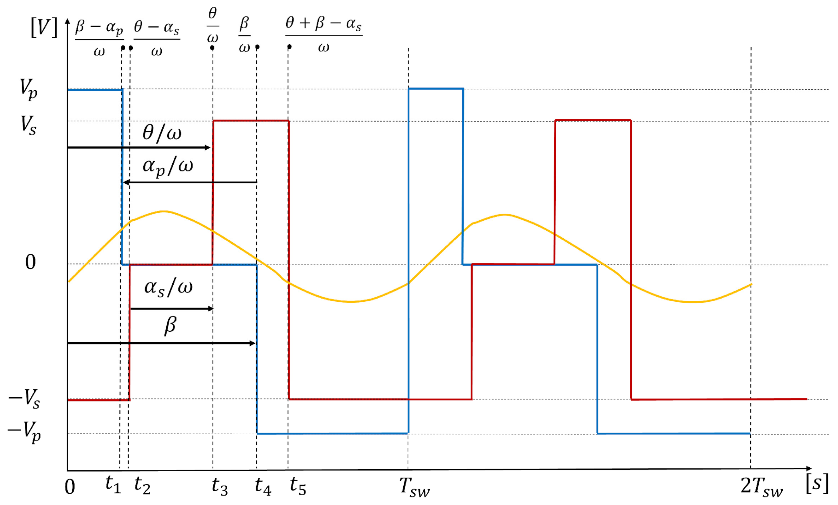
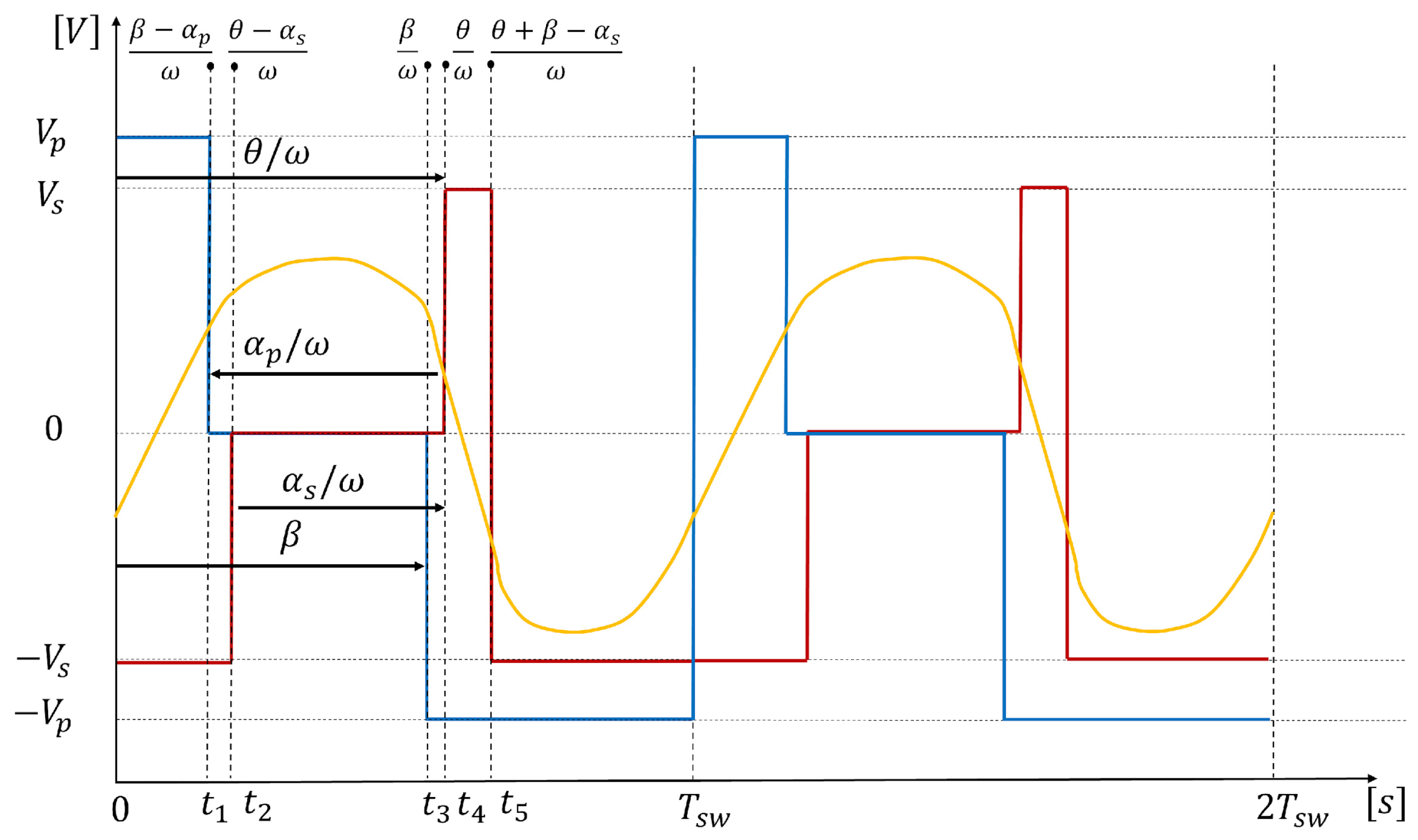
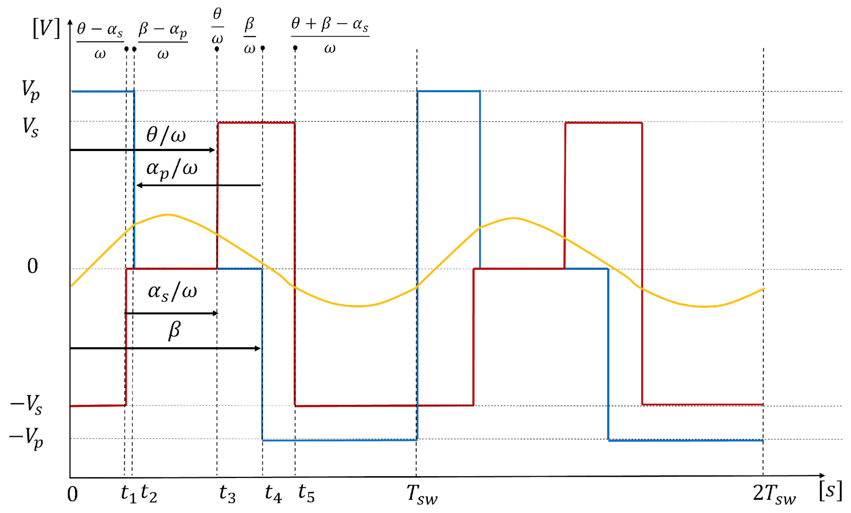
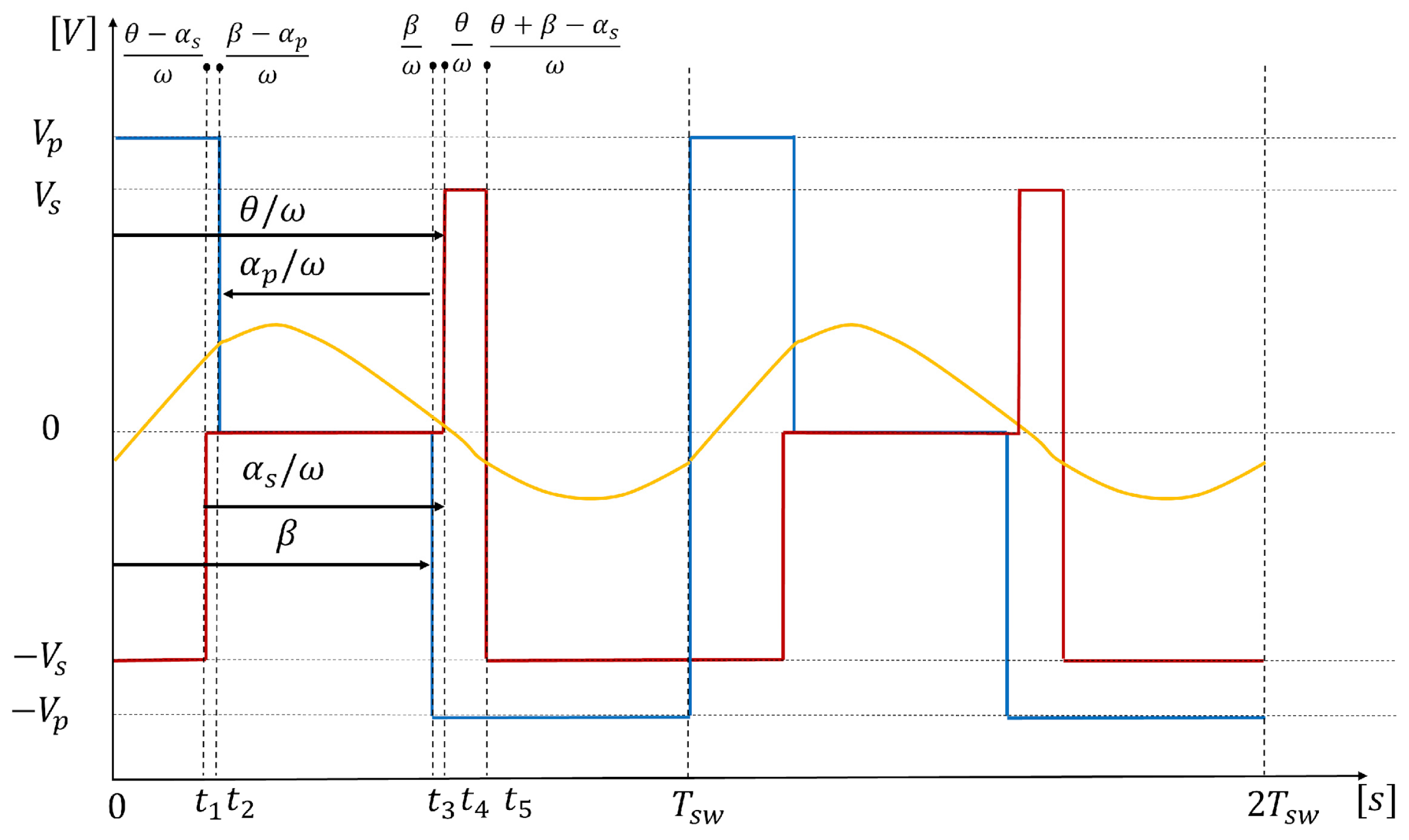
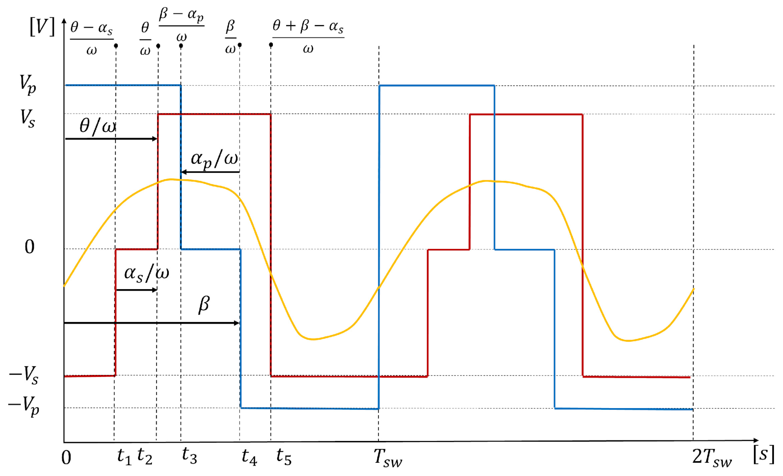
Thus, as for the TPS modulation, several modes can be defined, especially for the double AVC modulation, and five cases can be distinguished: these are summarized in Table 2 and shown in Figure 4, Figure 5, Figure 6, Figure 7 and Figure 8. All figures refer to the case V p > V s , but the classification of the modes does not depend on the voltage levels nor does it change if the relation is inverted. The description of the curves is the same for each figure, and it is provided in Figure 8.
Expressions (10)–(14) will be used in the next section to obtain an optimum array of values of the variable set a 1 , p , b 1 , p , a 1 , s , and b 1 , s that minimizes the sum of the power losses attributable to the transistors, for each value of the requested power P o . The approximate sinusoidal expression of the tank current in (10) is employed to guarantee the ZVS switching condition for each transistor. Expressions (11)–(14) are used for the extraction of the optimal parameters. Sixteen possible sequences are described in Table 3, and each mode is a set of six sequences, which may become five if α p or α s is equal to zero, or four if both are null. In Table 4, modes are associated with their set of sequences when α p =   α s   0 .
There are other possible modes, which are not included in Table 4, but they could not guarantee ZVS for all the eight switches of the converter; therefore, they do not represent a possible outcome of the algorithm described in Section 4.

4. Optimal Operating Conditions and Power Output Control

4.1. Algorithm for Optimal Operating Conditions

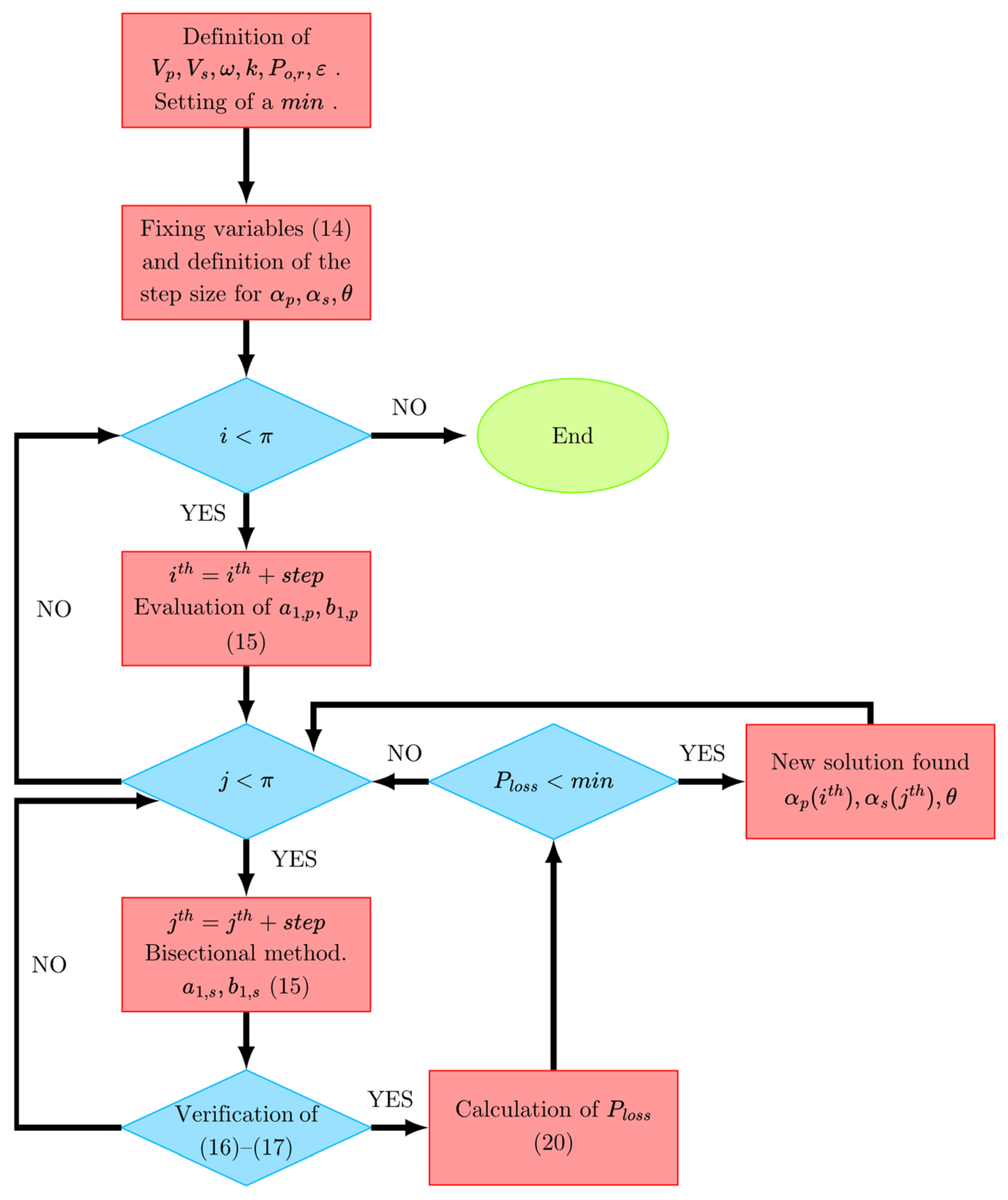
The algorithm employed to find the optimal operating points is implemented in MATLAB, based on a root finding method: the bisectional method, which is very useful to solve systems of non-linear equations. First of all, some variables are fixed to a known value, in this way the number of degrees of freedom can be reduced from seven to three. In fact, in this first work, the authors considered implementing a modulation which does not require any use of non-linear solver. Therefore (14) is used and the expressions of the four coefficients in (3)–(6), become the ones in (15).
a 1 , p = V p π · sin α + , p b 1 , p = V p π · 3 + cos α + , p a 1 , s = V s π · 3 sin θ α + , s sin θ b 1 , s = V s π · 3 cos θ α + , s + cos θ  
Then, values of α + , p and α + , s are swept over the range 0 ;   π within two concatenated for cycles. Finally, for each pair of values α + , p i t h ;   α + , s j t h , where i t h and j t h are the generic iterations of the for cycles, a solution to the problem needs to be found. Here, the bisectional method starts running until a value for θ is found for the aforementioned couple: particularly, substituting the expression in (15) into (12), the value of P o can be evaluated and when the stop condition is satisfied (16), a valid solution is obtained.
P o , r   ε < P o < P o , r   + ε  
where ε is a small error chosen at the start point and P o , r is the requested power. Only if (16) is satisfied, for each given desired power, a value of the triplet α + , p i t h ;   α + , s j t h ; θ is saved, provided that it also allows ZVS for each transistor. The triplet becomes the optimal solution of the problem after all values are swept, if it also minimizes the converter power losses P l o s s , excluding the losses due to the transformer which are hard to estimate offline. The condition of ZVS is represented by the set of equations in (17).
i x , 1 = k b 1 , p n b 1 , s   cos 0 < z i x , 2 = k b 1 , p n b 1 , s   cos θ + a 1 , s a 1 , p n sin θ > z i x , 3 = k b 1 , p n b 1 , s   cos π > z i x , 4 = k b 1 , p n b 1 , s   cos θ + π α + , s + a 1 , s a 1 , p n sin θ + π α + , s < z
where a 1 , p , b 1 , p , a 1 , s , and b 1 , s assume the values in (15). Since the FHA assumes a sinusoidal shape for the tank current and since a non-zero current should circulate in the body-diode to allow the output capacitance to discharge, the value of c must be greater than zero: z > 0 . The variable z also represents a correction factor that accounts for the non-linearities and the higher order harmonics of the tank current, which are not considered in the FHA analysis by definition. This approximation simplifies the mathematical analysis and the algorithm operation significantly. Moreover, the ZVS condition was reached for each switch both in simulation and in the experimental tests over the power range 4–14 kW. Because the predicted power was also close to that calculated theoretically, the FHA has been considered sufficient. From the Fourier spectrum in PLECS, higher order harmonics have also been considered negligible, another proof of the strength of this approximation. P l o s s are instead calculated as the sum of the conduction losses and turn-off losses for every MOSFET. Turn-on losses are neglected since the ZVS condition is imposed. Conduction losses can be estimated through the resistance offered by the MOSFET while conducting R D S , o n , that is provided by the manufacturer. The resultant conduction losses are therefore computed as in (18).
P c o n d , M = R D S , o n · I r m s , M 2
where I r m s , M is the RMS current flowing through the power transistor M during a switching period. The applied formula does not change, but the value of I r m s , M differs from one MOSFET to another. Since for the ZVS conditions, the tank current is considered sinusoidal, the same approximation is perpetuated for the conduction losses calculations. The switching losses, instead, are always determined from the datasheet and, in addition, by assuming independence from the junction temperature since E o f f losses are usually provided for a single temperature value. E o f f losses correspond to the switching losses, and they are evaluated by interpolating the datasheet curve, see (19).
E o f f , M = a · I o f f , M 2 + b · I o f f , M + c
where I o f f , M is the switch-off current of the MOSFET M and a ,   b , and c are the interpolation coefficients. The switching power losses are obtained by multiplying (19) by the switching frequency f s w . As for the conduction losses, the sinusoidal approximation is also considered. The combination of (18) and (19) for each MOSFET returns the total P l o s s (20). The discrimination between two or more possible solutions is based on the minimum value for these losses.
P l o s s = i = 1 4 P c o n d , S i + P o f f , S i + i = 1 4 P c o n d , Q i + P o f f , Q i
For each power level, zero, one, or more solutions are possible. At the end of the algorithm, which is summarized in Figure 9, and for each P o , r   , a ZVS solution that minimizes the power losses is found. The algorithm can be applied to different voltage levels: in this study, the battery voltage changes from a low value, 250 V, discharged battery, to a high value 400 V, charged battery. If P o , r > 0 , the battery is charging, if P o , r < 0 , the battery is discharging, but the algorithm works in the same way. A summary of the algorithm for the optimal operating points is presented in Figure 9. In summary, the algorithm operates in three steps: (i) all the valid triplets α + , p ;   α + , s ;   θ that satisfy P o , r and ZVS constraints, (16) and (17), are found; (ii) P l o s s is calculated for each valid triplet considering switching and conduction losses; and finally, (iii) the triplet that minimizes the losses is selected as the optimal solution.
The algorithm is run offline and the values of α p ,   α s , and θ are saved in three different look-up tables of size v ,   p , where v is the size of the vector V ¯ s = V s , 1 ,   V s , 2 , ,   V s , v and p is the size of the requested power vector P ¯ o , r = P o , r , 1 ,   P o , r , 2 , ,   P o , r , p .

4.2. Control Strategy

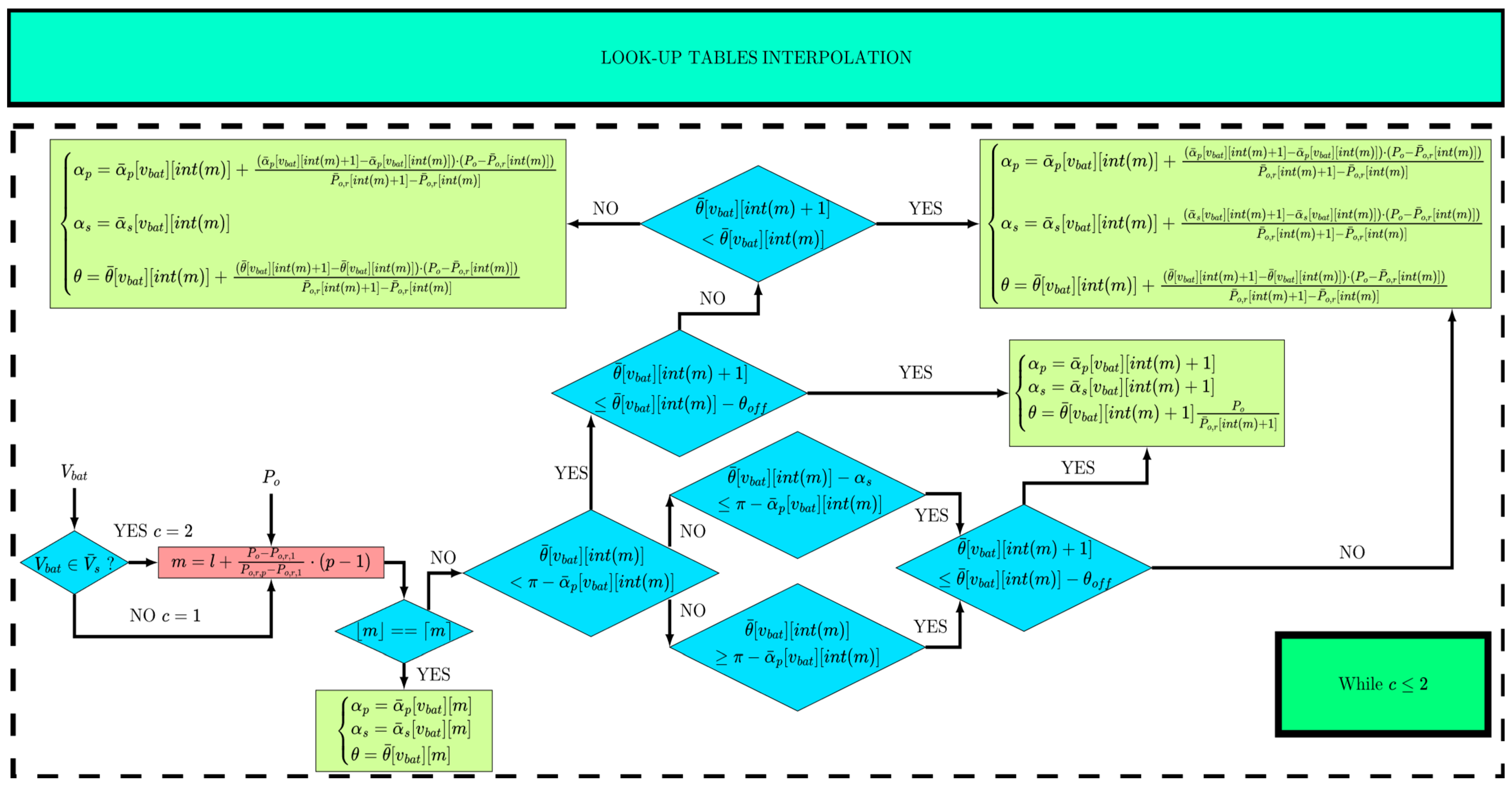
The control strategy presented in this algorithm is based on an appropriate interpolation between the different look-up tables. Since the double AVC modulation can have five different modes that allow ZVS, depending on the mode, one, two, or three look-up tables should be interpolated. The control strategy is therefore summarized in Figure 10 and implemented in a C-script in the simulation.
The main idea behind this control is to obtain any desired power value for any battery voltage on both reverse and forward power transfer, through a selective interpolation of the look-up tables. Figure 10 provides the graphical representation of the code. To further simplify, depending on the mode, a minimum of one and a maximum of three degrees of freedom should be interpolated. θ o f f should be set empirically: the idea consists of modulating only the internal phase shift θ between the two bridges based on the ratio between the desired power P o and the closest greater value of the vector P ¯ o , r . When the value of θ drops from one optimal point to the other in the look-up table, the described strategy is implemented. Instead, if the condition does not occur and the mode is 3 or 4, a full interpolation is performed. The same happens for mode 5, with the exception of θ ¯ v b a t i n t m + 1 < θ ¯ v b a t i n t m : in this case, α s is not interpolated. Consider v b a t :   { V ¯ s v b a t V b a t   &   V ¯ s v b a t + 1 > V b a t } . For the sake of clarity, Figure 10 only shows all the possible look-up table interpolations; however, if V b a t V ¯ s , the interpolation is performed twice and the applied variables become the weighted average of the two solutions α p 1 ,   α p 2 ,     α s 1 ,     α s 2 ,     θ 1 , and θ 2 (21).
α p = α p 1 · V s , v b a t + 1 V b a t V s , v b a t + 1 V s , v b a t + α p 2 · V b a t V s , v b a t V s , v b a t + 1 V s , v b a t α s = α s 1 · V s , v b a t + 1 V b a t V s , v b a t + 1 V s , v b a t + α s 2 · V b a t V s , v b a t V s , v b a t + 1 V s , v b a t θ = θ 1 · V s , v b a t + 1 V b a t V s , v b a t + 1 V s , v b a t + θ 2 · V b a t V s , v b a t V s , v b a t + 1 V s , v b a t
Measuring the battery voltage, the resonant CLLC converter can be precisely controlled through a strategic interpolation of the look-up tables (LUTs). Control can be implemented either on an FPGA or on a commercial microcontroller. A Hardware in the Loop (HIL) simulation in Section 5 demonstrates the statement on an SMT32G474RE microcontroller. In Section 6, experimental tests are instead carried out on real hardware.

5. Simulation Results

This section is divided between an offline simulation, carried out in PLECS, and an HIL simulation, which employs an SMT32G474RE nucleo board and RT Box 3.

5.1. PLECS Offline Simulations

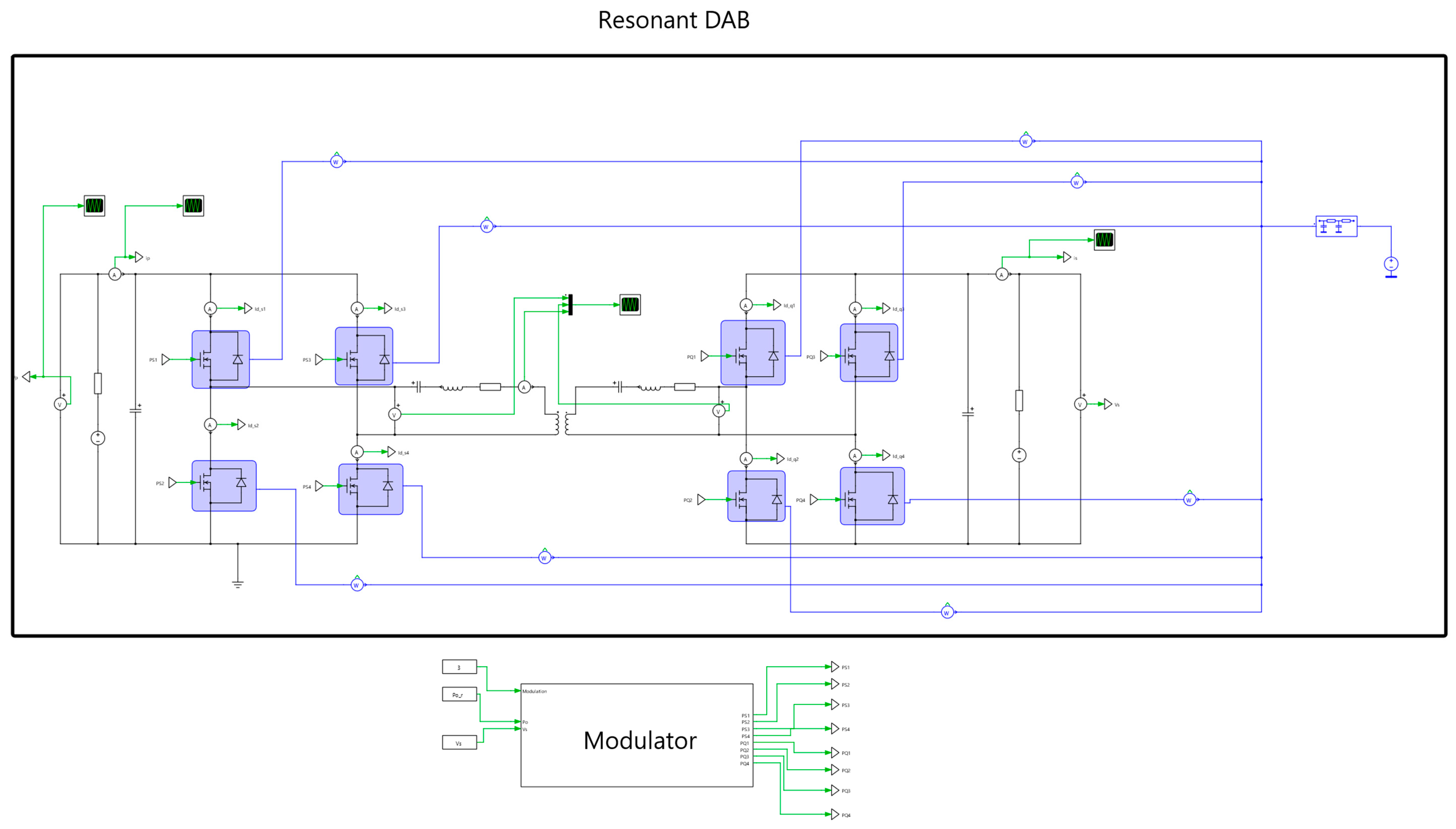
Simulations of the CLLC resonant DAB converter have been carried out in PLECS. In Figure 11, the converter schematic is shown. The “Modulator” subsystem only contains the control strategy explained in the previous section. If modulation = 1 is selected, the AVC modulator is activated; otherwise, if modulation = 2 is selected, the TPS modulation is chosen. The converter parameters are summarized in Table 5: parasitic elements, including transformer ratio and magnetizing inductance, have been chosen based on available passive components. Although not explicitly stated,   L f 1 = L f 2 and C f 1 = C f 2 and the output power range is valid for forward and reverse power transfer.
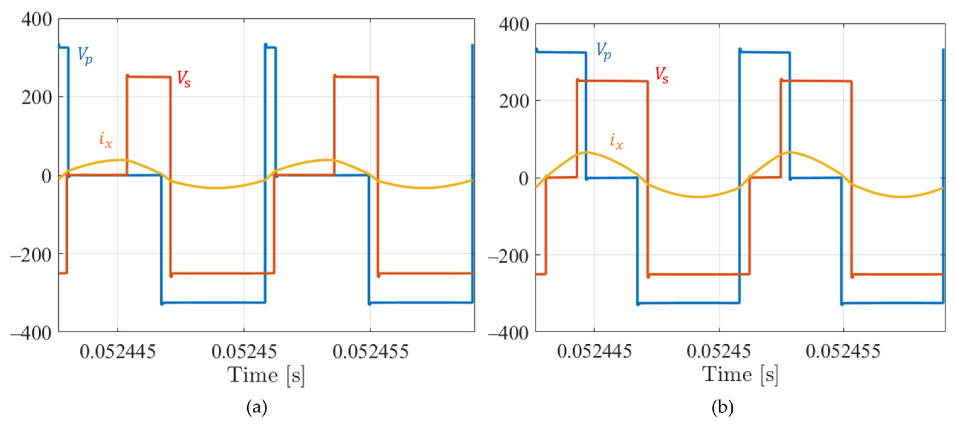
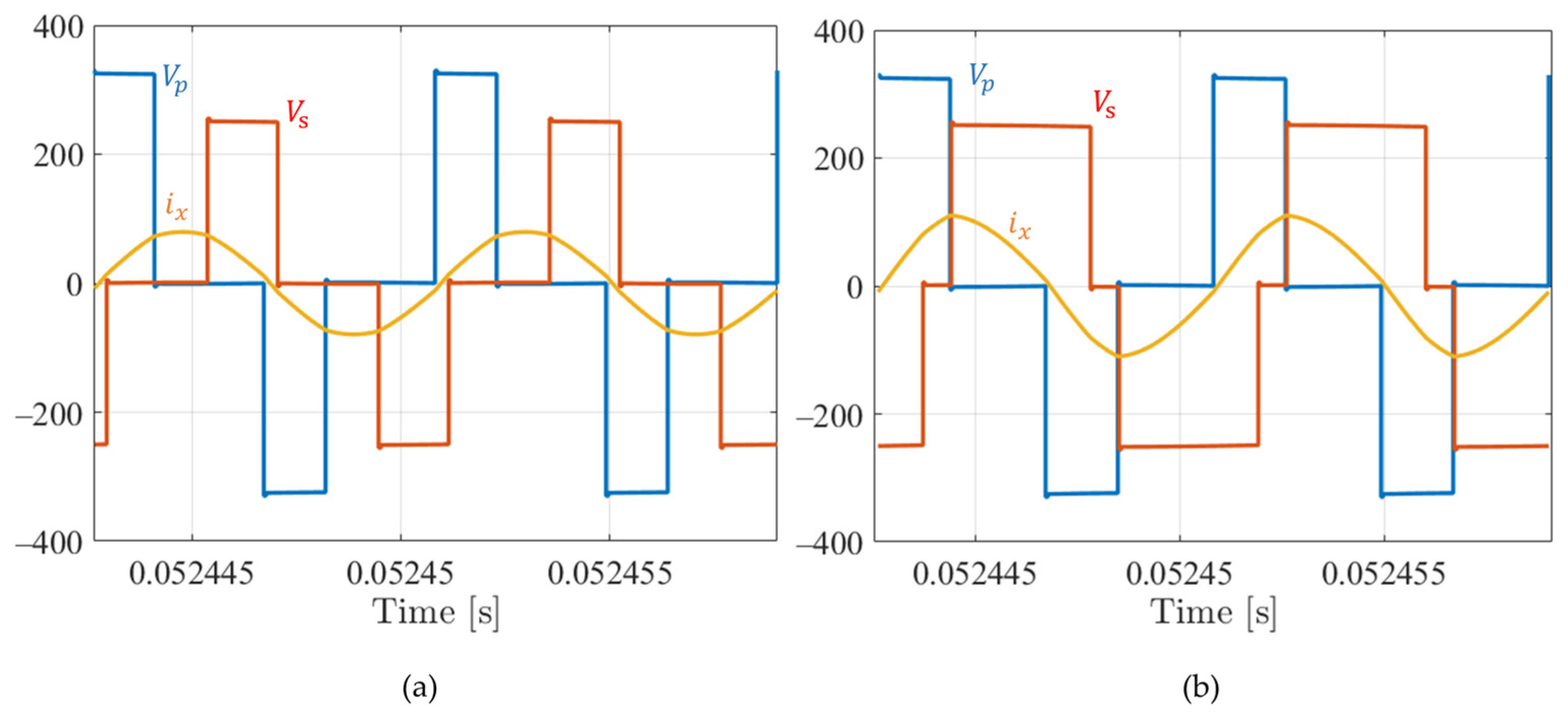
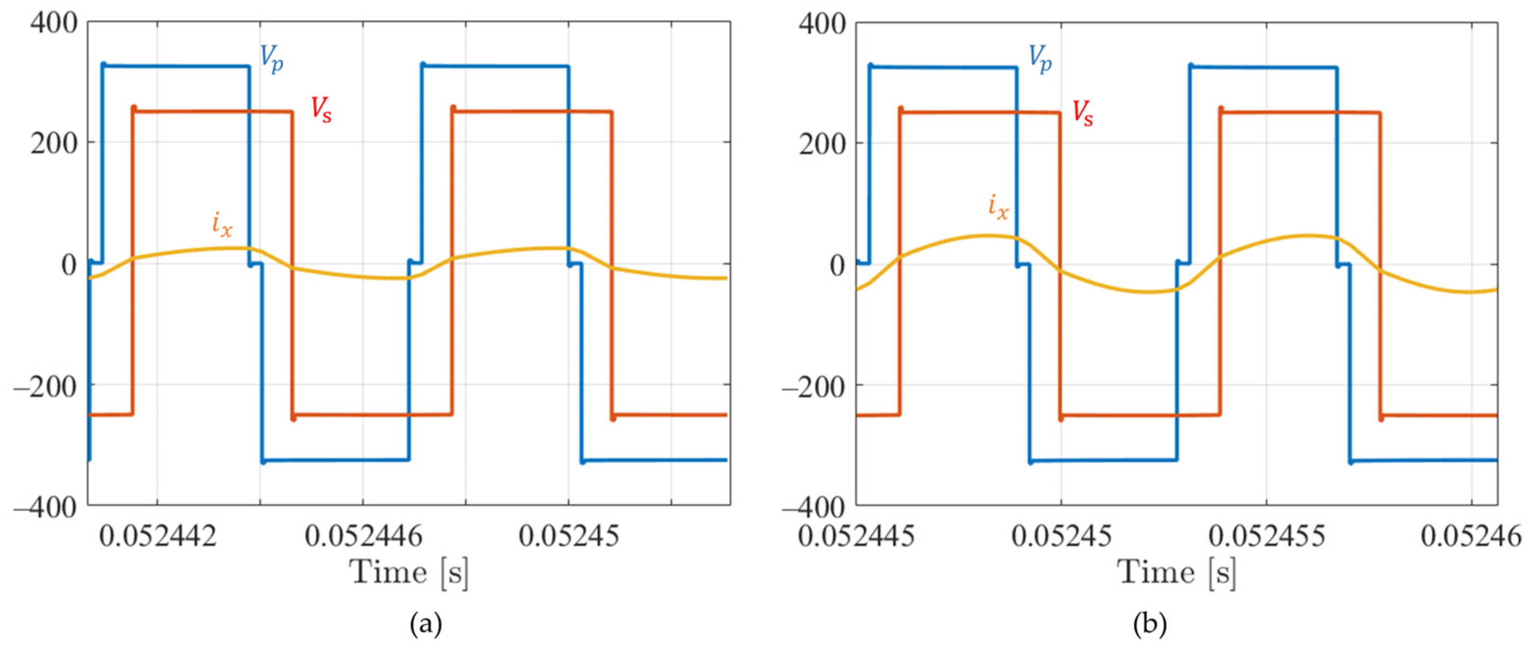
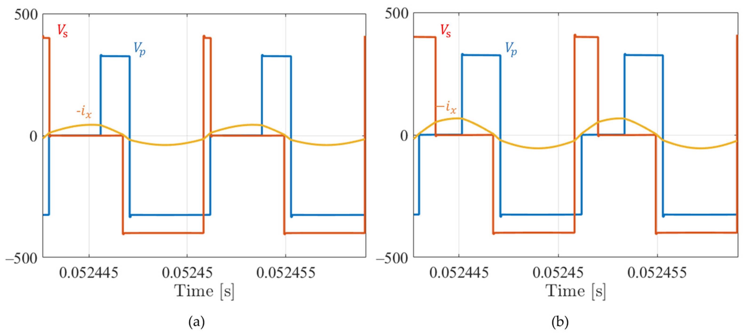
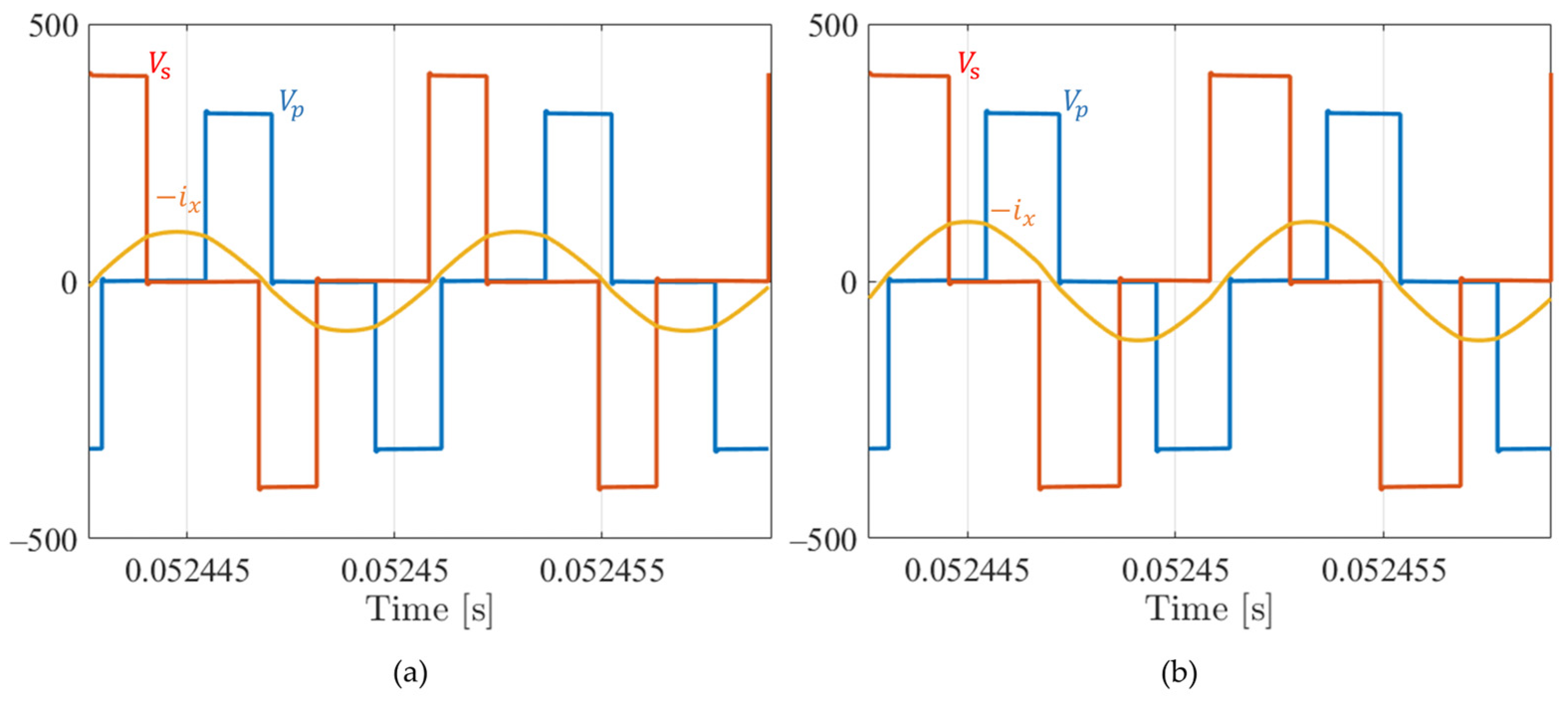
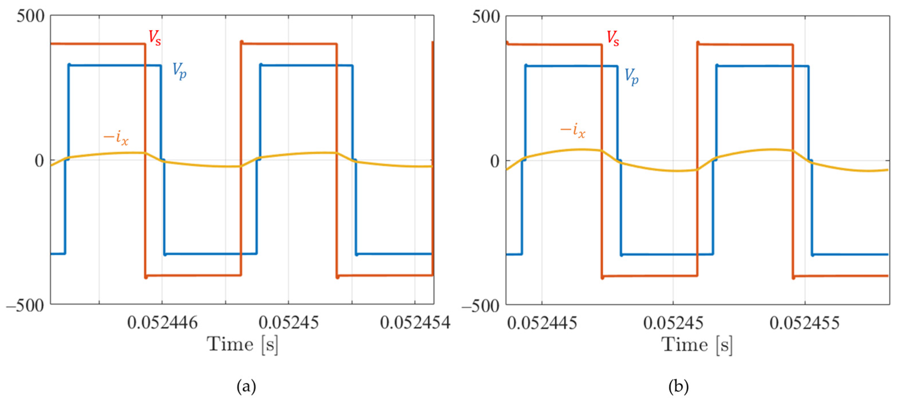
In the next figures, the resulting waveforms for forward and reverse power transfer are shown, comparing the double AVC, the TPS, and the four degrees of freedom modulation (4DOF), presented in [17]. Figure 12, Figure 13 and Figure 14 refer to the double AVC, the TPS, and the 4DOF modulation, respectively, for forward power transfer. Figure 15, Figure 16 and Figure 17 refer to the double AVC, the TPS, and the 4DOF modulation, respectively, for reverse power transfer.

5.2. HIL Simulations

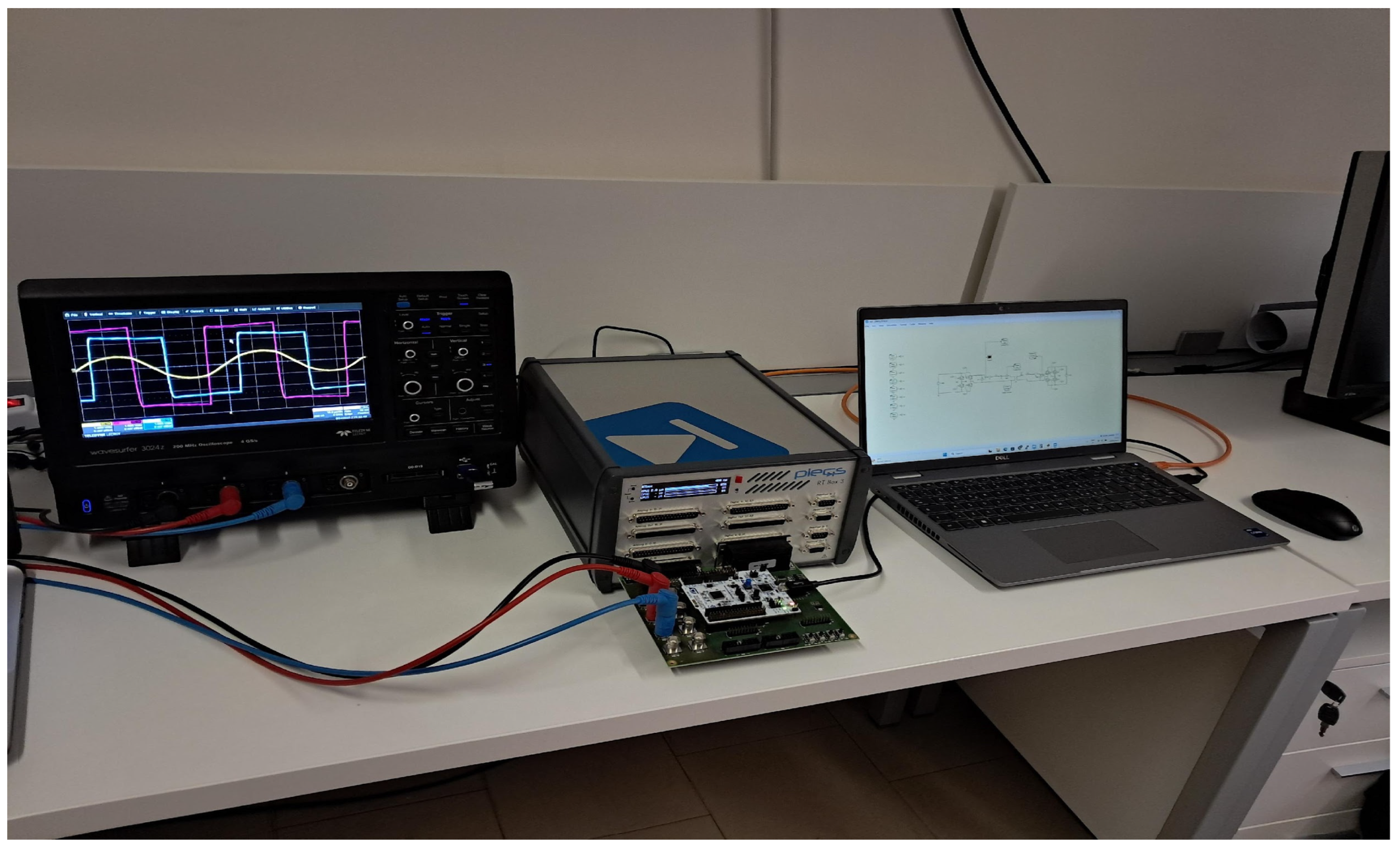
Hardware in the Loop (HIL) simulations have been carried out with the purpose of validating the control technique of the converter on an STMicroelectronics MCU (microcontroller), employing code generation. A nucleo STM32G474RE board has been programmed via PLECS 4.9.7 software while simulating the converter model on the RT Box 3. RT Box and PLECS software have been purchased from Plexim, which is also the manufacturer. The converter is simulated through the Flex Array feature; therefore, it runs on the FPGA, Xilinx Zynq Ultrascale+ ZU9EG, inside the RT Box. PWM signals are injected by four high-resolution timers (HRTIM) driven by the same master on the MCU. Due to the current limitations of the hardware, all passive components were scaled to achieve a switching frequency of 20 kHz. The control routine runs at 10 kHz in open-loop, which is fast enough to trace any variation in power output demand, under reasonable operating conditions. The setup is shown in Figure 18. The exact same control summarized in Figure 10 was implemented on the microcontroller.
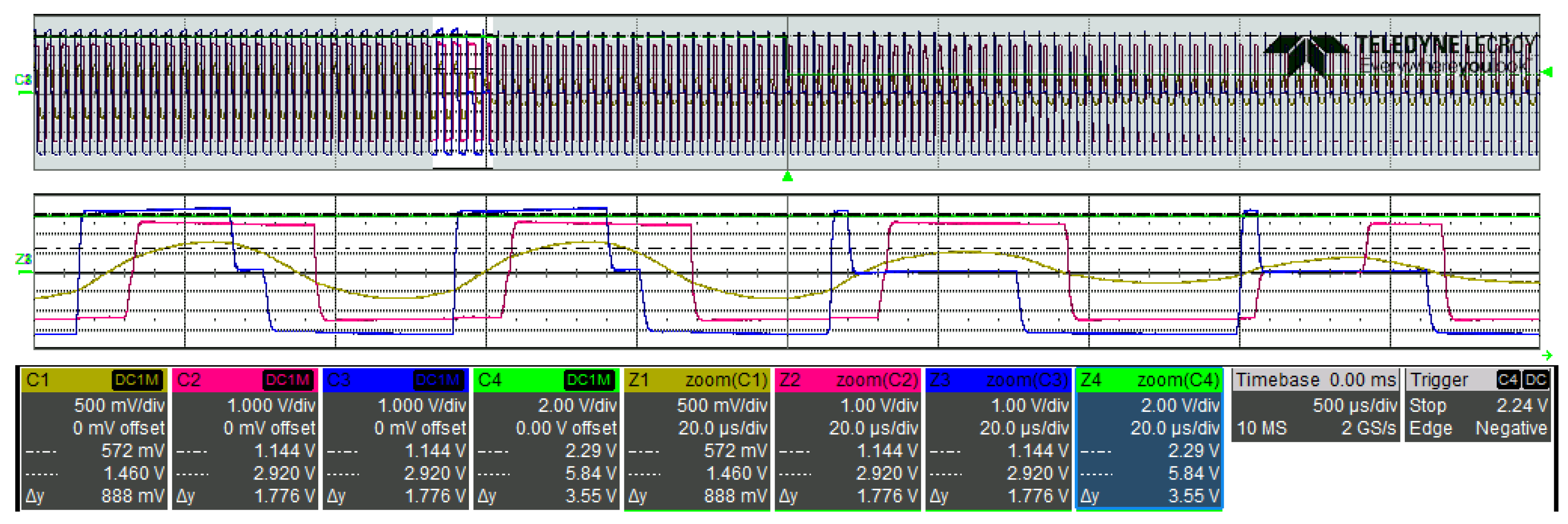
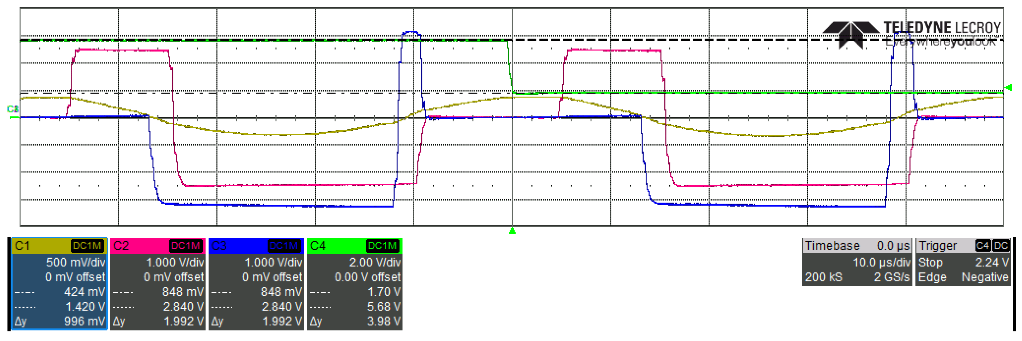
Figure 19 and Figure 20 show the behavior of the converter under a load variation, in this case during forward power transfer, but the same consideration can be made for reverse power transfer. All waveforms detected on the oscilloscope should be scaled according to the descriptions of the figures, since these signals are provided by the Analog Outputs of the RT Box and thus limited to the range [−10, +10 V]. In 500 µs, the transition is fully achieved: ZVS is not satisfied for all switches, only during this transient period.
The purpose of this subsection is limited to demonstrating the applicability on a commercial MCU and should not be intended as a substitute for the validation of the proposed modulation on real hardware. Therefore, in the following section, experimental tests have been carried out at the switching frequency of the offline simulation and on a real converter. Furthermore, different modulations have been compared therein.

6. Experimental Results

Offline simulations described in Section 5 are meant to replicate the experimental tests presented here. Of course, ringing effects and true ZVS for the switches can only be demonstrated using the real waveforms. Some operating points are shown here for the three modulation techniques: double AVC, TPS, and 4DOF [17]. In Table 6, details of the experimental setup are shown.
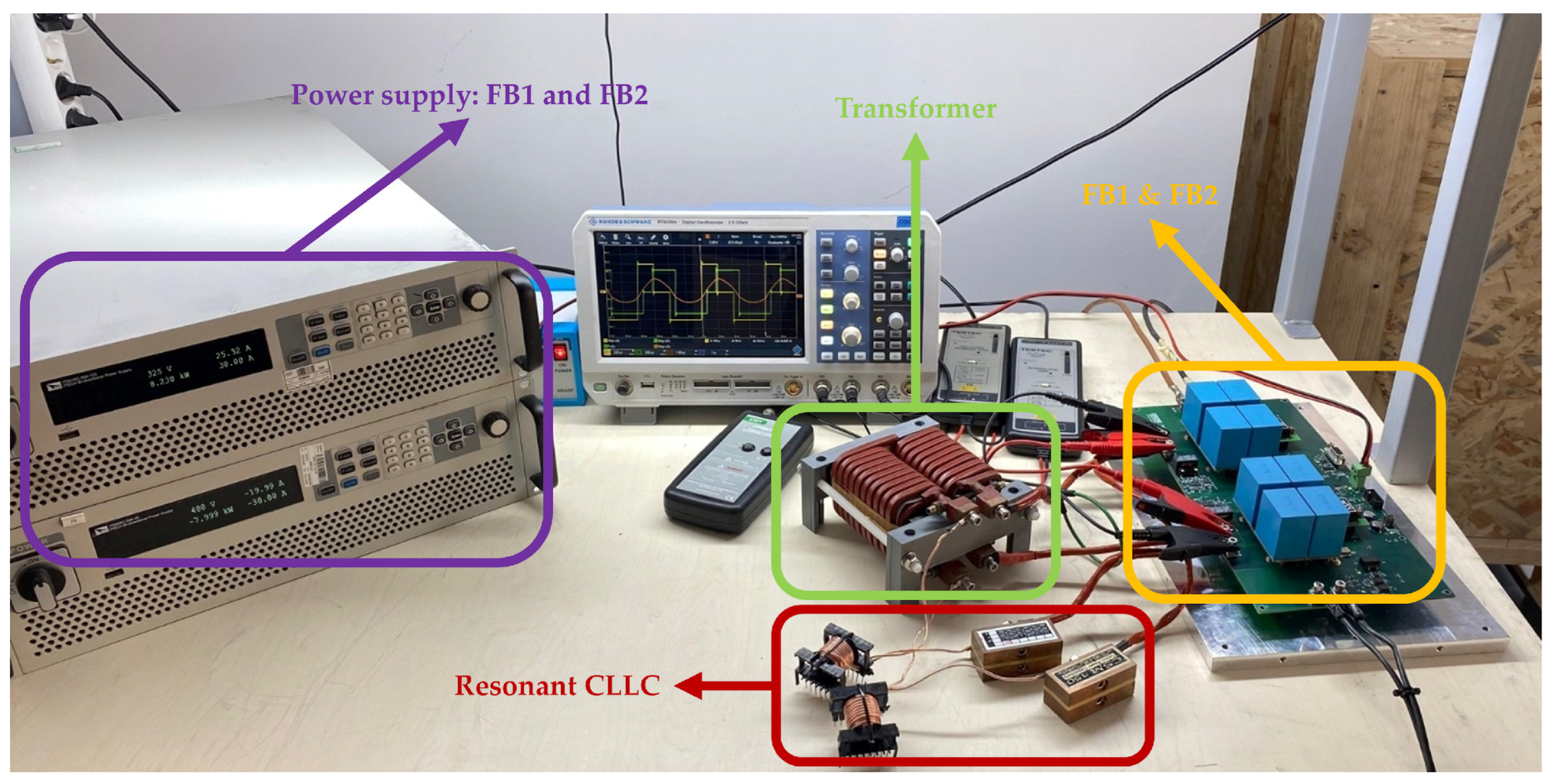
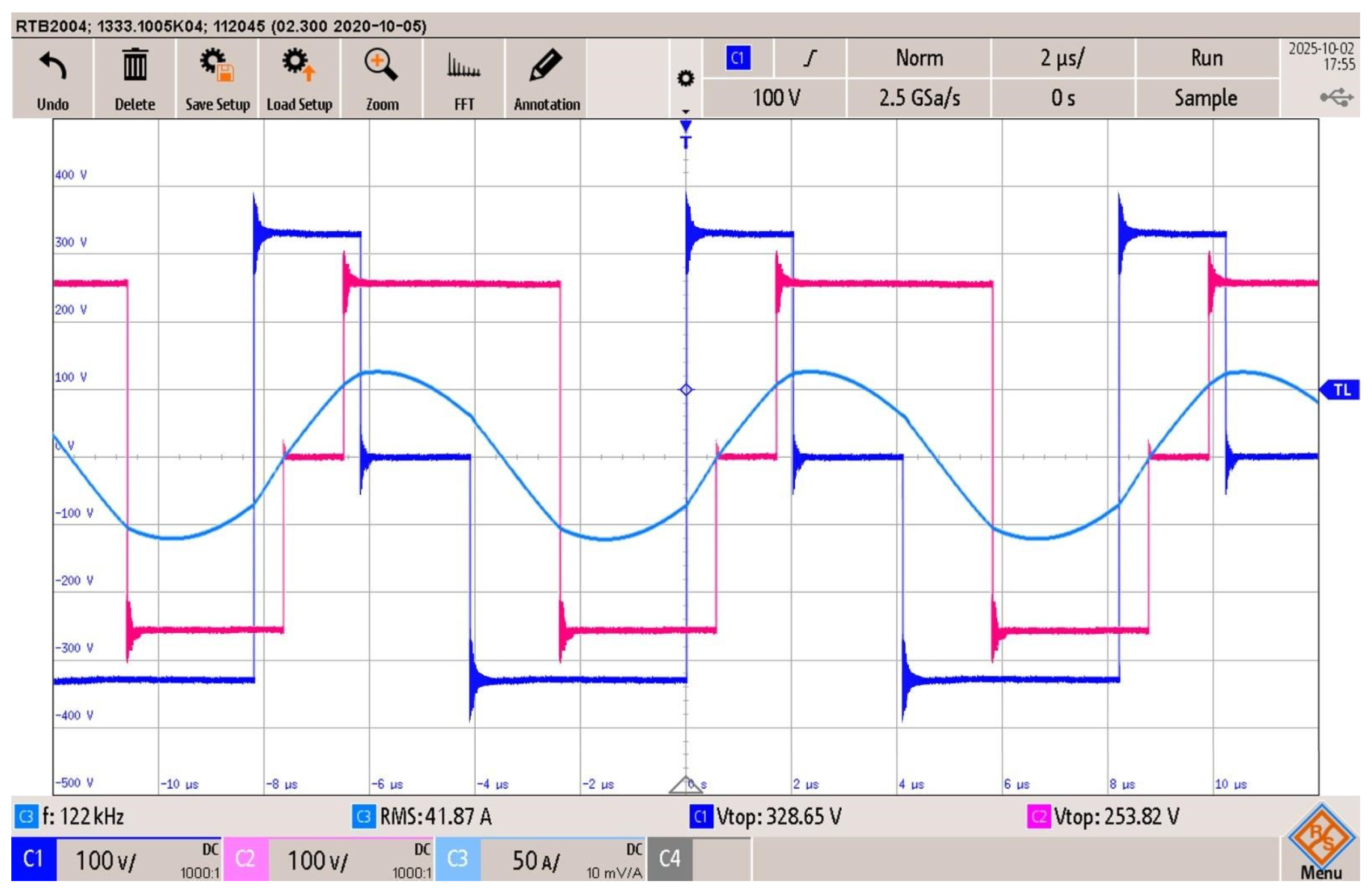
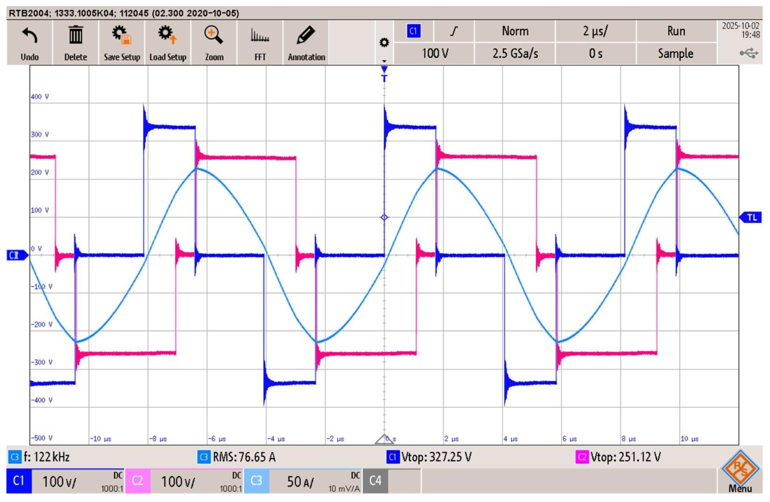
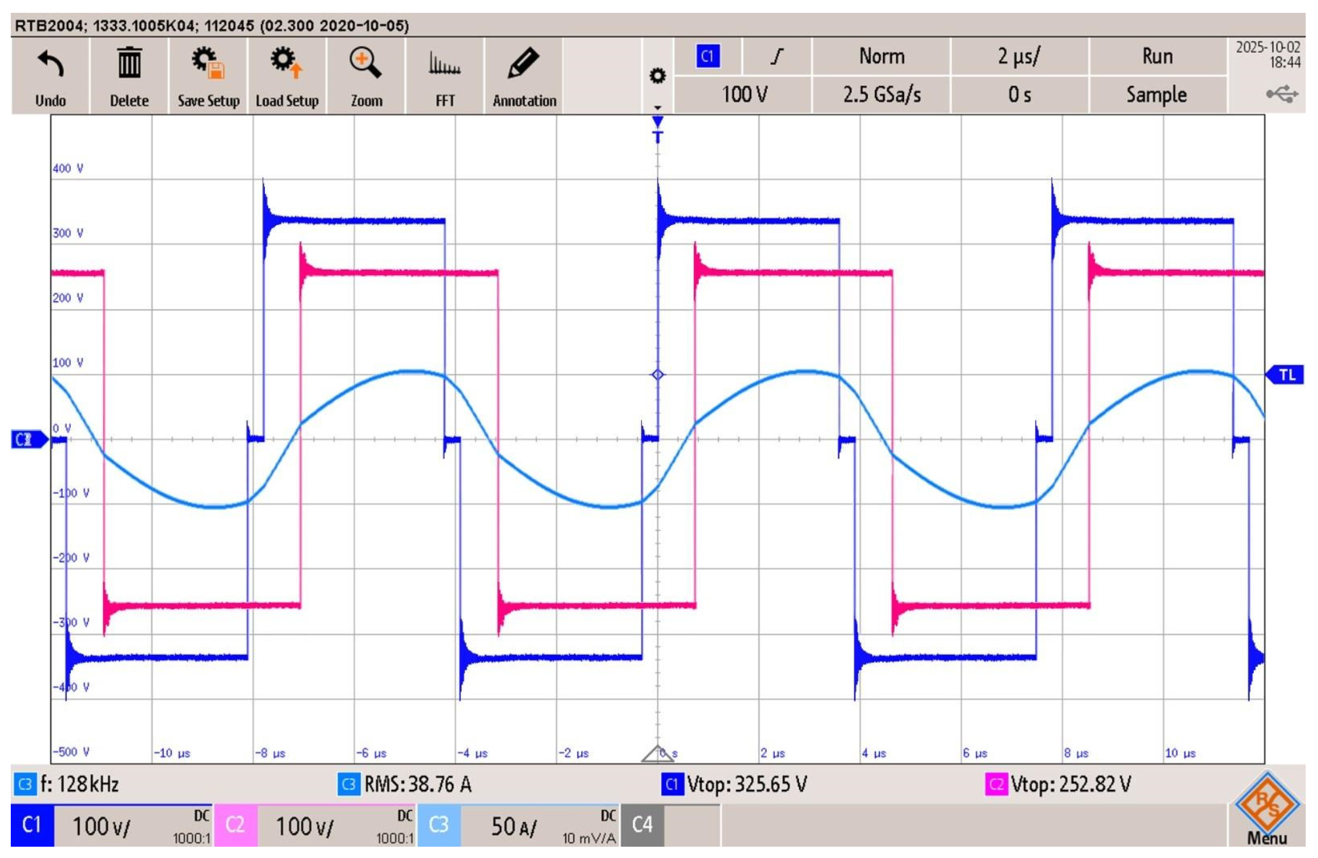
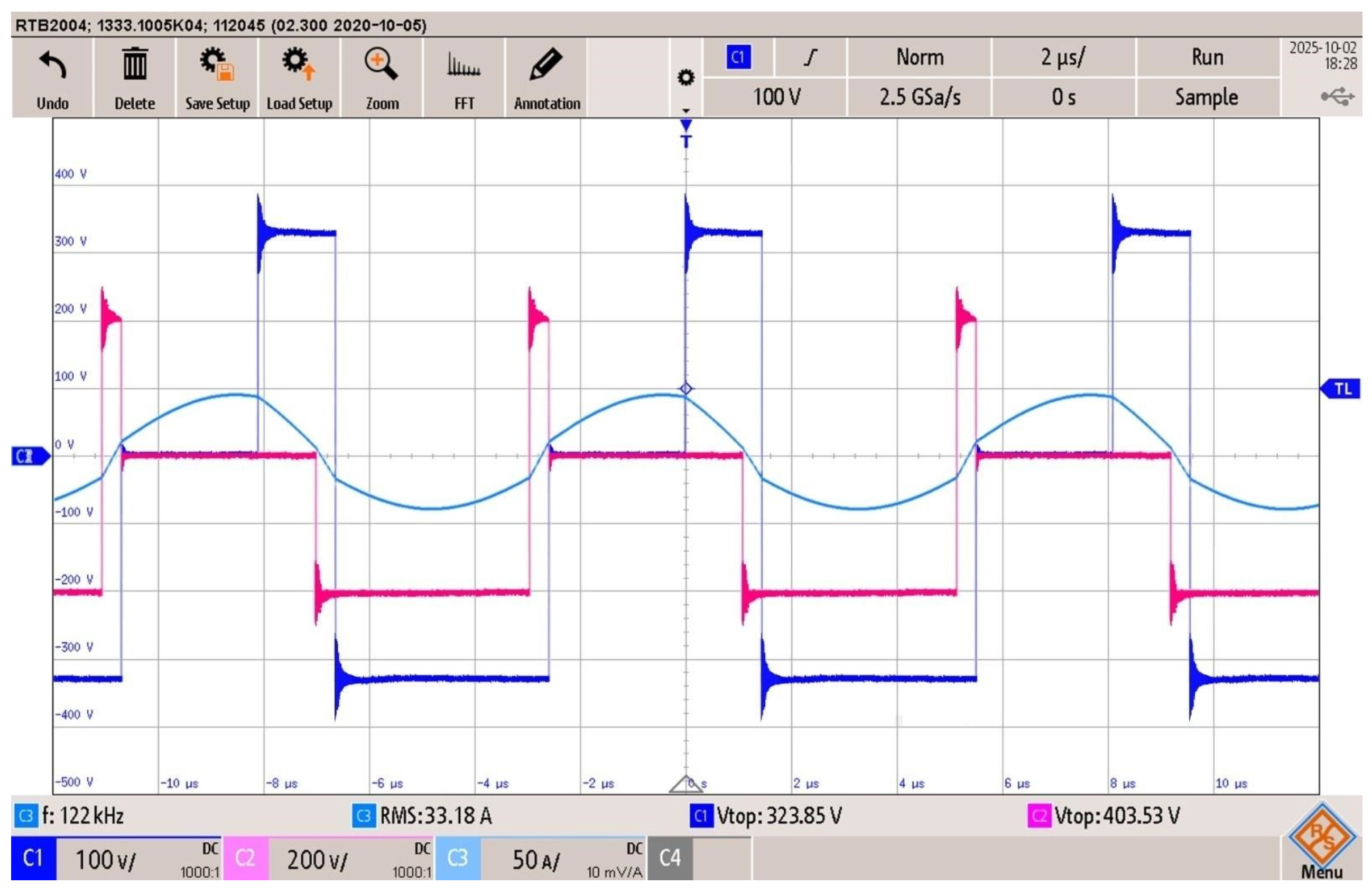
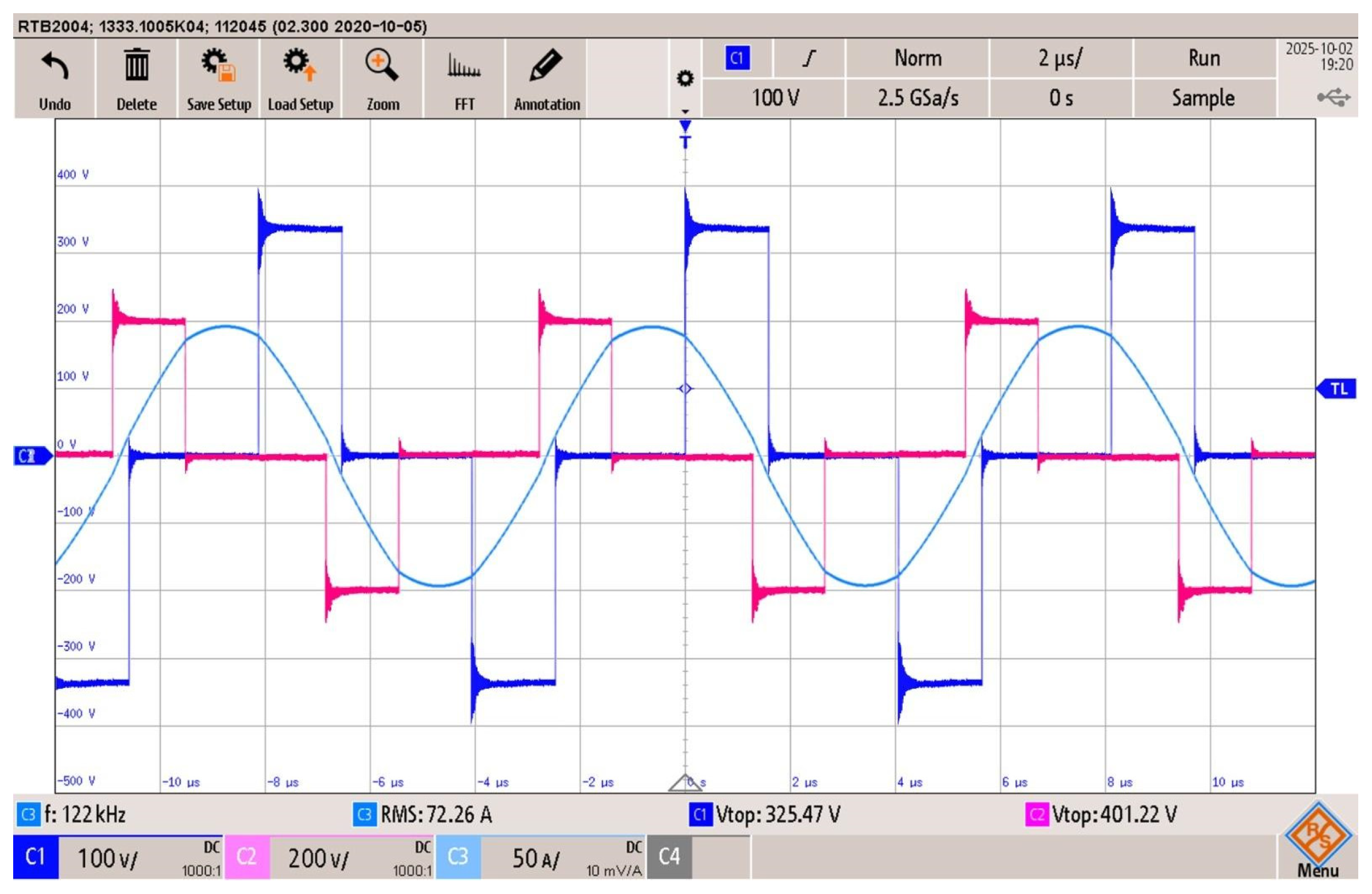
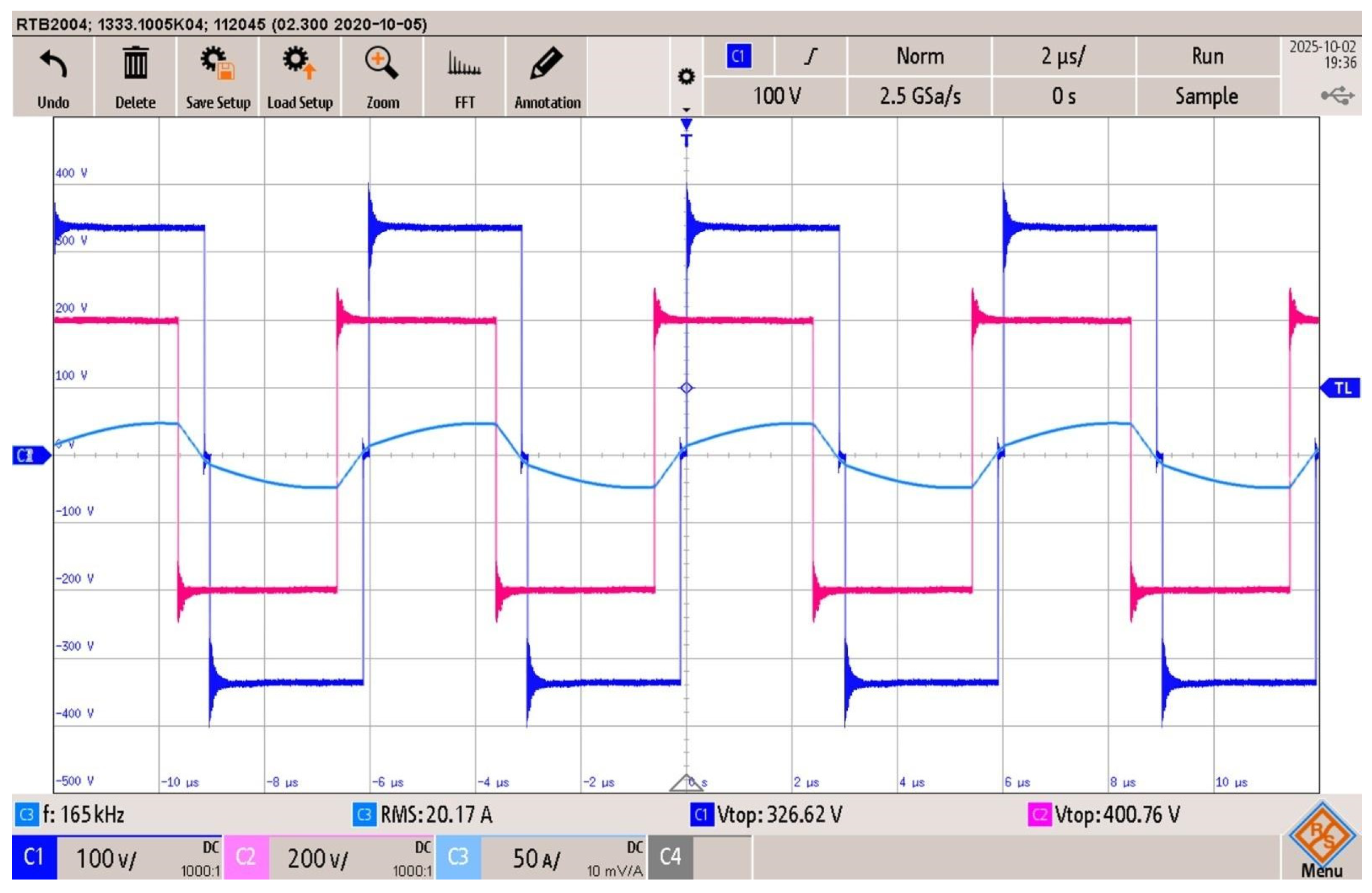
The setup of the experimental tests is shown in Figure 21, and the control board is under the converter. Control and modulation were implemented on the FPGA SoC Zynq 7000 by AMD/Xilinx using VHDL. As demonstrated in Section 5, control and modulation can also be implemented on a commercial microcontroller. In Figure 21, the experimental setup is presented: two full bridges are visible on the right along with two power supplies on the left. The transformer, additional resonant inductances, and resonant capacitors are external. The control board is instead under the converter. Experimental waveforms are summarized in Figure 22, Figure 23, Figure 24, Figure 25, Figure 26 and Figure 27. Those figures represent two operating points (one for battery charge and one for battery discharge): the maximum output power is not considered here, because every modulation technique would tend to the condition θ = π 2 ,   α p =   α s = 0 . Therefore, the difference in terms of the RMS current and efficiency would be minimal. It is clear from the tests that the double AVC modulation improves the efficiency and reduces the tank current with respect to the TPS modulation at fixed frequency. The 4DOF allows lower tank currents, even though the operating frequency has been selected manually by means of trial and error to reach ZVS and required output power. However, converter control is much easier when the double AVC modulation is implemented and for even larger power ranges, the transformer would not operate at its optimal frequency range.
The double asymmetric modulation technique was proposed and described in this paper. Since it was compared to two other existing techniques, TPS and 4DOF, the following table summarizes the differences both in qualitative and quantitative terms. The efficiency in the simulations, reported in Table 7, has been calculated as in [22] and does not account for the transformer losses: estimating the transformer losses is indeed very challenging and beyond the scope of this paper. The discrepancy between the experimental tests and simulation results can be attributed to the neglect of the aforementioned losses. However, simulations have been found in compliance with the results found during the experimental tests and the switching losses analysis suggests the quantification of MOSFETs power losses. The simulated I x , r m s is very similar to the one measured experimentally.

7. Conclusions

In this paper, an innovative asymmetric modulation technique was theorized and implemented on a CLLC resonant DAB. This fixed frequency modulation was explained mathematically, employing the FHA; then, an optimal operating points algorithm was developed and a strategic interpolation of the LUTs was proposed to control the converter. Offline simulations and HIL tests were carried out to verify what had been theorized in the first part of this paper. Finally, experimental tests were performed to verify the demanded output power and that the ZVS conditions were satisfied for each switch. Throughout the PLECS simulations and experimental validation, a comparison has been carried out with two existing modulation techniques in the literature: one at fixed frequency, TPS and one at variable frequency, 4DOF. The proposed modulation allows the efficiency to be improved with respect to the TPS, while keeping a very good controllability of the converter. Moreover, choosing a fixed frequency modulation rather than a variable one allows the transformer to be sized for a specific frequency. Furthermore, it avoids the need for expensive and complex EMI/EMC additional filters, and for the same RMS current, it allows the transistors losses to be reduced. With the 4DOF modulation, efficiencies are high, but the aforementioned drawbacks still remain. Controllability of the converter was found to be very challenging with the 4DOF modulation: the experimental points have been achieved by means of trial and error. Therefore, its applicability is very difficult. The double AVC modulation manages to maintain all the advantages of a fixed frequency modulation, while noticeably improving the efficiency with respect to the existing techniques. Further work will be carried out on the proposed modulation, especially on the number of tunable degrees of freedom. It is believed that the proposed modulation will outperform the existing variable switching frequency modulations in terms of efficiency. The merits of this paper also include a complete dissertation on the control that can be implemented on a commercial microcontroller. That is demonstrated by the code generation on an STM32G474RE: an open-loop control with selective interpolation was found to be very effective in the HIL test. The same modulation was also implemented on an SoC FPGA and was applied in comparison with the aforementioned techniques on a CLLC converter. Experimental tests showed a good compliance with the simulations, especially regarding the estimation of the RMS current flowing in the tank. Among the experimental tests performed, a maximum efficiency of around 97% was found. As already mentioned, the authors are willing to further improve the modulation technique by adding other degrees of freedom and adapting the control accordingly.

Author Contributions

Conceptualization, M.V. and J.L.B.; methodology, M.V. and L.S.; algorithm and simulation, M.V.; software and validation, J.L.B.; formal analysis, F.S.; investigation, M.V. and J.L.B.; resources, J.L.B. and F.S.; data curation, C.B. and F.S.; writing—original draft preparation, M.V.; writing—review and editing, M.V.; visualization, C.B. and V.E.; supervision, C.B. and V.E.; project administration, C.B. and V.E. All authors have read and agreed to the published version of the manuscript.

Funding

This research received no external funding.

Data Availability Statement

The data presented in this study are available on request from the corresponding author. The data are not publicly available due to privacy restrictions.

Acknowledgments

The authors would like to thank the company Smart Induction Converter Technologies S.L. and the energy department of the Polytechnic of Turin, since they provided materials and instruments to validate the work.

Conflicts of Interest

Author Juan L. Bellido was employed by the company Smart Induction Converter Technologies S.L. The remaining authors: Mattia Vogni, Fausto Stella, Leonardo Stefanini, Claudio Bianchini, and Vicente Esteve declare that the research was conducted in the absence of any commercial or financial relationships that could be construed as potential conflicts of interest. The authors declare that this study received support from Smart Induction Converter Technologies S.L. The company was not involved in the study design, collection, analysis, interpretation of data, the writing of this article, or the decision to submit it for publication.

References

  1. Wouters, H.; Martinez, W. Bidirectional Onboard Chargers for Electric Vehicles: State-of-the-Art and Future Trends. IEEE Trans. Power Elect. 2024, 39, 693–716. [Google Scholar] [CrossRef]
  2. Kasper, M.; Burkart, R.M.; Deboy, G.; Kolar, J.W. ZVS of Power MOSFETs Revisited. IEEE Trans. Power Elect. 2016, 31, 8063–8067. [Google Scholar] [CrossRef]
  3. Tang, Y.; Hu, W.; Chen, Z.; Huang, Q.; Blaabjerg, F. Dual-active-bridge DC–DC converter with auxiliary parallel networks for wide load range ZVZCS application. IET Power Elect. 2020, 13, 2569–2579. [Google Scholar] [CrossRef]
  4. Chu, C.-L.; Chen, Y. ZVS-ZCS bidirectional full-bridge DC-DC converter. In Proceedings of the 2009 International Conference on Power Electronics and Drive Systems (PEDS), Taipei, Taiwan, 2–5 November 2009; pp. 1125–1130. [Google Scholar] [CrossRef]
  5. Saeed, S.; Garcia, J.; Georgious, R. Dual-Active-Bridge Isolated DC–DC Converter With Variable Inductor for Wide Load Range Operation. IEEE Trans. Power Elect. 2021, 36, 8028–8043. [Google Scholar] [CrossRef]
  6. Yaqoob, M.; Loo, K.H.; Lai, Y.M. Extension of Soft-Switching Region of Dual-Active-Bridge Converter by a Tunable Resonant Tank. IEEE Trans. Power Elect. 2017, 32, 9093–9104. [Google Scholar] [CrossRef]
  7. Malan, W.L.; Vilathgamuwa, D.M.; Walker, G.R. Modeling and Control of a Resonant Dual Active Bridge With a Tuned CLLC Network. IEEE Trans. Power Elect. 2016, 31, 7297–7310. [Google Scholar] [CrossRef]
  8. Bellido, J.L.; Esteve, V.; Jordán, J. Efficiency Optimization in Parallel LLC Resonant Inverters with Current-Controlled Variable-Inductor and Phase Shift for Induction Heating. Electronics 2024, 13, 2593. [Google Scholar] [CrossRef]
  9. Pavlović, Z.; Oliver, J.A.; Alou, P.; Garcia, Ó.; Cobos, J.A. Bidirectional Dual Active Bridge Series Resonant Converter with pulse modulation. In Proceedings of the 2012 Twenty-Seventh Annual IEEE Applied Power Electronics Conference and Exposition (APEC 2012), Orlando, FL, USA, 5–9 February 2012; pp. 503–508. [Google Scholar] [CrossRef]
  10. Harrye, Y.A.; Ahmed, K.H.; Aboushady, A.A. Comprehensive Steady State Analysis of Bidirectional Dual Active Bridge DC/DC Converter Using Triple Phase Shift Control. In Proceedings of the 2014 IEEE 23rd International Symposium on Industrial Electronics (ISIE 2014), Istanbul, Turkey, 1–4 June 2014. [Google Scholar] [CrossRef]
  11. Shi, H.; Wen, H.; Chen, J.; Hu, Y.; Jiang, L.; Chen, G. Minimum-Reactive-Power Scheme of Dual-Active-Bridge DC–DC Converter With Three-Level Modulated Phase-Shift Control. IEEE Trans. Ind. Appl. 2017, 53, 5573–5586. [Google Scholar] [CrossRef]
  12. Hebala, O.M.; Aboushady, A.A.; Ahmed, K.H.; Abdelsalam, I. Generic Closed-Loop Controller for Power Regulation in Dual Active Bridge DC–DC Converter With Current Stress Minimization. IEEE Trans. Ind. Elect. 2019, 66, 4468–4478. [Google Scholar] [CrossRef]
  13. Chen, G.; Li, X.; Zhou, S. Unified Boundary Control With Phase Shift Compensation for Dual Bridge Series Resonant DC-DC Converter. IEEE Access 2020, 8, 131137–131149. [Google Scholar] [CrossRef]
  14. Sun, X.; Wang, Z.; Zhang, Q.; Chen, G. Variable frequency triple-phase-shift modulation strategy for minimizing RMS current in dual-active-bridge DC-DC converters. J. Power Electron. 2021, 21, 296–307. [Google Scholar] [CrossRef]
  15. Zhou, S.; Wang, J.; Tang, J. A total loss minimization modulation for series-resonant dual-active-bridge dc–dc converter with triple phase shift control. Sci. Rep. 2025, 15, 5932. [Google Scholar] [CrossRef] [PubMed]
  16. Esteve, V.; Bellido, J.L.; Jordán, J.; Dede, E.J. Improving the Efficiency of an Isolated Bidirectional Dual Active Bridge DC–DC Converter Using Variable Frequency. Electronics 2024, 13, 294. [Google Scholar] [CrossRef]
  17. Yaqoob, M.; Loo, K.H.; Lai, Y.M. A Four-Degrees-of-Freedom Modulation Strategy for Dual-Active-Bridge Series-Resonant Converter Designed for Total Loss Minimization. IEEE Trans. Power Elect. 2018, 34, 1065–1081. [Google Scholar] [CrossRef]
  18. Krismer, F.; Kolar, J.W. Efficiency-Optimized High-Current Dual Active Bridge Converter for Automotive Applications. IEEE Tran. Ind. Elect. 2012, 59, 2745–2760. [Google Scholar] [CrossRef]
  19. Burdío, J.M.; Barragán, L.A.; Monterde, F.; Navarro, D.; Acero, J. Asymmetrical voltage-cancellation control for full-bridge series resonant inverters. IEEE Trans. Power Elect. 2004, 19, 461–469. [Google Scholar] [CrossRef]
  20. Mishima, T.; Koga, Y. Variable Frequency Phase-Difference Controlled CLLC Resonant Bidirectional DC-DC Converter Featuring Wide-Range ZVS Performance and Reactive Power Reduction. In Proceedings of the 2018 IEEE Energy Conversion Congress and Exposition (ECCE 2018), Portland, OR, USA, 23–27 September 2018; pp. 6283–6290. [Google Scholar] [CrossRef]
  21. Rezayati, M.; Tahami, F.; Schanen, J.-L.; Sarrazin, B. Generalized State-Plane Analysis of Bidirectional CLLC Resonant Converter. IEEE Tran. Pow. Elect. 2022, 37, 5773–5785. [Google Scholar] [CrossRef]
  22. Bianchini, C.; Vogni, M.; Chini, A.; Franceschini, G. Switching Loss Model for SiC MOSFETs Based on Datasheet Parameters Enabling Virtual Junction Temperature Estimation. Sensors 2025, 25, 3605. [Google Scholar] [CrossRef] [PubMed]
Figure 1. Series resonant CLLC Dual-Active Bridge topology.
Electronics 14 04625 g001
Figure 2. TPS modulation applied to a resonant DAB, mode 2. Primary full-bridge FB1, output voltage (blue), secondary full-bridge FB2, output voltage (red), and resonant tank or inductor current seen by the transformer primary circuit (yellow).
Electronics 14 04625 g002
Figure 3. General conceptualization of the Double AVC modulation: FB1 output voltage (blue), FB2 output voltage (red), and tank current (yellow).
Electronics 14 04625 g003
Figure 4. Modulation mode 1: β α p < θ α s < θ < β .
Electronics 14 04625 g004
Figure 5. Modulation mode 2: β α p < θ α s < β < θ .
Electronics 14 04625 g005
Figure 6. Modulation mode 3: θ α s < β α p < θ < β .
Electronics 14 04625 g006
Figure 7. Modulation mode 4: θ α s < β α p < β < θ .
Electronics 14 04625 g007
Figure 8. Modulation mode 5: θ α s < θ < β   α p < β . Primary full-bridge, FB1, output voltage (blue), secondary full-bridge, FB2, output voltage (red) and resonant tank or inductor current seen by the transformer primary circuit (yellow).
Electronics 14 04625 g008
Figure 9. Optimal operation point algorithm.
Electronics 14 04625 g009
Figure 10. Control and interpolation strategy between optimal points.
Electronics 14 04625 g010
Figure 11. CLLC Resonant DAB schematic in PLECS.
Electronics 14 04625 g011
Figure 12. Double AVC modulation. Battery charging (250 V) from the grid: (a) at 4 kW and (b) at 8 kW. FB1 output voltage (blue), FB2 output voltage (red), and current in the resonant tank (yellow, I r m s = 26.55 Arms and I r m s = 41.2 Arms).
Electronics 14 04625 g012
Figure 13. TPS modulation. Battery charging (250 V) from the grid: (a) at 4 kW and (b) at 8 kW. FB1 output voltage (blue), FB2 output voltage (red), and current in the resonant tank (yellow, I r m s = 57.48 Arms and I r m s = 74.87 Arms).
Electronics 14 04625 g013
Figure 14. 4DOF modulation. Battery charging (250 V) from the grid: (a) at 4 kW and (b) at 8 kW. FB1 output voltage (blue), FB2 output voltage (red), and current in the resonant tank (yellow, I r m s = 18.77 Arms and I r m s = 35.11 Arms).
Electronics 14 04625 g014
Figure 15. Double AVC modulation. Battery discharging (400 V): (a) at 5.4 kW and (b) 8.5 kW. FB1 output voltage (blue), FB2 output voltage (red), and current in the resonant tank (yellow, I r m s = 31.18 Arms and I r m s = 45.00 Arms).
Electronics 14 04625 g015
Figure 16. TPS modulation. Battery discharging (400 V): (a) at 5.4 kW and (b) 8.5 kW. FB1 output voltage (blue), FB2 output voltage (red), and current in the resonant tank (yellow, I r m s = 70 Arms and I r m s = 87.46 Arms).
Electronics 14 04625 g016
Figure 17. 4DOF modulation. Battery discharging (400 V): (a) at 5.4 kW and (b) 8.5 kW. FB1 output voltage (blue), FB2 output voltage (red), and current in the resonant tank (yellow, I r m s = 18.22 Arms and I r m s = 28.33 Arms).
Electronics 14 04625 g017
Figure 18. HIL simulation of the Resonant DAB CLLC converter.
Electronics 14 04625 g018
Figure 19. Battery charge: transition from 12 kW to 4 kW power (modulation transition). FB1 output voltage (blue), FB2 output voltage (pink), current in the resonant tank (yellow), and output power (green). Scales are 1:100 for the output voltages and current and 1:2000 for the average output power.
Electronics 14 04625 g019
Figure 20. Battery charge: transition from 12 kW to 4 kW power (output power transition). FB1 output voltage (blue), FB2 output voltage (pink), current in the resonant tank (yellow), and output power (green). Scales are 1:100 for the output voltages and current and 1:2000 for the average output power.
Electronics 14 04625 g020
Figure 21. Experimental setup: full-bridges, resonant capacitors, transformer, additional resonant inductors, and two bidirectional power supplies. Control board is under the converter.
Electronics 14 04625 g021
Figure 22. Double AVC modulation, battery charge at 8 kW: FB1 output voltage (blue trace), FB2 output voltage (pink trace), and resonant tank current (light blue), η =   96.3 % .
Electronics 14 04625 g022
Figure 23. TPS modulation, battery charge at 8 kW: FB1 output voltage (blue trace), FB2 output voltage (pink trace), and resonant tank current (light blue), η =   91.5 % .
Electronics 14 04625 g023
Figure 24. 4DOF modulation, battery charge at 8 kW: FB1 output voltage (blue trace), FB2 output voltage (pink trace), and resonant tank current (light blue), η =   97.2 % .
Electronics 14 04625 g024
Figure 25. Double AVC modulation, battery discharge at 5.5 kW: FB1 output voltage (blue trace), FB2 output voltage (pink trace), and resonant tank current (light blue), η =   96.8 % .
Electronics 14 04625 g025
Figure 26. TPS modulation, battery discharge at 5.5 kW: FB1 output voltage (blue trace), FB2 output voltage (pink trace), and resonant tank current (light blue), η =   87.7 % .
Electronics 14 04625 g026
Figure 27. 4DOF modulation, battery discharge at 5.5 kW: FB1 output voltage (blue trace), FB2 output voltage (pink trace), and resonant tank current (light blue), η =   97.4 % .
Electronics 14 04625 g027
Table 1. TPS modulation modes.
Mode t 0 t 1 t 2 t 3 t 4
10 d 3 · T s w 2 d 2 + d 3 · T s w 2 d 1 · T s w 2 T s w 2
20 d 1 · T s w 2 ( d 2 + d 3 1 ) · T s w 2 d 3 · T s w 2 T s w 2
30 d 1 · T s w 2 d 3 · T s w 2 d 2 + d 3 · T s w 2 T s w 2
40 ( d 2 + d 3 1 ) · T s w 2 d 1 · T s w 2 d 3 · T s w 2 T s w 2
50 ( d 3 + 1 ) · T s w 2 d 1 · T s w 2 ( d 2 + d 3 ) · T s w 2 T s w 2
60 ( d 2 + d 3 1 ) · T s w 2 d 3 · T s w 2 d 1 · T s w 2 T s w 2
Table 2. Double AVC modulation modes.
Mode t 0 t 1 t 2 t 3 t 4 t 5
10 β α p ω θ α s ω θ ω β ω θ + β α s ω
20 β α p ω θ α s ω β ω θ ω θ + β α s ω
30 θ α s ω β α p ω θ ω β ω θ + β α s ω
40 θ α s ω β α p ω β ω θ ω θ + β α s ω
50 θ α s ω θ ω β α p ω β ω θ + β α s ω
Table 3. Possible sequences of AVC modulation.
Sequence S 1 S 2 S 3 S 4 Q 1 Q 2 Q 3 Q 4
110010110
210011010
310010101
410011001
510100110
601010110
710101010
810100101
901011010
1001010101
1110101001
1201011001
1301100110
1401101010
1501100101
1601101001
Table 4. Association between modes and sequences.
ModeSeq. 1Seq. 2Seq. 3Seq. 4Seq. 5Seq. 6
1157111613
2157141613
3127111613
4127141613
5124111613
Table 5. CLLC Resonant DAB converter parameters.
ParameterSymbolValue
Rectified primary voltage V p 230 2 V
Battery voltage range V s 250 ÷ 400 V
Output power range P o 4 ÷ 14 kW
Transformer ratio n 1
Magnetizing inductance L m 5.266 mH
Resonant inductance L f 1 8.1   µH
Resonant capacitor C f 1 330 nF
Resonant frequency f r ~ 97.35 kHz
Fixed switching frequency f s w 122 kHz
Table 6. Main parameters of the experimental tests.
ParameterSymbolPart NumberValue
Rectified primary voltage V p / 230 2 V
Battery voltage range V s / 250 , 400 V
Output power range P o / 4 ÷ 14 kW
Transformer ratio n /1
Magnetizing inductance L m / 5.266 mH
Leakage inductance L l k / 3.85 µH
Resonant additional inductance L f 1 / 4.25 µH
Resonant capacitor C f 1 CSM 150 330 nF
Resonant frequency f r / ~ 97.35 kHz
2 parallel SiC MOSFETs/C3M0040120K/
SoC FPGA/Zynq 7000/
Fixed switching frequency (AVC and TPS) f s w / 122 kHz
Variable switching frequency (4DOF) f s w / 113.5 165 kHz
Table 7. Comparison of the three modulation techniques.
Modulation Technique FeatureTPS4DOFDouble AVC
SymmetryYesYesNo
Switching frequency [kHz]122 (fixed)113.5–165 (variable)122 (fixed)
ControlEasyHardEasy
EMI/EMCLowHighLow
Sim. I x , r m s [Arms]74.87 (+8 kW)35.11 (+8 kW)41.2 (+8 kW)
70.0 (−5.5 kW)18.22 (−5.5 kW)31.8 (−5.5 kW)
Sim. η [%]92.65 (+8 kW)97.4 (+8 kW)97.1 (+8 kW)
89.65 (−5.5 kW)96.8 (−5.5 kW)96.6 (−5.5 kW)
Exp. I x , r m s 76.65 (+8 kW)38.76 (+8 kW)41.87 (+8 kW)
72.26 (−5.5 kW)20.17 (−5.5 kW)33.18 (−5.5 kW)
Exp. η [%]91.5 (+8 kW)97.2 (+8 kW)96.3 (+8 kW)
87.7 (−5.5 kW)97.4 (−5.5 kW)96.8 (−5.5 kW)
Disclaimer/Publisher’s Note: The statements, opinions and data contained in all publications are solely those of the individual author(s) and contributor(s) and not of MDPI and/or the editor(s). MDPI and/or the editor(s) disclaim responsibility for any injury to people or property resulting from any ideas, methods, instructions or products referred to in the content.