1. Introduction
Electronic sensors play a significant role and compete with traditional methods in detecting substances in various fields such as industry, biotechnology, medicine, and environmental protection, thanks to their sensitivity, compactness, cost-effectiveness, ease of maintenance, and compatibility with modern information technologies and electronics. The most common types of electronic chemical sensors are conductometric, potentiometric, and amperometric sensors. In modern physics and analytical chemistry, determining of the quantitative content of a chemical element in a substance mixture is an important task.
Sensors are considered indispensable instruments for performing quantitative and qualitative analyses. The advancement of modern sensor technologies is largely determined by the pursuit of novel efficient elements with enhanced selectivity, integration potential, and sensitivity [
1,
2,
3,
4,
5]. The responses of each low-selectivity element may generally vary slightly depending on the adsorbing substance type, but the combination of responses from such elements creates a unique fingerprint of the substance. Thus, a highly sensitive system can be created using a sensor matrix with low selectivity.
The complementing of information from other sensors and the enhancement of sensitivity and selectivity is enabled by an individual sensor through the implementation of an innovative physical approach for the conversion of external influence into an informative signal [
6].
An electronic tongue can be defined as a powerful analytical tool constructed from an array of elements that exhibit cross-sensitive responses to analyte solutions. It utilizes a suitable pattern recognition method to achieve the required overall selectivity [
7,
8]. The properties of the tongue elements can be further modified by incorporating coatings containing oxides and chalcogenides, lipid membranes, organic polymers, and noble metals. In recent times, thanks to biosensing technologies, systems have been developed for the detection of viruses and screening of specific low-molecular-weight compounds in biological samples. In light of these circumstances, research on recombination structures through the photoelectric conversion mechanism is important. The selection of this sensor is motivated by its combination of properties that provide certain advantages over other well-known sensor transducers.
Comparatively, straightforward technical implementation is enabled by these structures, while a transduction principle distinct from the well-studied light-addressable potentiometric sensor (LAPS) is employed [
2].
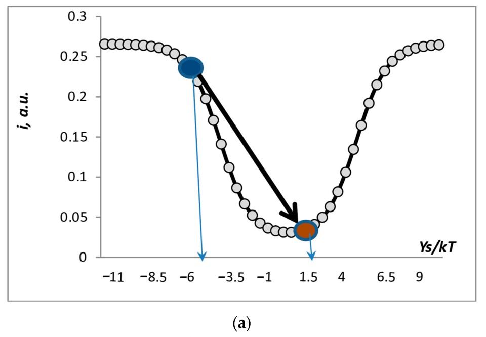
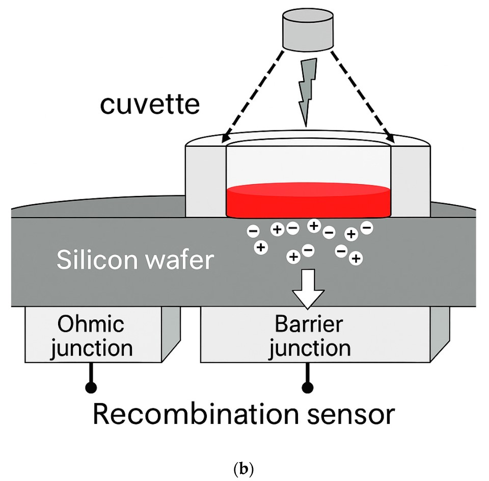
The strong reactivity toward analytes, comprising molecules with innate or induced dipolar properties, and the comparatively straightforward instrumental application are combined in sensors of this type. The parameter directly measured is the photocurrent in a silicon wafer with a deep junction barrier, exposed to light in the active absorption region. Sensors based on charge recombination mechanisms were developed based on the effect of controlled and consistent modifications related to recombination dynamics of the semiconductor surface interface caused by adsorption [
9].
The physicochemical conditions at the interface define the photoelectric current, which functions as the informative signal and distinguishes this sensor. Effective application requires the sensor’s photocurrent to be strongly influenced by variations in the surface carrier recombination rate. This requirement is fulfilled when the light absorption and charge separation areas are distinctly localized.
The processes involving contact with the analyte, which determine the response, occur in a very thin monomolecular layer, resulting in high sensitivity. In accordance with its operating principle, the sensor enables the controlled allocation of characteristics (functionalization) across the surface and also allows light-addressing during testing, enabling its operation in accordance with the electronic nose paradigm. Structurally, the recombination sensor comprises an illumination unit that delivers sequential irradiation to specific surface points of the semiconductor barrier structure, as well as units that measure the corresponding photocurrents, amplify them, and visualize the results by generating LBIC maps, which illustrate the distribution of photocurrent under surface contact with different analytes [
1]. Direct registration of enzymes or other biological molecules using such structures is hindered due to the absence of molecular fragments with pronounced dipole moments in the structure. However, intermediate products can exhibit activity in terms of influencing the parameters of recombination centers at the interface
SiOx/
Si. Several important aspects should be noted. It is now beyond doubt that changes in the expression of specific enzymes, such as lactate dehydrogenase (LDH), as well as an increase in total LDH activity in biological samples (organism fluids), serve as important diagnostic indicators for numerous diseases, including solid tumors, autoimmune diseases, cardiovascular and cerebrovascular diseases, acute conditions, and blood disorders. Existing methods for determining LDH activity typically require expensive equipment or exhibit low sensitivity and selectivity. However, we have found that our method can effectively record LDH activity in human serum samples. Laboratory-based biochemical approaches to pathological diagnosis typically focus on determining biomarkers, such as alanine aminotransferase (ALT) and aspartate aminotransferase (AST). Elevated levels of these biomarkers in the blood often correlate with liver tissue damage. Given the significance of determining ALT/AST activity in human blood for screening metabolic processes and cardiovascular health, the development of efficient methods for rapidly determining enzyme activity is of great practical importance. While chromatographic and fluorescent methods have been introduced into clinical practice, their use is limited due to the requirement for expensive equipment and susceptibility to factors such as illumination, pH, and temperature. Additionally, electrochemical sensors have shown instability and short operating times. However, the successful application of a recombination sensor for real-time detection of ALT/AST activities in the blood plasma of rats has been demonstrated. Therefore, our concept of using a recombination sensor for real-time determination of ALT/AST enzymatic activities offer promising prospects for the development of screening platforms. This semiconductor sensor structure can offer increased reliability and technical simplicity compared to existing prototypes of electrochemical sensors.
In stationary versions, the illumination unit is based on a helium–neon laser with a positioning system that uses acousto-optic crystals. Since intense focused laser illumination can damage proteins, enzymes, and other sensitive molecules, the use of an LED matrix reduces the peak optical intensity, minimizing photodegradation and preserving the enzymatic activity and stability of plasma components. The ability to control the illumination intensity is essential for enhancing the informativeness of measurements, as the brightness directly affects the balance between carrier generation and recombination. This capability enables the investigation of different photoconductivity regimes and the evaluation of recombination parameters. Varying the illumination makes it possible to detect nonlinear effects, optimize measurement conditions for a given sample, and obtain a more comprehensive picture of the spatial inhomogeneity of photoactivity. While adjusting the intensity of a helium–neon laser is technically challenging and requires additional optical components, the use of an LED matrix allows simple software-controlled brightness modulation, making such systems more flexible and efficient for practical LBIC investigations. In this study, an efficient and compact version of the illumination unit based on semiconductor LEDs is proposed for the recombination sensor structure that meets the requirements of compactness and rapid analysis of analytes. This compact approach opens broad possibilities for the development of sensor structures adapted for biomedical applications. Portable versions can be easily integrated into various automated monitoring systems for the assessment of human health or environmental conditions.
3. Results and Discussion: Implementation of an LED-Based Illumination Unit
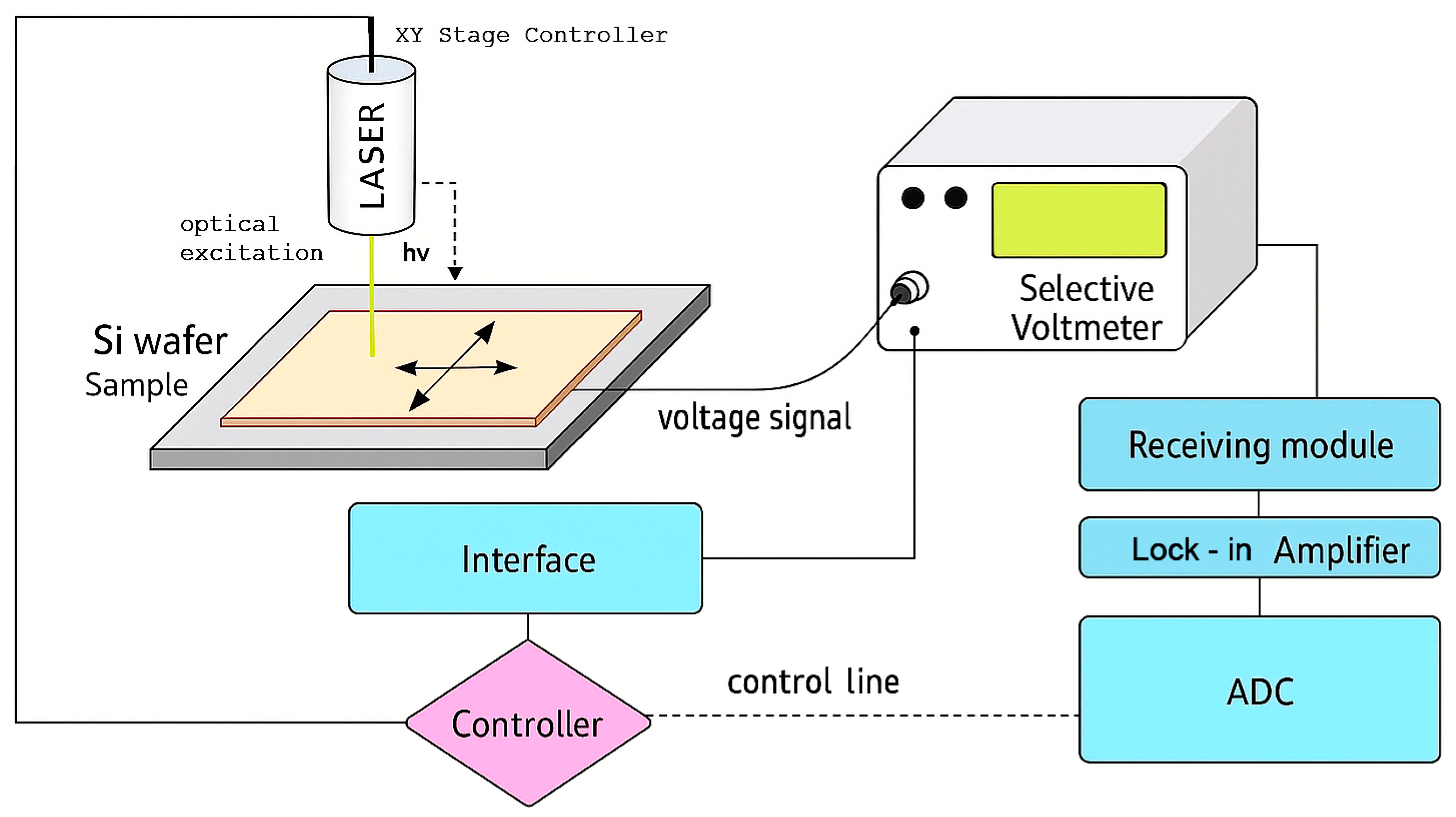
The photorecombination sensor collects information regarding the amplitude of the photocurrent, which varies depending on the coordinates at different scanned points of the semicoductor sample with the analyte. The selective voltmeter Selective Voltmeter is implemented to measure electrical signals generated by the sensor and is tuned to the modulation frequency of the LED-based illumination unit. The receiving module Receiving Module receives signals from the selective voltmeter and transmits them to the instrumental amplifier to ensure proper sensitivity and measurement accuracy. The ADC (analog-to-digital converter) converts analog signals obtained from the amplifier into a digital format that can be processed by a computer or microcontroller. The controller oversees the operation of the entire system, including processing acquired data, controlling the operation modes of other units, and synchronizing data transmission to external devices or systems via the interface. The interface can be implemented in the form of a UART or Wi-Fi module to offer convenient data storage or interaction with the user.
As can be seen, the LED-based illumination unit is extremely important in portable implementations of recombination-based sensors, as it determines the parameters of through-current photocurrent. Firstly, this unit should provide a maximum set of functions similar to more complex schemes with laser surface scanning (such as the ability to change intensity, modulation parameter frequencies, and exposure time of specific points). Secondly, the set of emitters in the LED-based illumination unit should be sufficient to obtain high-quality photocurrent mapping with adequate resolution (relative to a certain class of analytes). And finally, such a unit should have compact dimensions and an acceptable cost. It is clear that the specific task and type of analysis will determine the technical implementation of the unit. The proposed model implementation of the illumination unit allows the studying and testing of the sensor’s operation in basic operating modes.
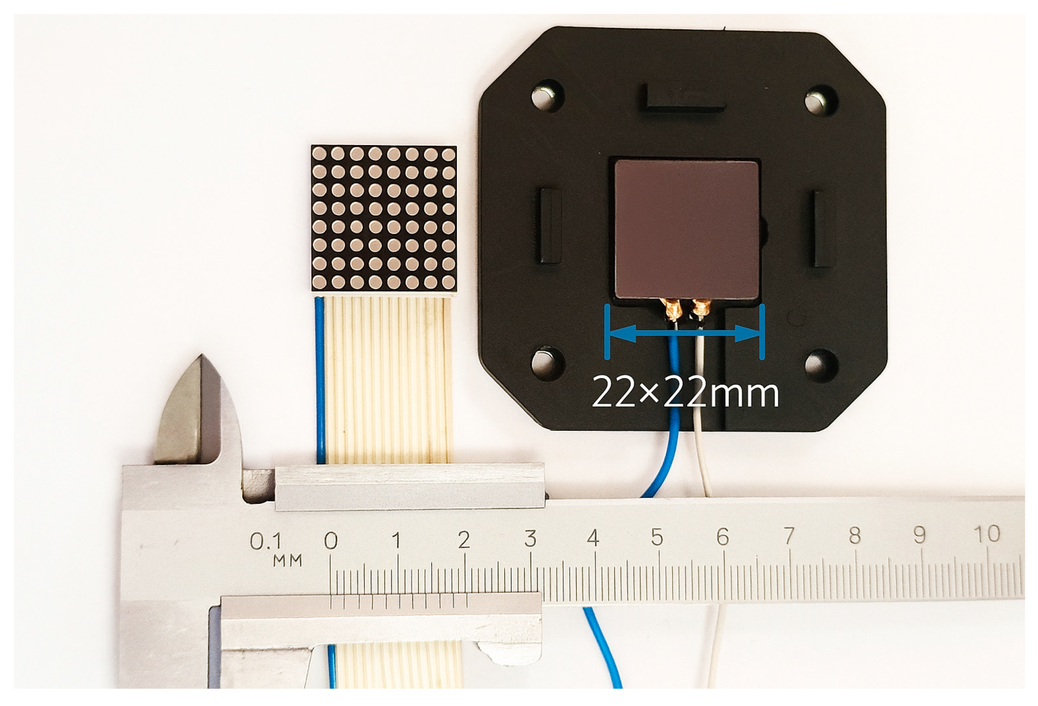
Let us consider some design features of the portable unit. The
Figure 3 presents a photo of the LED-based Illumination unitillumination unit, sensor, and cuvettes, allowing us to understand the main design features and characteristic dimensions.
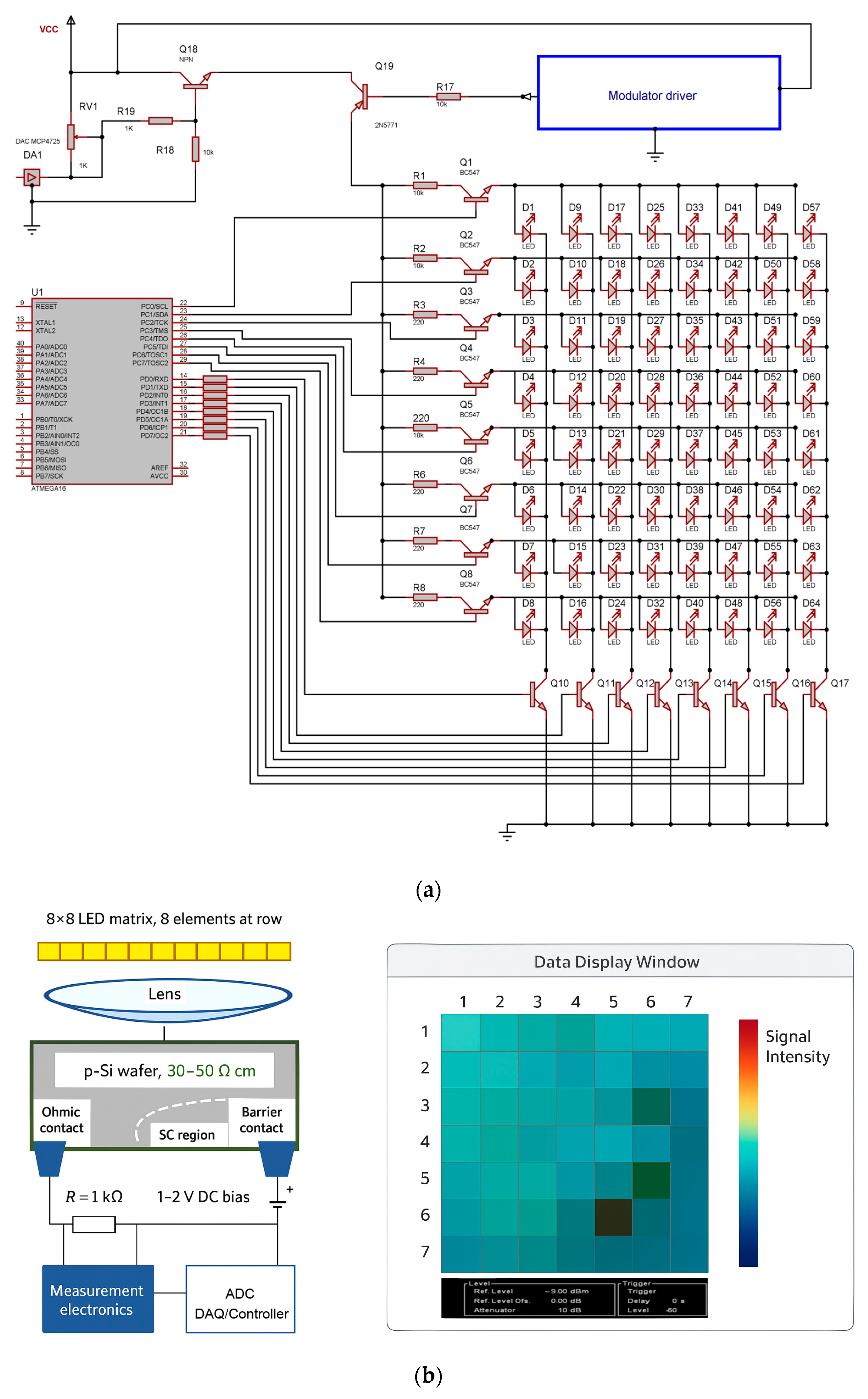
The schematic and simplified electrical schemes of the unit are shown in
Figure 4a,b. The number of LEDs should be compatible with the cuvette dimensions, and thus, no principal restrictions exist. In our case, eight LEDs per line is quite acceptable. The size and the type of the LED-based is mainly determined by the size of the photorecombination sensor. The microcontroller drives the LED anode rows. The base terminals of transistors are driven via resistors by the microcontroller outputs, thereby controlling the LED Q10–Q17 transistors connected with the cathodes of the LED matrix. The tenth output of the microcontroller is connected to the input signal (CLK) of the modulation module, serving as the synchronization input. To limit the current to the collectors of BC547 Q1–Q9 transistors, resistors of 220 Ω (R1–R8) are employed. Brightness can be adjusted programmatically or via potentiometer R5, with the collectors of these transistors connected to the output of the digital-to-analog converter through transistor Q18, allowing the control of brightness over a wide range. The Q1–Q8 transistors are driven through the port outputs, as shown in
Figure 4a. The parameters of the 1088BS LEDs employed in the LED-based illumination unit were as follows:
The peak emission wavelength (λ_peak) ranged from 630 to 640 nm. The forward current and voltage were IF = 10–20 mA and VF = 1.8–2.4 V, respectively. The pulse-width modulation (PWM) frequency was 1 kHz, with a duty cycle adjustable from 10% to 100% depending on the desired brightness level. The illuminance at the sample plane (2.2 × 2.2 mm) was approximately IV ≈ 13.5–39.5 cd at IF = 10 mA, with field uniformity maintained within ±5% across the same area. The working distance was set to 5 mm. The thermal stabilization time required to reach steady-state brightness was approximately 30 s. The optical path exhibited a spectral bandwidth of 620–650 nm with a central wavelength of 635 nm. The analog-to-digital converter (ADC) provided a resolution of 12 bits over an input voltage range of 0–3.3 V.
Figure 5 represents principal scheme of transformations of the photorecombination signal in the sensor. Before using such systems, calibration is performed to ensure the correspondence of the obtained results to real values. Standard samples or known reference values of photocurrent can be used for this purpose. Validation of the obtained results was carried out to confirm the accuracy and reliability of the system. This was performeddone by comparing it with a classical LBIC scanning system using control samples. This allowed us to qualitatively evaluate how well the results of portable versions correspond to the requirements of sensitivity and detection resolution. In principle, different analytes (like water, isopropyl or alcohol) can be used to investigate and clarify the operation of recombination sensor. In such cases, it is possible to achieve significant relative changes in the photocurrent and ensure their high reproducibility.
Distilled water is a “model” analyte with pronounced dipole structure, so its use to the investigation and analyze the operation of a compact sensor system with an LED illumination unit.
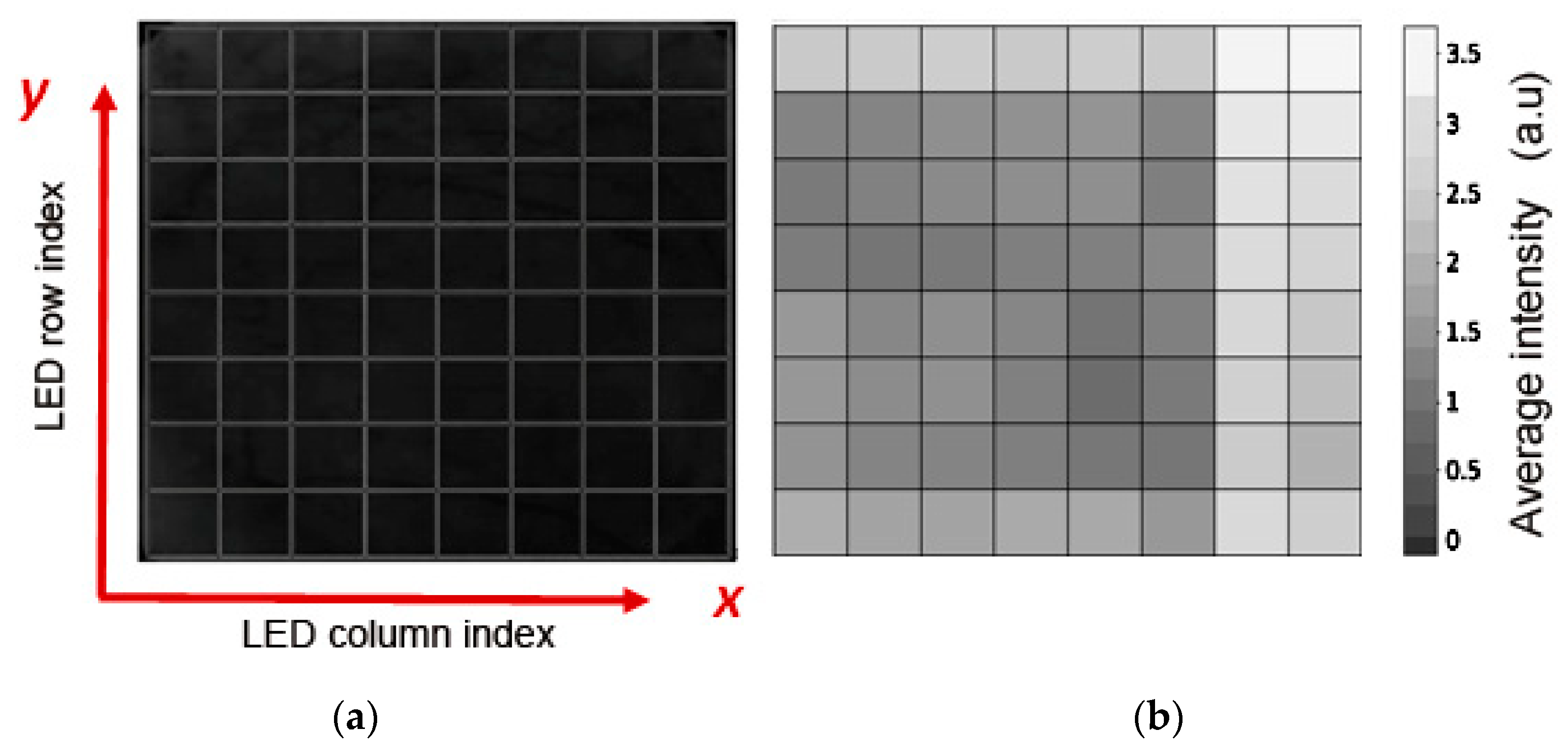
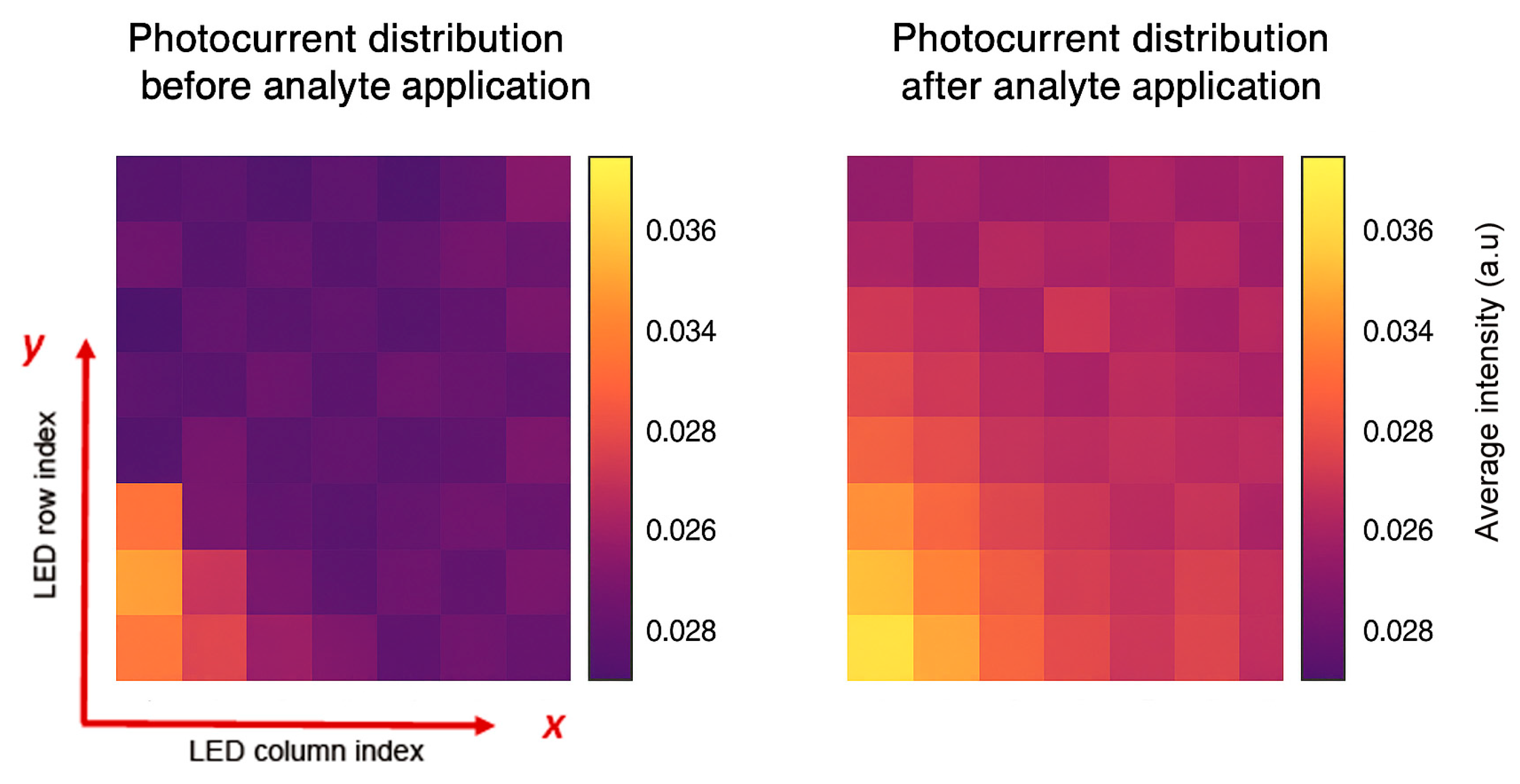
Figure 5a shows typical maps of photocurrent distribution (
i1) under the conditions of surface contact with air, whereas
Figure 5b shows typical maps of photocurrent distribution (
i2) under the conditions of surface contact with distilled water. Both cases using the developed illumination unit. The measurements of photocurrent were performed using selective voltmeter, as presented in
Figure 2. Brighter regions
Figure 5a,b correspond to higher photocurrents at the respective surface points (
x,
y). It is easy to see that this ratio varies at different points. This fact can be explained by the non-uniform distribution of the initial on the surface [
1].
The processes of signal conversion during photocurrent measurements are illustrated in detail in
Figure 5. Suppose one of the 64 LEDs in the LED-based illumination unit illuminates the sensor surface at the point (
x,
y). A photocurrent is generated in the measurement circuit, which is significantly influenced by the surface recombination rate S. This variable voltage, after passing through a 1 kΩ resistor, is fed into the analog input of the UNIPAN 233 selective nanovoltmeter (Unitra-Unipan, Warsaw, Poland) which is designed for the selective measurement of extremely small AC signals spanning frequencies from 1.5 Hz to 150 kHz. The available measurement ranges include 10 nV, 100 nV, 300 nV, 1 µV, 3 µV, 10 µV, 30 µV, 100 µV, 300 µV, 1 mV, 3 mV, 10 mV, 30 mV, and 100 mV, with selectivity per octave at 0, 18, 36, or 54 dB
Figure 4b. The amplitude of the voltage from the analog output (proportional to the amplitude of the photocurrent) is then fed into a 16-bit ADC for conversion to digital code, followed by storage and processing. The UNIPAN 233 must be tuned to the LED modulation frequency. Gradually, all 64 LEDs conduct a scanning of the sensor surface. If necessary, the full cycle can be repeated to generate a dataset for averaging measurement. As a result, we obtain an 8 × 8 matrix of photocurrent amplitudes, which can be conveniently presented as maps (arbitrary units), as shown in
Figure 4. It is worth noting that when using distilled water, our illumination unit enabled a threefold increase in signal strength on average within the 1 mV range of the UNIPAN 233. This is illustrated in
Figure 4 and
Figure 5. Therefore, we have every reason to affirm the reliability of detection using the LED-based illumination unit. In the case of using an LED laser, the signal may be higher on average, and the resolution would naturally be greater; however, for the development of portable versions, the influence of these factors can be moderately simplified.
In our system, several different scanning algorithms can be applied for measuring photocurrent in sensors. One such algorithm is step-by-step scanning, which involves sequentially scanning through the rows or columns of the sensor matrix. This approach reduces scanning time since each point is scanned only once. However, this method may not account for localized temporal variations. Another approach is zonal scanning, where the sensor surface is divided into several areas, and each area is fully scanned before moving on to the next. This allows for a focus on specific areas, increasing measurement accuracy in critical zones, but it may miss changes in other zones. Selective scanning involves measuring only at a few points, which may be random or chosen based on certain criteria. This ensures quick results with fewer measurements, but it may reduce accuracy and increase the risk of missing important anomalies. Adaptive scanning adjusts the strategy based on intermediate results, allowing for increased scanning frequency in areas with anomalies, thereby improving accuracy in critical zones while reducing scanning time in less important areas.
When the experiment is intended to obtain the most accurate and reliable data for each individual sensor point, the n-fold measurement algorithm with result-averaging is employed. It reduces the impact of random fluctuations and noise, thereby enhancing measurement accuracy, improving signal stability assessment at specific points, and detecting potential local anomalies. Depending on the number of repetitions, this method can be more efficient than performing multiple scans of all points. Additionally, conducting all measurements for a single point within a short time frame helps minimize the influence of external factors such as temperature changes or drift. The choice of method depends on the specific task and the requirements for accuracy and detail. If it is important to gain a general understanding of the photocurrent distribution across the entire sensor surface, performing multiple scans of the entire surface is advisable.
To confirm the high resolution of our photocurrent measurement system, a series of experiments was and the results were analyzed using various averaging methods. It was found that the data could vary with different types of averaging, indicating the need for precise control and validation of the system.
In instances where the measurement results did not exhibit consistent datasets, samples were subjected to further analysis using liquid chromatography coupled with mass-selective detection (Agilent 1100 Series Liquid Chromatograph, Agilent Technologies, Santa Clara, CA, USA). This additional analysis was performed to accurately delineate the composition and characteristics of the substances under investigation.
The assessment of measurement accuracy and uncertainty was performed using statistical methods, including averaging the results for each sensor point and analyzing data variability. The results indicated that the maximum measurement uncertainty is ±50 nA, confirming the high accuracy and reliability of the system. The possible errors Δ
i1/
i1 and Δ
i2/
i2 are determined by the standard setup for photocurrent measurement, which results in an error of several percent. In the case of expressing the result as the ratio of photocurrents
i1/
i2, the relative error is obviously doubled
ε = Δ
i1/
i1 + Δ
i2/
i2 [
8]. At the same time, the contact of the surface with the analyte induces a two- to threefold increase in photocurrent across the surface. Therefore, we can conclude that our LED system provides an intensity that is sufficiently adequate for detection.
This approach, in principle, can enhance the adaptability of the structure for various practical applications. It should be noted that the proposed unit facilitates the regulation of illumination intensity and modulation frequency of individual LEDs within LED-based, as well as the implementation of diverse polling algorithms on the sensor surface. The suitability of the illumination unit and the surface point-polling algorithm for the development of mini-systems based on the recombination conversion principle is illustrated by this test example. In this instance, the number of probed surface points corresponds to the number of light sources in the array (64 LEDs). These illustrations demonstrate the operation of the recombination sensor structure with the developed unit and a standard photodetector.
To average the photocurrent values and obtain more accurate distributions that characterize the analyte, our system has the capability to average the results in each of the 64 illuminated points.
The system software performs a statistical analysis of the acquired data, taking into account accuracy indicators such as root mean square error, correlation, and confidence intervals. Theoretical calculations of photocurrent may also be carried out to assess the representativeness of the photocurrent measurements for a specific analyte, considering the physical and chemical properties of the analyte and its possible interactions with the sensor surface. Physically, the detection mechanism relies on changes at the surface band-bending resulting from the contact between the silicon surface and the polar molecules of the analyte, as well as their influence on the recombination parameters at the interface. Additionally, the quality of illumination and scanning modes of the sensor surface enable photocurrent measurements with sufficient accuracy to differentiate the tested analytes [
8].
The fundamental characteristic of this approach, utilizing the portable illumination unit, is the novel physical mechanism of transformation and the relative simplicity of technical implementation. Therefore, the proposed transducer holds promise as a foundation for the development of a new non-destructive method that is technically straightforward. The deep barrier sensory structure has demonstrated sufficient sensitivity to discern the local electric field associated with different molecular structures.
The detection of ALT and transaminase activities in rat blood plasma with a recombination sensor is shown in
Figure 6. The sensor operates based on enzyme-mediated chemical reactions specific to ALT.
No catalytic effect was observed in the absence of the ALT enzyme. This result was obtained in an experiment performed without blood plasma, under conditions where the enzymatic reaction could not occur. The observed changes in the photocurrent can be explained by the recharging of recombination centers and the corresponding variation in the recombination rate. The change in the effective negative charge of the reagents, including the substrates and reaction products, can be predicted from their dissociation constants for α-ketoglutarate and aspartate with α-ketoglutarate.
Thus, the detection of ALT is fundamentally possible due to specific chemical reactions catalyzed by the corresponding enzyme, although the effect is indirect. Six series of experiments were conducted, confirming this result and demonstrating good reproducibility. By comparing the laser-based and LED-based LBIC systems, the following parameters can be distinguished: the photocurrent amplitude is 35–45 nA for the He-Ne laser system and 10–20 nA for the LED-based unit; the signal-to-noise ratio (SNR) is 18 dB and 25 dB, respectively; the spatial resolution is 50 μm and 0.6–2.7 mm; the detection limit (ΔI/I) is approximately 5% and 7%; and the cost of the illumination unit is high for the laser system and low for the LED-based system.
These biomarkers have recently been utilized for prognostic assessment in severe pathologies, including COVID-19 and metastatic malignancies [
20,
21,
22,
23,
24].
In addition, mechanisms for compensating temperature variations and monitoring environmental conditions can be employed to ensure the reliability and stability of the system. This may involve cooling or heating systems, temperature and humidity sensors, as well as algorithms for automatically adjusting system parameters based on changes in environmental conditions. These methods and mechanisms are aimed at achieving accuracy, reliability, and stability in the recombination sensor system. They enable reliable and precise measurements of photocurrent, ensuring the representativeness of the obtained data and determination of the physical characteristics of the analyte.
The experimental results described in our works [
15,
19] were conducted under laboratory conditions. To enhance the functionality of the technology in this regard, it is essential to develop a portable version of the devices that would be distinguished by compactness, autonomy, and the ability to be operated remotely. For practical applicability, the specified technique (technology) must be able to be operated in real-timeanalyze samples of biological materials obtained from patients. Therefore, the design of the portable, compact 8 × 8 illumination LED unit presented here represents an important step towards the practical realization of our previous results. In contrast to multiplexing methods implemented with application-specific integrated circuits (ASICs), the proposed system utilizes an LED matrix controlled by a microcontroller. This architecture enables fully programmable illumination patterns and facilitates synchronization with the photorecombination sensor. It allows rapid adjustment of illumination parameters through firmware updates without hardware modifications. Consequently, the system is readily scalable, cost-effective, and better suited to various modes of biological fluid analysis compared with ASIC-based multiplexed solutions [
25,
26].
The Internet of Things (IoT) is concept that involves embedding physical objects with sensors, processing ability, software, and the technologies that enable connection and data exchange between devices and systems over the internet. The IoT comprises electronics, communication, and computer science. It has many applications, including fields as trade, living spaces, health care, transportation, and many others. Since it invades many areas, the studies in this field attract many researchers. The successful implementation of the IoT requires solving several problems:
1. Security: Because data transferred via networks may be subjected to cyberattacks, which can destroy the operation of infrastructure [
27,
28], so the studies in this attract attention of many researchers [
29]
2. Privacy: IoT devices and systems are often left vulnerable to intrusions. As a result, user privacy is compromised. This can lead to fraud and the misuse of collected data [
30,
31]
3. Interoperability and Standardization: Lack of unified standards is a frequent problem because different manufacturers use specific tools, instruments, equipment, and proprietary communication protocols, hindering device compatibility. This can lead to problems with integration between devices, networks, and platforms [
32,
33]. This can be dangerous, even at the level of units used. For instance, in this case, mismatch between imperial and SI units led to the crash of a costly Mars probe [
34].
4. Data Acquisition, Processing, Management acquisition, processing, management and Storage: Numerous devices generate huge amounts of data, creating challenges in acquisition, storage, transmission, and analysis [
35,
36,
37].
5. Energy and Resource Efficiency Limited battery life: Many IoT sensors and sensor nodes work autonomously, relying on low-power batteries, which limit their term operation. In addition, the production and disposal of billions of devices and cells contribute to electronic waste [
38,
39].
6. Scalability and Network Congestion: As the number of connected devices grows, networks can lose their ability to transfer data and some problems with network traffic can occur, such as latency and unreliable data transfer. In many cases the quality of traffic is crucial (e.g., in health care, autonomous vehicles, and many other fields) because they require stable, reliable, and low-latency communication [
40,
41].
7. Legal, Ethical, and Governance Challenges: The IoT is a rapidly developing area, involving technology and regulations. There may be unclear responsibilities for data ownership and data misuse. In addition, ethical issues also arise, because constant monitoring and predictive analytics can lead to loss of privacy and algorithmic bias [
42].
8. Maintenance and Lifecycle Management: Many IoT devices require regular updates of software to avoid security risks. Devices and systems also need require management to supervise, repair, and timely replace worn, outdated, or obsolete devices [
43,
44,
45,
46].
9. Sensors, Instrumentation, and Metrology: We believe that the whole idea of IoT is heavily reliant on accurate data. Measurement data must be accurate, timely, and reliable. This is often underestimated. There are numerous studies focused on improving the accuracy of sensors, the least accurate node of the measurement chain [
8,
47,
48]. Successful solutions to this problem can considerably improve industrial performance in many areas [
46,
49,
50,
51,
52,
53].
In this paper, we present a novel solution that balances measurement accuracy (we focus on problem 9 from the list above) and cost efficiency as we use relatively cheap and easily accessible components and improve their accuracy. The proposed method demonstrates adequate accuracy for its intended applications and offers flexibility, which are both needed for ad hoc measurements. Integration of a microcontroller enables network connectivity, allowing the device to operate as part of an IoT system, providing instant access to measurement results and allowing data processing.
The integration of an IoT component into the portable system based on photorecombination sensors enhances its functionality and operational flexibility. Wireless data transmission enables the transfer of signals and measurement parameters to cloud databases in real time, allowing remote monitoring of the stability of photorecombination characteristics. To ensure compatibility with the IoT concept, the developed system incorporates an ESP32 wireless module connected via a UART interface to the main ATmega16 controller. The ATmega16 microcontroller is responsible for controlling the LED matrix and synchronizing the measurement process, whereas the ESP32 module handles data packet generation and wireless transmission. The data, including induced current values, measurement point coordinates, and timestamps, are transmitted in JSON format via the MQTT protocol over a Wi-Fi network compliant with the IEEE 802.11 b/g/n standard. The typical data transfer rate reaches up to 1 Mbit/s, and the delay between signal acquisition and its appearance in the remote storage or user interface does not exceed 50 ms.
To enhance system reliability, data are buffered in the internal flash memory of the ESP32 in the event of a connection loss. This architecture adheres to the edge-IoT concept, where partial signal processing is performed directly on the device, reducing network load and enabling near-real-time visualization of the LBIC signal distribution through a remote web interface. A compact microcontroller-based LED illumination unit for recombination-based sensor structures is presented. The illumination system employs an 8 × 8 LED matrix, enabling programmable spatial excitation patterns over a 2.2 × 2.2 mm silicon sensor surface. The operating principle relies on the change in silicon surface recombination properties upon contact with the analyte, with photocurrent variations on the order of 10–50 nA depending on the analyte dipole moment. Such structures allow efficient detection of analytes possessing intrinsic or induced dipole moments through localized photocurrent response analysis.
Compared with conventional laser-based illumination systems, the proposed LED-driven design significantly reduces cost, complexity, and power consumption while maintaining sufficient optical intensity for reliable photoresponse detection. Microcontroller-based control enables precise timing, straightforward synchronization with the photocurrent acquisition unit, and flexible adaptation to various modes of biological fluid analysis. This implementation demonstrates a scalable and cost-efficient alternative to stationary recombination sensor setups and supports future integration into portable or IoT-compatible diagnostic systems.
