1. Introduction
The proliferation of next-generation communication technologies—vehicle-to-everything (V2X), massive machine-type communications (mMTC), ultra-reliable and low-latency communications (URLLC), and network slicing—is being realized through the deployment of 5G New Radio (5G NR) [
1,
2,
3,
4]. 5G NR exploits both sub-6 GHz and millimeter-wave (mmWave) bands and meeting the stringent error vector magnitude (EVM) requirements specified by 3GPP necessitates high-performance clocks with low phase noise (PN) and low reference spurs [
5]. Looking ahead to 6G, integrated sensing and communications (ISAC) scenarios will demand even higher data rates and local oscillators (LOs) that satisfy more stringent specifications [
6].
As an alternative to meeting these requirements, the sub-sampling phase-locked loop (SSPLL) has attracted significant attention. An SSPLL is an analog PLL that directly samples the high-speed voltage-controlled oscillator (VCO) output with a low-rate reference clock. Compared with a conventional phase-frequency-detector/charge-pump (PFD–CP) PLL, its phase detector (PD) exhibits higher gain, allowing a reduction in CP current and thus lower current-source thermal noise; furthermore, the absence of a feedback divider eliminates divider-induced thermal noise and power consumption. Because the CP-originated output noise of a PLL scales inversely with the square of the loop gain, the in-band phase noise (PN) of a divider-less SSPLL is suppressed more strongly than that of a conventional PLL [
7]. On the other hand, the sub-sampling PD (SSPD) is highly sensitive to phase error, has a narrow capture range, is vulnerable to disturbances, and does not provide frequency information; therefore, the SSPD alone cannot acquire lock at the desired frequency. Practical systems thus accompany it with a coarse loop that assists stable SSPD operation and lock acquisition. Prior works have adopted a dead-zone PFD–CP PLL as the coarse loop [
5,
7]. However, a PFD–CP PLL requires an analog loop filter, incurring area overhead, and loop handover demands precise loop gain matching, increasing design complexity. Moreover, stable fractional-N operation requires a delta–sigma modulator (DSM), a digital-to-time converter (DTC), and DTC gain calibration; executing such calibration during analog PLL operation calls for additional circuitry. More recently, to reduce area and power while maintaining stable fractional-N behavior, digital coarse loops have been reported [
8]; nevertheless, they still rely on a time-to-digital converter (TDC), which complicates design and necessitates extra calibration to set a conversion range aligned with the VCO period.
This paper proposes a SSPLL with a TDC-free digital coarse loop built on a counter-assisted digital PLL (DPLL). In the coarse loop, a DSM and a DTC jointly replace fractional error sensing of the TDC, while the counter-assisted frequency-domain framework forms an auxiliary frequency-locked loop (FLL) to provide a wide capture range and precise fractional-N synthesis. The fine loop employs a high-gain SSPD to suppress in-band PN, and the DTC gain calibrated in the coarse loop is handed off to the fine loop to stabilize loop handover. The proposed 4–5 GHz PLL achieves an active area of 0.146 mm
2, 177 fs RMS jitter, and a figure of merit (FoM) of −245.6 dB under a 104 MHz reference. The remainder of this paper is organized as follows:
Section 2 shows the system architecture,
Section 3 explains the DSM-based frequency control word (FCW) modulation,
Section 4 describes the DTC gain calibration,
Section 5 presents simulation results, and
Section 6 concludes the work.
2. System Architecture
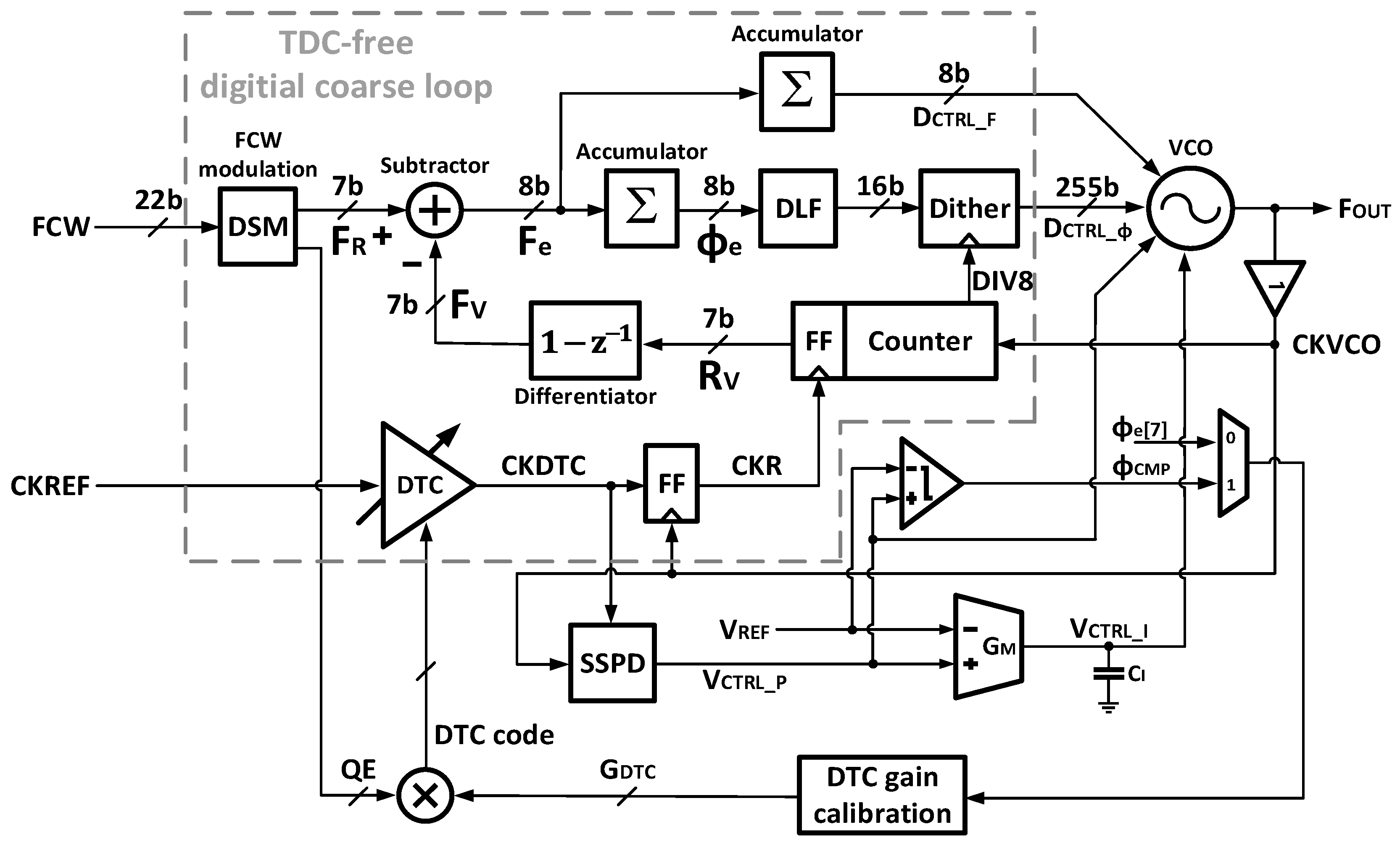
Figure 1 shows the overall block diagram of the proposed sub-sampling PLL. The proposed PLL adopts a dual-loop architecture comprising a digital coarse loop and an analog fine loop. The coarse loop employs a counter-assisted DPLL that, unlike conventional divider-based DPLLs, dispenses with the divider and uses a transition counter to count the number of VCO clock (CKVCO) rising edges within one period of the reference clock (CKREF). This provides a digital estimate of phase, which is compared with the integrated FCW to produce a digital phase error code [
9]. Compared with divider-based DPLLs, this approach avoids shaped quantization noise and being digital-intensive, benefits from the speed and scaling of advanced CMOS nodes. In this work, a differentiator is inserted in the feedback path of the counter-assisted DPLL to convert the VCO phase code R
V into a frequency code F
V; comparing F
V with the reference FCW yields a frequency-error code F
e. An additional integrator inside the coarse loop forms an auxiliary FLL path, enabling fast frequency convergence during initial acquisition. Once the frequency is quickly settled, the same counter-assisted framework transitions to phase locking: the frequency error F
e is routed through an integrator and a digital loop filter (DLF) along the PLL path to complete lock.
The fine loop adopts an analog SSPLL structure. It comprises a VCO isolation buffer, an SSPD that converts the phase difference between CKDTC and CKVCO into a proportional-path voltage VCTRL_P, a voltage-to-current converter (GM) with an integrating capacitor CI, a comparator, and the DTC, DSM, and VCO shared with the coarse loop. In conventional sampling PLLs, a differential-phase topology is often used to suppress common-mode noise and improve sampling accuracy. However, if the time-to-voltage slope of the two paths is not perfectly symmetric, fixed spurs arise. Moreover, to suppress sampler-induced feedthrough and Binary frequency-shift keying (BFSK)-like effects, a VCO buffer is required; yet inserting the buffer tends to make the voltage slopes excessively large, necessitating a ramp generator. Implementing two ramp generators for the differential-phase symmetrically is technically challenging due to rising/falling edge timing differences and circuit imbalance. For these reasons, the proposed design adopts a single-phase topology, which avoids symmetry issues and allows the lock point to be selected simply by setting the reference voltage, easing the DC biasing of the comparator and GM.
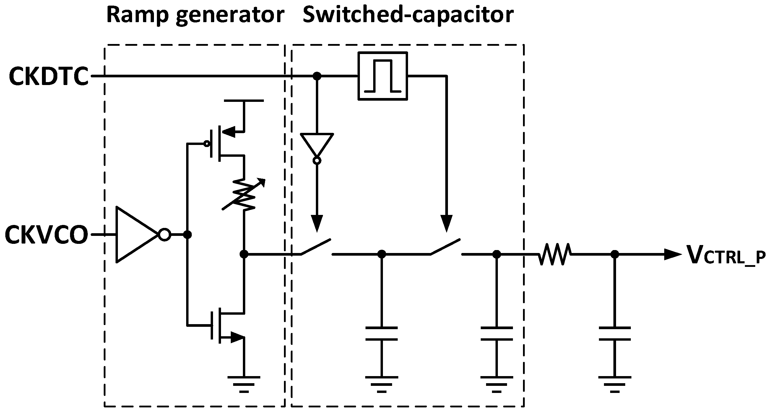
Figure 2 shows the circuit of the designed SSPD. In the fine loop, the SSPD is the key block that detects phase error by converting the time difference between CKDTC and CKVCO into voltage. A higher SSPD gain K
SSPD (output voltage per input phase) lowers the in-band PN of the PLL, improving jitter performance. The gain is set by the voltage slope of the ramp generator K
SLOPE as
The in-band PN contribution of the PD/CP can be expressed as an equivalent noise power spectral density (PSD). Using the transconductance
of the GM cell, Boltzmann constant
, and absolute temperature
, it is given by
Substituting the design values and (with and ) yields , i.e., a very high SSPD gain. Consequently, the in-band noise floor due to the SSPD is calculated to be about −160 dBc/Hz or lower, indicating that the SSPD noise does not limit the PN performance of the fine loop and enables low-PN operation.
However, an SSPD with such high gain is extremely sensitive to input phase error and therefore exhibits a narrow locking range. To hand over control between the coarse and fine loops without instability, the coarse loop must achieve a phase lock as precise as possible. In a conventional counter-assisted DPLL, a TDC is typically employed to reach this precision, but the required high resolution and linearity, together with a conversion range matched to the VCO period, increases circuit complexity and design burden. Moreover, when a DTC is used—as in this SSPLL—an inaccurate DTC gain prevents effective cancelation of DSM-induced quantization error (QE), so the input phase error of the SSPD cannot be kept near zero; with a very narrow locking range, such gain mismatch can even cause the fine loop to fail to converge. To solve the problems simultaneously, the fine loop reuses the DSM and DTC of fine loop and converts the reference path into an integer sequence by DSM-based FCW modulation, achieving precise phase locking without a TDC. In addition, an LMS-based DTC gain calibration is enabled in the coarse stage so that the gain reaches its target and is handed off directly to the fine loop, enabling stable loop switching despite the high SSPD gain. A further benefit is that the VCO phase information accumulated by the counter is processed entirely in the integer domain, allowing the subtractor and integrator to be realized with integer bits only, which simplifies hardware and reduces active area.
3. DSM-Based FCW Modulation
As noted in the previous section, the SSPD in fine loop has a constrained locking range due to its high PD gain. To enable a stable handover from the coarse loop to the fine loop, the fractional-N error should be pre-canceled in the integer domain of the coarse loop. Accordingly, this section proposes (i) converting the FCW into a variable integer sequence via a DSM and (ii) aligning integer-domain grids of the two paths by DTC-based retiming.
In a conventional counter-assisted DPLL, a retimed clock CKR is generated by sampling CKREF with CKVCO so that the number of VCO rising edges within one CKREF period can be counted reliably. Directly sampling the transition counter, which runs in the VCO domain at CKREF timing, would otherwise risk metastability and timing violations due to clock asynchrony; if a CKREF rising edge occurs near a CKVCO rising edge, the counter output can be latched mid-transition and produce an erroneous code [
10]. Beyond this practical necessity, the retiming can be interpreted as a quantization of the VCO path: because CKR aligns each CKREF event to the next VCO rising edge, the measured F
V at every CKR cycle is confined to an integer-domain grid. Hence, in the absence of a TDC, F
V appears as an integer-only, periodically varying sequence at steady state. By contrast, the reference frequency code F
R is fixed as same as the FCW that is composed of integer part FCW
int and fractional part FCW
frac; therefore, each quantization of F
V inevitably produces a fractional error code, leading to a mismatch between F
V and F
R in steady state that becomes a dominant source of residual phase error.
Figure 3 illustrates a block diagram of the proposed DSM-based integer FCW modulation. The DSM modulates FCW
frac into an integer sequence D[k] at each rising edge of CKR indexed by k. The reference frequency code F
R is then redefined as
The sequence D[k] is constructed as its long-term average equals FCWfrac; hence, the time average of FR[k] equals the original FCW. Because FR[k] is quantized by the DSM so that is integer-only rather than a fixed constant, comparing it with FV causes no fractional mismatch error.
Both F
R and F
V are expressed as integers by the DSM-based FCW modulation; however, their quantization mechanisms are different. Specifically, F
R is quantized by DSM, whereas F
V is quantized by CKR retiming.
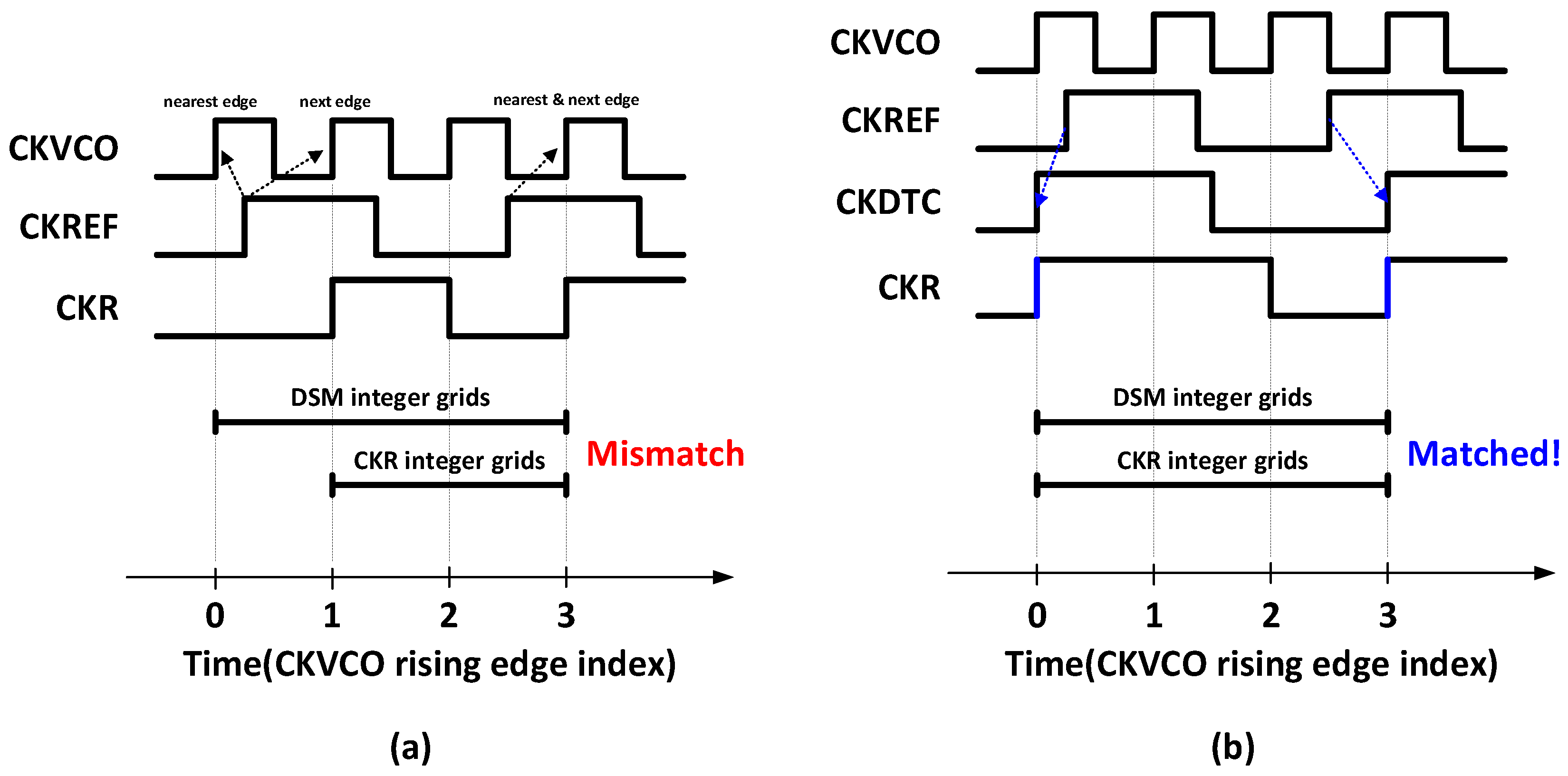
Figure 4a conceptually depicts the timing of this integer-domain operation when CKR is generated by retiming CKREF. In this case, the DSM performs quantization with respect to the VCO rising edge nearest to each CKREF rising edge, so F
R assumes values set by the DSM integer-grid. By contrast, CKR retiming aligns each CKREF event to the next VCO rising edge, so F
V follows the CKR integer-grid offset. As a result, a mismatch between F
V and F
R reappears.
To fix this mismatch, the quantization of F
V must occur on the same VCO rising edge used by the DSM. Therefore, CKR is now generated by retiming CKDTC with CKVCO instead of retiming CKREF. Because DTC removes the DSM-computed quantization error (QE), CKDTC is aligned to the VCO rising edge nearest each CKREF event. When CKR is derived from CKDTC, CKR is aligned to the same CKVCO edge designated by the DSM, and the quantization of F
V is performed on those identical edges.
Figure 4b conceptually illustrates this integer-domain timing: unlike
Figure 4a, CKR retiming uses CKDTC, so F
V assumes the same integer-grid offset as F
R. Finally, F
R and F
V are quantized under same integer-grids, and the error F
e = F
R − F
V converges to zero at steady state, enabling precise phase alignment in the coarse stage without a TDC.
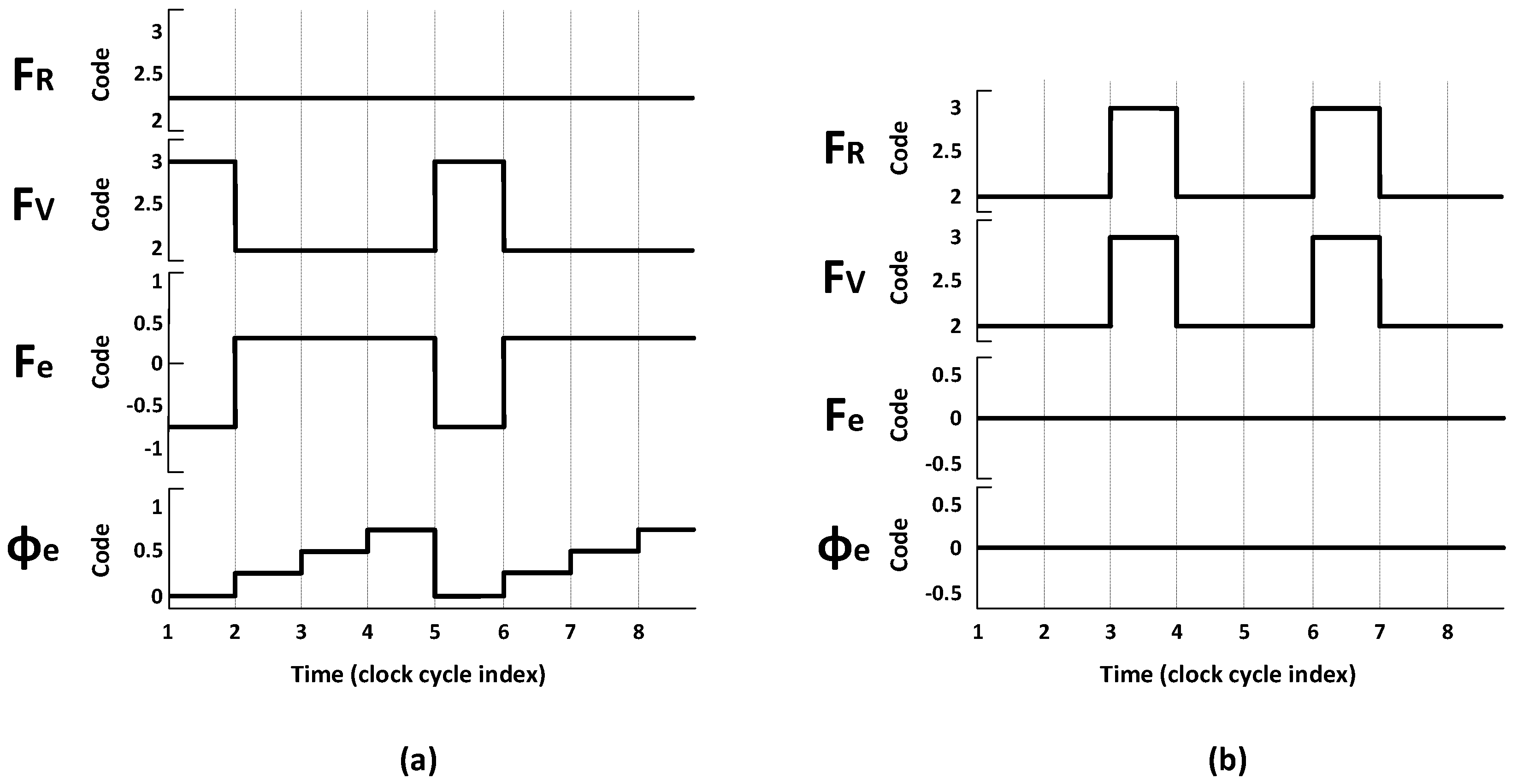
Figure 5 illustrates coarse-loop error detection for FCW = 2.25, comparing cases (a) without and (b) with DSM-based integer FCW modulation. In
Figure 5a, F
R is fixed at 2.25 containing both integer and fractional parts, whereas F
V is a periodically varying integer sequence due to CKR retiming; thus, the error F
e = F
R − F
V does not converge to zero and the phase error Φ
e exhibits stair-like values. In contrast to
Figure 5a, in
Figure 5b, the DSM modulates the FCW into an integer sequence F
R[k]; with DTC-based retiming, F
V is aligned to the same integer-domain grid, so F
e and Φ
e are held at zero in steady state.
In summary, the proposed method (i) quantizes the FCW by using a DSM to modulate its fractional part into a time-varying integer sequence, (ii) unifies the integer-domain grids of the two paths by shifting the reference edge with a DTC, and (iii) achieves precise phase lock without a TDC via the steady-state convergence of Fe to zero. Because any DTC gain deviation maps directly to grid misalignment, a background gain calibration loop is essential; its implementation is detailed in the next section.
4. DTC Gain Calibration
Building on the integer FCW modulation and DTC retiming of the previous section, the coarse loop achieves zero Fe at steady state. To preserve this alignment across the operating range and hand over control to the high-gain fine loop without instability, it is essential to rapidly converge and maintain the DTC gain GDTC during the coarse stage and continuously carry its value into the fine loop. This section explains the role of DTC gain calibration in the proposed architecture, specifies the stage-wise requirements for the coarse loop and fine loop, and presents a calibration loop that meets these requirements. DTC generates the time delay corresponding to the DSM-computed quantization error (QE), aligning CKDTC to the CKVCO edge designated by the DSM. If GDTC is erroneous, the QE compensation becomes under- or over-scaled, leaving integer-grid misalignment and preventing Fe from remaining at zero. In the fine loop, any GDTC error likewise hinders removal of fractional-N error and can induce unstable behavior at the SSPD output due to its narrow locking range. Therefore, (i) in the coarse stage, GDTC must be driven quickly to its target to satisfy loop-switching conditions, and (ii) in the fine stage, calibration must proceed with a narrow bandwidth to minimize residual error and spurs.
The optimal value of G
DTC is defined as follows: the actual time delay corresponding to the QE is
To compensate for QE, a DTC with single-LSB time resolution
produces a delay
Introducing the scale factor DTC gain G
DTC,
so that
The alignment condition requires that
which yields the proportionality constant that maps the digital code to physical time delay:
When this relation holds, DTC generates the correct time delay proportional to QE, aligns CKDTC to the nearest rising edge of CKVCO, and thereby cancels the quantization error in the time domain.
Due to this process, supply voltage, and temperature (PVT) variations, the DTC unit delay
deviates from its design value and drifts over time; hence, background DTC gain calibration is essential for robust operation. An LMS-based scheme is adopted that incrementally updates the current G
DTC from the correlation between the signs of the DSM QE and the loop error, and the calibration is divided into coarse and fine stages to achieve, respectively, fast convergence and high precision. The update of coarse stage is
where
sets the calibration bandwidth,
denotes the sign function, and Φ
e,n is the digital phase error at iteration
n. To drive G
DTC rapidly toward its target, a relatively large
is chosen; however, if
is too large and the coarse stage calibration bandwidth exceeds the bandwidth of the coarse loop, the calibration loop can become unstable and the residual gain error may produce a fractional error outside the locking range of the SSPD. Thus,
is selected considering the bandwidth of the coarse loop and the SSPD lock range. After G
DTC has converged to its optimum value and Φ
e,n remains within a preset threshold for ≥63 digital clock cycles, the system declares convergence of the coarse loop and performs handover to the fine loop. The update of the fine stage is
where Φ
cmp,n is the phase polarity signal of the fine loop derived by the comparator and small
narrows the fine stage calibration bandwidth to refine G
DTC. A too small
prolongs the removal of residual error, so it is chosen with lock time in mind. With this fine stage calibration, the G
DTC handed off from the coarse stage is tightly trimmed, reducing fractional error in the fine loop and minimizing spur and jitter sensitivity to gain drift.
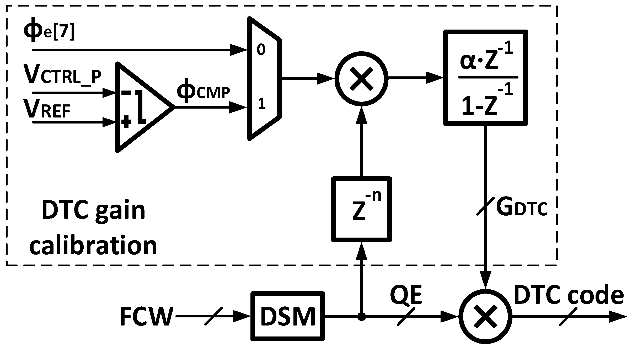
Figure 6 depicts the block diagram of the DTC gain calibration. The loop implements an LMS-based correlation algorithm and operates in two stages. In the coarse stage, the input is the digital phase error of the coarse loop Φ
e. In the fine stage, the input is the comparator output Φ
cmp, which represents the polarity of the phase error of fine loop. A MUX selects between these two signals according to the active stage, and the adaptation step sizes
and
are programmed for the coarse and fine stages, respectively.
In summary, this hierarchical LMS calibration drives GDTC rapidly to its optimum, removing the DSM-induced QE, improving accuracy of phase detection in both loops, and ensuring robust coarse-to-fine loop switching.
5. Simulation Results
Section 5 presents the implementation and simulation results of the proposed PLL. The circuit was implemented in a 28 nm CMOS process (Samsung 28 nm LPP CMOS) using the Cadence Virtuoso environment. Post-layout parasitics were extracted with Synopsys StarRC and included in the simulations. Mixed-signal behavior was verified using the Cadence AMS flow with Specter for the analog parts and Verilog models for the digital logic. Figures 8 and 9 present post-layout transient simulation results including the extracted parasitics. For the system-level verification and calibration analysis in Figures 10 and 11, the transistor-level analog circuits were replaced by behavioral models while keeping the digital logic unchanged; these simulations were also carried out in the Cadence AMS environment. All waveform data used to generate Figures 8–11 were exported from the simulator and post-processed in MATLAB to produce the plotted results.
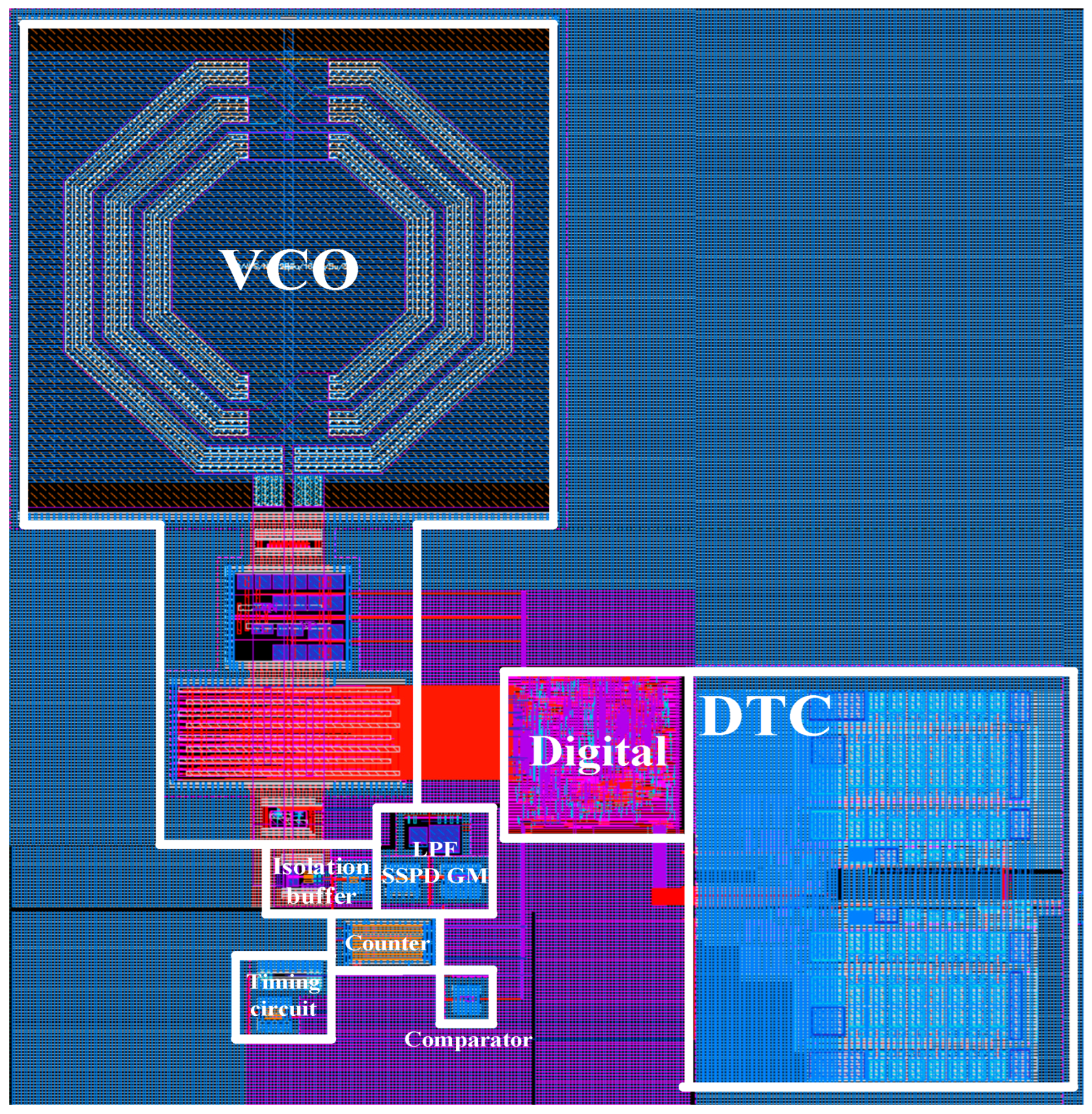
Figure 7 shows the layout of the PLL implemented in a 28 nm CMOS process. The PLL operates over 4–5 GHz with an active area of 0.146 mm
2. At a 104 MHz reference, the fine loop consumes 8.94 mW.
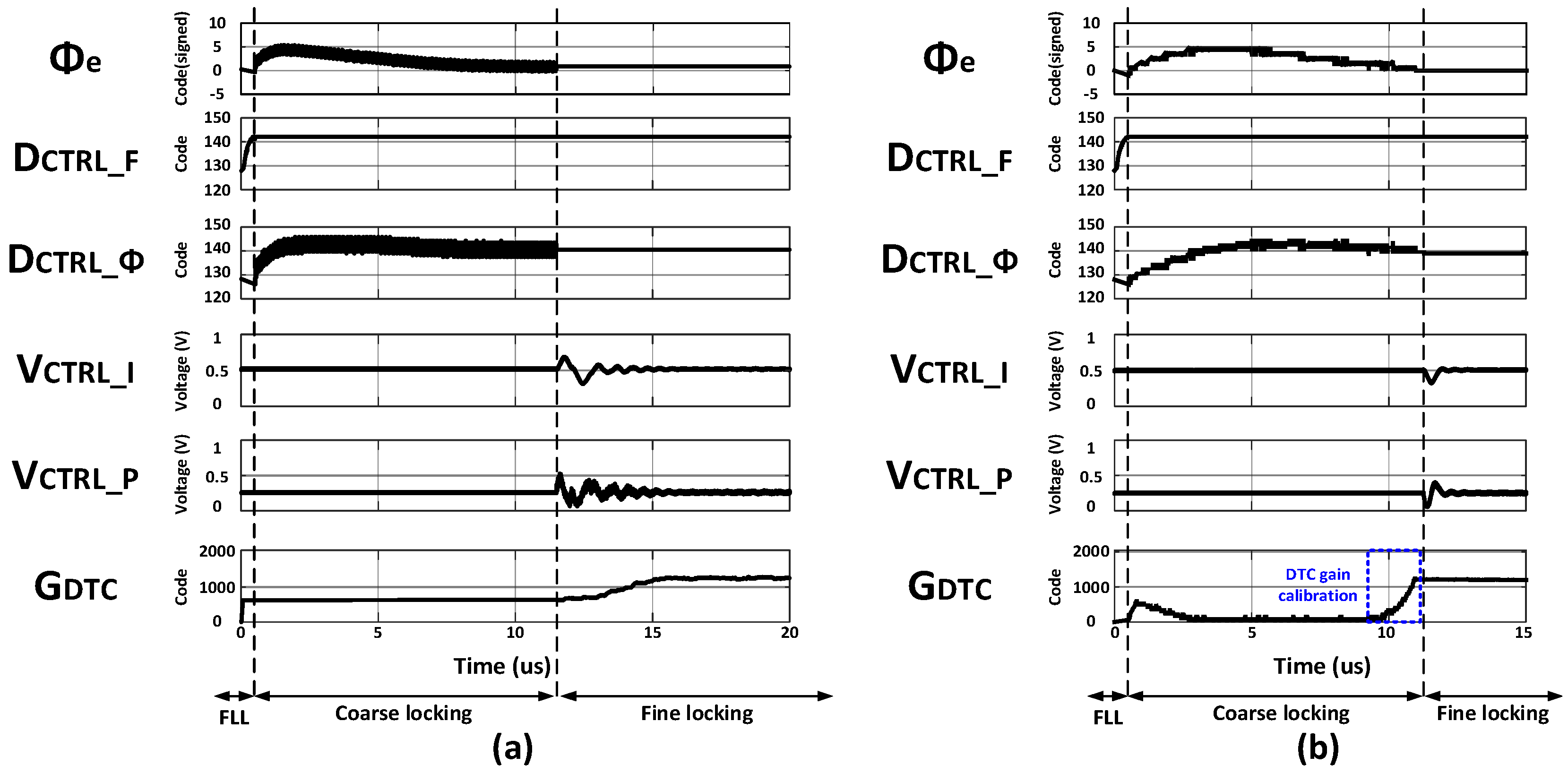
Figure 8 presents post-layout transient simulation results that visualize phase locking and calibration of the overall PLL.
Figure 8a shows the case without DSM-based FCW modulation. Here, the reference path code F
R remains fixed to the FCW (containing both integer and fractional parts), whereas the variable path code F
V is quantized by reference retiming. Consequently, the error F
e = F
R − F
V does not converge to zero, and the accumulated phase error Φ
e exhibits a staircase profile at steady state. The coarse-loop control code D
CTRL_Φ therefore fails to settle precisely, and fine phase locking is not achieved. In addition, because no DTC gain calibration runs in the coarse loop, G
DTC cannot reach its optimum; the resulting input error can exceed locking range of the SSPD. After handover to the fine loop, V
CTRL_I and V
CTRL_P do not settle promptly, requiring extra time for both phase alignment and DTC gain correction; the overall lock time is thus prolonged.
Figure 8b shows the case with DSM-based FCW modulation. Unlike
Figure 8a, the coarse loop quantizes F
R via DSM and aligns it to the same integer-domain convention as F
V; as a result, F
e and Φ
e are held at zero in steady state. In parallel, G
DTC converges near its target already within the coarse loop and is handed off to the fine loop, keeping the SSPD input phase error small. Following handover, V
CTRL_I and V
CTRL_P settle within 1 µs, yielding a noticeably shorter lock time. In summary, DSM-based FCW modulation enables precise coarse-loop phase alignment and effective DTC gain calibration at the coarse stage, which together improve the stability of loop switching and reduce acquisition time.
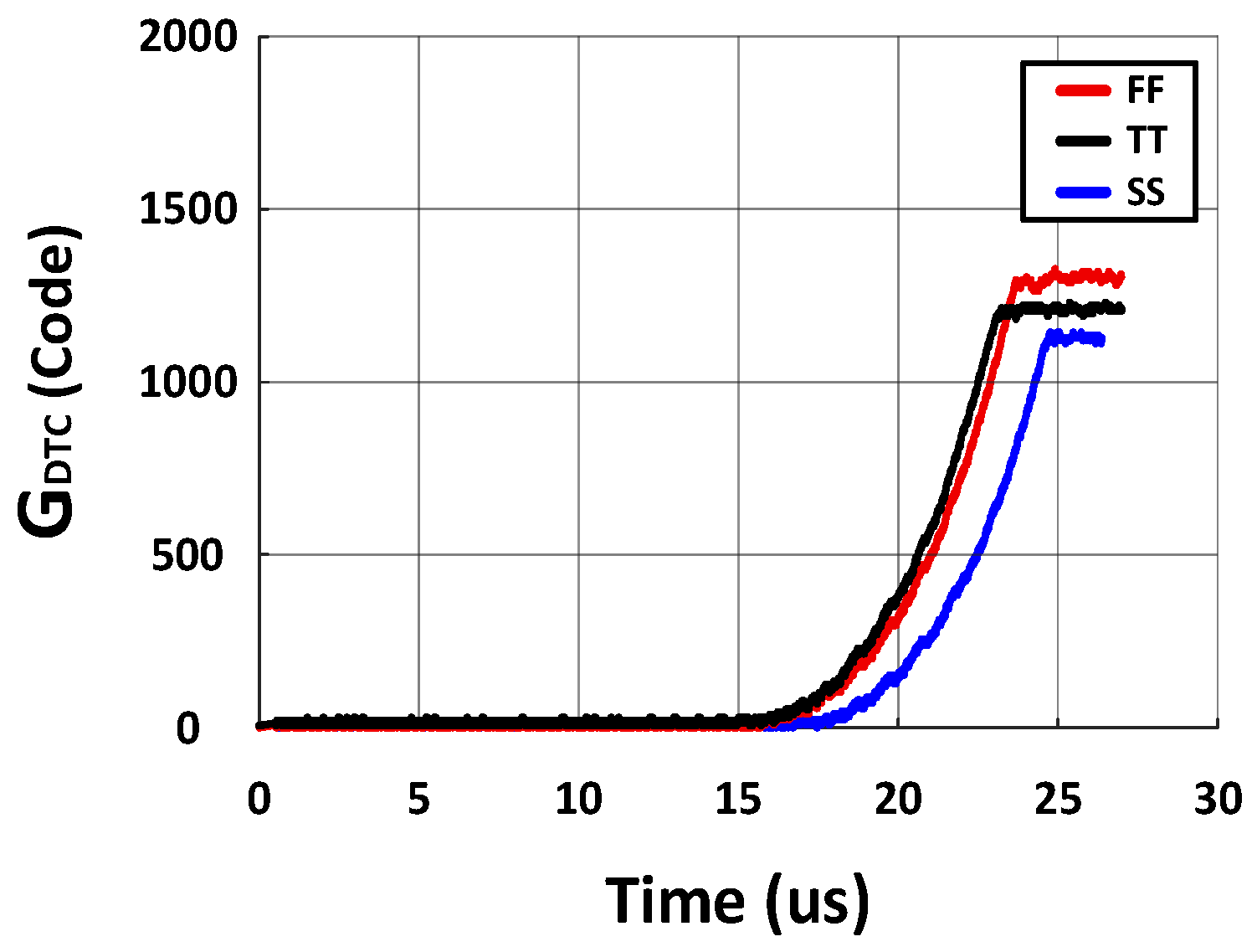
Figure 9 presents the post-layout transient results of the coarse-loop DTC gain calibration across CMOS process corners (SS, TT, FF). The ideal DTC gain, given by Equation (9), is
. With the VCO target frequency fixed at 4.5 GHz, the minimum delay of DTC (
) varies with the process corner; hence, G
DTC differs across SS/TT/FF—higher for smaller
and lower for larger
.
Figure 9 shows that the implemented PLL successfully calibrates the gain across all three corners.
The models used in the simulations for
Figure 10 and
Figure 11 were designed to operate in a manner closely matching the actual circuits based on design parameters. In particular, the time resolution corresponding to one least significant bit (LSB) of the DTC code, denoted as
, was set to the design value of 750 fs/LSB, and the DTC nonlinearity was incorporated into the model.
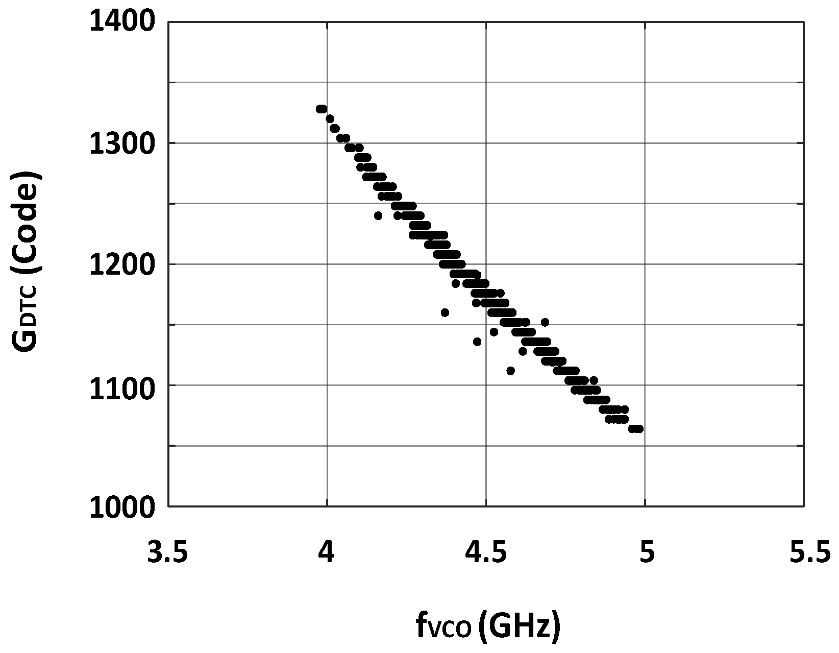
Figure 10 presents the DTC gain calibration results obtained from modeling simulations in the coarse loop. As shown in
Figure 10, the converged G
DTC values are distributed almost linearly with respect to the VCO operating frequency, indicating that the condition of Equation (9) was satisfied and the DTC gain was accurately calibrated across the entire PLL operating range through coarse loop gain calibration alone.
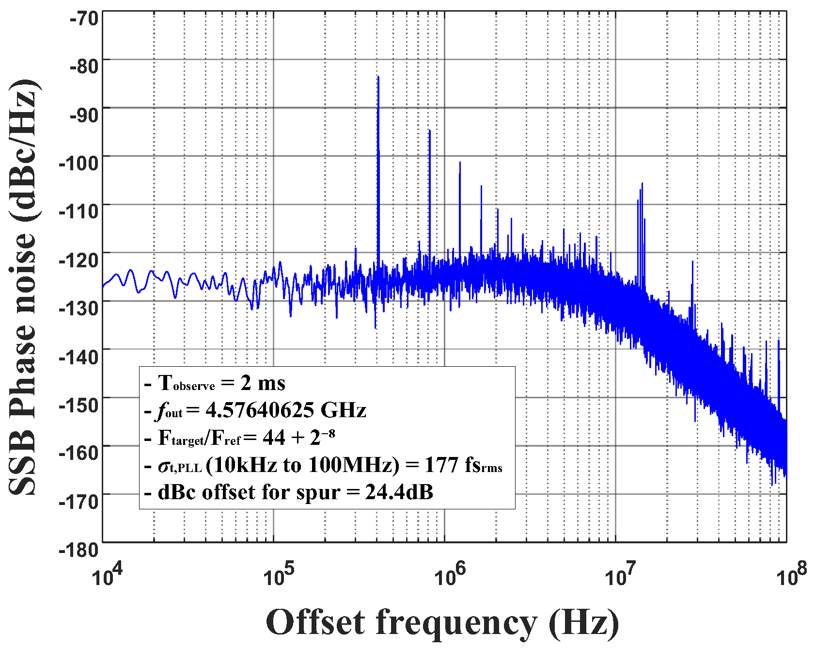
Figure 11 shows the simulated PN spectrum of the proposed PLL using modeling. At the output frequency of 4.57640625 GHz (
), the integrated RMS jitter over the 10 kHz–100 MHz offset range was evaluated to be 177 fs,
RMS. This result demonstrates that the proposed fine loop achieves high performance with low jitter as designed.
Table 1 compares the performance of the proposed PLL with that of recently reported LC-VCO-based analog PLLs. The proposed PLL achieved a FoM regarding PN (FoM
PN) of –245.6 dB and an area-normalized FoM (FoM
Area) of –254 dB, confirming that the area efficiency of this work is competitive among state-of-the-art analog PLLs.
6. Conclusions
This work presented a 4–5 GHz SSPLL that integrates a TDC-free digital coarse loop with a high-gain SSPD fine loop. The counter-assisted frequency-domain structure of the coarse loop, augmented by an FLL path, provides rapid initial frequency acquisition. By reusing DSM and DTC in the coarse loop—DSM for integer-domain FCW modulation and DTC for time-domain alignment on the same quantization grid—the phase error of the coarse loop is driven to zero in steady state, enabling precise fractional-N synthesis without a TDC. A hierarchical LMS-based DTC gain calibration operates in the coarse and fine loop, and the calibrated GDTC is handed off to the fine loop, yielding fast gain convergence and stable loop switching even with narrow locking range of the SSPD. Simulations of a 28 nm CMOS implementation confirm 0.146 mm2 active area, 8.94 mW power, and 177 fs RMS jitter, indicating high performance per area and reliable operation across the target band. Future directions include nonlinearity compensation of the DTC to further reduce fractional spurs and long-term robustness studies under on-chip temperature/voltage variations and aging, as well as silicon validation of the proposed architecture.
Author Contributions
Conceptualization, J.J. and S.K.; methodology, J.J. and S.K.; validation, J.J. and S.K.; formal analysis, J.J., Y.K. and S.K.; data curation, J.J. and S.K.; writing—original draft preparation, J.J., Y.K. and S.K.; writing—review and editing, Y.K. and S.K.; visualization, J.J. and S.K.; supervision, S.K.; project administration, S.K. All authors have read and agreed to the published version of the manuscript.
Funding
This work was supported by the BK-21 FOUR program through the National Research Foundation of Korea (NRF) under the Ministry of Education.
Data Availability Statement
The original contributions presented in this study are included in the article. Further inquiries can be directed to the corresponding author.
Acknowledgments
The EDA tool was supported by the IC Design Education Center (IDEC), Korea.
Conflicts of Interest
The authors declare no conflicts of interest.
Abbreviations
The following abbreviations are used in this manuscript:
| 5G NR | 5G New Radio |
| BFSK | Binary frequency-shift keying |
| DPLL | Digital phase-locked loop |
| DSM | Delta–sigma modulator |
| DTC | Digital-to-time converter |
| EVM | Error vector magnitude |
| FCW | Frequency control word |
| FLL | Frequency-locked loop |
| FoM | Figure of merit |
| GM | Voltage-to-current converter |
| ILCM | Injection-locked clock multiplier |
| ISAC | Integrated sensing and communications |
| LMS | Least-mean-square |
| LOs | Local oscillators |
| LSB | Least significant bit |
| mMTC | Massive machine-type communications |
| NA | Not available |
| PD | Phase detector |
| PFD–CP | Phase–frequency detector/charge pump |
| PLL | Phase-locked loop |
| PN | Phase noise |
| PSD | Power spectral density |
| PVT | Process, supply voltage, and temperature |
| QE | Quantization error |
| RMS | Root mean square |
| SSPD | Sub-sampling phase detector |
| SSPLL | Sub-sampling phase-locked loop |
| TDC | Time-to-digital converter |
| URLLC | Ultra-reliable and low-latency communications |
| V2X | Vehicle-to-everything |
| VCO | Voltage-controlled oscillator |
References
- Garcia, M.H.C.; Molina-Galan, A.; Boban, M.; Gozalvez, J.; Coll-Perales, B.; Şahin, T.; Kousaridas, A. A Tutorial on 5G NR V2X Communications. IEEE Commun. Surv. Tutor. 2021, 23, 1972–2026. [Google Scholar] [CrossRef]
- Akpakwu, G.A.; Silva, B.J.; Hancke, G.P.; Abu-Mahfouz, A.M. A Survey on 5G Networks for the Internet of Things: Communication Technologies and Challenges. IEEE Access 2018, 6, 3619–3647. [Google Scholar] [CrossRef]
- Ghosh, A.; Maeder, A.; Baker, M.; Chandramouli, D. 5G Evolution: A View on 5G Cellular Technology Beyond 3GPP Release 15. IEEE Access 2019, 7, 127639–127651. [Google Scholar] [CrossRef]
- Foukas, X.; Patounas, G.; Elmokashfi, A.; Marina, M.K. Network Slicing in 5G: Survey and Challenges. IEEE Commun. Mag. 2017, 55, 94–100. [Google Scholar] [CrossRef]
- Wu, W.; Yao, C.-W.; Godbole, K.; Ni, R.; Chiang, P.-Y.; Han, Y.; Zuo, Y.; Verma, A.; Lu, I.S.-C.; Son, S.W.; et al. A 28-nm 75-fsrms Analog Fractional-N Sampling PLL With a Highly Linear DTC Incorporating Background DTC Gain Calibration and Reference Clock Duty Cycle Correction. IEEE J. Solid-State Circuits 2019, 54, 1254–1265. [Google Scholar] [CrossRef]
- Liu, F.; Cui, Y.; Masouros, C.; Xu, J.; Han, T.X.; Eldar, Y.C.; Buzzi, S. Integrated Sensing and Communications: Toward Dual-Functional Wireless Networks for 6G and Beyond. IEEE J. Sel. Areas Commun. 2022, 40, 1728–1767. [Google Scholar] [CrossRef]
- Gao, X.; Klumperink, E.A.M.; Bohsali, M.; Nauta, B. A Low Noise Sub-Sampling PLL in Which Divider Noise is Eliminated and PD/CP Noise is Not Multiplied by N2. IEEE J. Solid-State Circuits 2009, 44, 3253–3263. [Google Scholar] [CrossRef]
- Li, H.; Xu, T.; Meng, X.; Yin, J.; Martins, R.P.; Mak, P.-I. A 23.2-to-26-GHz Low-Jitter Fast-Locking Sub-Sampling PLL Based on a Function-Reused VCO-Buffer and a Type-I FLL With Rapid Phase Alignment. IEEE J. Solid-State Circuits 2024, 59, 3952–3965. [Google Scholar] [CrossRef]
- Tokairin, T.; Okada, M.; Kitsunezuka, M.; Maeda, T.; Fukaishi, M. A 2.1-to-2.8-GHz Low-Phase-Noise All-Digital Frequency Synthesizer With a Time-Windowed Time-to-Digital Converter. IEEE J. Solid-State Circuits 2010, 45, 2582–2590. [Google Scholar] [CrossRef]
- Staszewski, R.B.; Balsara, P.T. Phase-domain all-digital phase-locked loop. IEEE Trans. Circuits Syst. II Express Briefs 2005, 52, 159–163. [Google Scholar] [CrossRef]
- Song, F.; Zhao, Y.; Wu, B.; Tang, L.; Lin, L.; Razavi, B. 16.5 A Fractional-N Synthesizer with 110fsrms Jitter and a Reference Quadrupler for Wideband 802.11ax. In Proceedings of the 2019 IEEE International Solid-State Circuits Conference (ISSCC), San Francisco, CA, USA, 17–21 February 2019. [Google Scholar]
- Elkholy, A.; Elmallah, A.; Ahmed, M.G.; Hanumolu, P.K. A 6.75–8.25-GHz−250-dB FoM Rapid ON/OFF Fractional-N Injection-Locked Clock Multiplier. IEEE J. Solid-State Circuits 2018, 53, 1818–1829. [Google Scholar] [CrossRef]
- Markulic, N.; Raczkowski, K.; Martens, E.; Filho, P.E.P.; Hershberg, B.; Wambacq, P.; Craninckx, J. A DTC-Based Subsampling PLL Capable of Self-Calibrated Fractional Synthesis and Two-Point Modulation. IEEE J. Solid-State Circuits 2016, 51, 3078–3092. [Google Scholar] [CrossRef]
| Disclaimer/Publisher’s Note: The statements, opinions and data contained in all publications are solely those of the individual author(s) and contributor(s) and not of MDPI and/or the editor(s). MDPI and/or the editor(s) disclaim responsibility for any injury to people or property resulting from any ideas, methods, instructions or products referred to in the content. |
© 2025 by the authors. Licensee MDPI, Basel, Switzerland. This article is an open access article distributed under the terms and conditions of the Creative Commons Attribution (CC BY) license (https://creativecommons.org/licenses/by/4.0/).
