Article

A Multi-Mode Wireless Power Transfer System Based on a Reconfigurable Transmitter for Charging Electric Bicycles

1
College of Information Technology, University of New South Wale, Sydney, NSW 2052, Australia
2
School of Electrical and Electronic Engineering, Harbin University of Science and Technology, Harbin 150080, China
*
Author to whom correspondence should be addressed.
Electronics 2025, 14(21), 4315; https://doi.org/10.3390/electronics14214315
Submission received: 10 October 2025 / Revised: 31 October 2025 / Accepted: 31 October 2025 / Published: 3 November 2025
(This article belongs to the Special Issue Wireless Power Transfer and Hybrid Energy Harvesting)

Abstract

Due to the diverse needs of users, such as the requirement for rapid charging in time-sensitive situations and the need to minimize battery power consumption to extend battery life when the device is idle, a wireless charging system that combines fast and slow charging capabilities is crucial for adapting to various usage scenarios. This paper proposes a multi-mode wireless charging system based on a reconfigurable transmitter, which can simultaneously charge different types of batteries with both fast and slow charging capabilities. By applying different control logic to the power devices in the reconfigurable inverter, the system can achieve four operating modes: two different constant current (CC) modes and two different constant voltage (CV) modes. Furthermore, the system can switch between these modes by configuring the MOSFETs operating states: two three-coil configurations are used for the two CC modes, while two two-coil configurations are used for the two CV modes. Therefore, the system exhibits high versatility. To verify the theoretical analysis of the proposed system, an experimental prototype with an output specification of 3 A/2.2 A/78 V/65 V is built.

1. Introduction

Compared to traditional wired charging methods that rely on physical cable connections, wireless power transfer (WPT) offers advantages such as higher safety, electrical isolation, and ease of maintenance, as it enables energy transmission without any physical connection [1,2,3]. Due to these advantages, WPT technology has been applied in many fields, such as electric vehicles [4,5,6], biomedical devices [7,8,9], automated guided vehicles [10,11], and other industrial applications [12,13,14]. Today, electric bicycles, with their environmentally friendly and convenient features, have gradually become an essential means of transportation. However, the safety issues related to charging electric bicycles have become a major research challenge, and therefore, charging methods based on wireless power transfer (WPT) technology are gradually gaining popularity.
Electric bicycles typically use environmentally friendly, high-capacity lithium-ion batteries as their power source. To extend battery life during the charging process, the charging stage needs to follow a two-step process: first constant current (CC) charging, followed by constant voltage (CV) charging, in accordance with the ideal charging curve for lithium-ion batteries [15,16]. Furthermore, the equivalent resistance of the battery inevitably changes significantly during the charging process. Therefore, achieving CC and CV output independent of the load is a crucial performance indicator for a WPT system.
With this as a foundation, three control methods, namely Phase Shift Control (PSC) [17,18], Frequency Control (FCC) [19,20], and DC-DC Auxiliary Control (DDAC) [21,22], have been put forward by researchers. Among them, PSC achieves CC and CV output by controlling the phase difference angle of the power converter on the transceiver side. However, this method cannot achieve zero-voltage switching (ZVS) when the load variation range is large, thus leading to significant switching losses. In Refs. [19,20], because the output characteristics of a WPT system are related to the operating frequency, researchers have used a frequency control method (FCC) that continuously adjusts the system frequency to maintain constant output characteristics under varying load conditions. However, this method prevents the system from operating at zero phase angle (ZPA), resulting in increased reactive power losses. Based on the shortcomings of the two control methods mentioned above, references [21,22] proposed using a DC-DC converter to achieve a constant output, offering a wider control range and avoiding the instability caused by real-time frequency adjustment. However, while DDAC provides a relatively stable solution for achieving a constant output, the additional converter increases the number of redundant components and the overall system cost. In summary, although all three control methods can meet the requirement for a constant output, they all suffer from issues such as complex control and high cost.
To overcome the limitations of the three control methods mentioned above, researchers have proposed a hybrid topology scheme. This scheme utilizes the inherent structural characteristics of the topology, integrating topologies with different output characteristics through the addition of extra AC switches, thus enabling selective output of either CC or CV characteristics. Qu et al. [23] proposed a method to achieve CC to CV conversion by controlling AC switches on the transmitter side to perform topology transformation. However, this method inevitably requires adding a Bluetooth communication module between the receiver and transmitter, which increases the complexity of system control. To avoid the impact of Bluetooth communication on the system, Li et al. [24] proposed a hybrid topology circuit that eliminates the need for Bluetooth communication. This method achieves topology switching by adding an AC switch on the receiver side. However, the design requirements for WPT systems necessitate a lightweight receiver design, while the method in ref. [24] undoubtedly requires adding redundant components to the receiver. Therefore, Mai et al. [25] and Vu et al. [26] used a single topology, but varied the operating frequency of the system to achieve different types of output characteristics. However, because the method described in ref. [25] uses a low-order compensation topology with an SS topology, it has limited resonant frequency points, which prevents it from achieving ZPA operation in CV mode, resulting in a significant decrease in system efficiency. Therefore, the high-order LCC-LCC compensation topology described in ref. [26] is adopted, which allows ZPA operation in both CC and CV modes.
In fact, different models of electric bicycles typically have different nominal voltages due to their varying battery configurations. Furthermore, to further save energy for users, the system should ideally include both fast and slow charging modes, providing users with more charging options. However, the wireless charging systems described in refs. [23,24,25,26] cannot provide multiple output currents and voltages to meet diverse charging needs. Ref. [27] proposes a system for wireless charging of electric bicycle batteries of different specifications. This system achieves multiple output voltages by configuring multiple compensation components with varying parameters at the receiver end. However, each output port of this system can still only provide a single output voltage; furthermore, adding each additional output channel requires an equivalent number of compensation components, which leads to a significant increase in system cost. Therefore, this system still fails to address the shortcomings mentioned in refs. [23,24,25,26].
Based on the shortcomings of the aforementioned methods, this paper proposes a multi-mode wireless charging system based on a reconfigurable transmitter, capable of simultaneously performing fast and slow charging for different types of batteries. By applying different control logic to the power devices in the reconfigurable inverter, the system can achieve four operating modes: two CC modes and two CV modes. Furthermore, by adjusting the operating state of the MOSFETs, the system can switch between these modes: the two CC modes utilize a three-coil structure, while the two CV modes use a two-coil structure. Therefore, this system offers high flexibility and versatility, making it well-suited for electric bicycle charging.

2. Theoretical Analysis

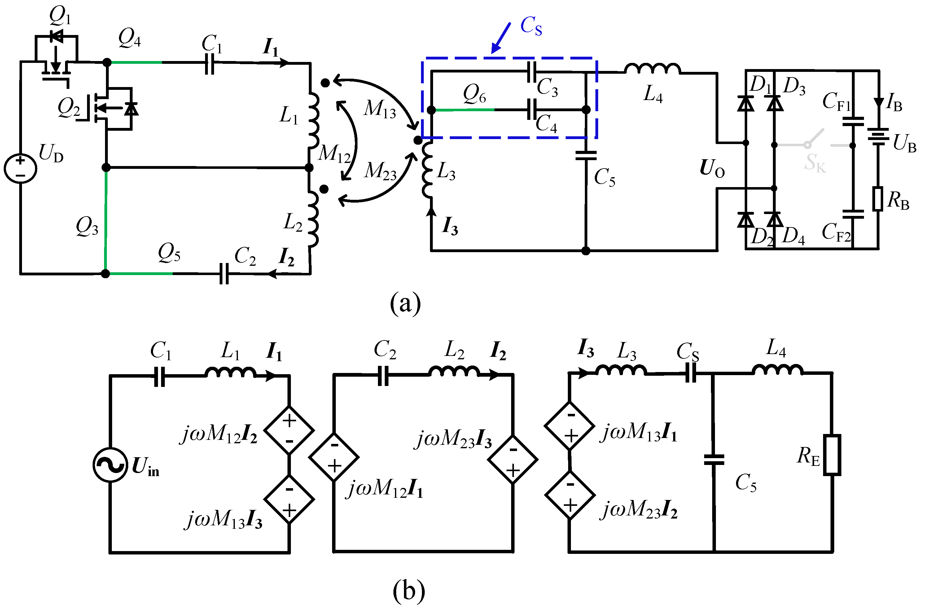
The overall architecture of the proposed dual-mode WPT system is shown in Figure 1. As evident from Figure 1, the transmitting side of the system includes two resonant circuits. Among them, the resonant circuit consisting of the first transmitting coil L 1 and the corresponding compensation capacitor C 1 is defined as Loop 1 and is covered by the pink shading. The resonant circuit consisting of the second transmitting coil L 2 and the compensation capacitor C 2 is defined as Loop 2 and is covered by the blue shading. In addition, the transmitter side also includes a reconfigurable inverter consisting of four MOSFETs ( Q 1 Q 5 ). The receiving side includes a receiving coil L 3 , a series compensation capacitor C 3 , a parallel compensation capacitor C 5 , and a series compensation inductor L 4 , forming an LCC compensation network. It’s worth noting that the series circuit of C 4 and Q 6 is connected in parallel with C 3 to match the resonant conditions in both two CC modes. Among them, the resonant circuit consisting of L 3 , C 3 , C 4 , C 5 , L 5 , and Q 6 is defined as Loop 3 and is covered by the yellow shading. The receiving side also includes a rectifier with efficiency improvement, consisting of four diodes ( D 1 D 4 ) and relay S K , a filter capacitor C F , and a battery-equivalent load RB. Furthermore, M 12 , M 13 , and M 23 are the mutual inductances between the three coils. I B and U B are the charging current and charging voltage of the battery, respectively.
Based on the reconfiguration characteristics of the inverter, the above system can be selectively configured into two S-S-LCC three-coil structures to achieve two CC modes and two S-LCC two-coil structures to achieve two CV modes by controlling the working state of the MOSFETs. The corresponding control logic is shown in Figure 2.
In addition, in order to ensure that the system outputs a constant voltage or current in the corresponding mode, different resonance conditions need to be matched. Therefore, the compensation capacitor in the system should satisfy the following expression [28].
C 1 = 1 ω L 1 2 C 2 = 1 ω L 2 2 C 3 = 1 ω L 3 L 4 2 C 5 = 1 ω L 4 2 C S = M 12 ω 2 L 3 L 4 L 3 L 4 M 12 2 M 13 M 23 C 4 = 2 M 13 M 23 ω 2 L 3 L 4 L 3 L 4 M 12 2 M 13 M 23

2.1. CC1 Mode

According to the control logic in Figure 2a, when the transmitter-side MOSFETs Q 1 and Q 2 operate alternately at a 50% duty cycle and Q 3 , Q 4 , and Q 5 are on, both Loop 1 and Loop 2 operate, and the equivalent inverter is suspended in Loop 1, acting as the transmitter circuit, while Loop 2 acts as the relay circuit. When the receiving-side MOSFET Q 6 is turned on, C 3 and C 4 are connected in parallel to form a C S , matching the resonant conditions in CC1 mode. At this point, the LCC compensation structure formed by C S , C 5 , and L 4 , along with transmitting coil L 3 , acts as the receiving circuit. To simplify the analysis, the equivalent circuit of the first S-S-LCC three-coil structure configured in CC1 mode is given, as shown in Figure 3b. As evident from Figure 3b, using Kirchhoff’s voltage law (KVL) can be used to obtain the equation is as follows.
U i n = j ω L 1 + 1 j ω C 1 I 1 + j ω M 12 I 2 j ω M 13 I 3 0 = j ω M 12 I 1 + j ω L 2 + 1 j ω C 2 I 2 j ω M 23 I 3 0 = j ω M 13 I 1 + j ω M 23 I 2 + j ω L 3 + 1 j ω C 5 + 1 j ω C S I 3 1 j ω C 5 I 4 0 = 1 j ω C 5 I 3 + j ω L 4 + 1 j ω C 5 + R E I 4
Substituting the resonant condition in Equation (1) and equation U in = 2 π U D for the half-bridge inverter into Equation (2), the first charging current I B 1 and input impedance Z i n in CC1 mode can be express as:
I B 1 = 2 2 π I 4 = 4 π 2 M 23 U D ω L 4 M 12 Z in = U in I 1 = π 2 ω 2 L 4 2 M 12 2 8 M 23 2 R B
As can be seen from (3), the first charging current I B 1 is independent of the variable battery load R B . Therefore, the system can achieve a CC output in CC1 mode. In addition, Z i n is purely resistive. In other words, the proposed system can achieve ZPA operation in CC1 mode.

2.2. CC2 Mode

According to the control logic in Figure 3b, when the transmitter-side MOSFETs Q 1 and Q 3 operate alternately at a 50% duty cycle and Q 2 , Q 4 , and Q 5 are on, both Loop 1 and Loop 2 operate, and the equivalent inverter is suspended in Loop 2, acting as the transmitter circuit, while Loop 1 acts as the relay circuit. Similar to CC1 mode, the LCC compensation structure formed by C S , C 5 , and L 4 , along with transmitting coil L 3 , acts as the receiving circuit. To simplify the analysis, the equivalent circuit of the second S-S-LCC three-coil structure configured in CC2 mode is given, as shown in Figure 4b. As evident from Figure 4b, using KVL can be used to obtain the equation is as follows.
0 = j ω L 1 + 1 j ω C 1 I 1 + j ω M 12 I 2 j ω M 13 I 3 U i n = j ω M 12 I 1 + j ω L 2 + 1 j ω C 2 I 2 j ω M 23 I 3 0 = j ω M 13 I 1 + j ω M 23 I 2 + j ω L 3 + 1 j ω C 5 + 1 j ω C S I 3 1 j ω C 5 I 4 0 = 1 j ω C 5 I 3 + j ω L 4 + 1 j ω C 5 + R E I 4
Substituting the resonant condition in Equation (1) and equation U in = 2 π U D for the half-bridge inverter into Equation (4), the second charging current I B 2 and input impedance Z i n in CC2 mode can be express as.
I B 2 = 2 2 π I 4 = 4 π 2 M 13 U D ω L 4 M 12 Z in = U in I 1 = π 2 ω 2 L 4 2 M 12 2 8 M 13 2 R B
As can be seen from (5), the second charging current I B 2 is independent of the variable battery load R B . Therefore, the system can achieve a CC output in CC2 mode. In addition, Z i n is purely resistive. In other words, the proposed system can achieve ZPA operation in CC2 mode.

2.3. CV1 Mode

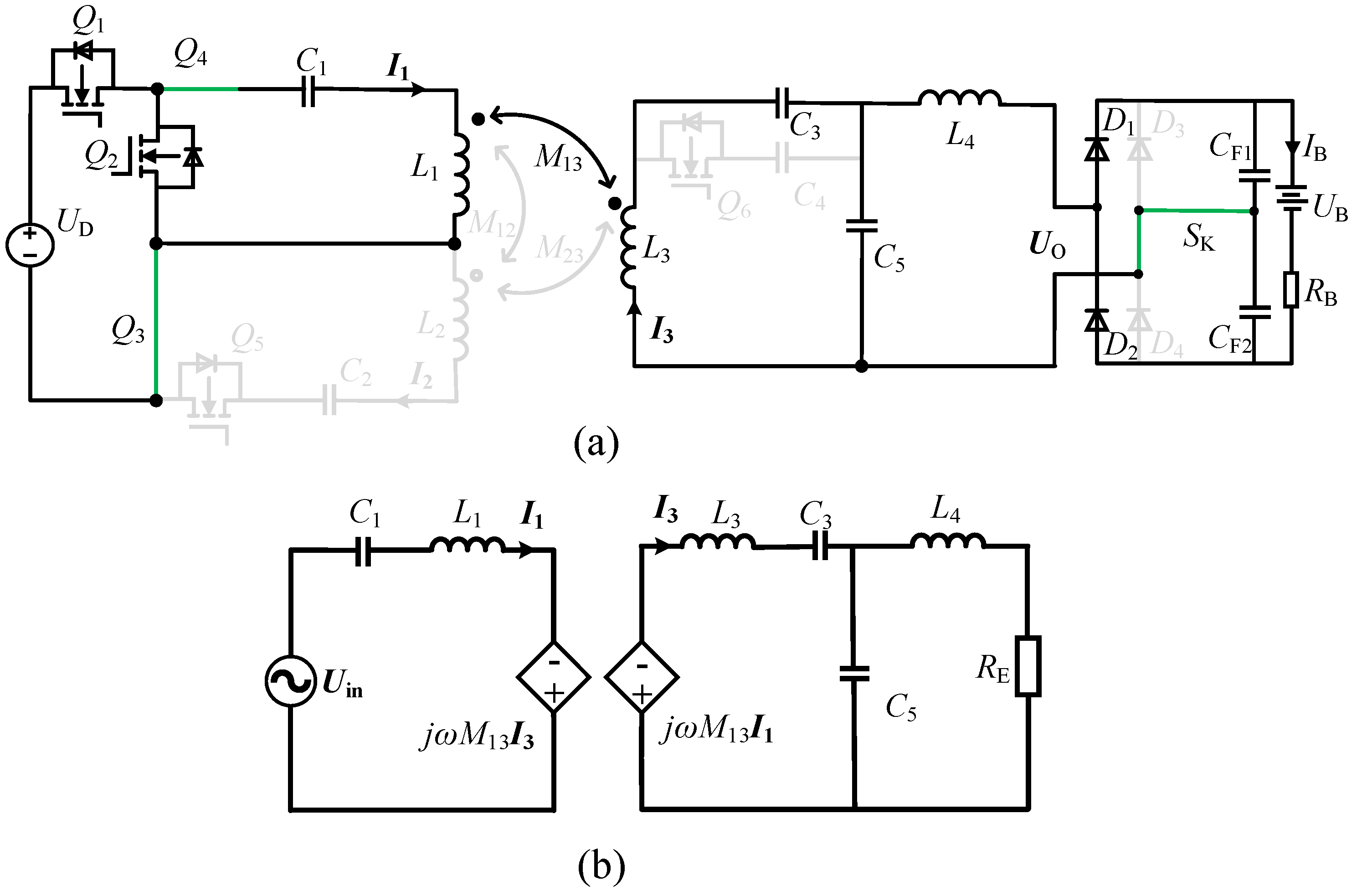
According to the control logic in Figure 2c, when the transmitter-side MOSFETs Q 1 and Q 2 operate alternately at a 50% duty cycle and Q 3 and Q 4 are on, Q 5 is off, only Loop 1 operate, and the equivalent inverter is suspended in Loop 1, acting as the transmitter circuit, while Loop 2 is cut off. When the receiving-side MOSFET Q 6 is turned off, only C 3 connected in circuit, matching the resonant conditions in CC1 mode. At this point, the LCC compensation structure formed by C 3 , C 5 , and L 4 , along with transmitting coil L 3 , acts as the receiving circuit. S K is turned on, reconstructing the rectifier into a voltage doubler rectifier. To simplify the analysis, the equivalent circuit of the first S- LCC two-coil structure configured in CV1 mode is given, as shown in Figure 5b. As evident from Figure 5b, using KVL can be used to obtain the equation is as follows.
U i n = j ω L 1 + 1 j ω C 1 I 1 j ω M 13 I 3 0 = j ω M 13 I 1 + j ω L 3 + 1 j ω C 3 + 1 j ω C S I 3 1 j ω C 5 I 4 0 = 1 j ω C 5 I 3 + j ω L 4 + 1 j ω C 5 + R E I 4
Substituting the resonant condition in Equation (1) and equation U in = 2 π U D for the half-bridge inverter into Equation (6), the first charging voltage U B 1 and input impedance Z i n in CV1 mode can be express as.
U B 1 = π 2 U O = L 4 U D M 13 Z in = U in I 1 = 2 M 13 2 R B π 2 L 4 2
As can be seen from (7), the first charging voltage U B 1 is independent of the variable battery load R B . Therefore, the system can achieve a CV output in CV1 mode. In addition, Z i n is purely resistive. In other words, the proposed system can achieve ZPA operation in CV1 mode.

2.4. CV2 Mode

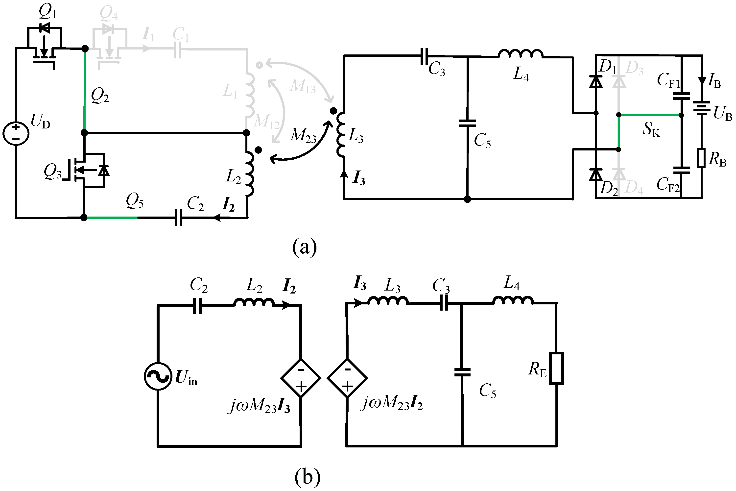
According to the control logic in Figure 2d, when the transmitter-side MOSFETs Q1 and Q3 operate alternately at a 50% duty cycle and Q 2 and Q 5 are on, Q 4 is off, only Loop 2 operate, and the equivalent inverter is suspended in Loop 2, acting as the transmitter circuit, while Loop 1 is cut off. Similar to CV1 mode, the LCC compensation structure formed by C 3 , C 5 , and L 4 , along with transmitting coil L 3 , acts as the receiving circuit. To simplify the analysis, the equivalent circuit of the second S- LCC two-coil structure configured in CV2 mode is given, as shown in Figure 6b. As evident from Figure 6b, using KVL can be used to obtain the equation is as follows.
U i n = j ω L 2 + 1 j ω C 2 I 2 j ω M 23 I 3 0 = j ω M 23 I 2 + j ω L 3 + 1 j ω C 3 + 1 j ω C S I 3 1 j ω C 5 I 4 0 = 1 j ω C 5 I 3 + j ω L 4 + 1 j ω C 5 + R E I 4
Substituting the resonant condition in Equation (1) and equation U in = 2 π U D for the half-bridge inverter into Equation (8), the second charging voltage U B 2 and input impedance Z i n in CV2 mode can be express as.
U B 2 = π 2 U O = L 4 U D M 23 Z in = U in I 1 = 2 M 23 2 R B π 2 L 4 2
As can be seen from (9), the second charging voltage U B 2 is independent of the variable battery load R B . Therefore, the system can achieve a CV output in CV2 mode. In addition, Z i n is purely resistive. In other words, the proposed system can achieve ZPA operation in CV2 mode.

3. Simulation Analysis

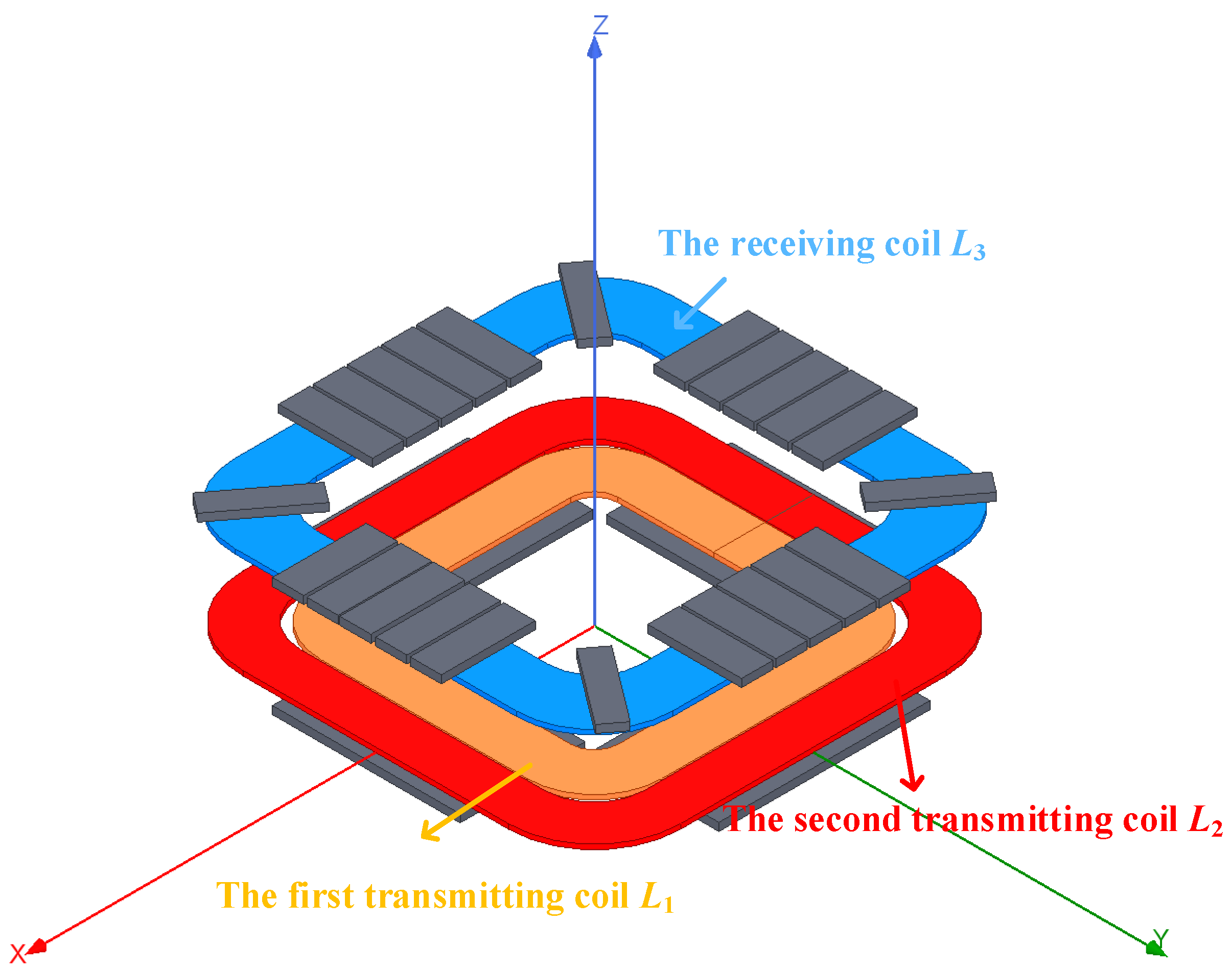
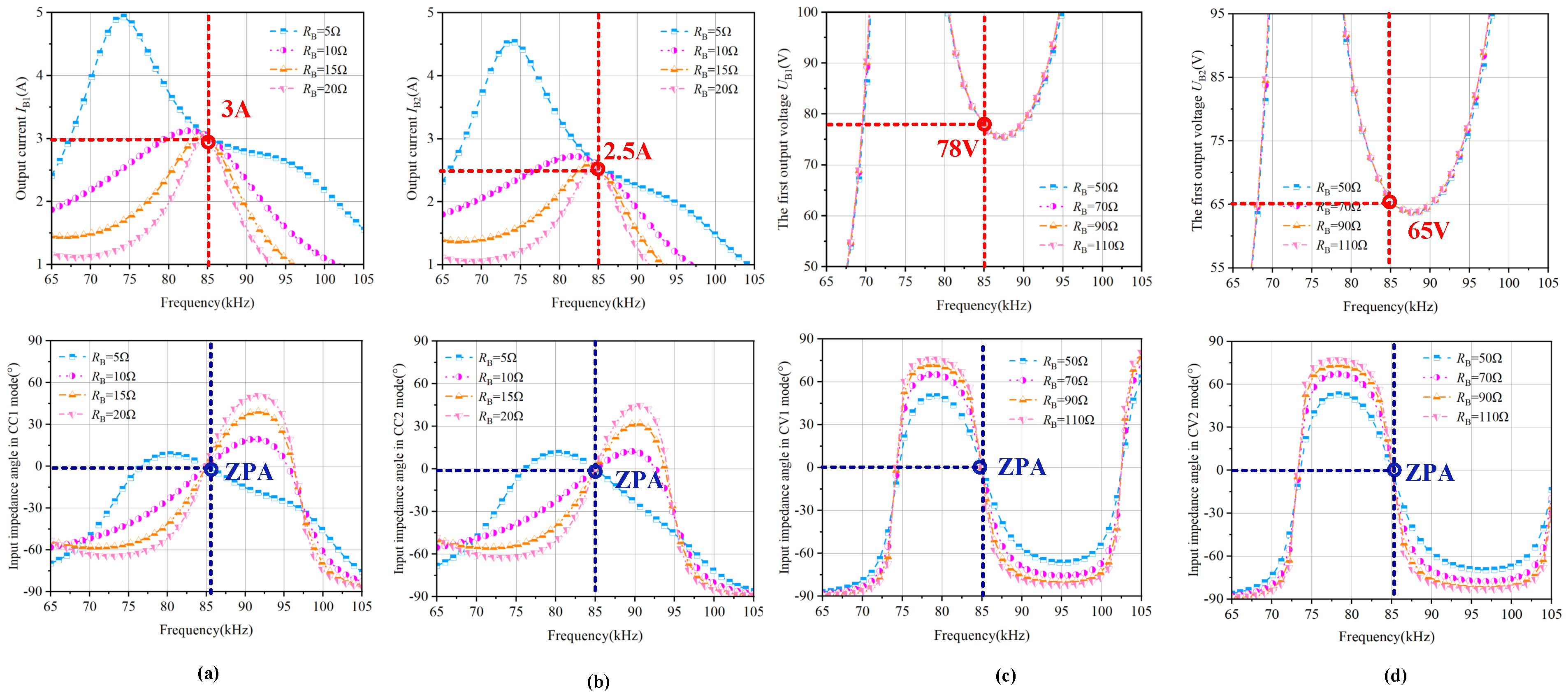
Based on a sound parameter design process, the designed magnetic coupler model is shown in Figure 7, and the detailed simulation parameters are listed in Table 1. The proposed WPT system can achieve two different constant current outputs of 3/2.5 A and two different constant voltage outputs of 78/65 V under the above parameter conditions.
In order to meet the need of further verifying the feasibility of the parameters, the output characteristic curves under different frequency conditions are given based on the parameters in Table 1, as shown in Figure 8. As evident from Figure 8a–d, under the frequency condition of 85 kHz, I B 1 , I B 2 , U B 1 and U B 2 can be maintained at 3 A, 2.5 A, 78 V and 65 V respectively. Besides, the input impedance angles of the above four modes are all zero under this condition. Therefore, the above results verify that the proposed system can achieve constant output characteristics under ZPA conditions.

4. Experimental Verification

4.1. Experimental Prototype and Experimental Parameters

To verify the feasibility of the system, an experimental prototype is built that can selectively operate at current specifications of 3 A/2.5 A and voltage specifications of 78 V/65 V according to charging requirements. Detailed experimental parameters are listed in Table 2.
Based on the experimental circuit parameters in Table 2, the absolute maximum current and voltage stresses across the MOSFETs and diodes can be calculated or simulated. Therefore, through appropriate hardware selection and considering a safety margin of 1.5–3 times, the MOSFETs selected for Q 4 , Q 5 , and Q 6 are IPP60R099CP (600 V/30 A), the MOSFETs for Q 1 , Q 2 , and Q 3 are IRFP250NPBF (200 V/30 A), and the MOSFET for S K is HSP30N15A (100 V/30 A). In addition, the diode is MBR30200F (200 V/30 A).

4.2. Experimental Waveforms

Figure 9 shows that under different load R B conditions, I B 1 , I B 2 , U B 1 and U B 2 can be maintained at 3 A, 2.5 A, 78 V, and 65 V, respectively. Furthermore, in CC1 and CV1 modes, U i n and I 1 are in phase, meaning the system can achieve ZPA operation in these modes. In CC2 and CV2 modes, U i n and I 2 are in phase, meaning the system can achieve ZPA operation in these modes.

4.3. Experimental Efficiency

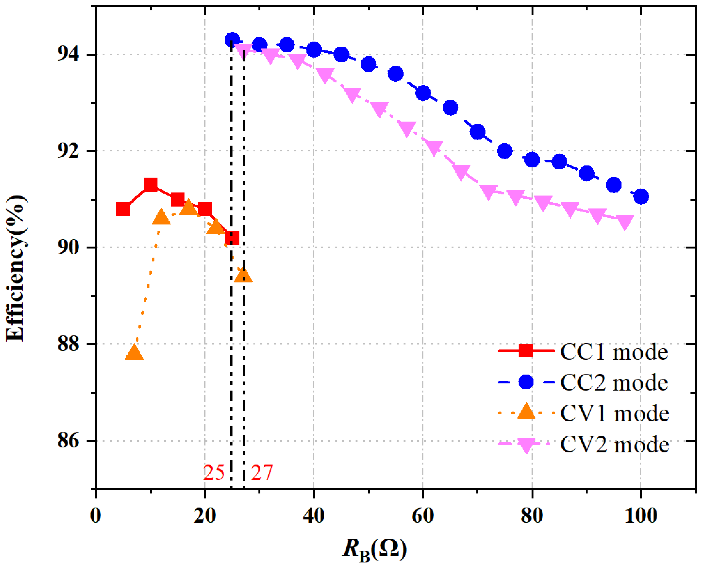
Figure 10 shows the efficiency curves for the four modes. As can be seen from Figure 10, the efficiency ranges from 90.1% to 91.3% in CC1 mode, 87.8% to 90.4% in CC2 mode, 91.1% to 94.3% in CV1 mode, and 90.3% to 94.1% in CV2 mode. Therefore, the overall efficiency of the proposed WPT system meets high standards during operation.

5. The Comprehensive Comparison Results

To further demonstrate the superior characteristics of the proposed system, the comprehensive comparison results of this work with previous related works are as follows:
(1) Compared with the three typical closed-loop control techniques proposed in refs. [17,18,19,20,21,22], the proposed system simplifies the design difficulty of the system controller and does not require additional DC-DC circuits beyond compensation components. Constant output can be achieved solely through the inherent structural characteristics of the system itself.
(2) Compared with the topology switching method and reconfigurable method used in refs. [23,24,28], the proposed system uses fewer AC switches and can achieve more functions. From a functional perspective, the system has obvious advantages. It is worth mentioning The proposed system is not limited by LCR parameters and has higher design freedom. Different output configurations can be achieved by configuring the series compensation inductor L 4 .
(3) Compared with the dual-frequency switching method adopted in refs. [25,26], the proposed system has only one fixed operating frequency, which avoids the problem of complex circuit parameter design and difficulty in limiting the operating frequency range in the dual-frequency switching method.
(4) Although the method in refs. [27] can be used to realize the power supply of electric bicycles of different specifications, each additional output specification requires an additional independent channel, a geometrically increased number of compensation components and AC switches, which poses a significant challenge to the system cost, weight and volume.
(5) The superior feature of the proposed system is that it can selectively operate in two different CC modes and two different CV modes, satisfying users’ daily needs for fast and slow charging while further enabling charging for two different specifications of electric bicycles. Functionally, this system is superior to the system proposed in refs. [17,18,19,20,21,22,23,24,25,26,27,28].

6. Conclusions

This paper proposes a multi-mode wireless charging system based on a reconfigurable transmitter. This system can charge batteries of different specifications and can automatically select between fast and slow charging modes based on actual needs. By applying different control logic to the reconfigurable inverter, the system can achieve four operating modes: two different CC modes and two different CV modes. Furthermore, this paper proposes a method of adding a voltage doubler rectifier on the receiving side to further improve the system’s efficiency under light load conditions. Based on the aforementioned theoretical analysis, a prototype system was designed and built to verify its performance. The results showed that the system can achieve a 3 A CC output in CC1 mode, a 2.2 A CC output in CC2 mode, a 78 V CV output in CV1 mode, and a 65 V CV output in CV2 mode.

Author Contributions

Conceptualization, D.D. and S.X.; methodology, D.D.; and Y.Z.; software, D.D.; validation, D.D., Y.Z. and X.C.; formal analysis, S.X.; investigation, D.D.; resources, Y.Z.; data curation, X.C.; writing—original draft preparation, D.D.; writing—review and editing, X.C.; visualization, Y.Z.; supervision, S.X.; project administration, D.D.; funding acquisition, D.D. All authors have read and agreed to the published version of the manuscript.

Funding

This research received no external funding.

Informed Consent Statement

Not applicable for studies not involving humans. You might also choose to exclude this statement if the study did not involve humans.

Data Availability Statement

Data are contained within the article.

Conflicts of Interest

The authors declare no conflicts of interest.

References

  1. Chen, Y.; Zhang, Z.; Yang, B.; Zhang, B.; Fu, L.; He, Z.; Mai, R. A Clamp Circuit-Based Inductive Power Transfer System with Re-configurable Rectifier Tolerating Extensive Coupling Variations. IEEE Trans. Power Electron. 2024, 39, 1942–1946. [Google Scholar] [CrossRef]
  2. Rong, E.; Sun, P.; Qiao, K.; Zhang, X.; Yang, G.; Wu, X. Six-plate and hybrid-dielectric capacitive coupler for underwater wireless power transfer. IEEE Trans. Power Electron. 2023, 39, 2867–2881. [Google Scholar] [CrossRef]
  3. Li, J.; Chen, F.; Zhu, R.; Chen, Y.; Mai, R. 3-D Embedded Receiving Coil Positioning Based on Decoupled Transformer for Wireless Sensor Power Supply System. IEEE Trans. Power Electron. 2025, 10, 14222–14227. [Google Scholar] [CrossRef]
  4. Liang, Z.; Zhu, L.; Sun, Y.; Li, J.; Qin, R.; Arka, B.; Costinett, D.; Bai, H. Full Integration of On-Board Charger, Auxiliary Power Module, and Wireless Charger for Electric Vehicles Using Multipurpose Magnetic Couplers. IEEE Trans. Ind. Electron. 2024, 71, 9962–9967. [Google Scholar] [CrossRef]
  5. Liu, X.; Gao, F.; Wang, W.H. A Series–Parallel Transformer-Based WPT System for 400-V and 800-V Electric Vehicles with Z1 or Z2 Class. IEEE Trans. Power Electron. 2024, 39, 1749–1761. [Google Scholar] [CrossRef]
  6. Li, G.; Ma, H. A Hybrid IPT System with High-Misalignment Tolerance and Inherent CC–CV Output Characteristics for EVs Charging Applications. IEEE J. Emerg. Sel. Top. Power Electron. 2022, 10, 3152–3160. [Google Scholar] [CrossRef]
  7. Li, M.; Khaleghi, A.; Hasanvand, A.; Narayanan, R.P.; Balasingham, I. A New Design and Analysis for Metasurface-Based Near-Field Magnetic Wireless Power Transfer for Deep Implants. IEEE Trans. Power Electron. 2024, 39, 6442–6454. [Google Scholar] [CrossRef]
  8. Mukherjee, D.; Rainu, S.K.; Singh, N.; Mallick, D.; Miniaturized, A. Low-Frequency Magnetoelectric Wireless Power Transfer System for Powering Biomedical Implants. IEEE Trans. Biomed. Circuits Syst. 2024, 18, 438–450. [Google Scholar] [CrossRef] [PubMed]
  9. Shah, I.A.; Zada, M.; Shah, S.A.; Basir, A.; Yoo, H. Flexible Metasurface-Coupled Efficient Wireless Power Transfer System for Implantable Devices. IEEE Trans. Microw. Theory Tech. 2024, 72, 2534–2547. [Google Scholar] [CrossRef]
  10. Yang, L.; Dong, K.; Wang, Y.; Cai, C. Analysis and Design of a Dual-Receiver WPT System with Constant Current and Constant Voltage Dual-Type Outputs. IEEE Trans. Transp. Electrif. 2025, 11, 4060–4069. [Google Scholar] [CrossRef]
  11. Mai, R.; Luo, Y.; Yang, B.; Song, Y.; Liu, S.; He, Z. Decoupling circuit for automated guided vehicles IPT charging systems with dual receivers. IEEE Trans. Power Electron. 2020, 35, 6652–6657. [Google Scholar] [CrossRef]
  12. Cai, C.; Wang, J.; Saeedifard, M.; Zhang, P.; Chen, R.; Zhang, J. Gyrator-Gain Variable WPT Topology for MC-Unconstrained CC Output Customization Using Simplified Capacitance Tuning. IEEE Trans. Ind. Electron. 2025, 71, 3594–3605. [Google Scholar] [CrossRef]
  13. Yang, L.; Wang, Y.; Guo, P.; Dong, K.; Cai, C. A Reconfigurable Rectifier Based Communication-Free Wireless LED Driver with Dual-Customization CC Outputs. IEEE Trans. Power Electron. 2025, 40, 2680–2684. [Google Scholar] [CrossRef]
  14. Wang, Q.; Li, Z.; Yang, B.; Lu, Y.; Mai, R.; He, Z.; Chen, Y. Inductive Power Transfer System with Constant Current-Constant Voltage Charging Tolerating Misalignment Based on Multiobjective Optimization for Compensation Topology. IEEE Trans. Power Electron. 2024, 40, 4581–4591. [Google Scholar] [CrossRef]
  15. Yang, L.; Xu, S.; Wang, Y.; Jiang, J.; Shi, Y.; Wang, M.; Cai, C. A Reconfigurable Magnetic Integrated Transmitter-Based Multimode WPT System for Electric Bicycle Charging. IEEE Trans. Transp. Electrif. 2025, 11, 11805–11815. [Google Scholar] [CrossRef]
  16. Xie, R.; Wu, Y.; Tang, H.; Zhuang, Y.; Zhang, Y. A Strongly Coupled Vehicle-to-Vehicle Wireless Charging System for Emergency Charging Purposes with Constant-Current and Constant-Voltage Charging Capabilities. IEEE Trans. Power Electron. 2024, 39, 3985–3989. [Google Scholar] [CrossRef]
  17. Colak, K.; Asa, E.; Bojarski, M.; Czarkowski, D.; Onar, O.C. A Novel Phase-Shift Control of Semibridgeless Active Rectifier for Wireless Power Transfer. IEEE Trans. Power Electron. 2015, 30, 6288–6297. [Google Scholar] [CrossRef]
  18. Song, K.; Li, Z.; Jiang, J.; Zhu, C. Constant current/voltage charging operation for series-series and series-parallel compensated wireless power transfer systems employing primary-side controller. IEEE Trans. Power Electron. 2018, 33, 8065–8080. [Google Scholar] [CrossRef]
  19. Liu, N.; Habetler, T.G. Design of a Universal Inductive Charger for Multiple Electric Vehicle Models. IEEE Trans. Power Electron. 2015, 30, 6378–6390. [Google Scholar] [CrossRef]
  20. Gati, E.; Kampitsis, G.; Manias, S. Variable Frequency Controller for Inductive Power Transfer in Dynamic Conditions. IEEE Trans. Power Electron. 2017, 32, 1684–1696. [Google Scholar] [CrossRef]
  21. Huang, Z.; Wong, S.; Tse, C. Comparison of Basic Inductive Power Transfer Systems with Linear Control Achieving Optimized Efffciency. IEEE Trans. Power Electron. 2020, 35, 3276–3286. [Google Scholar] [CrossRef]
  22. Li, Z.; Zhu, C.; Jiang, J.; Song, K.; Chan, K.; Wei, G. A 3-kW wireless power transfer system for sightseeing car supercapacitor charge. IEEE Trans. Power Electron. 2017, 32, 3301–3316. [Google Scholar] [CrossRef]
  23. Qu, X.; Han, H.; Wong, S. Hybrid IPT topologies with constant current or constant voltage output for battery charging applications. IEEE Trans. Power Electron. 2015, 30, 6329–6337. [Google Scholar] [CrossRef]
  24. Li, Y.; Hu, J.; Liu, M.; Chen, Y.; Chan, K.; He, Z.; Mai, R. Reconfigurable Intermediate Resonant Circuit Based WPT System with Load-Independent Constant Output Current and Voltage for Charging Battery. IEEE Trans. Power Electron. 2019, 34, 1988–1992. [Google Scholar] [CrossRef]
  25. Mai, R.; Li, Q.; Chen, Y.; Yang, B.; He, Z. Variable parameter and variable frequency-based IPT charging system with configurable charge current and charge voltage. IET Power Electron. 2020, 13, 751–757. [Google Scholar] [CrossRef]
  26. Vu, V.-B.; Tran, D.-H.; Choi, W. Implementation of the constant current and constant voltage charge of inductive power transfer systems with the double-sided LCC compensation topology for electric vehicle battery charge applications. IEEE Trans Power Electron. 2018, 33, 7398–7410. [Google Scholar] [CrossRef]
  27. Chen, Y.; Kou, Z.; Zhang, Y.; He, Z.; Mai, R.; Cao, G. Hybrid Topology with Configurable Charge Current and Charge Voltage Output-Based WPT Charger for Massive Electric Bicycles. IEEE J. Emerg. Sel. Top. Power Electron. 2018, 6, 1581–1594. [Google Scholar] [CrossRef]
  28. Yang, L.; Shao, S.; Zhou, X. A Three-Coil IPT Charger with CC and CV Outputs Through Circuit Reconfiguration. IEEE Trans. Circuits Syst. II Express Briefs 2024, 71, 3558–3562. [Google Scholar] [CrossRef]
Figure 1. The overall architecture of the proposed dual-mode WPT system.
Electronics 14 04315 g001
Figure 2. The corresponding control logic. (a) CC1 mode. (b) CC2 mode. (c) CV1 mode. (d) CV2 mode.
Electronics 14 04315 g002
Figure 3. The overall architecture of the proposed system in CC1 Mode. (a) The circuit topology. (b) The equivalent circuit.
Electronics 14 04315 g003
Figure 4. The overall architecture of the proposed system in CC2 Mode. (a) The circuit topology. (b) The equivalent circuit.
Electronics 14 04315 g004
Figure 5. The overall architecture of the proposed system in CV1 Mode. (a) The circuit topology. (b) The equivalent circuit.
Electronics 14 04315 g005
Figure 6. The overall architecture of the proposed system in CV2 Mode. (a) The circuit topology. (b) The equivalent circuit.
Electronics 14 04315 g006
Figure 7. The designed magnetic coupler model.
Electronics 14 04315 g007
Figure 8. Output characteristic curves at different frequencies. (a) Output current and input impedance angle in CC1 mode; (b) Output current and input impedance angle in CC2 mode; (c) Output voltage and input impedance angle in CV1 mode; (d) Output voltage and input impedance angle in CV2 mode.
Electronics 14 04315 g008
Figure 9. Experimental waveforms. (a) CC1 mode; (b) CC2 mode; (c) CV1 mode; (d) CV2 mode.
Electronics 14 04315 g009
Figure 10. Experimental efficiency.
Electronics 14 04315 g010
Table 1. The detailed simulation parameters of the system.
ParametersValueParametersValueParametersValue
f85 kHz U D 100 V I B 1 3 A
I B 2 2.5 A U B 1 78 V U B 2 65 V
L 1 66.2 μ H L 2 73.8 μ H L 3 102.85 μ H
L 4 20 μ H C 1 52.96 n F C 2 47.51 n F
C 3 42.32 n F C 4 41.88 n F C 5 175.3 n F
M 12 38 μ H M 13 25.8 μ H M 23 30.35 μ H
Table 2. The detailed experimental parameters of the system.
ParametersValueParametersValueParametersValue
f85 kHz U D 100 V I B 1 3 A
I B 2 2.5 A U B 1 78 V U B 2 65 V
L 1 67.1 μ H L 2 73.92 μ H L 3 102.65 μ H
L 4 20.3 μ H C 1 51.96 n F C 2 47.71 n F
C 3 41.82 n F C 4 41.38 n F C 5 175.72 n F
M 12 38.23 μ H M 13 25.98 μ H M 23 30.15 μ H
Disclaimer/Publisher’s Note: The statements, opinions and data contained in all publications are solely those of the individual author(s) and contributor(s) and not of MDPI and/or the editor(s). MDPI and/or the editor(s) disclaim responsibility for any injury to people or property resulting from any ideas, methods, instructions or products referred to in the content.