Article

Electric-Field and Magnetic-Field Decoupled Wireless Power and Full-Duplex Signal Transfer Technology for Pre-Embedded Sensors

Lanzhou Power Supply Company, State Grid Gansu Electric Power Company, Lanzhou 730030, China
*
Author to whom correspondence should be addressed.
Electronics 2025, 14(21), 4302; https://doi.org/10.3390/electronics14214302
Submission received: 17 October 2025 / Revised: 29 October 2025 / Accepted: 29 October 2025 / Published: 31 October 2025

Abstract

Pre-embedded sensors for concrete structure monitoring face bottlenecks in power supply and data transmission. Existing power supply solutions such as photovoltaic systems and batteries suffer from drawbacks including energy randomness and structural damage to concrete caused by their installation methods. Additionally, commercial wireless communication signals exhibit issues like strong attenuation and poor security during propagation. This paper proposes a hybrid electromagnetic field decoupled parallel transmission technology for power and signals. It utilizes the inherent decoupling characteristic of electric and magnetic fields within the near-field range to construct independent power/signal transfer channels, and achieves independent full-duplex transmission of uplink/downlink data via orthogonal coupling plates. Mathematical models for the power and signal channels are established, and finite element simulations are conducted. A parameter design method for the power compensation network and signal filtering circuit is also proposed. An experimental setup is built, with a coupler outer dimension of 200 mm × 200 mm, a coupling distance of 10 mm, and a thickness of 16 mm for both the transmitting and receiving sides. Experimental results show that the system achieves power transmission with a power of 100 W and an efficiency of 82%, while simultaneously realizing full-duplex communication with a bidirectional rate of 9600 bit/s. Moreover, no bit errors occur within 300,000 characters of bidirectional data.

1. Introduction

With the intelligent development of infrastructure, there is an increasing demand for safety monitoring of concrete structures [1]. As core sensing components, concrete sensors realize real-time monitoring of structural states through integrated sensing technology, and are widely used in fields such as health monitoring of intelligent buildings and long-term performance evaluation of bridges and tunnels [2,3,4]. Currently, sensor technology has formed a diversified system, including types such as fiber Bragg grating (FBG), vibrating wire, and ground nail [5,6]. Based on different principles, these sensors have their own advantages in monitoring accuracy, durability, and applicability, providing technical support for the full-life-cycle monitoring of concrete structures.
However, the continuous and reliable operation of sensors is highly dependent on power supply technologies, and existing methods such as photovoltaic (PV) power supply [7], energy storage batteries [8], and self-powered technologies [9] all have significant limitations. PV power supply is restricted by environmental lighting conditions, exhibiting significantly reduced efficiency in scenarios such as underground structures and bridge shadow areas. Energy storage batteries require regular replacement or charging, leading to high maintenance costs and a high risk of data interruption in remote engineering projects or long-term monitoring applications. Additionally, battery replacement necessitates grooving or drilling holes on the surface of concrete structures and reserving interfaces, which adversely affects the structural integrity of concrete. Self-powered technologies based on vibration and temperature difference possess the advantage of being passive. Their energy harvesting efficiency is low, making it difficult to support the long-term continuous operation of high-precision, multi-node sensors. These issues limit the stability and applicability of monitoring systems, becoming a key bottleneck restricting the promotion of intelligent monitoring technologies for concrete structures.
Wireless power transfer (WPT) technology, a non-contact power supply solution, breaks through the limitations of wired power supply based on the principle of electromagnetic induction [10,11,12]. In concrete structure monitoring, it possesses advantages including no structural damage, no exposed metal, adaptability to harsh environments, and support for long-term maintenance-free operation. It has been studied in scenarios such as pre-embedded concrete sensors [13,14], torque sensors for rotating equipment [15], and online sensors for high-voltage transmission lines [16]. This technology has become an important new path to address the power supply bottleneck in scenarios where wired power supply is inconvenient.
In addition, concrete sensors also have a demand for wireless bidirectional data transmission: on the one hand, transmitting the monitoring data from internal concrete sensors back to the outside; on the other hand, configuring the parameters of internal sensors from the outside. This demand faces dual challenges: the strong attenuation of commercial communication signals such as WLAN, 5G, and Bluetooth by the concrete medium leads to reduced transmission reliability, and the characteristic of open frequency bands being prone to interception poses a threat to data security. Compared with these technologies, near-field communication, relying on centimeter-level short-distance transmission and an electromagnetic coupling point-to-point communication mechanism, can significantly reduce the risk of signal leakage and improve privacy and anti-interference capability, making it particularly suitable for scenarios with strict data security requirements such as intelligent buildings and bridge health monitoring. Therefore, integrating wireless power transfer and near-field communication technologies to realize wireless parallel transmission of power and signals holds practical engineering significance for improving the reliability and security of intelligent monitoring systems for concrete structures.
At present, wireless power and signal transfer technology has mainly formed three typical technical schemes [17], namely the power modulation type, independent channel type, and shared channel type, and their technical characteristics and engineering applicability show significant differences.
The power modulation-based scheme achieves signal loading by directly modulating parameters such as the amplitude, frequency, or phase of the power transfer waveform. For instance, it changes the voltage amplitude by switching the parameters of main circuit components to correspond to binary signals. This scheme does not require complex hardware modules and features a simple circuit structure, and it was initially applied in consumer electronic devices (e.g., data feedback for the Qi standard for wireless charging of mobile phones) [18]. However, its signal transmission rate is limited by the power resonant frequency, making it suitable only for low-speed communication scenarios.
The shared channel-based scheme utilizes the same physical coupling channel to achieve frequency division multiplexing (FDM) or time division multiplexing (TDM) transmission of power and signals. For example, it enables power and signals to operate in different frequency bands through a dual resonant network [19]. This scheme possesses the advantages of both flexibility and integration, and suppresses cross talk through network impedance isolation or frequency-domain impedance characteristics. However, the core challenge of this technology lies in the extremely severe cross talk caused by power transmission to the signal channel, which requires processing via high-performance filtering and amplification circuits to achieve effective signal demodulation.
The independent channel-based scheme employs signal transmission links completely independent of the power channel [20]. This type of system typically establishes dedicated signal channels by adding additional coupling coils, with typical coil structures including the DDQ decoupled coil structure [21,22]. This scheme achieves decoupled transmission of power and signals through physical isolation, enabling high-speed data interaction for WPT systems. However, the dual-channel coupler undoubtedly increases the system volume and cost, which is unfavorable for applications in compact scenarios and those requiring mass installation.
Traditional independent channel-based schemes face bottlenecks in miniaturized applications. To address this issue, this paper proposes wireless power and full-duplex signal transfer technology based on an electric-field and magnetic-field decoupled principle. This technology achieves independent transmission of power and signals by leveraging the inherent decoupling property of magnetic and electric fields within the near-field range. Additionally, to meet the requirement of full-duplex signal transmission, this paper proposes an orthogonal electric-field decoupling mechanism to realize decoupled transmission of uplink and downlink data. The remainder of this paper is arranged as follows: Section 2 proposes a wireless power and signal transmission coupler based on electric- and magnetic-field decoupling; Section 3 describes mathematical modeling and design for the power channel and signal channel; Section 4 details experimental studies to verify the correctness of the proposed system and design method; and Section 5 concludes this paper.

2. Design of Hybrid Electric–Magnetic Field Coupler

Figure 1 shows the structure of the proposed electric-field and magnetic-field decoupled wireless power and full-duplex signal transfer system. The system comprises a WPT system and a duplex signal transfer system. The WPT system includes a transmitter circuit (Power Tx) with a full-bridge inverter, an LCC compensation circuit, and a transmitter coil, a receiver circuit (Power Rx) with a series compensation circuit, a power rectifier, and a load resistor. The signal transfer system consists of symmetric signal chains equipped with functional modules, including sine wave generation (①), first-stage amplification (②), ASK modulation (③), second-stage amplification (④), filter and amplification (⑤), envelope detection (⑥), envelope shaping (⑦), and ASK demodulation (⑧). The signal transfer system is separated by a capacitive coupler, which consists of eight metal plates, and a coupling capacitor exists between each pair of plates. These coupling capacitors not only connect the two sides of the signal transfer system but also may introduce cross talk between uplink and downlink data.

2.1. Coupler Structure Description

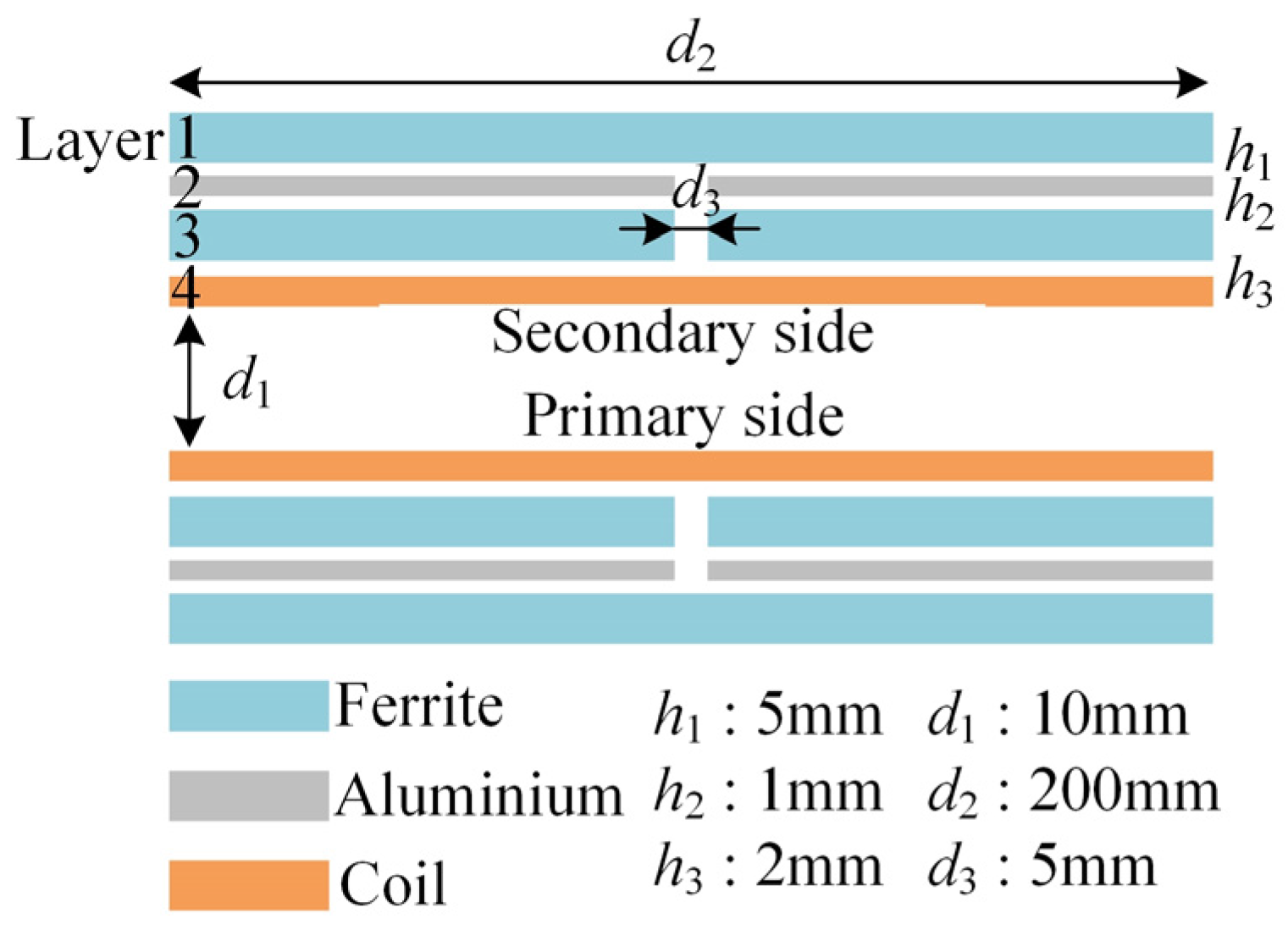
The side view of the system’s coupler is shown in Figure 2. The coupler is composed of ferrite, aluminum plates, and coils. The thickness of the ferrite in the first and third layers is h1 = 5 mm, the thickness of the aluminum plate in the second layer is h2 = 1 mm, and the thickness of the coil in the fourth layer is h3 = 2 mm. The air gap between the coils is d1 = 10 mm, the width of the coupler is d2 = 200 mm, and the distance between the aluminum plate and the third layer of ferrite is d3 = 5 mm. The primary and secondary sides of the coupler have the same structure. According to the laminated structure shown in Figure 2, the top view of the coupler can be divided into four layers from top to bottom, with an air gap of 2 mm between each layer. The top views and dimensions of each layer of the coupler are shown in Figure 3a–d.
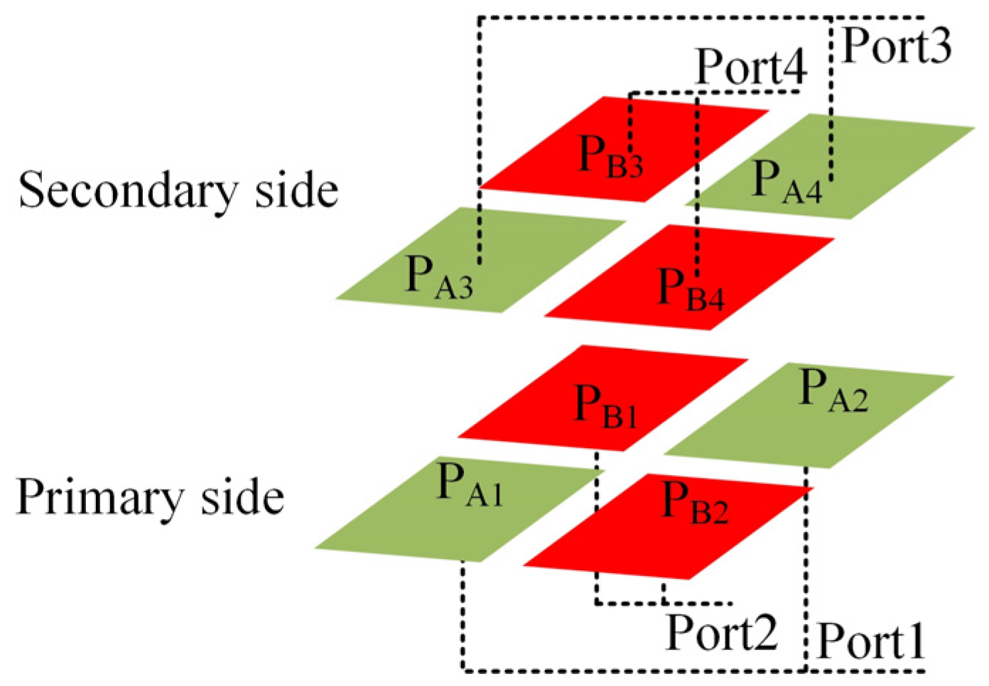
There is one inductive coil on both the primary side and the secondary side of the coupler, adopting a single-transmitter and single-receiver configuration for power transmission. There are four plates on each of the primary and secondary sides, and two plates form one port, thus realizing a dual-transmitter and dual-receiver setup for signal transmission. From the perspective of the capacitive coupler, the composition of its transmitting and receiving ports is as shown in Figure 4. Specifically, Port 1 sends data from the primary side to the secondary side, which is received by Port 3 on the secondary side, and Port 4 sends data from the secondary side to the primary side, which is received by Port 2 on the primary side.

2.2. Finite Element Simulation of Coupler

In the near-field range, the magnetic field and electric field are decoupled, so transmissions between the inductive coupler and the capacitive coupler do not interfere with each other. The coupler designed in this paper transmits magnetic-field energy through coils (which is further used for power transmission) and electric-field energy through plates (which is further used for signal transmission). This paper will verify the decoupling between coils and plates and the decoupling between ports in the capacitive coupler through finite element simulation.
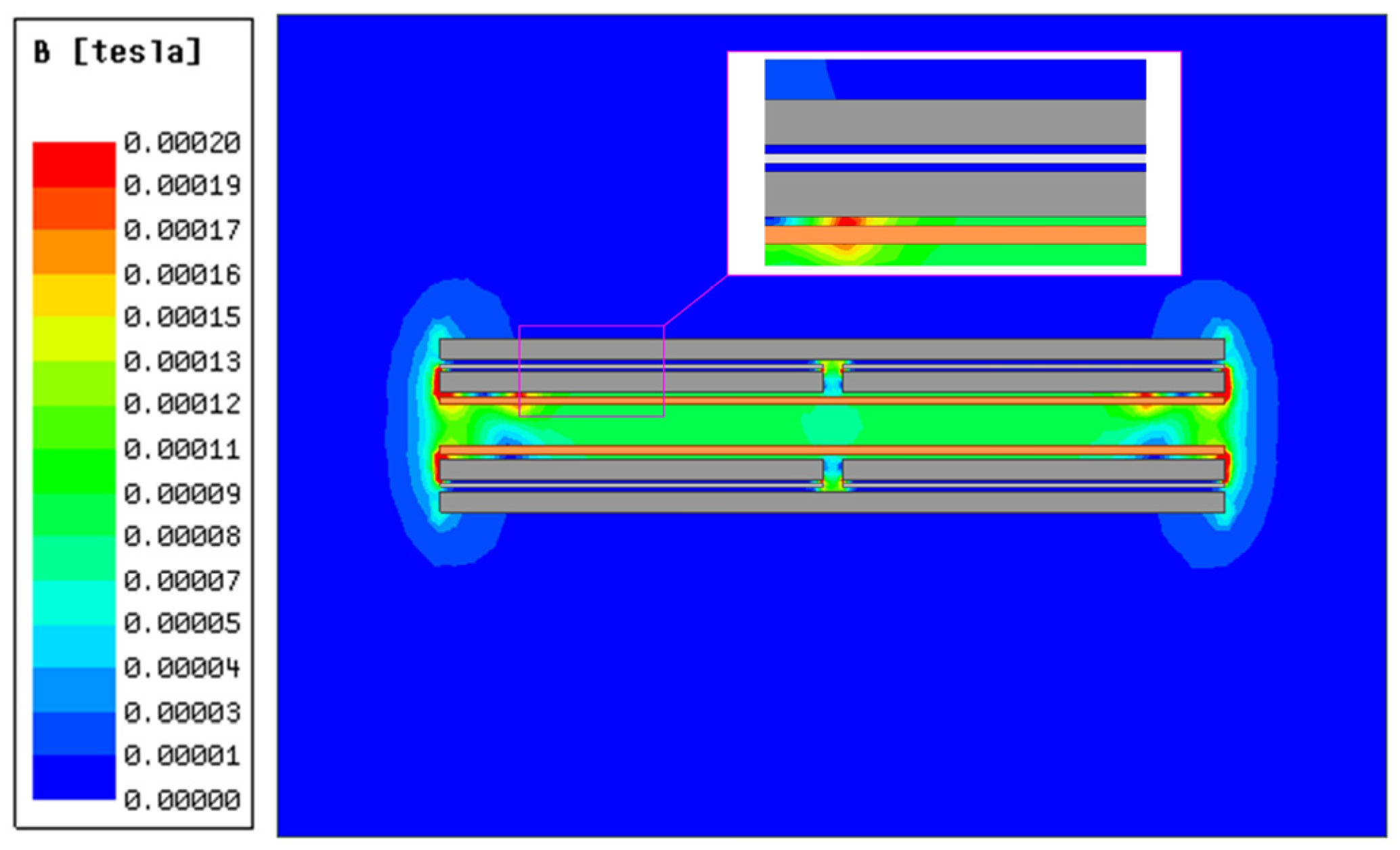
First, the decoupling between coils and plates is verified. A coupler simulation model is built, and current excitation is applied to the coils. The obtained magnetic-field cloud diagram of the coupler is shown in Figure 5. It can be seen in Figure 5 that the magnetic-field intensity near the aluminum plate is much smaller than that in spaces such as the coupling air gap, and the magnetic field will not produce a significant eddy current effect on the aluminum plate.
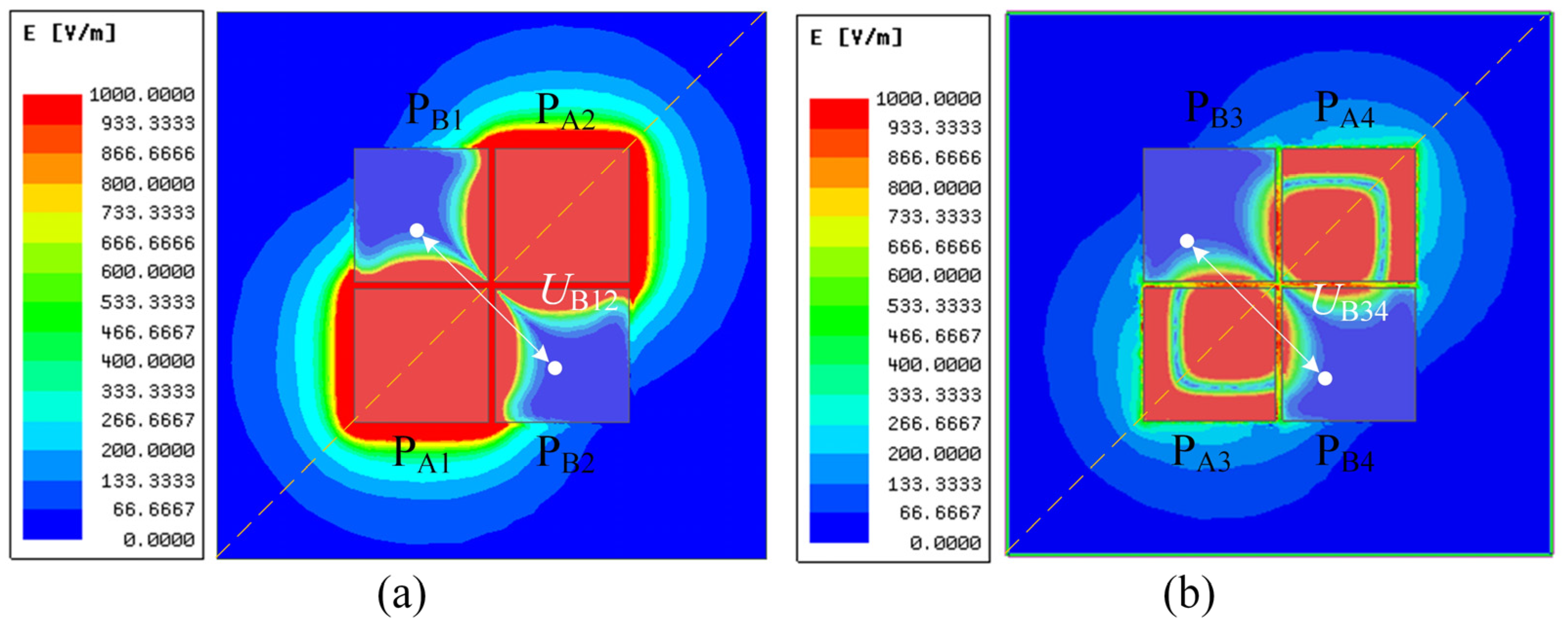
All plates in Figure 6 have the same size and adopt a symmetric layout. When excitation is applied to Port 1 (PA1 and PA2), plates PB1, PB2, PB3, and PB4 can form an equipotential body. In the simulation, an excitation voltage is first applied to Port 1, and then the decoupling principle of the coupler is analyzed by observing the electric field distribution characteristics around Ports 2, 3, and 4.
Figure 6a shows an electric-field cloud diagram near the four plates on the primary side (PA1, PA2, PB1, and PB2), and Figure 6b presents the corresponding electric-field distribution near the four plates on the secondary side (PA3, PA4, PB3, and PB4). For any two points on plates PB1 and PB2 that are symmetric about the diagonal line, their potentials are exactly equal. This indicates that the induced voltage U12 generated on plates PB1 and PB2 by the excitation of plates PA1 and PA2 is zero. From the perspective of the overall characteristics of the plates, PB1 and PB2 are equipotential bodies, which proves that decoupling is achieved between Port 1 and Port 2.
Similarly, it can be seen from the results shown in Figure 6b that plates PB3 and PB4 are also symmetric about the diagonal plane. Therefore, the potentials of any symmetric points on plates PB3 and PB4 remain consistent. Analyzed from the overall perspective of the plates, PB3 and PB4 are equipotential bodies, indicating that the induced voltage formed by the excitation of Port 1 on plates PB3 and PB4 is zero, thereby verifying the decoupling characteristics between Port 1 and Port 4.
Further analysis shows that due to the structural symmetry of the coupler, decoupling is also achieved between Port 2 and Port 1, as well as between Port 2 and Port 3. In summary, the eight-plate coupler structure proposed in this paper can effectively eliminate same-side coupling (Cm12, Cm34) and cross-coupling (Cm14, Cm23), realize decoupling between the two signal transmission channels, and ensure no cross talk in the bidirectional signal transmission.

3. System Modeling and Design

After adopting the proposed hybrid electric- and magnetic-field coupler, the power transmission channel, uplink data transmission channel, and downlink data transmission channel have been decoupled from each other. To achieve stable power transmission and reliable signal transmission, it is necessary to separately model and design the compensation network of the power transmission channel and the filter circuit of the signal transmission channel.

3.1. Power Transmission Channel

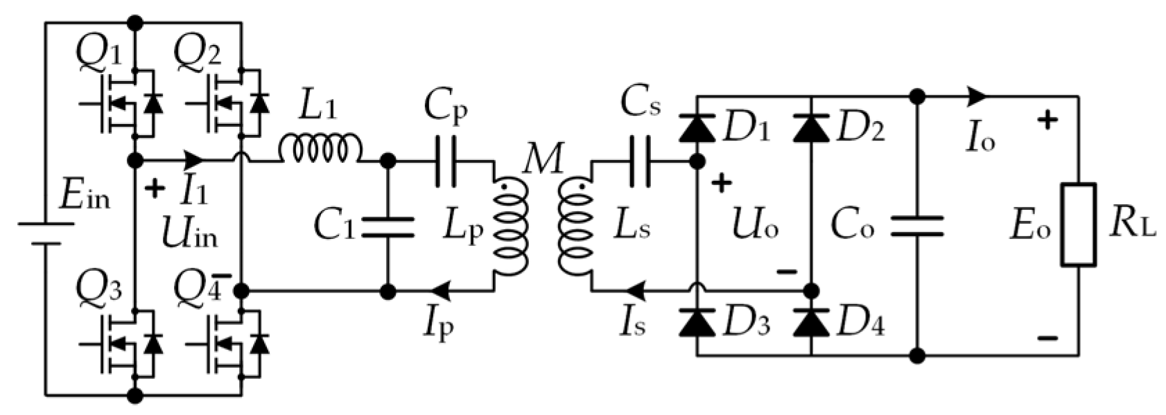
In the WPT system, the inductance of the coupling coils leads to an increase in reactive power in the circuit, thus reducing the power transmission efficiency of the system. The LCC-S resonant compensation network can not only reduce reactive power and improve transmission efficiency but also set the system voltage gain and achieve constant voltage output of the system by designing the parameters of the compensation circuit, which meets the requirements of the system design. The circuit of the LCC-S-based WPT system is shown in Figure 7.
In Figure 7, Ein is the DC input voltage; switches Q1–Q4 constitute the high-frequency inverter on the transmitting side, where Uin and I1 are the voltage and current output by the inverter, respectively; L1, C1, and Cp form the LCC compensation network on the transmitting side; Lp and Ls are the self-inductances of the coils on the transmitting side and receiving side; respectively; M is the mutual inductance between the transmitting coil and the receiving coil; Cs is the compensation capacitor on the receiving side; diodes D1–D4 and filter capacitor Co form the rectifier circuit on the receiving side, where Uo and Is are the voltage and current input to the rectifier circuit, respectively; RL is the equivalent load; and Eo and Io are the DC voltage and current of the load, respectively. The relationships between Eo and Uo and between Ein and Uin are as follows:
E o = π U o 2 2 U in = π E in 2 2
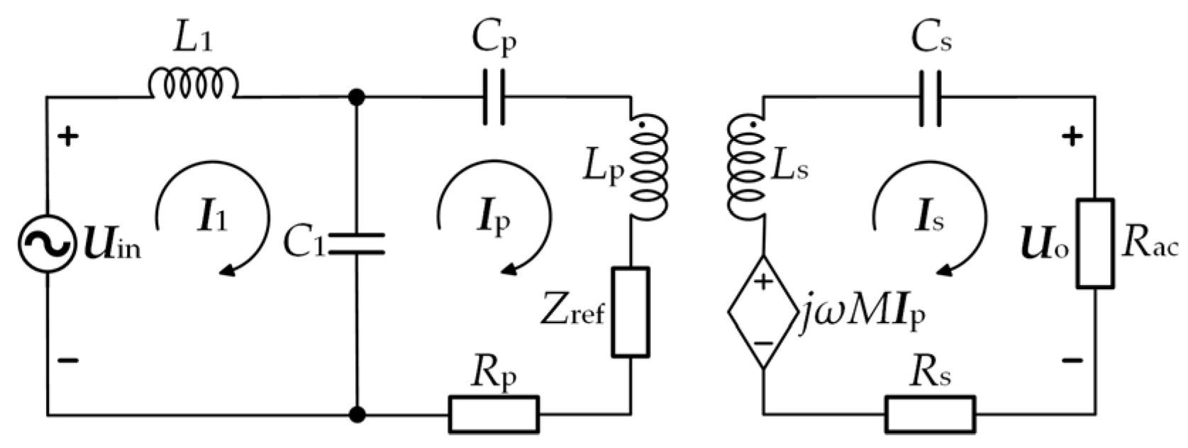
To analyze the resonant conditions of the LCC-S compensation network, an equivalent model based on the reflected impedance and mutual inductance theory is established in Figure 8.
In Figure 8, RP and Rs are the internal resistance of the transmitting side coil and the receiving side coil, respectively, while the internal resistance of the compensation inductor is much smaller than that of the coupling coils and thus is negligible. Ip is the current flowing through the transmitting coil. Rac is the equivalent AC impedance of the input port of the rectifier circuit. Assuming that the angular frequency of the system is ω, the resonant conditions of the system can be determined as follows:
j ω L 1 + 1 j ω C 1 = 0 1 j ω C 1 + 1 j ω C p + j ω L p = 0 j ω L s + 1 j ω C s = 0
The Kirchhoff voltage law (KVL) equation at the receiving side is:
j ω M I p + ( j ω L s + 1 j ω C s + R ac + R s ) I s = 0
The total impedance Zs at the receiving side is:
Z s = j ω L s + 1 j ω C s + R s + R ac
By combining Equations (2)–(4), the reflected impedance Zref from the receiving side to the transmitting side is obtained as:
Z ref = j ω M I s I p = ω 2 M 2 Z s = ω 2 M 2 R ac + R s
According to KVLs and Kirchhoff’s current laws (KCLs), the loop equations of the system can be written in matrix form as:
U in 0 U o = j ω L 1 + 1 j ω C 1 1 j ω C 1 0 1 j ω C 1 1 j ω C 1 + 1 j ω C p + j ω L p + Z ref + R p 0 0 j ω M ( j ω L s + 1 j ω C s + R s ) I 1 I p I s
By combining Equations (2)–(5), the current of each branch can be obtained as:
I 1 = U in ω 2 M 2 + R p ( R ac + R s ) ω 2 L 1 2 ( R ac + R s ) I p = U in ω L 1 I s = M U in L 1 ( R ac + R s )
The value of the equivalent load resistance Rac is:
R ac = 8 π 2 R L
Combining with Equation (7), the output voltage Uo of the system is obtained as:
U o = I s R ac = M U in R ac L 1 ( R ac + R s )
From the above derivation, the expression for the system voltage gain Gv is obtained as:
G v = U o U in = M R ac L 1 ( R ac + R s ) M L 1
It can be seen from Equations (7) and (10) that when the system internal resistance is ignored, the output voltage of the system is only related to the mutual inductance M and the primary series resonant inductor L1. After the design of the coupler is determined, both M and L1 are constant values, and the input voltage Uin of the system is also a given value. The output voltage of the system is constant, and the current flowing through the transmitting coil is also constant, that is, the system has a constant voltage output characteristic.
From Equation (7), the expressions for the input power Pin and output power Po of the system under the resonant state are obtained as follows:
P in = I s 2 R ac = M U in 2 R ac L 1 2 ( R ac + R s ) 2 P o = I s 2 R ac = U in 2 ω 2 M 2 + R p ( R ac + R s ) ω 2 L 1 2 ( R ac + R s )
It can be seen from Equation (11) that the system efficiency η is:
η = P o P i n = ω 2 M 2 R ac ( R ac + R s ) ω 2 M 2 + R p ( R ac + R s )
It can also be seen from Equation (11) that the output power of the system is affected by the series resonant inductor L1 on the transmitting side, mutual inductance M, and load resistance Rac. During circuit design, the appropriate compensation inductance value can be selected according to the rated output power.

3.2. Signal Transmission Channel

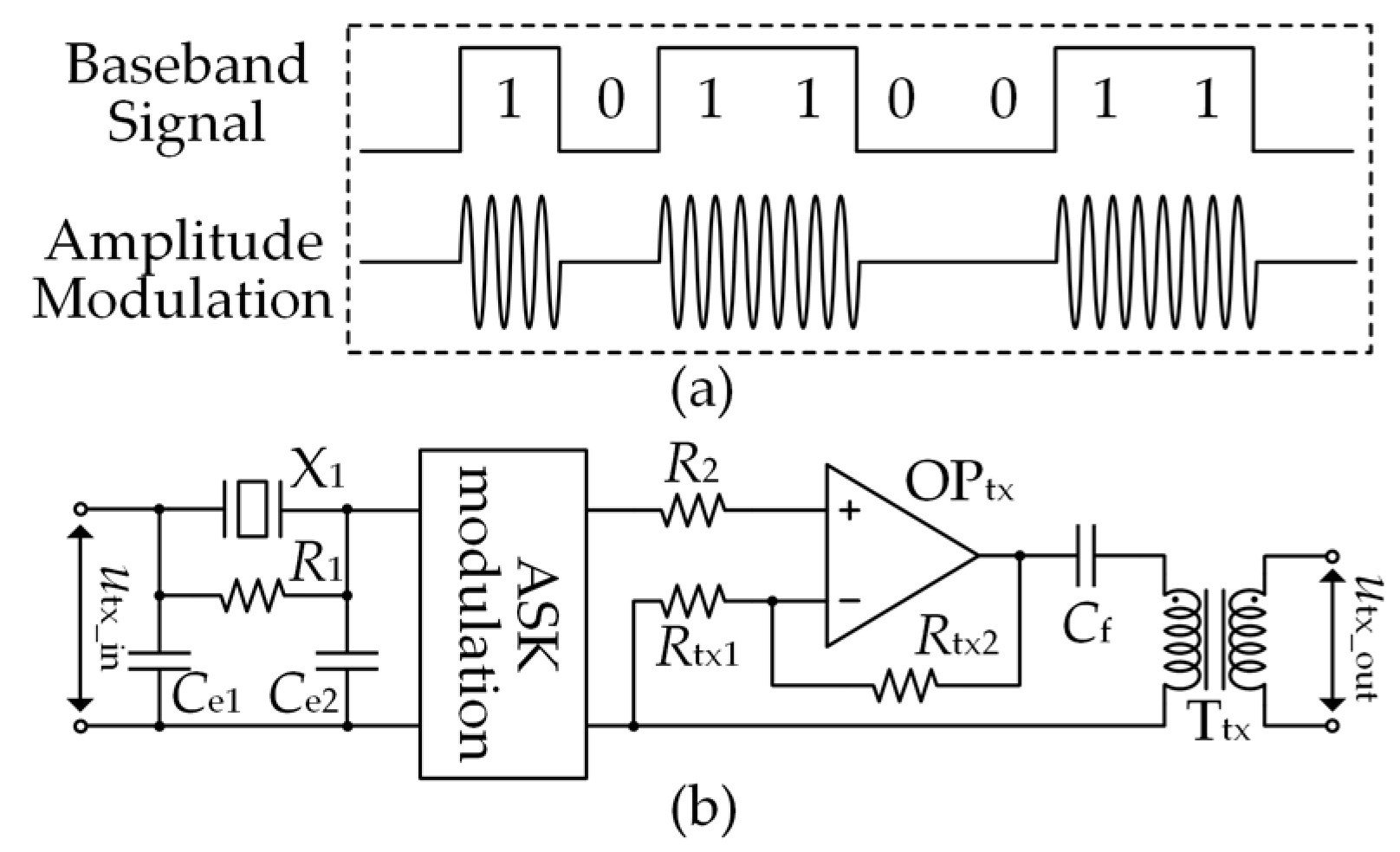
In the system, both bidirectional signal transmission systems employ amplitude shift keying (ASK) modulation-based signal circuits as the transmitters of the communication modules, and their modulation logic is as shown in Figure 9a. The main reasons are as follows. (1) ASK modulation offers advantages of simple implementation, low hardware cost, and low power consumption. It requires no complex algorithms or circuits, which fits the short-range, low-rate communication needs of the system. (2) Theoretical analyses show that the 1 cm-thick concrete causes minimal attenuation to the 8 MHz ASK signal of the system: only 0.061 dB (≈0.7%) in dry concrete and 0.151 dB (≈1.7%) in wet concrete. Additionally, the amplifying circuit at the receiver can further suppress attenuation, ensuring no impact of the concrete medium on normal signal transmission.
As shown in Figure 9b, the entire modulation circuit mainly consists of five parts, namely the oscillation circuit, ASK modulation circuit, amplification circuit, filtering circuit, and isolation circuit. utx_in is the input signal voltage of the transmitting side, and utx_out is the output signal voltage of the transmitting side. Rtx1 and Rtx2 are resistors in the transmitting-side amplification circuit. In the oscillation circuit, to ensure the normal oscillation of the crystal oscillator, the external load capacitors Ce1 and Ce2 should satisfy the following relationship:
C e 1 = C e 2 = 2 C L C t + C i
where CL is the internal capacitive load of the crystal oscillator, Ct is the PCB trace capacitance, and Ci is the parasitic capacitance of the chip pins. To reduce the Q-value of the crystal oscillator, suppress electromagnetic interference (EMI), and provide a DC operating point, a large resistor R1 is connected in parallel at both ends of the crystal oscillator.
The signal amplification circuit is used to amplify the modulated signal proportionally, which is conducive to the stable transmission of the signal. For the entire signal transmission circuit, the system gain Gtx of the signal transmitting side is mainly determined by the amplification circuit, and the relationship is as follows:
G tx = u tx _ out u tx _ in = 1 + R tx2 R tx1
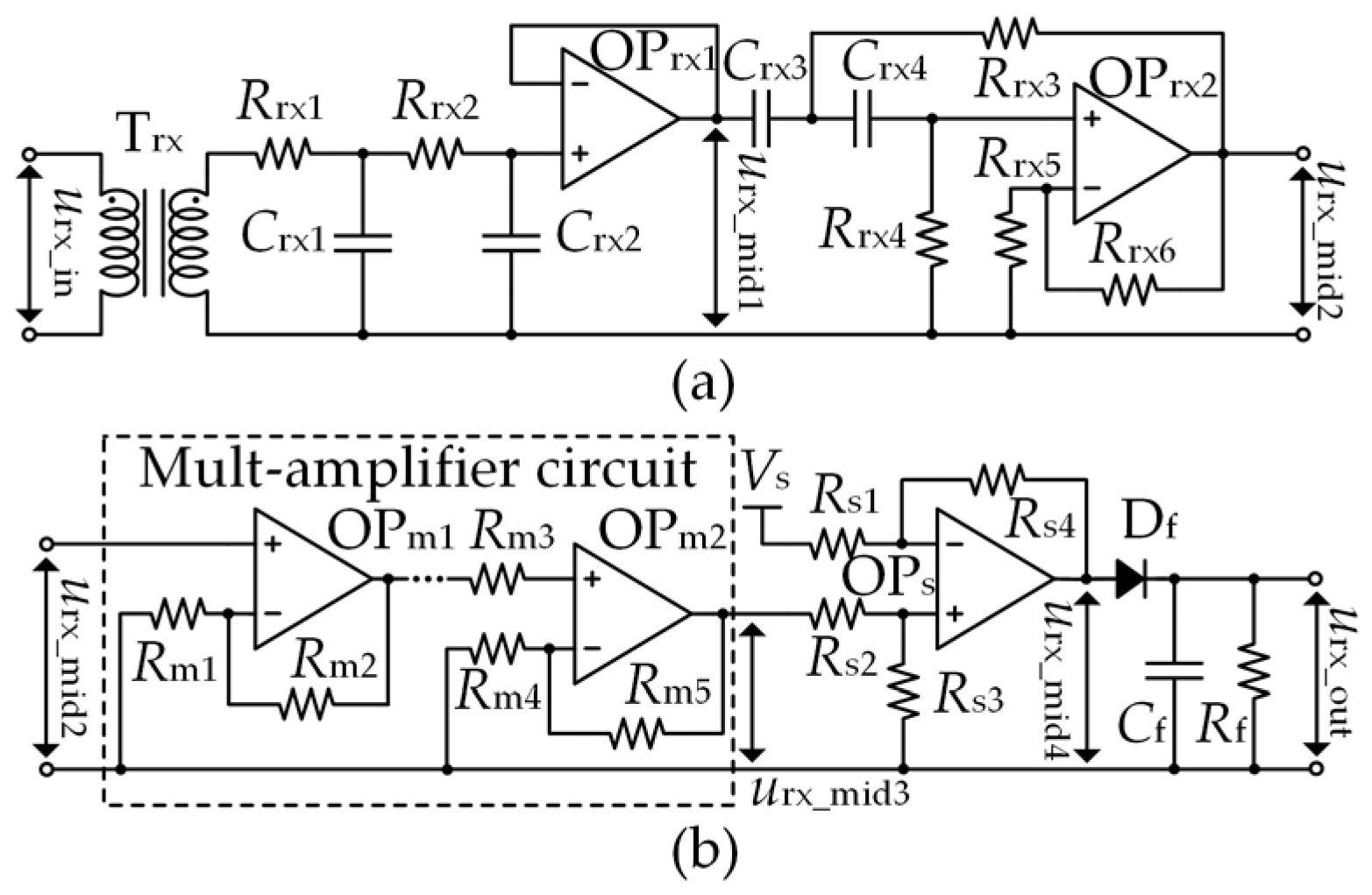
The signal receiving circuit of the system, as shown in Figure 10, consists of a filtering circuit, a multistage amplification circuit, a cross-talk suppression circuit, and a demodulation circuit.
The filtering circuit in the signal receiving circuit, as shown in Figure 10a, is a band-pass filter composed of a second-order low-pass filter and a second-order Butterworth high-pass filter. The voltages urx_mid1, urx_mid2, urx_mid3, and urx_mid4 are the intermediate signal of the signal circuit. urx_out is the output signal of the receiving side. Vs is the reference voltage of the cross-talk suppression circuit. Rs1, Rs2, Rs3, and Rs4 are resistors in the cross-talk suppression circuit. In the first-stage low-pass filter, the transfer function H1(s) between the intermediate-stage signal urx_mid1 and the input signal urx_in can be expressed as:
H 1 ( s ) = u rx _mid1 u rx _ in = 1 / Z rx1 s 2 + R rx1 C rx1 + R rx2 C rx2 Z rx1 s + 1 Z rx1
where:
Z rx1 = R rx1 R rx2 C rx1 C rx2
In the second-stage high-pass filter, the transfer function H2(s) between the intermediate-stage signal urx_mid2 and the intermediate-stage signal urx_mid1 can be expressed as:
H 2 ( s ) = u rx _mid2 u rx _mid1 = k s 2 s 2 + R rx3 C rx4 + R rx3 C rx3 + R rx4 C rx4 1 k Z rx2 s + 1 Z rx2
where:
Z rx2 = R rx3 R rx4 C rx3 C rx4 k = R rx6 R rx5
Considering the amplitude attenuation of the received signal during transmission, the subsequent stage incorporates several signal amplification circuits, as shown in Figure 10b. The gain Grx between the intermediate-stage signal urx_mid3 and the intermediate-stage signal urx_mid2 can be expressed as:
G rx = u rx _mid3 u rx _mid2 = 1 + R m 2 R m 1 n
where Rm1 and Rm2 are resistors in the receiving-side amplification circuit and n is the number of stages in the multistage amplification circuit.
Since it is impossible to fully ensure that the signal transmitting plates and receiving plates in the coupling mechanism are arranged completely symmetrically, the coupling mechanism does not achieve absolute same-side decoupling. The transmitting signal and the receiving signal have the same frequency, so the signal cross talk from one side to the other cannot be eliminated by the filtering circuit, as shown in Figure 11.
For the high-level part of the signal, since any level higher than the standard value is recognized as logic “1,” cross talk has no impact on it. However, for the low-level part of the signal, the presence of cross talk may cause the original logic “0” to be misinterpreted as logic “1,” thereby causing bit errors in the received signal. A cross-talk suppression circuit based on a subtractor is adopted to shift the signal waveform downward, and combined with a subsequent unidirectional diode, the low-level cross talk of the signal is eliminated. As shown in Figure 10b, the relationship between the intermediate-stage signal urx_mid4 and the intermediate-stage signal urx_mid3 is as follows:
V s + R s 1 u rx _mid4 V s R s 1 + R s 4 = R s 3 u rx _mid3 R s 2 + R s 3
Let Rs1 = Rs4 and Rs2 = Rs3. The relationship between the intermediate-stage signal urx_mid4 and the intermediate-stage signal urx_mid3 can be reexpressed as:
u rx _mid4 = u rx _mid3 V s
If Df is an ideal diode with an internal resistance of 0, the relationship between the system output signal urx_out and the input signal urx_in can be expressed as:
u rx _ out = H 1 s H 2 s G rx u rx _ in V s

4. Experimental Verification

4.1. Experimental Prototype

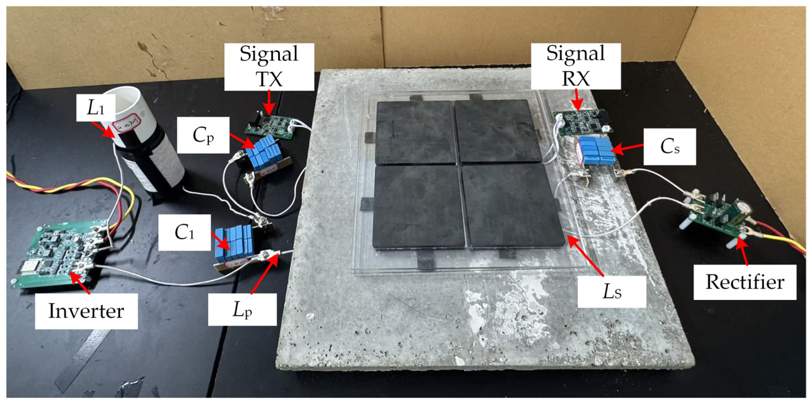
To verify the feasibility and effectiveness of the wireless power and signal transmission system proposed in this paper, an experimental prototype of the system as shown in Figure 12 was built, and the parameters of the prototype are listed in Table 1. In accordance with the circuit diagram illustrated in Figure 1, a magnetic-field coupling-based power transmission system and an electric-field coupling-based signal transmission system were constructed.
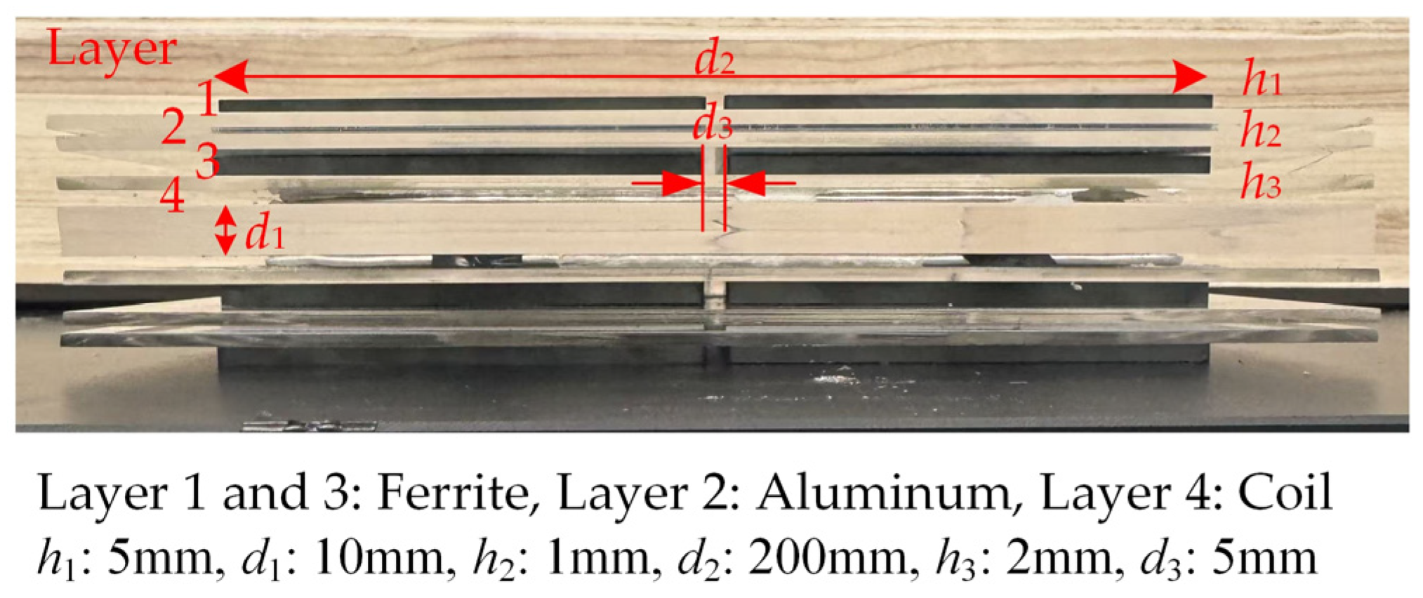
Figure 13 shows the side view of the coupler in the system. The coupler is composed of ferrite, aluminum plates, acrylic plates, and coils, where the thickness of the acrylic plates is fixed at 2 mm. Specifically, the dimensions of each layer are as follows: the ferrite in the first layer and the third layer have the same thickness, both being h1 = 5 mm; the thickness of the aluminum plate in the second layer is h2 = 1 mm; and the thickness of the coil in the fourth layer is h3 = 2 mm. Additionally, the air gap between the coils is d1 = 10 mm, the overall width of the coupler is d2 = 200 mm, the distance between the aluminum plate and the ferrite in the third layer is d3 = 2 mm, and the primary side and secondary side of the coupler have an identical structural design.
In Figure 14, the top view of the coupler can be divided into four layers from top to bottom, and adjacent layers are separated by acrylic plates with a thickness of 2 mm. For the specific top-view shapes and corresponding dimensions of each layer of the coupler, refer to Figure 14a–d.

4.2. Discussion of Experimental Results

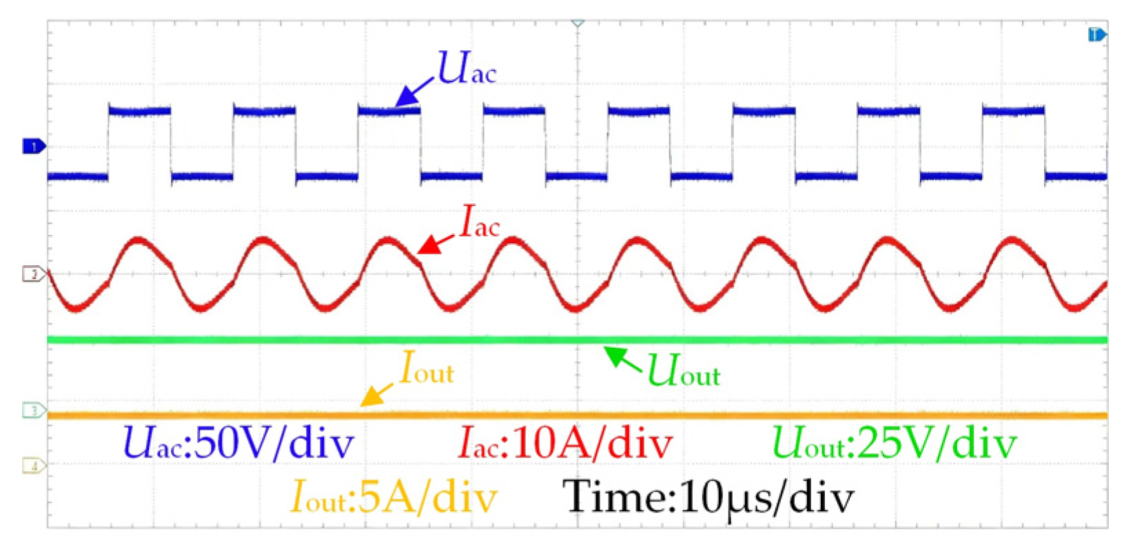
Figure 15 presents the key experimental waveforms of the wireless power transmission subsystem. The experimental waveforms show that when the system input voltage is 28 V, the operating frequency is 100 kHz, and the output DC load is 7.84 Ω, the waveforms of the inverter output voltage Uac, output current Iac, DC output voltage Uout, and DC output current Iout are recorded. From the inverter voltage and current waveforms, it can be seen that the system is well tuned and the current phase lags slightly behind the voltage phase, which proves that the system inverter operates in the zero-voltage switching (ZVS) state. In Figure 15, the output voltage of the system is 28.6 V and the output current is 3.62 A, from which it can be calculated that the output power of the system is 103.53 W. The overall power transmission efficiency of the system is measured to be 82%.
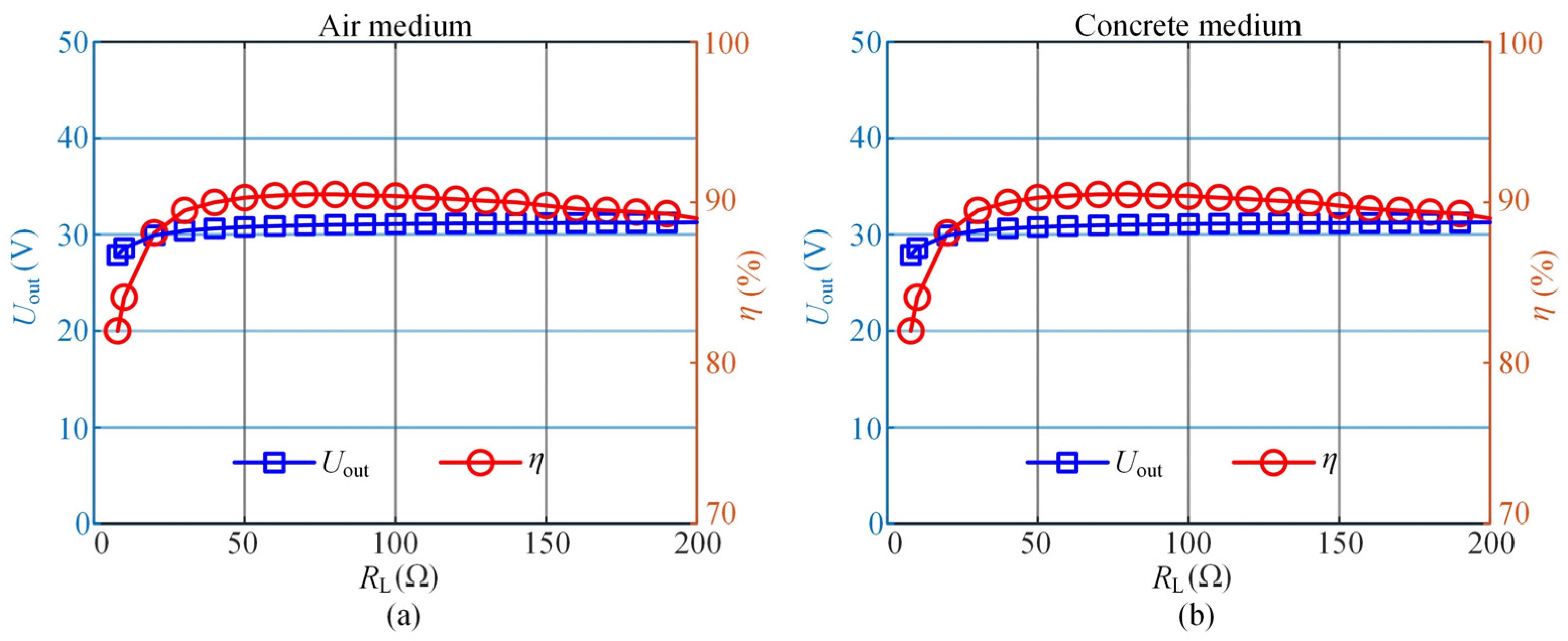
In this experiment, the DC input voltage was set to 28 V. As the load RL gradually increased from 7.84 Ω to 200 Ω, we simultaneously recorded the values of output voltage Uout and efficiency η. These measured values were plotted in the same scatterplot, as presented in Figure 16.
As shown in Figure 16, with the continuous increase in DC load, the output voltage shows a slow upward trend: it increases from the initial 27.87 V to 31.86 V, with a variation range of 14.3%. The system efficiency first increases from 82.1% under the rated load and peaks at 90.5% near RL = 70 Ω, then decreases slowly. When RL = 200 Ω, the efficiency drops to 86.7%. Meanwhile, a comparison between Figure 16a,b reveals that the values of system output voltage and efficiency are almost identical under the two media (air and concrete). This indicates that the power transmission characteristics of the concrete medium are similar to those of the air medium.
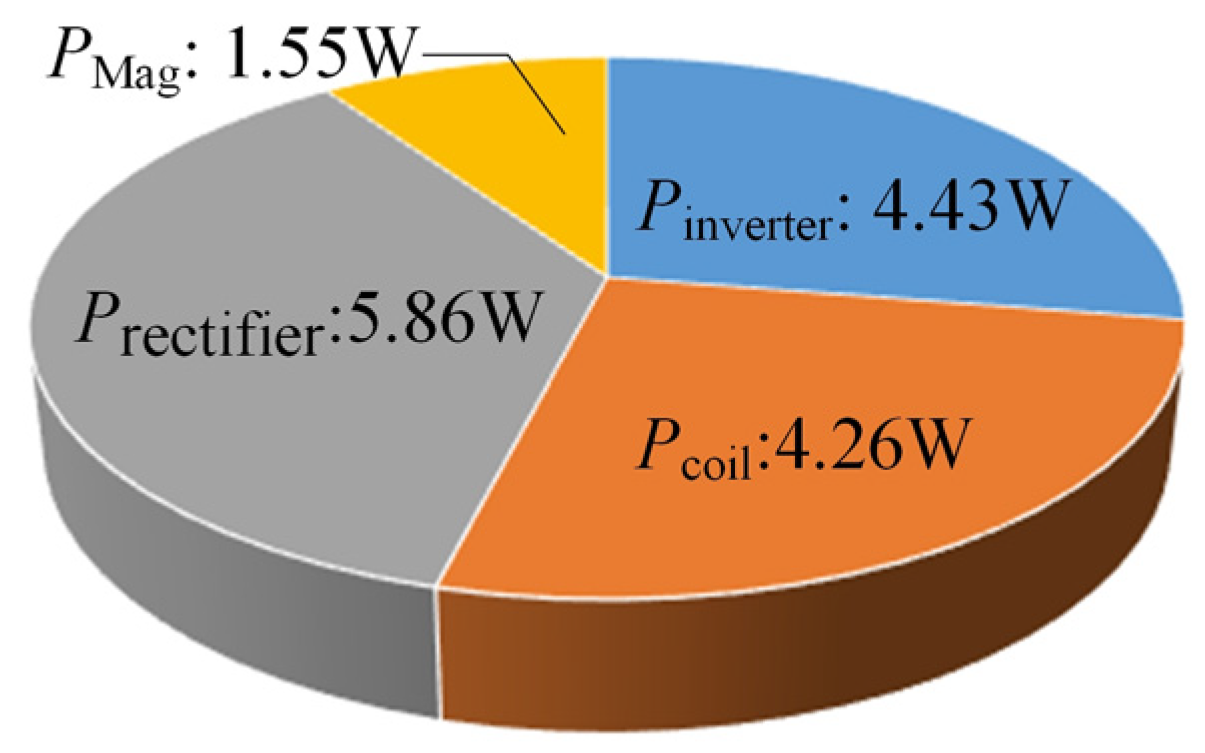
The sources of system losses are classified as follows: inverter losses Pinverter, copper losses Pcoil of the coil, coupling losses PMag caused by magnetic flux leakage, and rectifier losses Prectifier. The evaluation formulas for the losses are provided below.
The full-bridge inverter operates in the zero-voltage switching (ZVS)-ON state; therefore, only the conduction losses and turn-off losses of the inverter need to be considered. In the formula below, rDS represents the internal resistance of a single switch of the inverter; toff denotes the turn-off time; fₛ stands for the switching frequency; VF is the threshold voltage of a single diode; and rd refers to the conduction resistance of the diode. Then, the power losses on each part of the experimental prototype can be found from (23).
η = P out P out + P inverter + P coil + P rectifier + P coupler P inverter = 2 r DS I 1 ( rms ) 2 + 1 6 E dc I off t off f s P coil = I 1 ( rms ) 2 r 1 + I 2 ( rms ) 2 r 2 + I 3 ( rms ) 2 r 3 P rectifier = 2 V F I o + 2 r d I 3 ( rms ) 2 P Mag = P i n P out P inverter P coil P rectifier
Practical measurements were conducted on the experimental prototype built in this paper, and the parameters required for calculating the losses of each part of the prototype are shown in Table 2. By substituting these parameters into (23), we can obtain the loss of each part and their proportions in the total loss, as presented in Figure 17.
In terms of system efficiency, a circuit simulation model for the wireless power transfer part is established. Subsequently, the internal resistances of the coils r1, r2, and r3 are incorporated, the on-resistance rds of the MOSFET, and the forward voltage drop VF as well as internal resistance rd of the diode, into the simulation model. The parameter values are listed in Table 2, and the final comparison results between the efficiency simulation and experiment are presented in Table 3.
The results indicate that the voltage, current, and power of the system in the simulation are basically consistent with the values actually measured on the experimental prototype, with only some negligible deviations. On one hand, these deviations are jointly caused by measurement errors and simulation model errors. Regarding the measurement error, the oscilloscope used in the experiment is the KEYSIGHT DSOX3014T, with the voltage probe N2790A and current probe 1147B. All the aforementioned measurement instruments have completed zero-point calibration to ensure the reliability of the measured data. Additionally, the efficiency of the simulation model is 1.7% higher than that measured in the experiment. The main reason for this difference is that the simulation model does not account for losses such as the magnetic leakage loss of the inductive coupler and the switching loss of the inverter.
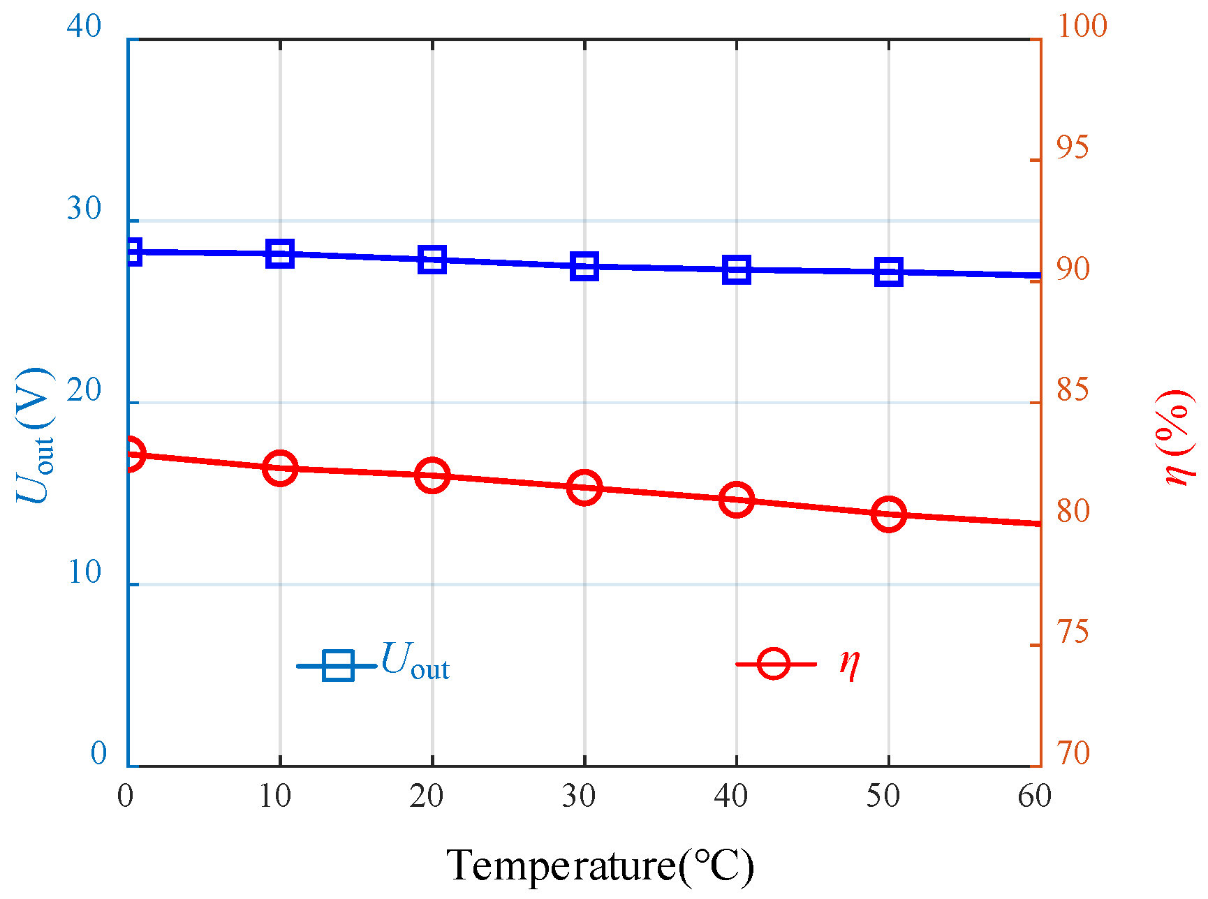
Temperature is also a potential factor that may affect the power transfer of the system. Concrete is a typical non-magnetic material, and its permeability is close to that of air. For ordinary concrete without ferromagnetic components, its relative permeability ranges from 1.0001 to 1.001, determined by constituent minerals with paramagnetic susceptibility (~10−5) and minimal temperature coefficient (~10−6/K). Even a 100 °C-temperature variation induces only ~10−4 relative permeability change, with negligible effect on magnetic coupling. Furthermore, the coupler’s magnetic core uses PC95 Mn-Zn ferrite, which maintains high, stable permeability within −40 °C to 100 °C (normal temperature range) due to orderly internal magnetic domain arrangement.
To verify temperature impact, experiments were conducted in a temperature-controlled chamber over 0–60 °C (matching actual operating range of embedded sensors). As shown in Figure 18, results show slight decreases in output voltage and efficiency with rising temperature (caused by increased system internal resistance), while overall stability is maintained.
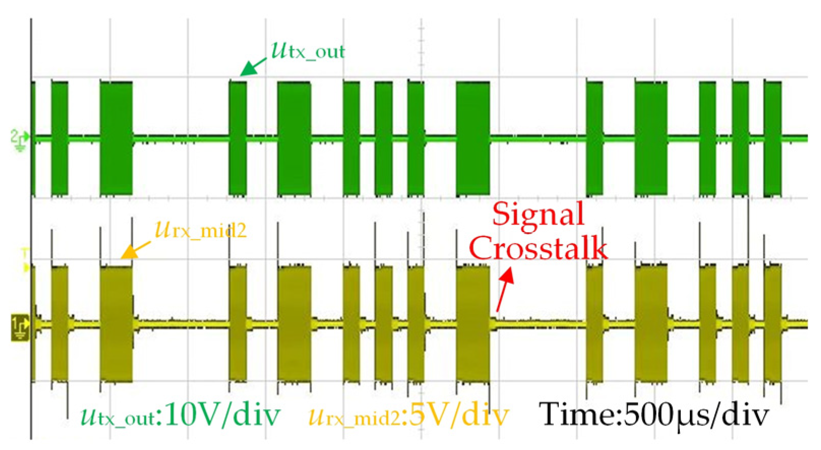
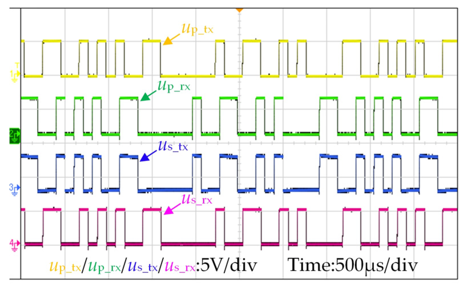
Subsequently, under the operating condition of simultaneous power and signal transmission, the waveform of the transmitted signal utx_out after ASK modulation on the primary side of the system and the waveform of the received signal urx_mid2 on the primary side after passing through the filter circuit were recorded, as shown in Figure 19. It can be observed that due to the fact that the coupler of the experimental prototype cannot be placed in a completely symmetrical manner in practice. A certain degree of signal cross talk still occurs at the signal transmission ports on the same side. After adding the subtractor-based cross-talk suppression circuit, the waveforms of the primary-side transmitted signal up_tx, primary-side received signal up_rx, secondary-side transmitted signal us_tx, and secondary-side received signal us_rx are shown in Figure 20. The figure shows that the waveforms of up_tx and us_rx and those of us_tx and up_rx are consistent. In addition, there is no clutter interference or bit error phenomenon, which proves that the modulation and demodulation functions of the signal circuit are normal.
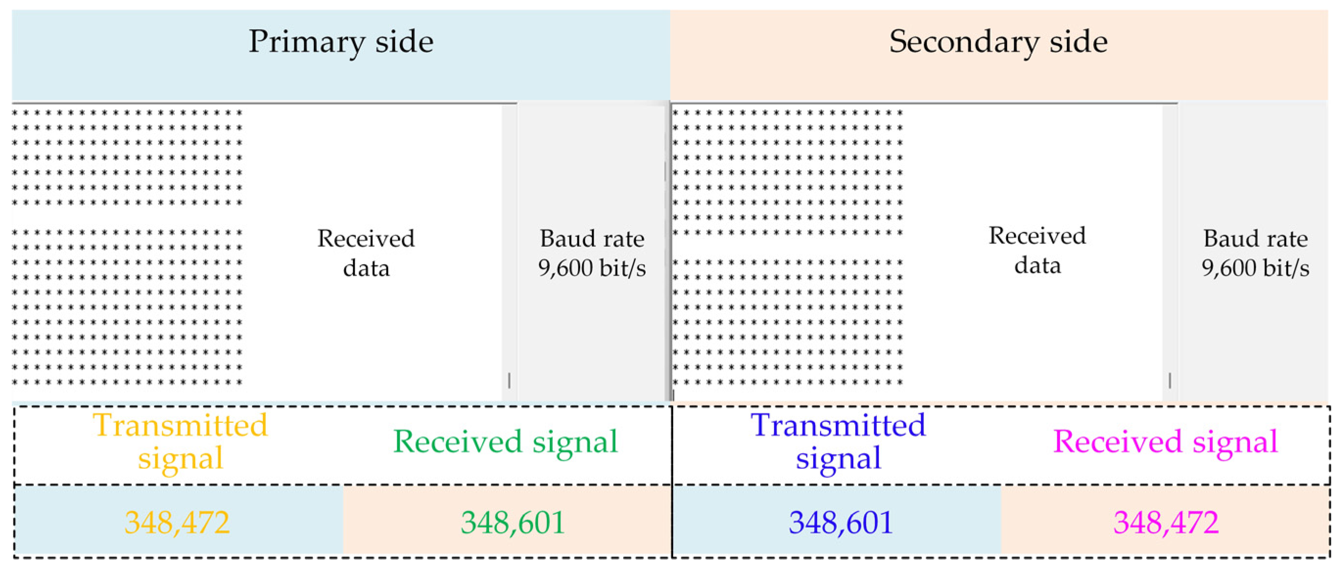
Subsequently, a serial port debugging assistant was used to test the accuracy of signal transmission and reception of the experimental prototype under the premise of wireless power transmission. The signal transmission results are as shown in Figure 21. The host computer was used to send a string composed of “*” characters and “space” characters to the primary side and secondary side. The host computer received the demodulated signals from the primary side and secondary side, and the number of transmitted and received characters as well as the bit error rate were recorded, as listed in Table 2.
In Figure 20, it can be seen that the demodulated signals of the primary side and secondary side received by the host computer are consistent with the transmitted signals from the host computer. In Table 4, it can be observed that in three consecutive communication tests with 300,000 characters each, the total number of transmitted characters is equal to that of received characters and the bit error rate (BER) is 0 in all cases, indicating that the entire communication module achieves normal full-duplex operation. In this experiment on simultaneous energy and signal transmission, the signal transmission module is not interfered with by the energy transmission module, realizing the decoupling of energy and signal. At the same time, the interference of the signal transmission modules on the same side is relatively small and can be eliminated by the cross-talk suppression circuit, thus achieving decoupling on the same side.
The core differences between the proposed method and existing hybrid or dual-channel wireless power and signal transmission schemes are summarized in Table 5, along with supplementary explanations of its innovation points.
According to the comparison in Table 5, this paper presents four key advantages. (1) The proposed method requires no additional design and relies solely on the natural decoupling of near-field electric and magnetic fields, distinguishing itself from existing schemes [19,23] that depend on complex high-performance filter circuits and [24,25] that rely on precision-decoupled coil structures. (2) It achieves bidirectional signal decoupling via a simple orthogonal structure of coupling plates, a feature that is not realized in existing methods. (3) The filter circuit adopted is simple, in contrast to the very complicated filter circuits in [19,23], while maintaining parity with the simple filter circuit design in [24,25] but with further structural advantages. (4) No additional components are needed in the coupler structure, unlike those in [24,25], which require additional signal coils, thus reducing hardware complexity and cost.

5. Conclusions

To solve the power supply and data transmission bottlenecks of pre-embedded sensors for concrete structure monitoring, this paper proposes a hybrid electric- and magnetic-field decoupled transmission technology for wireless power and full-duplex signals. It leverages the inherent decoupling of near-field electric and magnetic fields to construct independent power (magnetic field via coils) and signal (electric field via plates) channels, and achieves uplink–downlink data decoupling through orthogonal coupling plates. Mathematical models for power/signal channels and designs for power compensation networks and signal filtering circuits are established, with finite element simulations validating decoupling performance. Experimental results show the system realizes 100 W power transmission with 82% efficiency and full-duplex communication with 9600 bit/s bidirectional rate, with no bit errors in 300,000 bidirectional characters, providing a reliable solution for integrated power and data transmission of pre-embedded sensors. This technology is expected to be applied in bridge and tunnel scenarios to supply power and transmit data for embedded stress and temperature sensors. It can adapt to complex infrastructure operation and maintenance environments without the need for slotting or modification of concrete.

Author Contributions

Conceptualization, X.W. (Xiaolong Wang) and X.W. (Xiaozhou Wei); methodology, X.W. (Xiaolong Wang); software, X.W. (Xiaolong Wang); validation, X.W. (Xiaozhou Wei); investigation, X.W. (Xiaolong Wang); writing—original draft preparation, L.J.; writing—review and editing, X.W. (Xiaozhou Wei); visualization, L.J. All authors have read and agreed to the published version of the manuscript.

Funding

This research received no external funding.

Data Availability Statement

The original contributions presented in this study are included in the article. Further inquiries can be directed to the corresponding author.

Conflicts of Interest

Authors Xiaolong Wang, Xiaozhou Wei and Laiqiang Jia were all employed by the Lanzhou Power Supply Company, State Grid Gansu Electric Power Company. All authors declare that the research was conducted in the absence of any commercial or financial relationships that could be construed as a potential conflict of interest.

References

  1. Jing, B.; Wang, X.; Li, Y.; Liu, Y.; Zou, J.; Luo, X.; Liu, F.; Li, G. Frequency measurement method of vibrating wire sensor in complex noise environment. In Proceedings of the 2024 International Conference on Advanced Control Systems and Automation Technologies, Nanjing, China, 15–17 November 2024. [Google Scholar]
  2. Han, D.; Kim, K.; Shin, J.; Park, J. Gesture-based secure authentication system using triboelectric nanogenerator sensors. Sensors 2025, 25, 5170. [Google Scholar] [CrossRef] [PubMed]
  3. Peng, Y.; Ma, E.; Wang, Q.; Chen, Y.; Mai, R.; Madawala, U.K. Maximizing output power of inductive power transfer systems under rebar array shielding. IEEE Trans. Power Electron. 2024, 39, 13934–13945. [Google Scholar] [CrossRef]
  4. Peng, Y.; Qi, W.; Chen, Y.; Mai, R.; Madawala, U.K. Wireless sensor power supply based on eddy currents for structural health monitoring. IEEE Trans. Ind. Electron. 2024, 71, 7252–7261. [Google Scholar] [CrossRef]
  5. Zhang, J.; Ma, C.; Wang, Z. An Electro-Optic (EO) pulsed electric field sensor powered by photovoltaic cell. Phys. Scr. 2024, 99, 025001. [Google Scholar] [CrossRef]
  6. Mishra, M.; Lourenco, P.B.; Ramana, G.V. Structural health monitoring of civil engineering structures by using the internet of things: A review. J. Build. Eng. 2022, 48, 103954. [Google Scholar] [CrossRef]
  7. Almania, N.; Alhouli, S.; Sahoo, D. A photovoltaic light sensor-based self-powered real-time hover gesture recognition system for smart home control. Electronics 2025, 14, 3576. [Google Scholar] [CrossRef]
  8. Gouda, O.E.; Darwish, M.M.F.; Mahmoud, K.; Lehtonen, M.; Elkhodragy, T.M. Pollution severity monitoring of high voltage transmission line insulators using wireless device based on leakage current bursts. IEEE Access 2022, 10, 53713–53723. [Google Scholar] [CrossRef]
  9. Sajad, H.; Alireza, H. A novel self-powered, high-sensitivity piezoelectric vibration sensor based on piezoelectric combo effect. IEEE Sens. J. 2023, 23, 25797–25803. [Google Scholar]
  10. Niu, S.; Jia, Q.; Hu, Y.; Yang, C.; Jian, L. Safety management technologies for wireless electric vehicle charging systems: A review. Electronics 2025, 14, 2380. [Google Scholar] [CrossRef]
  11. Pahlavan, S.; Shooshtari, M.; Maleki, M. Using overlapped resonators in wireless power transfer for uniform electromagnetic field and removing blank spots in free moving applications. Electronics 2022, 11, 1204. [Google Scholar] [CrossRef]
  12. Pahlavan, S.; Shooshtari, M.; Jafarabadi Ashtiani, S. Star-shaped coils in the transmitter array for receiver rotation tolerance in free-moving wireless power transfer applications. Energies 2022, 15, 8643. [Google Scholar] [CrossRef]
  13. de SouzaGomes, Y.; Saidi, M.; Lushnikova, A.; Ple, O. Fibre Optic-based patch sensor for crack monitoring in concrete structures. Strain 2025, 61, e12489. [Google Scholar] [CrossRef]
  14. Yu, Y.; Dong, Y.; Jiang, Y.; Wang, F.; Zhou, Q.; Ba, P. Research on the defect detection method of steel-reinforced concrete based on piezoelectric technology and weight analysis. Sensors 2025, 25, 3844. [Google Scholar] [CrossRef] [PubMed]
  15. Zhang, Z.; Cheng, H.; Li, Z.; Chen, F.; Chen, Y.; He, Z.; Mai, R. Wireless sensor power supply for rotating shaft using DC-side diode array with stable output. IEEE Trans. Power Electron. 2024, 39, 15414–15419. [Google Scholar] [CrossRef]
  16. Qu, J.L.; He, L.X.; Tang, N.; Lee, C.-K. Wireless power transfer using domino-resonator for 110-kV power grid online monitoring equipment. IEEE Trans. Power Electron. 2020, 35, 11380–11390. [Google Scholar] [CrossRef]
  17. Yao, Y.; Sun, P.; Liu, X.; Wang, Y.; Xu, D. Simultaneous wireless power and data transfer: A comprehensive review. IEEE Trans. Power Electron. 2022, 37, 3650–3667. [Google Scholar] [CrossRef]
  18. Pajer, R.; Chowdhury, A.; Redic, M. Demodulation of feedback signal for wireless charging systems according to the Qi standard. In Proceedings of the 2018 25th International Conference on Systems, Signals and Image Processing, Maribor, Slovenia, 20–22 June 2018. [Google Scholar]
  19. Luo, Y.; Yang, Y.; Hong, H.; Dai, Z. A simultaneous wireless power and data transfer system with full-duplex mode for underwater wireless sensor networks. IEEE Sens. J. 2024, 24, 12570–12583. [Google Scholar] [CrossRef]
  20. Wang, Y.; Xie, S.; Chen, L. A capacitive power and signal transfer system based on ring-coupler with mitigated inter-channel crosstalk. Electr. Eng. 2024, 106, 343–352. [Google Scholar] [CrossRef]
  21. Liu, Y.; Zhang, J. Misalignment Tolerance Improvement and High Efficiency Design for Wireless Power Transfer System Based on DDQ-DD Coil. Int. J. Circuit Theory Appl. 2024, 52, 111–128. [Google Scholar] [CrossRef]
  22. Da, C.; Wang, L.; Li, F.; Tao, C.; Zhang, Y. Analysis of Undersea Simultaneous Wireless Power and 1 Mb/s Data Rate Transfer System Based on DDQ Coil. IEEE Trans. Power Electron. 2023, 38, 11814–11825. [Google Scholar] [CrossRef]
  23. Luo, B.; Wang, M.; Tang, J.; Wang, T.; Bai, L.; You, J. An Underwater Simultaneous Wireless Power and Analog-Digital Hybrid Signal Transfer System. IEEE Trans. Power Electron. 2025, 40, 17569–17574. [Google Scholar] [CrossRef]
  24. Fan, Y.; Chen, Q.; Wu, S.; Xiao, J.; Wang, Z. A Bidirectional Simultaneous Wireless Power and Data Transfer System with Non-Contact Slip Ring. Electronics 2024, 13, 3974. [Google Scholar] [CrossRef]
  25. Zhang, Z.; Liu, Y.; Wang, Z.; Mu, X.; Chen, J. Hybrid Beamforming Design for Near-Field SWIPT Networks. In Proceedings of the ICC 2024—IEEE International Conference on Communications, Denver, CO, USA, 9–13 June 2024; pp. 1807–1812. [Google Scholar]
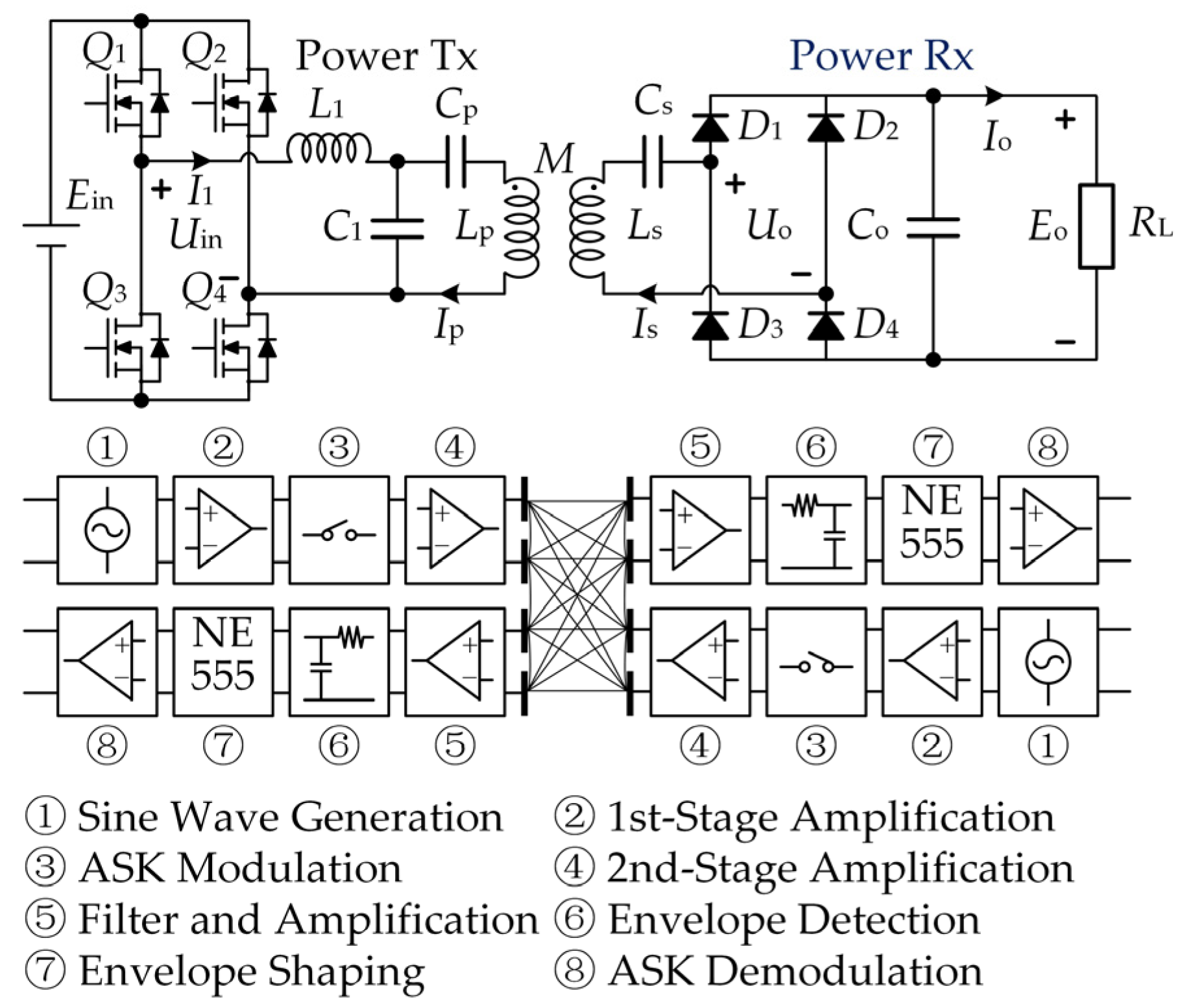
Figure 1. Block diagram of the proposed wireless power and signal transfer system.
Electronics 14 04302 g001
Figure 2. Side view of the electric- and magnetic-field hybrid coupler.
Electronics 14 04302 g002
Figure 3. Top view of structure and dimensions of the proposed coupler. (a) Outer ferrite layer, (b) aluminum plate, (c) inner ferrite layer, and (d) coil.
Electronics 14 04302 g003
Figure 4. Capacitive coupler for bidirectional signal transmission channel.
Electronics 14 04302 g004
Figure 5. Magnetic-field distribution cloud diagram of the proposed coupler.
Electronics 14 04302 g005
Figure 6. Electric-field distribution cloud diagram of the proposed coupler near the four plates on the (a) primary side and (b) secondary side.
Electronics 14 04302 g006
Figure 7. Circuit of LCC-S-based wireless power transfer system.
Electronics 14 04302 g007
Figure 8. Equivalent model of LCC-S-type resonant network.
Electronics 14 04302 g008
Figure 9. Circuit diagram of ASK modulation-based signal transmitter. (a) ASK modulation logic, (b) signal circuit based on ASK modulation.
Electronics 14 04302 g009
Figure 10. Signal receiving circuit of the system. (a) Fourth-order band-pass filtering circuit, (b) signal amplification and cross-talk suppression circuit.
Electronics 14 04302 g010
Figure 11. Same-side signal cross-talk schematic diagram.
Electronics 14 04302 g011
Figure 12. Photograph of the experimental prototype.
Electronics 14 04302 g012
Figure 13. Side view of the hybrid coupler of the prototype.
Electronics 14 04302 g013
Figure 14. Top view of the hybrid coupler of the prototype. (a) First layer, (b) second layer, (c) third layer, (d) fourth layer.
Electronics 14 04302 g014
Figure 15. Input and output waveforms of the wireless power transmission system.
Electronics 14 04302 g015
Figure 16. Relationship between Uout, η and RL under (a) air and (b) concrete medium.
Electronics 14 04302 g016
Figure 17. Power loss distribution of the experimental prototype.
Electronics 14 04302 g017
Figure 18. System output voltage and efficiency at different temperatures.
Electronics 14 04302 g018
Figure 19. Primary-side ASK modulation waveforms.
Electronics 14 04302 g019
Figure 20. Transmitted and received digital signal waveforms at primary and secondary side.
Electronics 14 04302 g020
Figure 21. Schematic diagram of transmitted and received signal results.
Electronics 14 04302 g021
Table 1. Main parameters of the experimental prototype.
ParameterDefinitionValueUnit
EinDC input voltage28.00V
fOperating frequency100.00kHz
L1Compensation inductor at primary side40.70μH
LpSelf-inductance of transmitting coil102.30μH
LsSelf-inductance of receiving coil106.40μH
MMutual inductance of the coupler60.67μH
C1Compensation capacitor at primary side62.20nF
CpCompensation capacitor for transmitting coil41.10nF
CsCompensation capacitor for receiving coil23.80nF
RLLoad resistor7.84Ω
Table 2. Data required for calculating the losses of each part of the prototype.
ParameterValueParameterValue
rds0.11 ΩVF0.7 V
toff3 × 10−7 srd0.05 Ω
ioff0.29 Aio3.06 A
i14.36 Ar10.08 Ω
i20.57 Ar20.17 Ω
i33.98 Ar30.17 Ω
Table 3. Comparison of parameters between simulation and experimental prototype.
ParameterSimulated ValueExperimental ValueUnit
Ein28.0028.00V
I14.294.36A
Uo28.0826.53V
Io3.583.77A
Pin120.12122.08W
Po100.53100.02W
η83.70%82.0%/
Table 4. Data transmission accuracy.
TestPrimary SideSecondary SideError Rate
Transmitted SignalReceived SignalTransmitted SignalReceived Signal
1348,472348,601348,601348,4720%
2327,561329,652329,652327,5610%
3356,325355,896355,896356,3250%
Table 5. Comparison of the proposed and existing methods: differences and advantages.
This Paper[19,23][24,25]
Power/Signal DecouplingNo additional design is required, relying only on the natural decoupling of the electric field and magnetic fieldRelies on complex filter circuitsRelies on precision-decoupled coil structures
Bidirectional Signal DecouplingSimple orthogonal structure of coupling platesNot realizedNot realized
Filter CircuitSimpleVery complicatedSimple
Coupler structureNo additional componentsNo additional componentsNo additional components
Disclaimer/Publisher’s Note: The statements, opinions and data contained in all publications are solely those of the individual author(s) and contributor(s) and not of MDPI and/or the editor(s). MDPI and/or the editor(s) disclaim responsibility for any injury to people or property resulting from any ideas, methods, instructions or products referred to in the content.