1. Introduction
In recent years, the increasing demand for pulse power generators within industrial applications has propelled advancements aimed at extending device lifespan, adopting all-solid-state configurations, reducing physical dimensions, and achieving high repetition rates [
1,
2,
3]. Critical performance metrics for pulse generators encompass output voltage, current, and pulse width. Moreover, the characteristics of the output pulse waveform, particularly the front edge and flat top, play a crucial role in determining the generator’s suitability for specific applications. For instance, these waveform features contribute to attaining elevated average electron energies in pulsed atmospheric discharge plasmas [
4], accelerating ionization processes in atmospheric pressure plasma jets [
5], and improving the activation efficiency of Staphylococcus aureus [
6], etc.
The switch constitutes a fundamental element within pulse power generators, with its operational characteristics exerting a direct impact on the generator’s output power, operational lifespan, repetition rate, and the quality of the pulse waveform. Gas and magnetic switches, known for their high voltage- and current-handling capabilities, lack the ability to independently interrupt the circuit once triggered. To produce quasi-square output waveforms, pulse-forming lines (PFLs) and pulse-forming networks (PFNs) are frequently utilized for waveform-shaping purposes. Among these, PFNs have attracted considerable interest owing to their compact design and modularity, establishing them as essential components in the development of compact solid-state pulse-formation circuit units [
7].
Conventional high-power pulse-forming network (PFN) generators are predominantly regulated using gas switches. These switches present benefits including high power handling capability, low cost, minimal impedance, and reduced inductance; however, their operational lifespan, stability, and repetition rate remain constrained [
8]. To mitigate these limitations, numerous studies have explored the replacement of gas switches with magnetic switches. While this substitution enhances lifespan and stability, it introduces the requirement for a high-voltage reset circuit. Furthermore, the saturation inductance inherent to magnetic switches continues to influence the pulse front characteristics. Attempts to diminish the effects of saturation inductance by enlarging the magnetic core volume result in substantial increases in the generator’s size, cost, and weight [
9,
10]. Recently, pulse generators utilizing saturable pulse transformers (SPT) have attracted considerable interest due to their capacity for high voltage and current, compact configuration, and dual role as both transformer booster and magnetic switch. Rong Chen et al. [
11,
12] examined a PFN pulse generator employing SPT-based anti-resonance, which circumvented the drawbacks of gas switches and produced square wave outputs via an anti-resonance network. Nonetheless, the pulse front edge duration exceeded 1 microsecond at output peak voltages of 18.5 kV and 29 kV. Additionally, achieving optimal impedance matching necessitated variation in the capacitances within the anti-resonant network. Xiao Liu et al. [
13] investigated a Blumlein PFN pulse generator incorporating an SPT, utilizing a magnetic switch as the principal control element to sharpen the pulse front edge; however, the pulse front edge duration remained above 100 ns at a peak output voltage of 13.2 kV. Similarly, Longyu Zhuang et al. [
14] studied a Blumlein PFN pulse generator based on SPT, which attained a fully solid-state design alongside enhanced output pulse stability and repetition frequency. Despite these advancements, the influence of SPT saturation inductance on the pulse front edge constrained the achievable output voltage, thereby limiting the generation of high currents. In summary, the current stage of research faces several challenges: pulse fronts occurring on the microsecond scale, difficulties in increasing voltage through series stacking, semiconductor control switches needing to withstand high voltage and current, and the saturation inductance of SPT significantly affecting the output pulse front, among other issues.
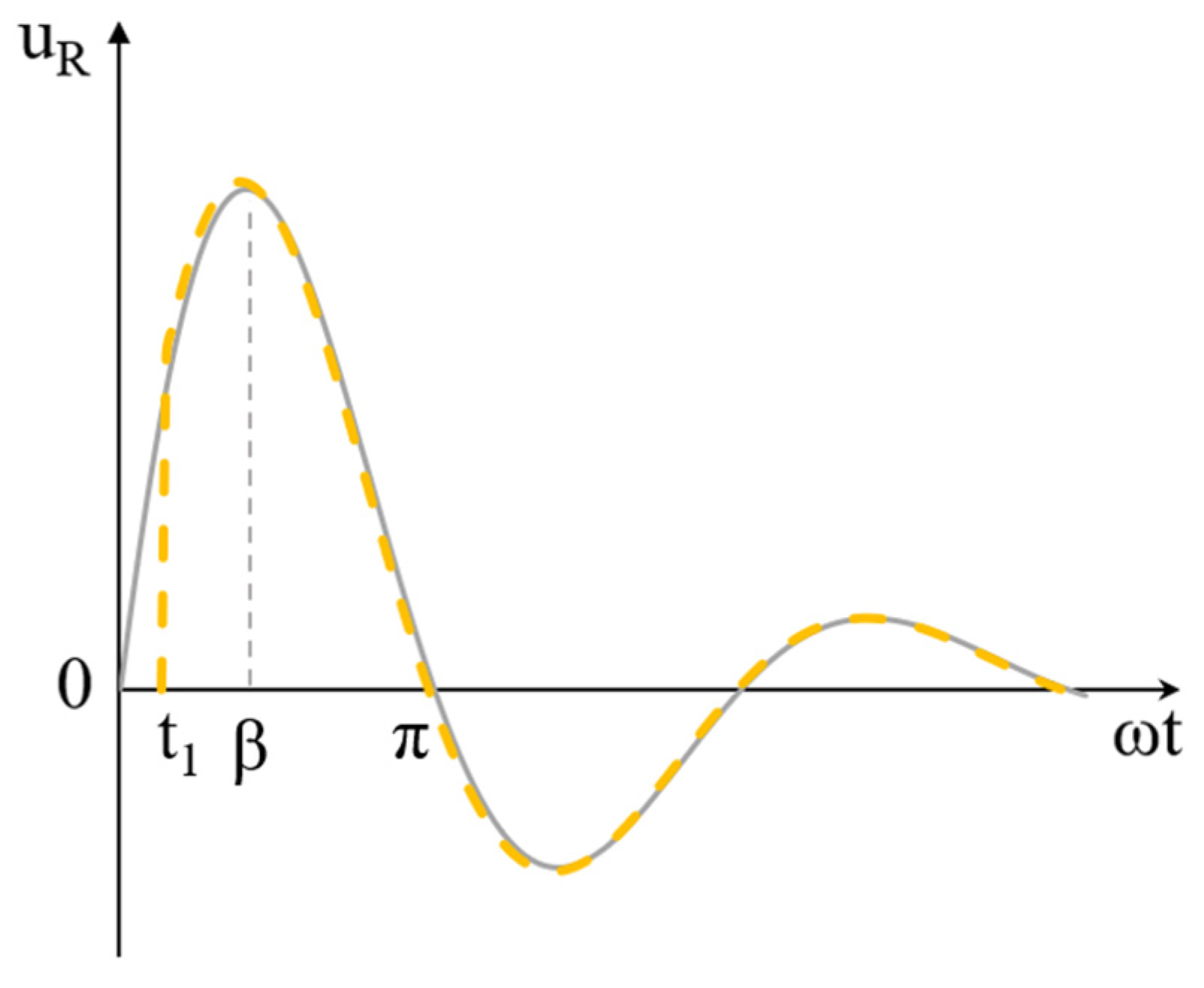
The conventional technique for enhancing the sharpness of the pulse front edge typically involves the use of magnetic switches [
15] or spark gap switches [
16] to block voltage, followed by the rapid closure of the switch under controlled conditions to deliver a pulse with a relatively steep rising edge to the load. Nevertheless, this method does not adequately address the effects of inductance within the circuit loop; furthermore, the inherent conduction delay and inductance of the switch itself tend to decelerate the pulse front edge. To overcome these limitations, the present study employs a cut-out switch to short-circuit the load during the initial discharge phase. Once the stray inductance in the circuit carries a certain current, the cut-out switch is promptly opened, enabling the capacitors to discharge swiftly into the load and thereby producing a pulse with a comparatively short front edge. This pulse-sharpening strategy effectively mitigates the influence of switch delay and jitter on the pulse front while also compensating for the impact of loop inductance. Moreover, situating the switch outside the discharge circuit prevents its inductance and resistance from adversely affecting the discharge process. The semiconductor open-circuit switch (SOS) is a specialized diode capable of interrupting currents on the order of 10 kA/cm
2 within tens of nanoseconds. However, pulse generators based on SOS technology exhibit several constraints that limit their practical application [
17,
18]. Firstly, the SOS operates as a nonlinear device, complicating the theoretical analysis of its output characteristics. Secondly, as a specially engineered high-voltage component, the performance of SOS devices can vary significantly, even among units of the same model. Thirdly, compared to conventional fast recovery diodes, SOS devices are generally more costly and larger in size.
To overcome the challenges associated with prolonged pulse rise times, low operational frequencies, and constrained output power in PFN pulse generators, this study introduces a novel PFN pulse generator architecture, incorporating a saturable pulse transformer (SPT) alongside fast recovery diodes. Initially, the SPT serves a dual function: it acts as a voltage-boosting transformer and simultaneously operates as a magnetic switch to regulate the discharge process. Moreover, the SPT’s saturated inductance is utilized as the inductive element within the first LC section on the PFN’s input side, thereby minimizing its influence on the front edge of the output pulse. Secondly, the implementation of conventional fast recovery diodes, exemplified by silicon-on-sapphire (SOS) diodes, effectively sharpens the pulse’s front edge. This strategy mitigates the adverse effects of switching delays and jitter, as well as diminishes the impact of loop inductance. Positioning the diode external to the discharge circuit further prevents its intrinsic inductance and resistance from interfering with the discharge dynamics. Through these circuit optimizations and the strategic selection of components, the pulse generator achieves output pulses characterized by rapid rise times, elevated voltage levels, substantial current amplitudes, narrow pulse widths, and high repetition rates, all while operating at relatively low charging voltages. Thirdly, the design facilitates modular scalability, wherein all modules share a common primary charging circuit, and the PFNs on the SPT’s secondary side are connected in series. This configuration enhances the output voltage amplitude without compromising the integrity of the pulse’s front and trailing edges, ensures synchronized charging across modules, simplifies the overall control scheme, and reduces system costs. Consequently, the PFN pulse generator developed with the integration of SPT and fast recovery diodes fulfills the criteria of an all-solid-state system, delivering pulses with short rise times, high voltage and current, brief pulse durations, compact form factor, cost-effectiveness, high repetition frequency, and quasi-square waveform characteristics.
Section 2 provides a detailed introduction to the proposed all-solid-state PFN pulse generator, emphasizing its short front edge and underlying operating principle.
Section 3 presents the simulation results, while
Section 4 discusses the experimental demonstration outcomes along with relevant analyses. Finally,
Section 5 offers the concluding remarks.
3. Simulation Study of the Pulse-Forming Network (PFN) Pulse Generator
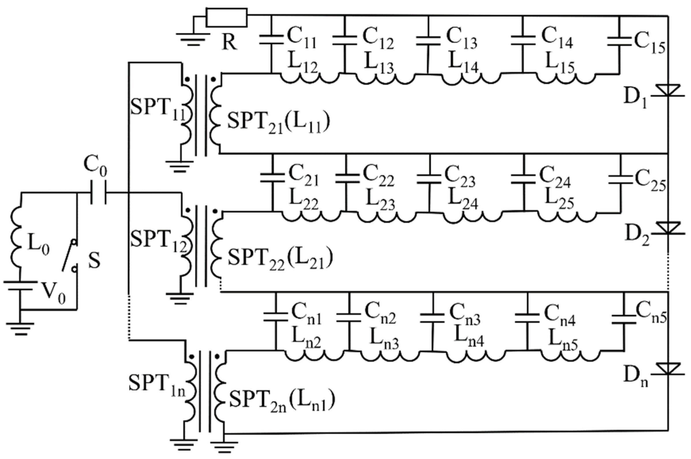
Using the circuit parameters obtained from theoretical calculations, we simulated the circuit shown in
Figure 4 with LTspice. The purpose of this simulation was to validate the accuracy of the theoretically derived parameters, clarify the operating principles of the pulse-forming network (PFN) generator, and investigate the mechanism and effectiveness of pulse front edge sharpening. In the configuration illustrated in
Figure 4, switch S
2 controls the saturation conduction state of the magnetic switch, while L
SPT denotes the saturation inductance of the SPT. Additionally, the sharpening switch S
3 regulates the current flowing through the inductor in the discharge circuit during PFN discharge to the load. To approximate realistic output conditions and enable comparison—considering that the simulation assumes an ideal, lossless environment—the transformation ratio of the SPT was set to 1:10. All other experimental parameters were kept consistent with those established in the previous chapter.
Figure 5 and
Figure 6 present the voltage and current waveforms derived from the simulation of the circuit depicted in
Figure 4, conducted under a charging voltage of 1 kV and a matching load resistance of 27 Ω.
Figure 5a shows the voltage and current waveforms observed on the primary side of the SPT, while
Figure 5b depicts the corresponding waveforms on the secondary side. The peak voltage measured on the primary side is 950 V, which is slightly lower than the power supply voltage. This reduction is attributed to the effect of the charging inductance within the primary charging circuit. In contrast, the peak voltage on the secondary side reaches 10 kV. This elevated voltage results from the simulation’s assumption of negligible resistance in the charging circuit, allowing the energy stored in the primary capacitor C
0 to be fully transferred to the secondary side. Throughout the energy transfer process from the primary to the secondary side, the current on the secondary side remains approximately proportional to that on the primary side.
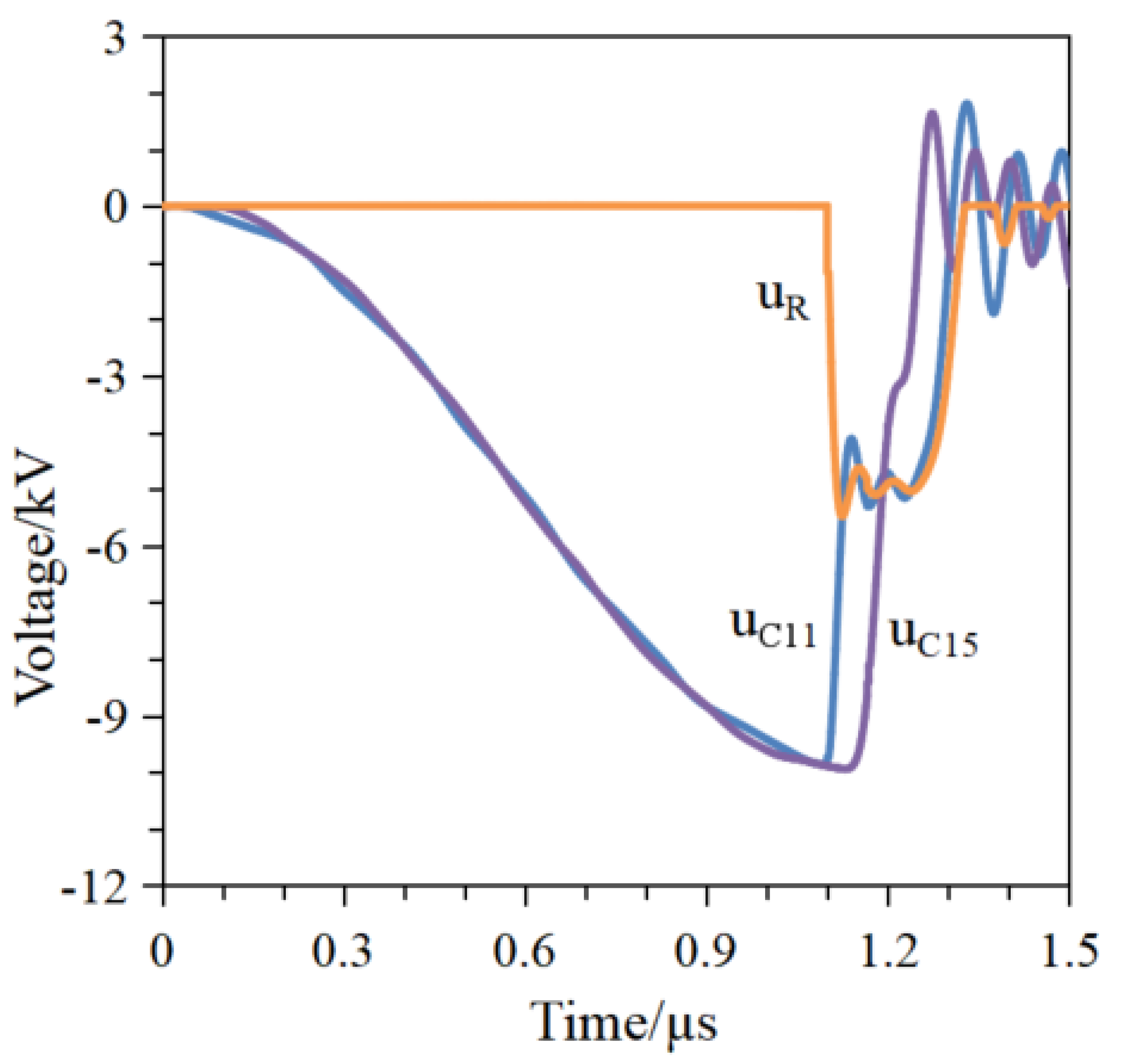
Figure 6 presents the voltage waveforms recorded from a single module across capacitors C
11 and C
15 and resistor R. As shown, all capacitors within the pulse-forming network (PFN), specifically C
11 through C
15, are charged synchronously to approximately −10 kV within about 1 μs. Due to resistance matching, the PFN produces nearly square high-voltage pulses at the load following the saturation of the saturable pulse transformer (SPT). The module generates a pulse with a peak voltage of −5.47 kV, a pulse width at half-maximum of 190 ns, and a rise time (10% to 90%) of 20 ns when connected to a 27 Ω matched load. The time required for the voltage to rise from zero to its peak is measured at 30 ns, closely aligning with the theoretically calculated value of 29.37 ns. Furthermore,
Figure 6 shows that the voltage rise and fall at the load are closely synchronized with the capacitor nearest the load. This occurs because the PFN discharge initiates from the capacitor adjacent to the load end, with the discharge sequence progressing sequentially from the capacitor farthest from the load toward the load end. Consequently, the front and trailing edges of the PFN output pulse are predominantly influenced by the LC unit closest to the load.
The saturable pulse transformer (SPT) not only amplifies voltage but also functions as a magnetic switch that controls the discharge process. However, increasing the voltage amplification ratio and the number of winding turns results in a higher saturable inductance. Therefore, it is essential to investigate how varying levels of SPT saturation inductance influence the characteristics of the output pulse.
Figure 7 illustrates the voltage waveforms across the load for different saturation inductance values (L) of the SPT. Since inductance impedes the current rise—with greater inductance exerting a stronger inhibitory effect—
Figure 7 shows that, although load voltage fluctuations and overshoot decrease as the SPT saturation inductance increases, the rise and fall times of the pulse edges correspondingly lengthen. The simulated output voltage pulse edges closely match theoretical predictions, confirming the consistency between simulation and analytical results.
Through simulation analysis, the pulse front-sharpening technique was employed to induce varying currents in the inductor, which subsequently discharged into the load. As illustrated in
Figure 8, the voltage waveform across the matched load varies with different current levels in the 2-μH inductor. When the current is below 185 A (defined as half of the capacitor voltage divided by the load), the front edge of the voltage waveform shortens as the current increases. However, once the current surpasses 185 A, the front edge remains essentially constant despite further increases in current. This phenomenon occurs because the front edge is primarily governed by the switching speed of the sharpening switch. Notably, as the current increases, the magnitude of the voltage overshoot on the load also increases. At a current of 185 A in the inductor, the front edge attains its minimum duration, and the output voltage exhibits no overshoot.
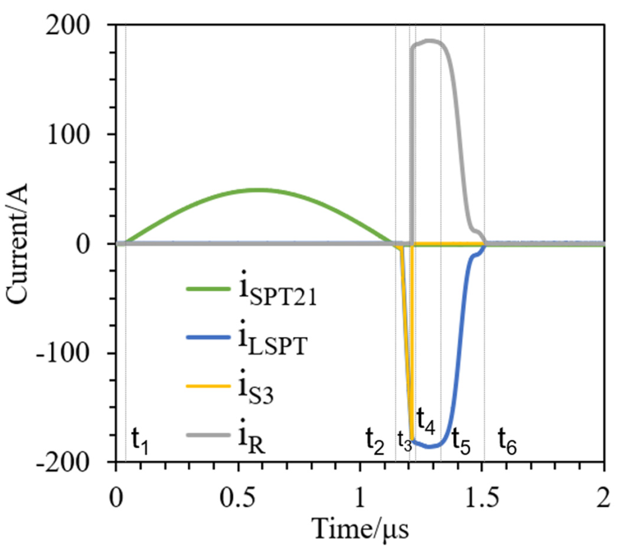
Figure 9 illustrates the current waveforms through the saturated inductor L
SPT, the sharpening switch S
3, and the load resistor R under optimal sharpening conditions, where the current in the L
SPT reaches 185 A. During the charging phase (t
1 to t
2), the sharpening switch S
3 is forward-biased, allowing current to flow sequentially through the SPT and diode D
1 to charge the primary energy storage capacitor, while the load resistor R is effectively short-circuited. This configuration prevents the occurrence of pre-pulses across the load. In the sharpening phase (t
2 to t
3), both switch S
2 and the sharpening switch S
3 are engaged, directing the entire current passing through the L
SPT to flow through the sharpening switch. This action increases the current in the saturated inductor L
SPT, while the load resistor R remains short-circuited, thereby avoiding the generation of excitation voltage. During the load current rise phase (t
3 to t
4), corresponding to the interval from the activation to the complete turn-off of the sharpening switch S
3, the current through S
3 rapidly diminishes as the load current correspondingly increases. Upon full disconnection of S
3, the current through the inductor L
SPT flows entirely through the load. In the stable load current output phase (t
4 to t
5), the PFN delivers a steady current, with all current sequentially passing through the inductor L
SPT and the load resistor R. During the load current decline phase (t
5 to t
6), the current flows sequentially through the SPT and the load resistor R, accompanied by a decrease in the voltage of the main energy storage capacitor, resulting in a reduction in the output current. Under optimal sharpening conditions, specifically, when the inductor current matches the output current, the front edge of the output pulse is predominantly governed by the turn-off speed of the sharpening switch S
3.
Figure 10 illustrates that the reverse current of the sharpening switch S
3 reaches 185 A. The output voltage waveform varies with different values of the saturation inductance (L
SPT). The effectiveness of the pulse front edge-sharpening technique was evaluated by comparing the output voltage waveforms with and without the sharpening switch, as shown in
Figure 7. The analysis yielded the following findings: (1) The pulse front edge-sharpening method effectively mitigates the impact of SPT saturation inductance on the pulse front edge, preventing any increase in the pulse front edge duration as the saturation inductance rises. (2) An increase in the saturation inductance of the SPT corresponds to a reduction in both overshoot and jitter of the output pulse; when the saturation inductance reaches or exceeds 2 μH, the output pulse exhibits negligible jitter and overshoot. (3) Implementation of the pulse front edge-sharpening technique results in a consistent half-height pulse width; however, as the saturation inductance increases, the flat-top width of the pulse progressively narrows at an accelerating rate. (4) The trailing edge of the output pulse lengthens as the saturation inductance of the SPT increases, which aligns with the predictions derived from the trailing edge formula.
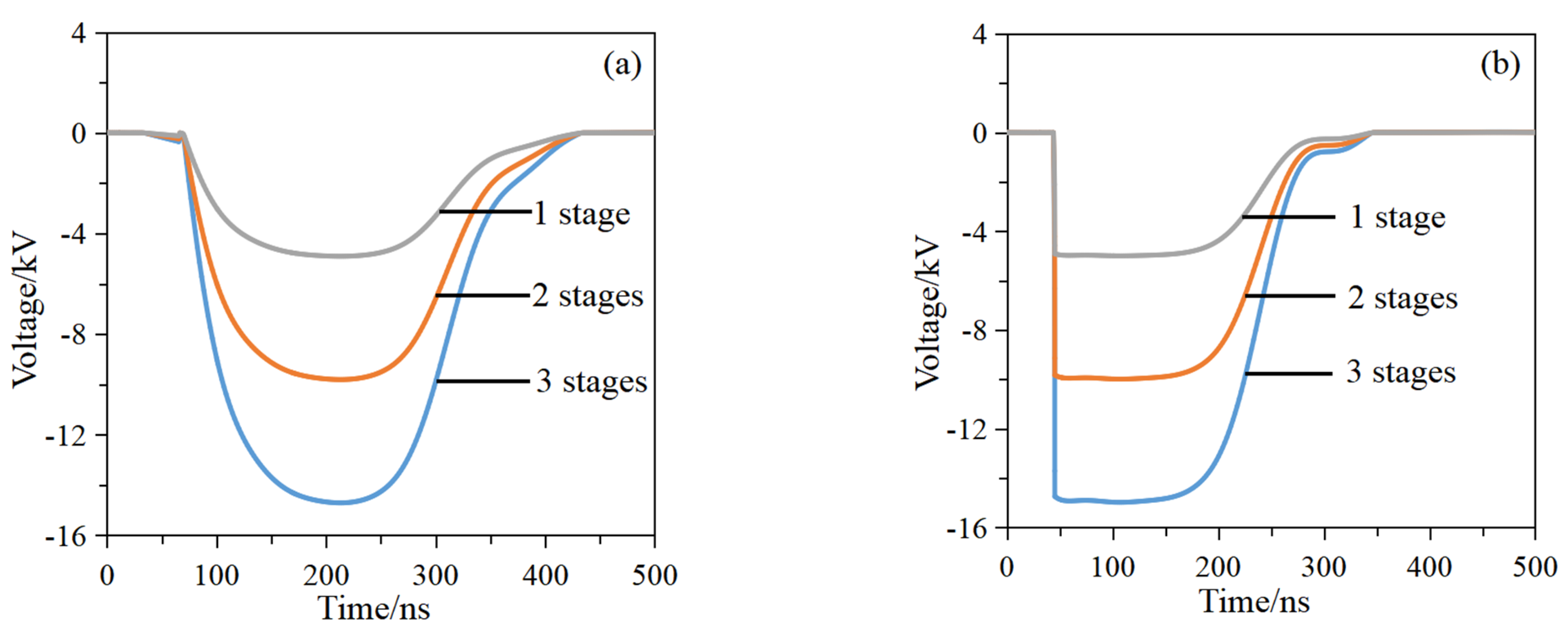
Figure 11a,b depict the output voltage waveforms across the matching load when modules 1, 2, and 3 are charged to 1 kV, with the SPT saturation inductance set at 2 μH, both with and without the pulse front-sharpening technology. The peak output voltage remains consistent regardless of the implementation of the pulse-front sharpening technique. This behavior can be attributed to the fact that the front edge of the output pulse from the PFN generator is primarily governed by the discharge characteristics of the LC units closest to the load. According to the theoretical expressions governing the pulse front and trailing edges, both the front edge fall time and the trailing edge rise time are directly proportional to the LC parameters. Consequently, the application of the pulse front-sharpening technology does not affect the increase in the front and trailing edge durations as the number of stages in the PFN pulse generator increases. Nevertheless, the use of the pulse front-sharpening method significantly reduces the pulse front edge duration (10~90%) from 71 ns to 5 ns. This improvement occurs because, under optimal sharpening conditions, the pulse front edge is predominantly determined by the switching speed of the sharpening switch. Importantly, this pulse generator design enables voltage multiplication through stage superposition without affecting the quality of the output pulse.
4. Experimental Results and Analysis
A prototype comprising three modules was developed for experimental evaluation to validate the accuracy of theoretical predictions and simulation results. The primary energy storage element is a 0.6-μF film capacitor, charged by a high-voltage DC power supply. On the primary side, the main control switch consists of three thyristors connected in parallel to enhance current-handling capability. The selected MOS gate-controlled thyristor is the IXYS IXHH40N150HV (CA), rated at 1.5 kV and 3.5 kA, manufactured by IXYS Corporation (CA). Each thyristor is driven by a dedicated driver-integrated circuit (MAX4420). These switches are the only circuit components requiring external signal control, as the secondary side circuitry is governed by magnetic switches incorporating pulse transformer functionality. The transformer core used is a 1K107 type, produced by Liyuan Electronics (Sichuan, China), with dimensions of 130 mm for the outer diameter, 85 mm for the inner diameter, and 13 mm thickness. The core exhibits magnetic properties characterized by a coercive force of 0.45 A/m, a saturation flux density of 0.75 T, and a residual flux density of 0.7 T. The magnetic core is reset using a direct current of 3 A.
In the secondary circuit, the 0.5 μH inductor is a custom-fabricated air-core coil. The capacitor used is a 0.7 nF ceramic capacitor rated for 30 kV made by Vishay 715C15KT (Malvern, Westborough, MA, USA). The fast recovery diode assembly consists of three sets, each containing two R400 diodes connected in parallel, with these sets arranged in series. This diode configuration provides a blocking voltage of 4 kV and a maximum peak surge current of 30 A and is manufactured by Sunmate Electronics (Guangdong, China).
Voltage measurements were conducted using the PMK PHV 4002 voltage probe (PMK Mess-und Kommunikationstechnik GmbH, Bad Soden am Taunus, Germany), while current measurements were obtained with the Pearson 110 current transformer (Pearson Electronics, Palo Alto, CA, USA). All waveform data were captured and recorded using the LeCroy Wavesurfer 3054Z oscilloscope (Teledyne LeCroy, Chestnut Ridge, NY, USA).
Figure 12 illustrates the operational mechanism of diodes. Initially, carriers are injected into the diode as the forward charging current flows through it. When the voltage polarity across the diode is reversed, a reverse current flows during the extraction of these carriers. The diode turns off once all carriers have been removed. Notably, the turn-off process occurs significantly faster than the carrier extraction phase. Fast recovery diodes, in particular, act as semiconductor open switches characterized by rapid turn-off speeds. Consequently, the fast recovery behavior of these diodes under reverse current conditions can be effectively utilized to sharpen the front edges of pulses.
Figure 13a,b depict the voltage and current waveforms on the primary and secondary sides of the SPT, respectively. The peak voltages observed on the primary and secondary sides are 850 V and 10 kV, respectively. These peak voltages are slightly lower than the charging voltage, due to the effects of the switch’s on-resistance and the loop inductance. Additionally, the resistance and inductance within the charging circuit cause a pronounced transient variation in the primary side voltage of the transformer at the onset of discharge. During the energy transfer from the primary to the secondary side, the current on the secondary side remains approximately proportional to that on the primary side.
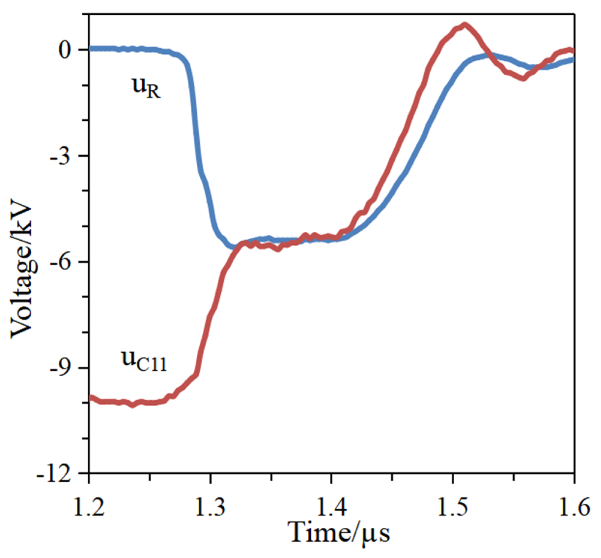
Figure 14 shows the voltage waveforms recorded across capacitor C
11 and the resistor R within a single module. Under matched load conditions, when the transformer core saturates, the PFN generator produces nearly square high-voltage pulses across the load. Specifically, one module delivers a peak voltage of −5.67 kV across a 27 Ω matching resistor, with a pulse width of 180 ns at half-maximum and a front edge duration of 19 ns measured between 10% and 90% of the pulse amplitude.
Figure 15 presents the experimentally obtained current waveforms of the SPT, diode D, and load resistor R. The experimental data demonstrate that incorporating a fast recovery diode significantly reduces the time required for the output current to reach its peak value, decreasing from 95 ns (t
2 to t
4) to 35 ns (t
3 to t
4). Additionally, the rise time of the pulse front edge shortens from 50 ns to 19 ns (10–90%). A comparative analysis of
Figure 9 and
Figure 14 reveals that the operational behavior of the pulse generator during experimentation closely aligns with the simulation results. However, the experimentally observed output pulse front edge exhibits a longer duration than predicted by the simulation, attributable to the reverse turn-off speed limitations of the fast recovery diode used in the experiment. Furthermore, the diode’s reverse peak current is slightly lower than the output current, a phenomenon primarily influenced by the diode’s reverse conduction interval and the saturation inductance inherent to the SPT. Notably, during the transition from the diode’s reverse turn-off to its complete cessation of conduction, the current within the saturated SPT continues to increase. Consequently, to prevent overshoot, the diode’s reverse peak current must remain below the output peak current. Moreover, the front edge of the output pulse is governed by the diode’s behavior throughout the entire reverse turn-off phase until full turn-off is achieved.
The pulse front-sharpening technology addresses not only the adverse effects of conduction delay and switch jitter on the pulse front but also mitigates the influence of stray inductance within the circuit loop. Notably, the sharpening device is positioned external to the discharge circuit, thereby avoiding the detrimental impact of stray inductance and conduction delay on the output pulse waveform. The efficacy of this pulse front-sharpening technique has been demonstrated through theoretical analysis, numerical simulations, and experimental validation. Optimal sharpening conditions are achieved when the sharpening switch is fully turned off, precisely as the inductor current reaches the final output current. Under these circumstances, the capacitor, charged to a specific voltage, and the inductor, carrying a defined current, simultaneously discharge into the load. Consequently, the pulse front edge is predominantly governed by the turn-off speed of the sharpening switch. Experimental limitations were observed due to the reverse conduction time and rated current constraints of the fast recovery diode, which restricted the transformation ratio of the sharpening pulse technology (SPT). Semiconductor open-circuit switches (SOS), characterized by their ability to withstand reverse surge currents on the order of thousands of amperes and achieve complete turn-off within ten nanoseconds, present a promising alternative. Future research should consider employing more efficient fast-recovery diodes or SOS devices to enhance the transformation ratio of SPT. Such improvements would increase the output voltage of individual modules, thereby facilitating the generation of higher current outputs.
In theory, voltage multiplication can be achieved by connecting modules in series at both the input and output stages. When all n modules operate simultaneously, the expected output voltage is nV
module across a load of nR
module, where Vmodule and Rmodule represent the output voltage and matched load of a single module, respectively.
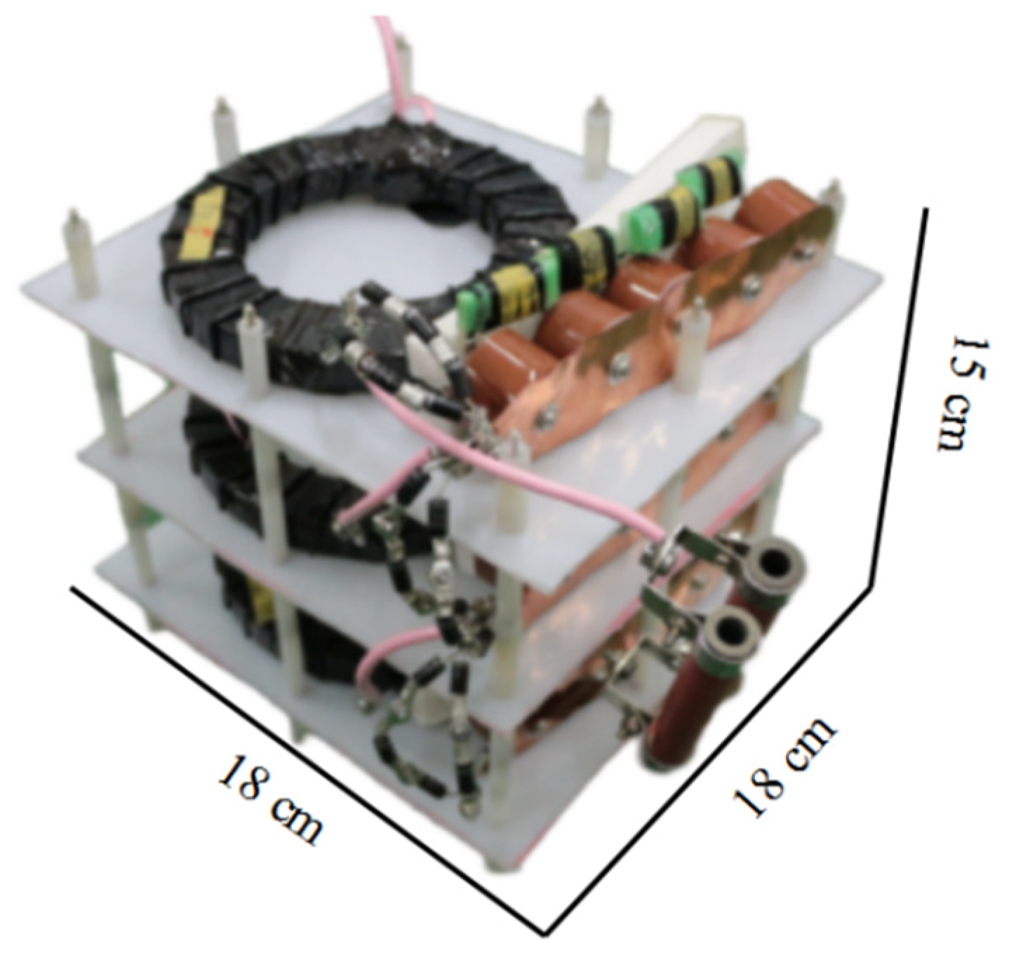
Figure 16 illustrates the physical configuration of the PFN generator, which comprises three modules based on the SPT design. The generator’s dimensions are 15 cm in length, 15 cm in width, and 12 cm in height. For insulation purposes, the primary coil of the SPT is separated from the magnetic core by a 1 cm-thick PC material. The three secondary circuits share a common primary charging circuit; consequently, the primary capacitance increases proportionally from 0.6 μF for a single module to 1.20 μF for two modules and 1.80 μF for three modules.
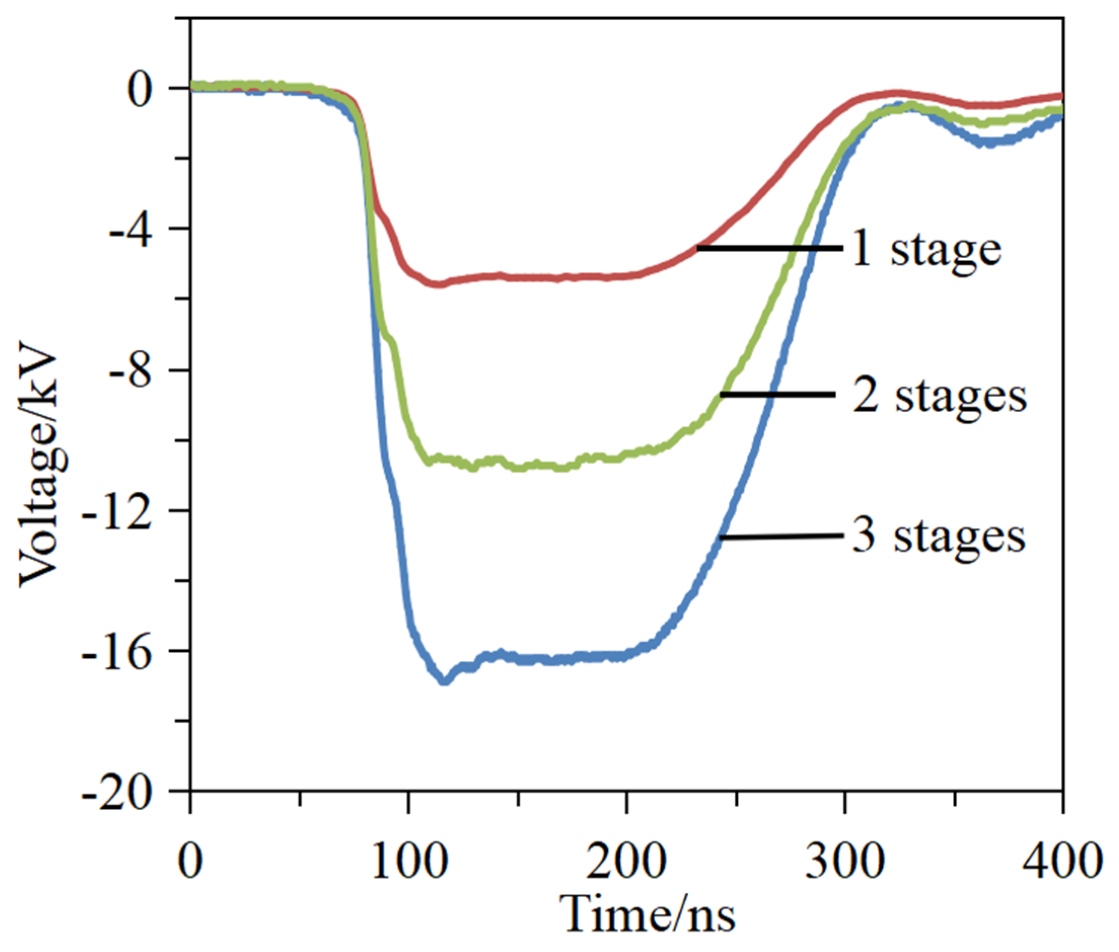
Figure 17 shows the output voltage waveforms of the PFN generators for modules 1, 2, and 3, each connected to loads of 27 Ω, 53 Ω, and 80 Ω, respectively, under a charging voltage of 950 V. The generators for modules 1 through 3 produce pulses with a half-width of 180 ns and peak voltages of −5.67 kV, −11.15 kV, and −16.9 kV, respectively, all exhibiting an identical front-edge duration of 19 ns. These results demonstrate that the pulse generator effectively achieves voltage multiplication through module superposition, without any increase in the rise and fall times of the output pulse as additional modules are combined.
The pulse generator delivers a high-output voltage within a single module and can achieve voltage doubling by stacking multiple modules, thereby increasing the voltage conversion ratio of the saturable pulse transformer (SPT). The saturation inductance of the SPT acts as a component of the LC circuit within the pulse-forming network (PFN) and incorporates pulse front edge-sharpening technology. This approach produces output pulses with shortened rise times that remain consistent regardless of the number of modules used. The SPT serves a dual function: it not only enables voltage amplification through transformer action but also regulates discharge via magnetic switching, contributing to a more compact overall design. Additionally, the primary charging circuits across all modules are controlled by a single semiconductor switch, simplifying the pulse generator’s architecture, reducing the number of switching elements, lowering manufacturing costs, and enhancing operational control.
A pulse generator comprising three pulse-forming network (PFN) modules, utilizing a saturable pulse transformer and a fast-recovery diode, was evaluated at a repetition rate of 20 kHz.
Figure 18 illustrates the output voltage waveform observed during burst mode operation. Each pulse train consists of 10 pulses, during which the primary capacitor C
0 is incrementally charged by these pulses. Due to the limitations of the DC power supply, the voltage across the primary capacitor C
0 decreases over time, causing a slight reduction in the pulse generator’s output voltage. To achieve a more stable output voltage and increase the number of pulses within each pulse train, it is advisable to use either a high-power, high-voltage DC power supply or a capacitor with a larger capacitance for pulse charging. In the current experimental setup, the maximum achievable frequency is limited by the switching frequency of the primary semiconductor device.
5. Conclusions
This study presents an all-solid-state pulse-forming network (PFN) pulse generator that employs SPT and fast recovery diodes. The SPT serves a dual function: it acts as a transformer to boost voltage and operates as a closing switch to regulate discharge on the secondary side. Additionally, the secondary inductance of the SPT is integrated as the inductive component of the initial LC stage within the PFN. Multiple modules share a common primary charging circuit, ensuring synchronized charging across the system. Furthermore, the reverse recovery characteristic of the fast recovery diode is exploited to sharpen the front edge of the pulse, enabling the generation of high-voltage pulses with a rise time below 20 ns when applied to low-resistance loads. The device successfully produced pulses with a voltage amplitude of –16.9 kV, a rise time of 19 ns, a half-height pulse width of 180 ns, and a repetition rate of 20 kHz. The compact three-module PFN pulse generator measures only 15 cm in length, 15 cm in width, and 12 cm in height.
The pulse generator utilizes a pulse-forming network (PFN) at its input, which restricts flexibility in adjusting both the pulse width and the output load. As a result, a quasi-square pulse can only be achieved under matched impedance conditions. Voltage multiplication in this pulse generator can be accomplished either by superimposing multiple modules or by increasing the transformation ratio of the SPT, without a corresponding increase in pulse rise time. The device features a compact structure, low cost, high efficiency, ease of control, modular design, short pulse rise time, and the ability to generate near-square wave pulses. These characteristics make it particularly well-suited for producing high-voltage, high-frequency, narrow pulses with rapid rise times in load impedances on the order of tens of ohms, such as those required for atrial fibrillation ablation applications.
