Abstract
Low-voltage power converters in the 25–200 V range are increasingly employed in emerging applications such as hybrid electric vehicles (HEVs), photovoltaic systems with battery storage, and electric propulsion systems for recreational boats. In these contexts, 48 V battery systems have become standard, due to safety considerations. Among various converter topologies, H-bridge configurations operating around 100 V DC are widely used in laboratory-scale prototyping. While MOSFETs are the preferred switching devices in this voltage range, due to their high efficiency and fast switching characteristics, they also introduce design challenges related to high current slew rates and associated overvoltage spikes caused by parasitic inductances in the PCB layout. These overvoltages, though modest in absolute terms, can be critical in low-voltage systems, due to the lower device ratings. This paper presents design strategies and layout best practice for a 120 V, 50 A H-bridge converter using 200 V rated MOSFETs. The effectiveness of various mitigation techniques—including the use of ceramic capacitors in parallel with film and electrolytic types, Schottky diodes across MOSFETs, and snubber circuits—is evaluated and experimentally validated on a dedicated prototype. The results highlight the critical role of PCB design in ensuring switching reliability and device protection in low-voltage converter systems. In addition, with the design solutions shown in this study, it was possible to obtain a voltage overshoot during switching of just 165 V with a 120 V DC-link voltage, which guarantees a sufficient safety margin for the MOSFET rated voltage.
1. Introduction
Hybrid electric vehicles (HEVs) have had increasing attention in recent years, since they allow a significant reduction in fuel consumption and can be seen as a winning solution for moving smoothly from traditional vehicles to electric vehicles (EVs) [1,2]. HEVs, which rely on electric motors powered by battery systems and power electronic converters, represent a key technology in the global effort to reduce greenhouse gas emissions and improve energy efficiency in the transportation sector [3]. As a matter of fact, since HEVs have a smaller battery compared to EVs, if one considers the worldwide lifetime emissions (i.e., fuel emissions, electricity emissions, and battery production emissions), HEV and Plug-in HEV (PHEV) can have lower worldwide lifetime emissions, as demonstrated in [4]. The overall life cycle is also analyzed in [5], where both fuel economy and battery health are taken into account.
For the optimization of HEV, different aspects should be taken into account. Several studies focus on the energy management system (EMS) of a specific architecture [1,2], whereas other studies analyze different architectures. In particular, in [6], the fuel economies of parallel and series-parallel architecture are compared, whereas [7] analyses the fuel economy benefits of the introduction of an additional clutch in a series-parallel architecture. Moreover, engine and electric motor sizing also play a crucial role in HEV performance, as highlighted in [8].
Besides EMS and architecture optimization, electrical component performance highly affects HEV efficiency. As a matter of fact, as highlighted in [9], the electrical component efficiency not only affects the HEV efficiency, but can also drive the choice of a specific hybrid architecture, among others. Moreover, electrical component efficiency depends on driving conditions, as analyzed in [10]. For that reason, several studies analyze electric motors for electric vehicles, focusing both on the study of less-rare-earth permanent magnet machines [11], on motor noise reduction [12], and on efficiency increase in high-speed motors [13]. Together with electric motors, one of the most significant components of HEVs is the storage system. In this regard, a series HEV based only on supercapacitor storage was analyzed in [14], with a particular focus on storage sizing. On the other hand, an HEV with a hybrid energy storage system (HESS) based on the combined use of battery and supercapacitors was analyzed in [15]. When HESSs are used, multiport converters are a winning solution to optimize efficiency and cost. Regarding this aspect, a multiport inverter with two inputs on the DC-side is analyzed in [16], where a battery and a supercapacitor are managed separately by the inverter. Regarding multiport DC-DC converters, a double input DC-DC converter is shown in [17], and a fast control for such a converter is proposed in [18].
For all these motivations, power electronic converter design is a topic of great interest for HEVs. Moreover, such converters are also a key technology in several other applications.
Low-voltage (approximately 25 V to 200 V) power electronic converters with power ratings in the kilowatt range are gaining increasing attention for several emerging applications, including renewable energy sources (RES) [19] and electric recreational boats [20]. In particular, converters operating within this voltage and power range are commonly employed to interconnect photovoltaic (PV) [21,22] with a common DC-bus in grid-connected systems, or to connect them with battery storage in small islanded microgrids, such as those supplying remote buildings or mountain huts [23,24]. Similarly, in the automotive sector, low-voltage converters are widely adopted in mild-hybrid electric vehicles to interface 48 V battery systems with electric motors [25,26]. A comparable use case is found in electric propulsion systems for small recreational boats, where 48 V battery packs are often used to supply the main drive motor. The widespread adoption of 48 V as a standard in these applications is primarily driven by safety considerations.
In laboratory environments, particularly when developing and testing small-scale prototypes of multilevel converters, an H-bridge configuration operating around 100 V DC is often chosen as a practical and safe compromise [27]. At these voltage levels, MOSFETs are typically the preferred switching devices, due to their high switching speed and efficiency [28,29], with a great interest in the last years on wide band-gap devices [30]. However, the use of MOSFETs introduces specific challenges for the design of the printed circuit board (PCB).
One of the main issues arises from the very high current slew rate (di/dt) associated with fast MOSFET switching. High di/dt values exacerbate the effects of parasitic inductances inherent in PCB layouts, leading to significant overvoltage spikes during switching transitions. This phenomenon becomes particularly critical in low-voltage converters, where the relative impact of these overvoltages is more pronounced compared to high-voltage systems. For example, an overvoltage spike of 100 V may be tolerable in a converter employing 1200 V IGBTs and operating at 800 V DC (resulting in a transient up to 900 V), but the same overvoltage in a 200 V rated MOSFET system operating at 120 V DC would lead to a transient of 220 V, which could exceed the device’s maximum ratings and result in failure.
It is important to note that the magnitude of overvoltage spikes is primarily influenced by the rate of current change and by parasitic inductances, rather than by the nominal voltage of the switching devices. As a result, even though absolute overvoltages may be similar in both low-voltage MOSFET-based and high-voltage IGBT-based converters, their relative severity is substantially higher in the former, due to the lower voltage rating of the components. Consequently, the PCB layout design for low-voltage converters using MOSFETs is particularly critical and often more complex than that required for high-voltage IGBT converters with comparable current ratings. Careful minimization of parasitic inductances and optimized routing are therefore essential to ensure reliable operation and to prevent device overstress during switching events.
PCB design for power converters is a topic of great interest in the technical literature, and several papers investigate this topic. The first aspect that should be taken into account when designing a power converter is the PCB layout itself. In [31], the MOSFET parasitics and the PCB parasitic inductances are evaluated as a function of temperature variation, whereas [32] analyzes the parasitic inductance connected to the different PCB layout in detail. In particular, the traces between the DC-link capacitor and the MOSFET pins should be particularly short, in order to reduce the parasitic inductance; moreover, through-hole film capacitors are characterized by a relatively high parasitic inductance. For these reasons, a SMD ceramic capacitor is usually located close to the MOSFET pin. Even if this capacitor is electrically connected in parallel to the main DC-link capacitor, the aim of this component is to reduce the overvoltage during the switching; for this reason, it is often called the DC-side snubber. In order to clearly identify this component, in this paper, we will refer to it as the DC-side capacitor. In [33], the connection of the DC-side capacitor is evaluated in order to reduce the parasitic inductance. The DC-side capacitor sizing effect is analyzed in [34,35]. Besides the possibility to use DC-side capacitors, RC snubbers were investigated in [36,37], in parallel to the single MOSFET (instead of being in parallel to the entire leg as for the DC-side capacitor).
While previous studies have provided detailed analyses of individual design aspects—such as PCB layout, DC-link capacitor placement, or snubber circuits—their scope has typically been limited to isolated countermeasures. In contrast, this work presents a comprehensive experimental evaluation of multiple voltage spike mitigation strategies applied to the same hardware platform. By systematically assessing each countermeasure under identical test conditions, this study offers a unique comparative insight into their relative effectiveness and interactions. The proposed approach reflects the holistic nature of power converter design, where performance optimization cannot rely on a single solution, but rather on the coordinated application of multiple techniques. As such, this work aims to serve not only as an experimental benchmark but also as a practical design guide for engineers facing similar challenges. The main differences between the works in the technical literature and this paper are summarized in Table 1.

Table 1.
Literature review on PCB design for low-voltage power converters. Table shows which aspects are analyzed in the different papers.
2. PCB Design
2.1. Converter Structure
The analyzed converter is a standard H-bridge with 4 MOSFETs and it is shown below in Figure 1.
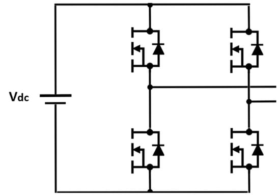
Figure 1.
H-bridge architecture.
The MOSFETs used in the prototype are the 200 V-88 A (IPP110N20N3G). Since in any condition, the rated voltage of the device must not be exceeded, an appropriate margin should be considered, as it is normal that during switching, a certain overvoltage occurs in the device. For this reason, the rated voltage of the converter is fixed to 120 V. Please note that this value is fixed arbitrarily by the designer. However, 120 V for a 200 V MOSFET is considered good practice, as will also be demonstrated by the experimental tests. Regarding the current level, considering that the thermal constant of the devices is very small (typically a few milliseconds), it is appropriate to include a certain margin, even on the current level. For this reason, the rated current of the device was chosen to be 50 A. This is the current at which the test on the prototype will be carried out. The main converter parameters are reported in Table 2, whereas the 3D design of the overall PCB is shown in Figure 2.

Table 2.
Converter parameters.
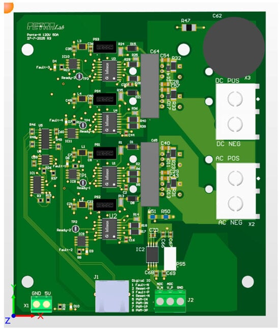
Figure 2.
PCB design.
An enlargement of one of the two legs is shown in Figure 3, viewed from the top side and the bottom side. Since the two legs are identical from a design point of view, all analyses will be carried out for a single leg, with the assumption that the same conclusions derived from this study can be extended to the full converter (H-bridge, i.e., two legs) or to a three-phase inverter (i.e., three legs).
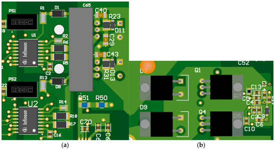
Figure 3.
Enlargement of one of the two legs of the converter. (a) Top. (b) Bottom.
As can be seen from Figure 2, the PCB is equipped with additional components for signal processing. As a matter of fact, the PCB receives a differential signal for each leg and the dead times are imposed by the PCB with an analog circuit. Moreover, faults and reset signals are also sent to and from the PCB, using differential signals. The part of the circuit regarding signal processing from differential signals to single-ended signals, the dead time circuit and the DC-voltage measurement circuit, are not analyzed in this paper. Indeed, even if they are fundamental for the operation of the PCB, they are outside the focus of this study.
2.2. Isolated Gate Unit Supply
In order to drive the MOSFET, an isolated supply should be provided for each device. In the proposed design, it was chosen to supply the gate of the MOSFET at +17 V for turn-on and at −7 V (with respect to the source of the device) for turn-off.
The isolated gate unit in Figure 4 is based on the isolated DC-DC converter ROE-0524 by RECOM. The ROE-0524 manufacturer does not recommend specific capacitor values for that specific DC-DC converter; however, it recommends a 10 μF capacitor on the input side of the ROE-0505 [38]. Since ROE-0524 and ROE-0505 have the same rated input current, it was chosen to use the same input capacitance. Since in the proposed converter a CLC configuration is used on the input side, two 4.7 μF capacitors were chosen so that the sum of the two capacitors is about the capacitance value suggested by RECOM. Regarding the output capacitor, since the output current is approximately 5/24 of the input current, the output capacitor was scaled based on the current value, and a 1 μF capacitor was chosen. Since a +17 V and −7 voltage supply with respect to the MOSFET source are necessary, a voltage divider is implemented, exploiting a 7 V Zener. Two couples of 1 μF and 4.7 μF capacitors are connected in parallel. The parallel connection of capacitors with different capacitance values is a standard practice to reduce the equivalent parasitic resistance.

Figure 4.
Gate isolated supply based on a 5 V to 24 V DC-DC converter and on a 7 V diode.
2.3. Parasitic Inductance
One of the main PCB design challenges is to reduce the parasitic inductance between the DC-link capacitor and the power switch device (e.g., MOSFET in the considered layout). During the switching process, even if the output current remains almost constant, it reverses direction in the DC-link capacitor. Especially with MOSFETs, the commutation is very fast, since the turn-on and turn-off times are about 50 ns, but the time during which almost all of the current transitions from one device to the other occur can last about 5 ns. As can be noticed by observing Figure 5, if the parasitic inductance between capacitor and device is significant, high overvoltage can occur. As an example, if the converter is working with the rated current of 50 A (therefore, a Δi = 50 A), a parasitic inductance of just 20 nH can cause an overvoltage during switching of up to 100 V, as shown in Equation (1), where VDSsurge−VDC is the overvoltage caused by parasitic inductance, Lpar is the parasitic inductance, Δi is the current variation during switching, and Δt is the switching duration. Please note that if a 100 V overvoltage occurs when the converter is supplied with the rated voltage of 120 V, the total voltage on the device is 220 V and the device will fail.
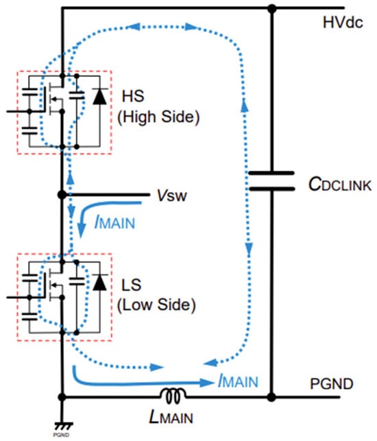
Figure 5.
Parasitic inductance and current path before and after switching [39].
To evaluate the impact of different designs on the parasitic inductance (Lmain in Figure 5), it is useful to define the formula for elementary geometries. For a cylindrical conductor, the stray inductance can be approximated by the formula in Equation (2) [40]. This formula can be used to estimate the parasitic inductance of the connector leads of through-hole components (e.g., through-hole film capacitors).
where is the wire length and is the wire radius.
Regarding the parasitic inductance of a PCB trace, it can be approximated by Equation (3) [41].
where is the trace length, is the thickness of the dielectric between the trace and the ground plane, and is the trace width.
From Equation (3), it is possible to note that the greater the width of the trace, the lower the inductance. Considering a 1 mm dielectric thickness (inductance between an inner trace and an inner ground plane) for a 0.5 mm trace, the parasitic inductance is about 4 nH/cm, whereas for a 10 mm trace, the inductance is about 0.4 nH/cm. It is worth noting that, for this reason, parasitic inductance is further reduced if copper planes are used instead of traces.
Note that it is also important to minimize the area formed between the gate resistor and the gate itself, to minimize the parasitic inductance at the input of the MOS.
2.4. PCB Layers and Copper Planes
In the current project, it was decided to design a four-layer PCB. The main reason for this choice is to use the two inner layers for DC+ and DC− (i.e., the two DC voltage power connections of the converter) and to keep the external layers for AC connections. The use of copper planes instead of thin traces reduces the stray inductance, and therefore the overvoltage, during switching caused by high di/dt.
The DC+ and DC− planes can be clearly seen in the inner layers in Figure 6, whereas the two AC connections (AC+ and AC−) are highlighted in Figure 7, where the top and bottom layers are reported. The AC connections are present in both the top and bottom layers to reduce the current flow in each layer and thus prevent overheating of the PCB. Please note that even though they are called AC+ and AC−, the converter can also operate as a DC-DC (i.e., the AC+ and AC− are the connections of the converter port, where the current can be either DC or AC).
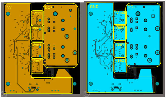
Figure 6.
PCB inner layers.
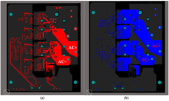
Figure 7.
PCB layers. (a) Top. (b) Bottom.
2.5. Snubber Design
An effective way to counteract voltage spikes during switching is to introduce a capacitor snubber, as shown in Figure 8 [39].
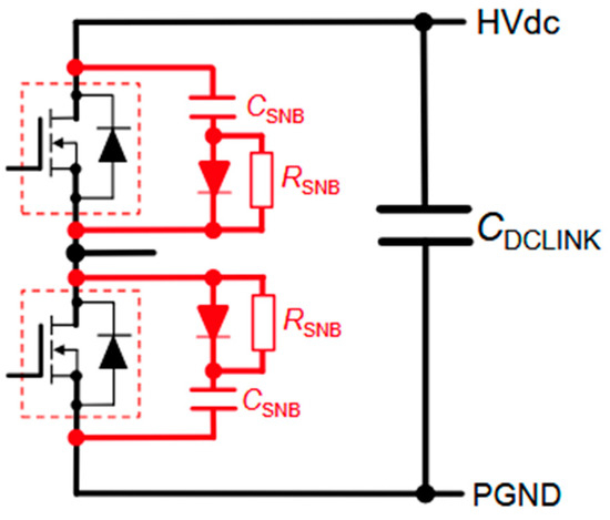
Figure 8.
Snubber circuit.
In particular, a passive snubber circuit has been selected, in which a capacitor, a resistor, and a diode are employed. Fast MOSFET switching in the 50 A, 120 V H-bridge creates rapid current changes (high di/dt), which interact with the parasitic inductance in PCB traces, causing resonant ringing with the MOSFET’s parasitic output capacitance. The result is overvoltage spikes that may exceed device ratings. The snubber addresses this by adding a capacitor CSNB and resistor RSNB in series with a diode, creating a discharge path that activates when the voltage spike occurs.
Out of the four snubber circuit variants analyzed in [39], the discharging RCD variant has been selected for this design due to its superior ability to absorb surge energy while minimizing continuous losses. Specifically, during the MOSFET turn-off, the diode directs the spike into Csn, reducing the voltage oscillations, while during turn-on, the resistor RSNB dissipates the stored energy, which is controlled by design to avoid excess heating. This topology offers a better surge-clamping performance than a simple RC snubber, and fewer losses than a non-discharge version, while maintaining simpler PCB layout requirements than more complex active snubbers. The snubber capacitor Csn should be designed based on electrostatic capacity derived from Equation (4) [39], where VDSsurge is defined as the maximum surge of VDS, Vdc is the DC-side voltage (DC+/DC−), and Imain is the converter rated current.
Please note that Lmain is calculated from the observed ringing frequency with Equation (5) [39],
where Coss is the output parasitic capacitance of the MOSFET (135 pF, as specified in the Infineon datasheet) and fring is the frequency of voltage oscillations during switching.
The resulting Lmain value derived from Equation (5) [39] is 117 nH. The snubber resistor must be selected, considering Equation (6) [42].
2.6. Conduction Losses, Switching Losses, and Snubber Losses
The introduction of the snubber circuit ensures a great reduction in voltage overshoot during switching. However, the snubber circuit is associated with additional losses, since the snubber capacitor is charged and discharged every switching period and the energy is dissipated in the snubber resistor during the discharging phase. To evaluate the impact of these losses, it is useful to estimate the snubber losses and to compare them with the conduction losses and the switching losses.
To estimate the losses of a single leg of the converter, a functioning in buck converter mode at a rated voltage and current (i.e., 120 V, 50 A) with a 50% duty cycle can be considered. The conduction losses will be the sum of the conduction losses of both MOSFETs and can be evaluated as in Equation (7) [43].
where Ron is the on-state resistance of the MOSFET and Id is the drain current, which corresponds to the output current of the converter if one neglects the switching phase. Please note that since the duty cycle is 50%, the average conduction losses of each device are half of the value calculated in (7), which corresponds to the sum of the average conduction losses of both devices.
Regarding the switching losses, the datasheet of IPP110N20N3G provides 44 ns as turn-on time and 52 ns as turn-off time, evaluated for Vgs = 10 V and Rg = 1.6 Ω., where Vgs and Rg are the gate driver on-voltage and the gate driver resistance, respectively. According to [43], turn-on and turn-off time can be considered to be inversely proportional to the gate drive current. In this work, Vgs = 17 V and Rg = 5.5 Ω; therefore, the gate current is about half of the corresponding gate current of the datasheet. For this reason, a reasonable approximation is given by Equation (8) and according to [43], the switching losses at 30 kHz can be evaluated as in Equation (9).
where VDC is the DC-link voltage and fsw is the switching frequency. Please note that the switching losses of Equation (9) are related to the upper MOSFET of the leg; for the lower device of the leg, the diode is involved during the switching phase and the reverse recovery losses are significantly lower than the switching losses of the MOSFET.
Regarding the snubber losses, both snubber capacitors of the upper and lower MOSFETs have to charge and discharge each switching cycle. The losses of a single snubber can be evaluated according to [36], as in Equation (10).
The value of voltage overshoot VDSsurge can be evaluated from the experimental result in the final configuration. Considering that the snubber losses are equal for both upper and lower MOSFET, the total losses related to the snubbers will therefore be 1.8 W.
The converter losses are summarized in Table 3. Since the two legs of the H-bridge are identical, the evaluation is carried out on a single leg, considering a DC-DC operation. It is worth noting that the snubber losses are about 10% of the switching losses and therefore, the introduction of such a countermeasure to reduce voltage overshoot is highly effective.

Table 3.
Losses of a single leg in buck-mode with 50% duty cycle, Vdc = 120 V, Id = 50 A, fsw = 30 kHz.
3. Experimental Validation
In this chapter, experimental validation is shown. In Section 3.1, the double pulse test is described, which is used to evaluate the voltage overshoot during switching at the rated current. Then, the test bench is presented in Section 3.2, showing both the test bench scheme and the image of the experimental setup. Finally, the experimental results are shown in Section 3.3
3.1. Double Pulse Test
Since the aim of the experimental tests is to evaluate the voltage overshoot during switching, a standard double pulse test procedure was carried out, with the aim of measuring the drain-source voltages during switching.
During the test, the leg is connected to an R-L load (i.e., the load is connected between DC− and the leg middle point, AC+ or AC−). The load values on the test bench are 1 Ω and 100 μH, approximately.
In the “OFF” state, the lower switch is closed, and the load is short circuited; therefore, the current decreases until it reaches zero. When the upper switch is closed (“ON” state), the current starts to increase.
First, a pulse (“ON” state) is applied to reach the rated current (i.e., 50 A) with a fixed voltage; subsequently, a 10 μs “OFF” period is applied, during which the current remains almost constant, since the R value is quite low. Finally, a second pulse of 4 μs is applied. In this way, turn-on and turn-off of both switches at the rated current are performed.
Since the rated voltage of the devices is 200 V, the tests are carried out, starting from a low voltage supply and gradually increasing the value in order to avoid MOSFET failure. Moreover, the PCB was manufactured by a dedicated company, but the components were soldered in the laboratory of the University of Genova. In this way, it was possible to conduct tests on the board by adding components one by one, and therefore analyzing the effect of each individual countermeasure to reduce the overvoltage during switching.
All the tests were conducted on one leg; however, the design of the two legs is identical. In particular, each leg has its own film capacitor and SMD capacitor, which are as close as possible to the MOSFETs. For this reason, the results obtained can be extended to the other leg, and the same leg design can be copied to design a three-phase system.
3.2. Test Bench
The scheme of the test bench is shown in Figure 9, where the load is shown as an inductor. The quantities measured during the tests are the VDS of both switches and the output current, as schematized in Figure 9.
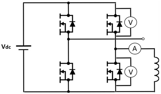
Figure 9.
Test bench scheme.
The experimental setup is shown in Figure 10. A dSpace MicroLabBox is used to control the converter. The voltages are measured with Pico Technology TA043 differential probes with 100 MHz bandwidth, directly on the MOSFET pin, in order to correctly measure the voltage on the MOSFET. The output current is measured with a 50 A peak current LeCroy CP030 current probe with 50 MHz bandwidth. The oscilloscope is a 12-bit 500 MHz LeCroy MDA-805 A.
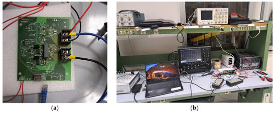
Figure 10.
Test bench. (a) PCB. (b) Complete test bench.
A power supply is used to charge the DC-link capacitors. The connection between dSpace and the PCB is made with an RJ45 cable. Please note that only the components of one leg are soldered; in fact, the tests are carried out on only one leg, since the design of the two legs is identical.
3.3. Experimental Results
The design without any counteraction for overvoltage limitation is taken as the benchmark to evaluate the benefits of the different solutions that will be implemented, one by one. Subsequently, the results obtained with the following four improvements will be analyzed:
- First improvement: addition of a 250 V-40 A Schottky diode in parallel to each MOSFET.
- Second improvement: addition of a 0.1 uF SMD ceramic capacitor on the DC-side.
- Third improvement: addition of a 2.2 nF-5.1 Ω snubber.
- Fourth improvement: addition of a diode in parallel to snubber resistor.
Each improvement will be added to the previous one, in order to evaluate the effectiveness of each countermeasure and finally arrive at a definitive converter layout. At the end of the experimental results, Table 4 will summarize the voltage overshoot obtained in the different configurations.

Table 4.
Comparison of different PCB configurations.
Even if the design using copper planes shown in Figure 6 minimizes the stray inductance, the first test was carried out without any counteraction for overvoltage suppression. Regarding the DC-link capacitor, in this configuration, only the 4.7 μF through-hole film capacitor is mounted.
The double pulse test results are shown in Figure 11, and an enlargement is reported in Figure 12. One can note that the turn-off is without overvoltage, whereas the overvoltage occurs during turn-on, and the effect is higher when the current is higher. From the enlargement, despite a DC-voltage of only 80 V and a current of only 25 A, the Vds voltage on the lower switch reaches 199 V (please note that the overvoltage peak was evaluated with the cursor of the oscilloscope). This behavior is clearly unacceptable, and counteractions are needed.
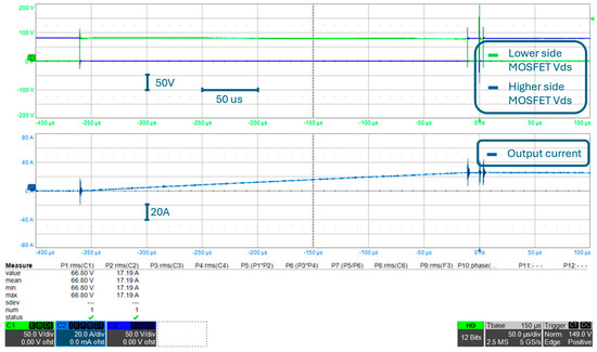
Figure 11.
Reference case, Vdc 80 V, Id = 25 A.
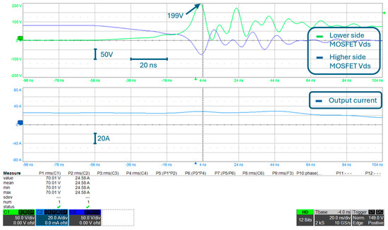
Figure 12.
Reference case (zoom), Vdc 80 V, Id = 25 A.
Since the overshoot is already close to the MOSFET rated voltage (i.e., 200 V), increasing the current would lead to MOSFET failure. For this reason, the converter leg was not tested at the rated current of 50 A. In the next paragraph, the test will be shown for a current of 50 A, and a reduction in the voltage overshoot will be shown. It is worth noting that for a fair comparison, the test should be carried out at the same current, since the voltage overshoot depends on the rate of current change. However, conducting the reference test at 25 A is a conservative approach, since the benefit derived from the introduction of the diodes in parallel to the MOSFET would be even more evident if both tests were conducted at the same current.
The first improvement that was tested was the addition of a 250 V-40 A Schottky diode in parallel to each MOSFET. The turn-on of the diode is faster than the turn-on of the MOSFET body diode, and therefore, the overvoltage during switching can be reduced to 188 V, even with the output current increased to the rated value (i.e., 50 A), as can be seen in Figure 13 and Figure 14.
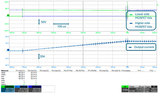
Figure 13.
First improvement: addition of a 250 V-40 A Schottky diode in parallel to each MOSFET. Vdc = 80 V, Id = 50 A.
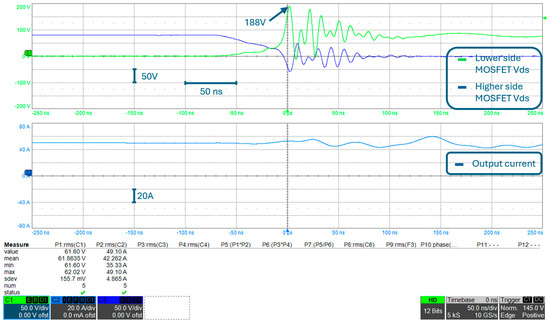
Figure 14.
First improvement (zoom): addition of a 250 V-40 A Schottky diode in parallel to each MOSFET. Vdc = 80 V, Id = 50 A.
The second counteraction was the addition of a 0.1 μF ceramic SMD capacitor in parallel to the DC-link film capacitor (C29 in Figure 15a). Indeed, film capacitors have a significant parasitic inductance, compared to SMD ceramic capacitors. As can be noticed from Figure 15b, the leads of the capacitor are two cylindrical conductors of about 1.5 cm each; therefore, a 15 nH parasitic inductance can be estimated just in lead connectors.
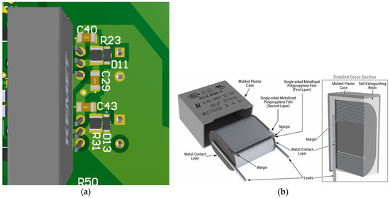
Figure 15.
(a) Addition of DC-link 0.1 uF ceramic SMD capacitor. (b) Constructive detail of film capacitor.
The benefits obtained with the introduction of C29 are shown in Figure 16 and Figure 17, where the same double pulse test is carried out. Despite the increase in the DC-link voltage from 80 V to 100 V, the same overvoltage during switching is observed as in the previous case study.
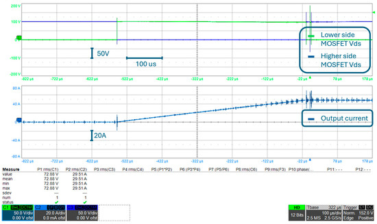
Figure 16.
Second improvement: Addition of 0.1 uF SMD ceramic capacitor on the DC-side. Vdc = 100 V, Id = 50 A.
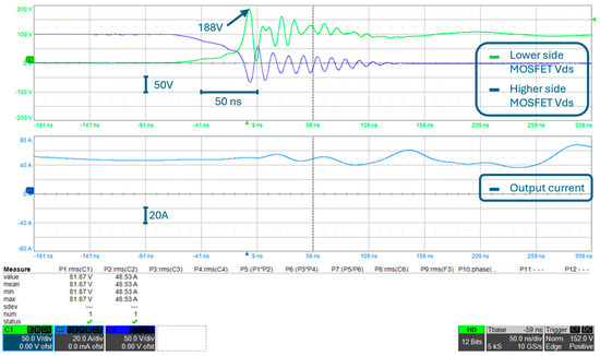
Figure 17.
Second improvement (zoom): addition of 0.1 uF SMD ceramic capacitor on the DC-side. Vdc = 100 V, Id = 50 A.
According to the theory presented in Section 2, a 2.2 nF-5.1 Ω snubber was soldered in parallel to the MOSFET (C40 and R23 in Figure 15a). The benefits of introducing the snubber are evident in Figure 18 and Figure 19, where the voltage overshoot at 100 Vdc is reduced from 188 V in the previous configuration to 173 V in the current configuration. Please note that Equation (4) has been used to calculate the snubber capacitor value, where 188 V and 100 V have been considered as VDSsurge and VHVdc, respectively. Please note that the snubber tuning is comparable to the one shown in [37], where optimal performance was obtained for a 1 nF-5 Ω snubber, obtaining analogous benefits.
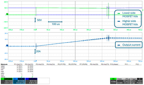
Figure 18.
Third improvement: addition of 2.2 nF-5.1 Ω snubber. Vdc = 100 V, Id = 50 A.
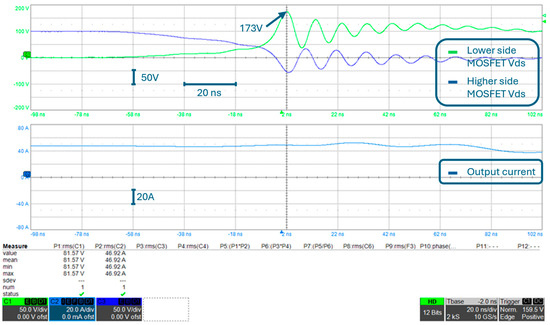
Figure 19.
Third improvement (zoom): addition of 2.2 nF-5.1 Ω snubber. Vdc = 100 V, Id = 50 A.
In the current configuration, a test at 120 V was also carried out. The measured overvoltage during switching reached 195 V, as can be noticed from Figure 20 and Figure 21. Since the overvoltage is very close to the device voltage limit of 200 V, an additional countermeasure is required.
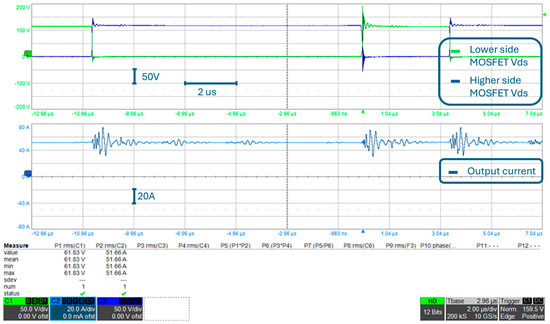
Figure 20.
Third improvement: addition of 2.2 nF-5.1 Ω snubber. Vdc = 120 V, Id = 50 A.
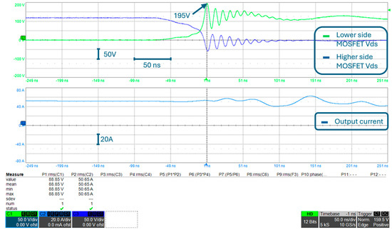
Figure 21.
Third improvement (zoom): addition of 2.2 nF-5.1 Ω snubber. Vdc = 120 V, Id = 50 A.
To keep the voltage across the device within safe operating limits, a diode was soldered in parallel to the snubber resistor (D11 in Figure 15a). The diode short-circuits the snubber resistor during snubber capacitor charging (i.e., during device turn-off), thereby avoiding losses from the snubber resistor. The diode is not only beneficial from an efficiency point of view. In fact, the possibility of faster charging of the snubber capacitor allows a significant reduction in the voltage spike from 195 V to 165 V, as can be seen in Figure 22 and Figure 23.
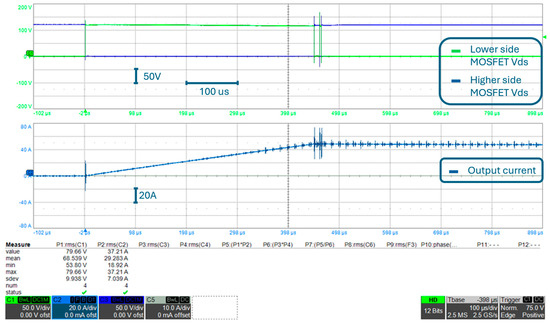
Figure 22.
Fourth improvement: addition of diode in parallel to snubber resistor. Vdc = 120 V, Id = 50 A.
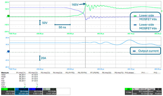
Figure 23.
Fourth improvement (zoom): addition of diode in parallel to snubber resistor. Vdc = 120 V, Id = 50 A.
Considering that this is the final configuration of the converter, converter output voltage (i.e., the voltage between AC+ and DC−) and the converter output current are reported in Figure 24, which are measured during the double pulse test shown in Figure 22 and Figure 23. Please note that the converter output current shown in Figure 24 is measured at the same point of the circuit as the output current shown in other experimental results, according to what is shown in Figure 9. The output voltage is measured at the converter output connection and is approximately the same waveform as the lower side MOSFET VDS. As a matter of fact, if one observes Figure 9, it can be noted that, neglecting PCB parasitic inductances, converter output voltage corresponds to lower-side MOSFET VDS. Moreover, please note that, as described in Section 3.1, the double pulse test consists of an initial “pulse” (with an approximate time duration of 440 μs in this test) of the output voltage, during which the current rises to the rated value, followed by a 10 μs interval where the output voltage is zero, and a second “pulse” of 4 μs is used to evaluate the overvoltage on the device during switching at the rated current, both at turn-on and turn-off. The entire double pulse test is therefore shown in Figure 24.
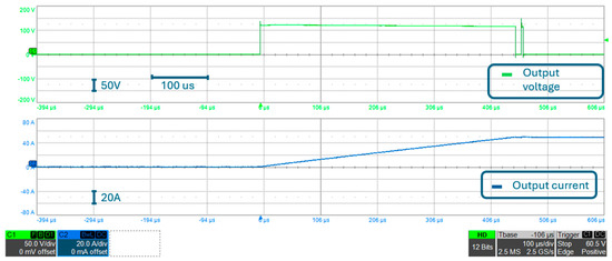
Figure 24.
Fourth improvement. Converter output voltage and output current.
3.4. Synthesis of Experimental Results
The main results obtained in the previous subsections are summarized in Table 4, where the overvoltage in the MOSFETs, obtained with different configurations, PCB configurations, and for different supply voltage, are reported.
As mentioned in Section 3.3, the MOSFET rated voltage is 200 V and a voltage transient during switching above this value will lead to device failure. The tests are carried out with increasing DC input voltage and increasing output current, and are stopped when the overvoltage approaches the rated voltage, in order to prevent device failure. Countermeasures to reduce voltage overshoot were soldered onto the PCB one at a time, to verify the effectiveness of each solution individually.
Double pulse was performed at first on the reference case, i.e., the PCB, without any countermeasure for overvoltage reduction. With a reduced DC input voltage (80 V), tests were carried out with increasing output current. The test was stopped at 25 A, since voltage during switching almost reached the MOSFET rated voltage. Subsequently, 250 V-40 A Schottky diodes were soldered in parallel to each MOSFET. In this configuration, it was possible to increase the current to the rated value (50 A) with a reduced overvoltage of 188 V. After that, a 0.1 μF SMD ceramic capacitor was soldered significantly close to the MOSFET pin. Please note that from an electrical point of view, this capacitor is in parallel to the DC-input capacitor. In this configuration, it was possible to reach 100 V of input voltage, obtaining the same overvoltage of 188 V. Further to this, a 1 nF-5.1 Ω RC snubber was added in parallel to each MOSFET; in this configuration, it was possible to reach the converter rated value (i.e., 120 V of input voltage and 50 A of output current), keeping the overvoltage below MOSFET rated voltage. However, the overvoltage in this configuration (i.e., 195 V), was close to the MOSFET rated voltage and, therefore, an additional diode was soldered in parallel to the snubber resistor. In this last configuration, the overvoltage peak during switching was only 165 V, which allows us to have a significant margin with respect to the device’s rated voltage.
3.5. Switching and Snubber Losses Measurement
In order to validate the estimated switching and snubber losses experimentally, the converter output was connected directly to the inductor (i.e., removing the 1 Ω resistance). In this way, it was possible to supply the inductor with the rated current (50 A) at a very low duty cycle (1.25%), obtaining a very low output power. Considering that both the switching losses and the snubber losses do not depend on the converter duty cycle, they are almost the same losses as if the converter was working at a 50% duty cycle, as hypothesized in Section 2.6. The input power of the converter was measured for this working point at 10 kHz, 20 kHz, 30 kHz, 40 kHz, and 50 kHz of switching frequency. Since conduction losses and converter output power are almost independent from switching frequency, the only difference in converter input power at different frequencies should be attributed to switching and snubber losses.
The results of the tests are reported in Table 5. Conduction losses, switching losses, and output power were evaluated with the following procedure. Firstly, converter input power was evaluated at different switching frequencies, always keeping a constant output current of 50 A. Since conduction losses and output power are dependent on the output current but not on switching frequency, the input power variation at different switching frequencies can be attributed uniquely to the switching losses and snubber losses. Considering the input variation between 10 kHz and 50 kHz of about 30 W, switching and snubber losses can be estimated at about 0.75 W/kHz. With the MOSFET on-resistance being about 11 mΩ, according to what is presented in Section 2.6, the conduction losses at 50 A can be estimated to be 27.5 W. Please note that the MOSFET on-resistance was measured experimentally, injecting a constant current of 50 A with a power supply while the MOSFET was in the on-state, confirming the value shown in the datasheet.

Table 5.
Converter input power vs. switching frequency (120 V DC-link, 50 A output current).
Considering the input power at 10 kHz, the output power can be estimated by subtracting conduction losses (27.5 A) and switching losses (7.5 W, with switching losses estimated to be 0.75 W/kHz). The corresponding output power of 54 W was considered to be the same for all the different switching frequencies, and switching losses were consequently updated for each switching frequency.
4. Conclusions
In this study, a 50 A-120 V H-bridge converter was developed. One of the main challenges in such a design is to reduce overvoltage peaks during switching, which could cause device faults. For this reason, several counteractions were implemented and tested, one by one. Starting from the reference case, fast Schottky diodes were soldered in parallel to the MOSFETs. Then, a 0.1 μF SMD ceramic capacitor was added in parallel to the 4.7 μF film capacitor. After that, a 2.2 nF-5.1 Ω snubber was soldered and tested, first without a diode, in parallel to the snubber resistor, and finally, with the diode, in parallel to the resistor. All the counteractions showed increasing benefits. Starting from a reference case, in which a 199 V overvoltage appeared with just an 80 V supply voltage, it was possible to reduce the overvoltage to only 165 V with a 120 V supply voltage after implementing all the counteractions, i.e., just a 45 V voltage overshoot.
The best practice for PCB design that is proposed in the paper allows for the use of 200 V MOSFETs up to 120 V DC-link rated voltage, with a sufficient safety margin between voltage overshoot and the device rated voltage, which is fundamental to ensure long-term reliability. Moreover, using 200 V MOSFETs in low voltage applications allows an increase in converter efficiency in comparison to the use of higher-rated voltage devices used with a wider de-rating. These two aspects are of fundamental importance in HEV applications, where reliability and efficiency are two of the main goals.
This study’s main contribution is to test a set of possible countermeasures to overcome voltage overshoot and to test all of them on the same PCB to compare the benefits of the various solutions. The main limitation is that the evaluation was performed on a single PCB design. Future work will include the evaluation of the same strategies on different PCB designs (e.g., different rated voltage and current, SiC MOSFETs, and IGBTs).
Author Contributions
Conceptualization, M.P., M.C. and M.M.; methodology, M.P. and S.K.; software, M.V.; validation M.V., A.B., S.C. and M.P.; investigation M.V., A.B., S.C. and M.P.; writing-original draft preparation, M.V. and S.C.; writing-review and editing, M.P. and M.M.; supervision, M.P., M.M., L.V. and M.M. All authors have read and agreed to the published version of the manuscript.
Funding
This research received no external funding.
Data Availability Statement
Data are contained within the article.
Conflicts of Interest
The authors declare no conflict of interest.
References
- Wang, F.; Hong, Y.; Zhao, X. Research and Comparative Analysis of Energy Management Strategies for Hybrid Electric Vehicles: A Review. Energies 2025, 18, 2873. [Google Scholar] [CrossRef]
- Gómez-Barroso, Á.; Makazaga, I.V.; Zulueta, E. Optimizing Hybrid Electric Vehicle Performance: A Detailed Overview of Energy Management Strategies. Energies 2025, 18, 10. [Google Scholar] [CrossRef]
- Novas, N.; Garcia Salvador, R.M.; Portillo, F.; Robalo, I.; Alcayde, A.; Fernández-Ros, M.; Gázquez, J.A. Global Perspectives on and Research Challenges for Electric Vehicles. Vehicles 2022, 4, 1246–1276. [Google Scholar] [CrossRef]
- Hu, Z.; Mehrjardi, R.T.; Ehsani, M. On the Lifetime Emissions of Conventional, Hybrid, Plug-in Hybrid and Electric Vehicles. IEEE Trans. Ind. Appl. 2024, 60, 3502–3511. [Google Scholar] [CrossRef]
- Peng, J.; Chen, W.; Fan, Y.; He, H.; Wei, Z.; Ma, C. Ecological Driving Framework of Hybrid Electric Vehicle Based on Heterogeneous Multi-Agent Deep Reinforcement Learning. IEEE Trans. Transp. Electrif. 2024, 10, 392–406. [Google Scholar] [CrossRef]
- Lanzarotto, D.; Passalacqua, M.; Repetto, M. Energy comparison between different parallel hybrid vehicles architectures. Int. J. Energy Prod. Manag. 2017, 2, 370–380. [Google Scholar] [CrossRef][Green Version]
- Zhang, Y.; Yang, Y.; Zou, Y.; Liu, C. Powertrain Optimization and Performance Analysis of Series-Parallel Hybrid Transmissions With Clutches and Gears. IEEE Trans. Transp. Electrif. 2025, 11, 7859–7873. [Google Scholar] [CrossRef]
- Chiver, O.; Sugar, I.R.; Neamt, L. Study on the Selection of Electric Motor/Engine on the Performance of Hybrid Vehicles. Energies 2024, 17, 3529. [Google Scholar] [CrossRef]
- Passalacqua, M.; Lanzarotto, D.; Repetto, M.; Marchesoni, M. Conceptual design upgrade on hybrid pow ertrains resulting from electric improv ements. Int. J. Transp. Dev. Integr. 2018, 2, 146–154. [Google Scholar] [CrossRef]
- Feng, R.; Hua, Z.; Yu, J.; Zhao, Z.; Dan, Y.; Zhai, H.; Shu, X. A comparative investigation on the energy flow of pure battery electric vehicle under different driving conditions. Appl. Therm. Eng. 2025, 269, 126035. [Google Scholar] [CrossRef]
- Yang, H.; Wu, P.; Liu, D.; Zhu, Y.; Fang, S.; Lin, H. A Less-Rare-Earth Permanent Magnet Machine with Hybrid Magnet Configuration for Electric Vehicles. Energies 2025, 18, 3051. [Google Scholar] [CrossRef]
- Windisch, T.; Burkhardt, M.; Troge, J.; Drossel, W.G. Reducing Tonal Noise in IPMSM Vehicle Drives Through Harmonic Injection. IEEE Trans. Transp. Electrif. 2024, 10, 1156–1166. [Google Scholar] [CrossRef]
- Liu, H.-C.; Lee, M. Design Analysis of an Interior Permanent Magnet Synchronous Motor with Hybrid Hair-Pin and Litz Wire Windings. Electronics 2025, 14, 3350. [Google Scholar] [CrossRef]
- Passalacqua, M.; Carpita, M.; Gavin, S.; Marchesoni, M.; Repetto, M.; Vaccaro, L.; Wasterlain, S. Supercapacitor storage sizing analysis for a series hybrid vehicle. Energies 2019, 12, 1759. [Google Scholar] [CrossRef]
- Ranjan, A.; Bodkhe, S.; Goyal, G.; Belge, A.; Tibude, S. Experimental Study on Heuristics Energy Management Strategy for Hybrid Energy Storage System. Energies 2024, 17, 5850. [Google Scholar] [CrossRef]
- Zhou, D.; Luo, K.; Shen, Z.; Zou, J. Vector-Space-Decomposition-Based Power Flow Control of Single-Stage-Multiport-Inverter-Fed PMSM Drive for Hybrid Electric Vehicles. IEEE Trans. Ind. Electron. 2024, 71, 8514–8524. [Google Scholar] [CrossRef]
- Marchesoni, M.; Passalacqua, M.; Vaccaro, L. A refined loss evaluation of a three-switch double input DC-DC converter for hybrid vehicle applications. Energies 2020, 13, 204. [Google Scholar] [CrossRef]
- Benevieri, A.; Carbone, L.; Cosso, S.; Marchesoni, M.; Passalacqua, M.; Savio, S.; Vaccaro, L. A New Feed-Forward Control for Dynamics Improvement in a Dual-Input DC–DC Converter for Hybrid Vehicle Applications. Energies 2024, 17, 2170. [Google Scholar] [CrossRef]
- Raghavendra, K.V.; Zeb, K.; Muthusamy, A.; Krishna, T.N.V.; Kumar, S.V.S.V.P.; Kim, D.-H.; Kim, M.-S.; Cho, H.-G.; Kim, H.-J. A Comprehensive Review of DC–DC Converter Topologies and Modulation Strategies with Recent Advances in Solar Photovoltaic Systems. Electronics 2020, 9, 31. [Google Scholar] [CrossRef]
- Anzola, J.; Garayalde, E.; Urkizu, J.; Alacano, A.; Lopez-Erauskin, R. High Efficiency Converters Based on Modular Partial Power Processing for Fully Electric Maritime Applications. Electronics 2023, 12, 2778. [Google Scholar] [CrossRef]
- Sayed, K.; Gronfula, M.G.; Ziedan, H.A. Novel Soft-Switching Integrated Boost DC-DC Converter for PV Power System. Energies 2020, 13, 749. [Google Scholar] [CrossRef]
- Vairavasundaram, I.; Varadarajan, V.; Pavankumar, P.J.; Kanagavel, R.K.; Ravi, L.; Vairavasundaram, S. A Review on Small Power Rating PV Inverter Topologies and Smart PV Inverters. Electronics 2021, 10, 1296. [Google Scholar] [CrossRef]
- Abdali, A.; Mazlumi, K.; Guerrero, J.M. Integrated Control and Protection Architecture for Islanded PV-Battery DC Microgrids: Design, Analysis and Experimental Verification. Appl. Sci. 2020, 10, 8847. [Google Scholar] [CrossRef]
- Saponara, S.; Saletti, R.; Mihet-Popa, L. Hybrid Micro-Grids Exploiting Renewables Sources, Battery Energy Storages, and Bi-Directional Converters. Appl. Sci. 2019, 9, 4973. [Google Scholar] [CrossRef]
- Pramanik, S.; Anwar, S. Predictive Optimal Control of Mild Hybrid Trucks. Vehicles 2022, 4, 1344–1364. [Google Scholar] [CrossRef]
- Grün, T.; Doppelbauer, M. Comparative Concept Study of Passive Hybrid Energy Storage Systems in 48 V Mild Hybrid Vehicles Varying Lithium-Ion Battery and Supercapacitor Technologies. World Electr. Veh. J. 2019, 10, 71. [Google Scholar] [CrossRef]
- Viola, F. Experimental Evaluation of the Performance of a Three-Phase Five-Level Cascaded H-Bridge Inverter by Means FPGA-Based Control Board for Grid Connected Applications. Energies 2018, 11, 3298. [Google Scholar] [CrossRef]
- Wu, H.; Hu, S.; Xiang, F.; Fu, X.; Wang, Y.; Luo, J.; Yang, M.; Wang, Z.; Yang, X. Single Event Effects of Low-Voltage N-Type and P-Type Trench-Gate MOSFET Devices. IEEE Electron Device Lett. 2024, 45, 2288–2290. [Google Scholar] [CrossRef]
- Wu, Q.; Shen, S.; Zhang, H.; Wang, Q. High Accuracy and Wide Temperature Range Converter-level On-State Voltage Measurement With Localization Function for SiC MOSFETs. IEEE Trans. Power Electron. 2025, 40, 5971–5982. [Google Scholar] [CrossRef]
- Ahmed, O.; Khan, Y.; Butt, M.A.; Kazanskiy, N.L.; Khonina, S.N. Performance Comparison of Silicon- and Gallium-Nitride-Based MOSFETs for a Power-Efficient, DC-to-DC Flyback Converter. Electronics 2022, 11, 1222. [Google Scholar] [CrossRef]
- Zeng, Y.; Yi, Y.; Liu, P. An Improved Investigation into the Effects of the Temperature-Dependent Parasitic Elements on the Losses of SiC MOSFETs. Appl. Sci. 2020, 10, 7192. [Google Scholar] [CrossRef]
- Sun, B.; Jørgensen, K.L.; Zhang, Z.; Andersen, M.A.E. Research of Power Loop Layout and Parasitic Inductance in GaN Transistor Implementation. IEEE Trans. Ind. Appl. 2021, 57, 1677–1687. [Google Scholar] [CrossRef]
- Pace, L.; Idir, N.; Duquesne, T.; De Jaeger, J.-C. Parasitic Loop Inductances Reduction in the PCB Layout in GaN-Based Power Converters Using S-Parameters and EM Simulations. Energies 2021, 14, 1495. [Google Scholar] [CrossRef]
- Liang, M.; Chen, J.; Jia, P. Analysis of DC-Side Snubbers for SiC Devices Application. Electronics 2022, 11, 3874. [Google Scholar] [CrossRef]
- Yang, X.; Xu, M.; Li, Q.; Wang, Z.; He, M. Analytical Method for RC Snubber Optimization Design to Eliminate Switching Oscillations of SiC MOSFET. IEEE Trans. Power Electron. 2022, 37, 4672–4684. [Google Scholar] [CrossRef]
- Wang, J.; Li, R.T.h.; Chung, H.S.h. An Investigation Into the Effects of the Gate Drive Resistance on the Losses of the MOSFET–Snubber–Diode Configuration. IEEE Trans. Power Electron. 2012, 27, 2657–2672. [Google Scholar] [CrossRef]
- Shi, Z.; Wei, L.; He, J.; Li, G.; Song, C. Optimization of Snubber Circuit Parameters for AC–AC Chopper Converter. Electronics 2025, 14, 1733. [Google Scholar] [CrossRef]
- RECOM-Power. Available online: https://recom-power.com/pdf/Econoline/RO.pdf (accessed on 19 October 2025).
- ROHMSemiconductor. Sic MOSFET Snubber Circuit Desing. Application Note AN-E. Available online: https://fscdn.rohm.com/en/products/databook/applinote/discrete/sic/mosfet/sic-mos_snubber_circuit_design_an-e.pdf (accessed on 18 September 2025).
- Grover, F.W. Inductance Calculations: Working Formulas and Tables; Courier Corporation: North Chelmsford, MA, USA, 2004. [Google Scholar]
- Johnson, H. High Speed Digital Design: A Handbook of Black Magic; Pearson Education India: Bangalore, India, 1993. [Google Scholar]
- Betten, J. Snubber Design; Technical Article SSZTBC7; Texas Instruments: Dallas, TX, USA, 2016. [Google Scholar]
- Xiong, Y.; Sun, S.; Jia, H.; Shea, P.; Shen, Z.J. New Physical Insights on Power MOSFET Switching Losses. IEEE Trans. Power Electron. 2009, 24, 525–531. [Google Scholar] [CrossRef]
Disclaimer/Publisher’s Note: The statements, opinions and data contained in all publications are solely those of the individual author(s) and contributor(s) and not of MDPI and/or the editor(s). MDPI and/or the editor(s) disclaim responsibility for any injury to people or property resulting from any ideas, methods, instructions or products referred to in the content. |
© 2025 by the authors. Licensee MDPI, Basel, Switzerland. This article is an open access article distributed under the terms and conditions of the Creative Commons Attribution (CC BY) license (https://creativecommons.org/licenses/by/4.0/).