Article

A High-Impedance Line Self-Packaged Low-Pass Filter Based on SISL Technique

1
College of Electronic Information, Guang’an Institute of Technology, Guang’an 638000, China
2
College of Intelligent Science and Engineering, Qinghai Minzu University, Xining 810007, China
3
School of Microelectronics, Tianjin University, Tianjin 372000, China
*
Author to whom correspondence should be addressed.
Electronics 2025, 14(21), 4139; https://doi.org/10.3390/electronics14214139
Submission received: 3 September 2025 / Revised: 18 October 2025 / Accepted: 20 October 2025 / Published: 22 October 2025

Abstract

This paper presents a novel self-packaged low-pass filter (LPF) based on the substrate-integrated suspended line (SISL) technique, employing a high-impedance line structure. The core circuit of the proposed LPF integrates three distinct transmission line technologies: stripline (SL), grounded coplanar waveguide (GCPW), and SISL. Leveraging these advanced techniques, the prototype LPF with a cutoff frequency (f0) of 3 GHz has been successfully designed and fabricated. Comprehensive measurements reveal that the LPF exhibits an insertion loss (S21) of greater than −0.74 dB within the pass-band, while maintaining a stop-band ranging from 5 GHz to 12.2 GHz, achieving a suppression level exceeding 15 dB. Additionally, the highest internal solid-line impedance reaches 110 Ω. Given its superior performance characteristics, the proposed LPF is highly suitable for application in radio frequency (RF) front-end systems, specifically for filtering and screening signals within designated frequency bands.

1. Introduction

With the rapid advancement of wireless communication systems, the demand for microwave filters with low loss, lightweight design, and low cost has become increasingly critical [1]. Low-pass filters (LPFs) play a vital role in wireless communication systems by suppressing spurious signals and ensuring signal integrity [2,3]. Consequently, the development of LPFs with exceptional filtering performance has been become a key focus to meet the requirements of high data rates and superior overall system performance [4].
Nowadays, different structures and technologies are adopted in LPF design, including defected ground structures (DGSs), surface-mount devices (SMDs), low temperature co-fired ceramics (LTCCs), microstrip line, and substrate integrated suspended line (SISL). Among them, DGS affects the characteristics of transmission lines by etching specific patterns on the ground plane [5,6,7]. For instance, in 2020, Shi presented a LPF combining DGS with microstrip line, which is constructed by the top layer with the stepped impedance microstrip line and the bottom layer with a DGS structure [6]. In 2021, Bohra introduced a LPF with a cutoff frequency (f0) of 2.2 GHz by a modified DGS [7]. It is wide stop-band with significant radiation loss and complex structures. Additionally, SMD is widely used for the low-frequency LPF. Nevertheless, the commercial SMDs, including capacitors and inductors, generally have specific values [8]. A soldering process is also required, which also affects the circuit flexibility and introduces additional costs [9]. Then, LTCC technology is developed to design the compact filters. However, its manufacturing cost is higher compared to the traditional printed circuit board (PCB) process [10,11].
In addition, microstrip filters have gained widespread application in millimeter-wave monolithic integrated circuits (MMICs) due to their advantages of simple fabrication processes and high stability [12,13]. In 2024, a microstrip LPF featuring triangular resonators was designed, achieving an ultra-wide stop-band and an insertion loss (S21) of −0.55 dB [12]. Similarly, in the same year, Chemseddine developed a grounded coplanar waveguide (GCPW) LPF with a f0 of 2.5 GHz and an S21 of −0.5 dB [13]. Despite these advancements, microstrip filters still face several limitations, such as insufficient stop-band rejection, relatively high insertion loss, and larger dimensions [14,15].
Hence, the advent of the SISL technology, which offers significant benefits such as self-packaging, low insertion loss, and cost-effectiveness, and can effectively address the limitations of traditional microstrip filters [16]. As a result, the SISL technique has been increasingly employed in the design of passive circuits. For example, in 2017, a seventh-order Chebyshev LPF based on SISL was introduced, utilizing interdigital capacitors to enhance capacitance density [17]. In the same year, an optimized SISL LPF was proposed, demonstrating lower insertion loss compared to its predecessors [18]. In 2021, Wang introduced a high-density dielectric-filled capacitor and implemented a compact SISL LPF [19]. More recently, in 2023, a compacted SISL LPF featuring a miniaturized capacitor and honeycomb cavity was developed [20].
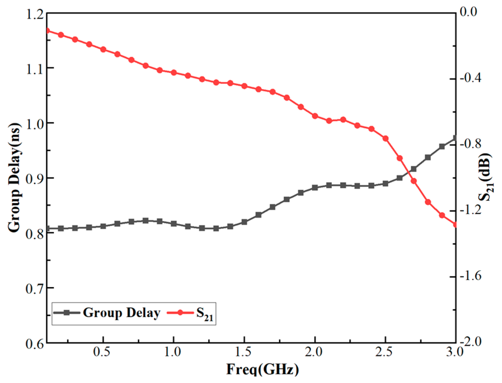
Despite these advancements, most existing LPFs are still implemented using microstrip lines, which are often associated with higher insertion loss and larger dimensions. In this paper, we present a novel self-packaged, high-impedance line LPF based on the SISL technique. This LPF is constructed by converting a microstrip line to an SISL structure. The simulation and measurement results indicate that the LPF achieves a return loss (S11) of less than −15 dB and an S21 greater than −0.74 dB, with a f0 of 3 GHz. Additionally, the group delay in the pass-band is maintained between 0.8 ns and 1 ns, exhibiting excellent linearity. Owing to the high solid-line impedance, which is accompanied by low conductor loss and dielectric loss, the proposed SISL LPF features the internal highest solid-line impedance of 110 Ω. This characteristic significantly enhances signal transmission efficiency in radio frequency (RF) circuits.

2. SISL LPF Design

2.1. The Core Circuit of LPF Design

The design indexes of LPF are shown in Table 1, including that f 0 is 3 GHz and S21 must be less than −15 dB when f is 5 GHz. In addition, the impedance of the filter is 50 Ω, the maximum solid-line impedance is 120 Ω, and the minimum solid-line impedance is 20 Ω.
Meanwhile, the normalized frequency and order are calculated before the filter design; its equations are shown in (1) and (2):
Ω = f f 0
n = f f 0 1
where Ω is the normalized frequency of the filter, f is the stop-band side frequency, f 0 is the cutoff frequency, and n is the order of filter. From (1) and (2), it can be seen that Ω of LPF is 1.6 and the order n is 6. The prototype value of the LPF is described in Table 2. From the Table, g is directly selected from the prototype value, and it can be seen that the prototype value of LPF are as follows: g1 = 0.52, g2 = 1.41, g3 = 1.93, g4 = 1.93, g5 = 1.41, and g6 = 0.52.
To achieve a more compact circuit, the alternating high-/low-impedance structures are utilized in this LPF based on a sixth-order Butterworth topology, as illustrated in Figure 1. This configuration comprises three LC resonator elements: L1 and C1, L2 and C2, and L3 and C3. Additionally, the input and output impedance, R1 and R2, are both set to 50 Ω to ensure compatibility with standard RF systems. The impedance and frequency are adopted to determine the formula, and high-/lo-w-impedance lines are used to replace series inductors and parallel capacitors. The electrical length, actual width, and length of the microstrip line can be calculated by electromagnetic simulation.
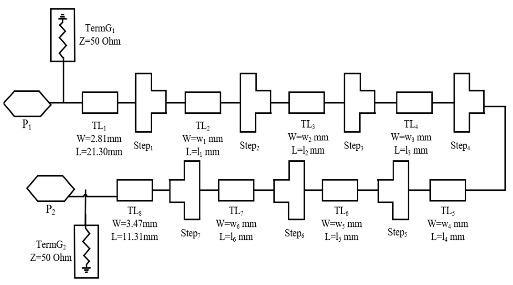
Thus, the schematic of LPF is shown in Figure 2, which shows that the size of the microstrip lines of this LPF are as follows: W1 = 2.81 mm, L1 = 21.30 mm; W2 = 16.20 mm, L2 = 1.24 mm; W3 = 0.29 mm, L3 = 5.13 mm; W4 = 10.89 mm, L4 = 5.06 mm; W5 = 0.31 mm, L5 = 5.76 mm; W6 = 11.99 mm, L6 = 3.73 mm; W7 = 0.38 mm, L7 = 3.25 mm; and W8 = 3.47 mm, L8 = 11.31 mm. It can be seen that the designed filter is composed of six microstrip lines. Because of the discontinuity of microstrip line structure with stepped impedance, the microstrip lines with adjustable length at both ends are added between each line to obtain good filtering performance.
Subsequently, leveraging the constant and unchanging characteristics of the electrical length and impedance of transmission lines, the microstrip line is transformed into an SISL structure. The line length and wavelength of the SISL can be precisely determined based on the impedance of the microstrip line. As depicted in Equation (3), the required line width of the SISL can be calculated by utilizing the wavelength of the SISL and the electrical length of the microstrip line.
w = γ     l
where w denotes the line width of the SISL, while γ and l represent the wavelength of the SISL and the electrical length of the microstrip line, respectively.
Moreover, each microstrip line can be accurately converted into an SISL structure through electromagnetic simulation. The conversion from microstrip line to SISL is illustrated in Figure 3. Specifically, the length of the transmission line TL1 is increased from 21.3 mm to 33.54 mm, while its width is reduced from 2.81 mm to 1.79 mm. Similarly, the dimensions of the other microstrip lines are adjusted according to the same conversion rule.
In addition, the core circuit plays a crucial role in realizing the low-pass functionality of the LPF. As depicted in Figure 4 and Figure 5, the core circuit primarily consists of stripline (SL), GCPW, and SISL. Specifically, the GCPW with a width of 0.41 mm is exposed to air and is tapered at the board edge to facilitate seamless integration with an SMA connector. The SL, with a width of 0.36 mm, serves as the transition element between the SISL and GCPW, ensuring smooth signal propagation. Simultaneously, SISL is mainly composed of two stepped impedance resonators (SIRs) with λg/2. TL2, TL3, and TL4 of SIRs have characteristic impedances of 20 Ω-110 Ω-20 Ω. Meanwhile, TL5, TL6, and TL7 are the SIRs with characteristic impedances of 110 Ω-20 Ω-110 Ω. Ultimately, the dimensions of the suspended lines for the LPF are determined through simulation and optimization, as detailed in Table 3.

2.2. The Proposed SISL LPF Design

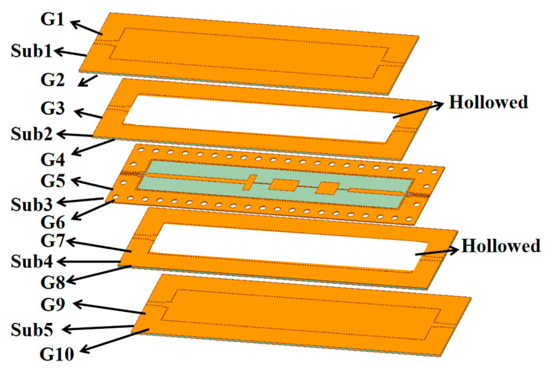
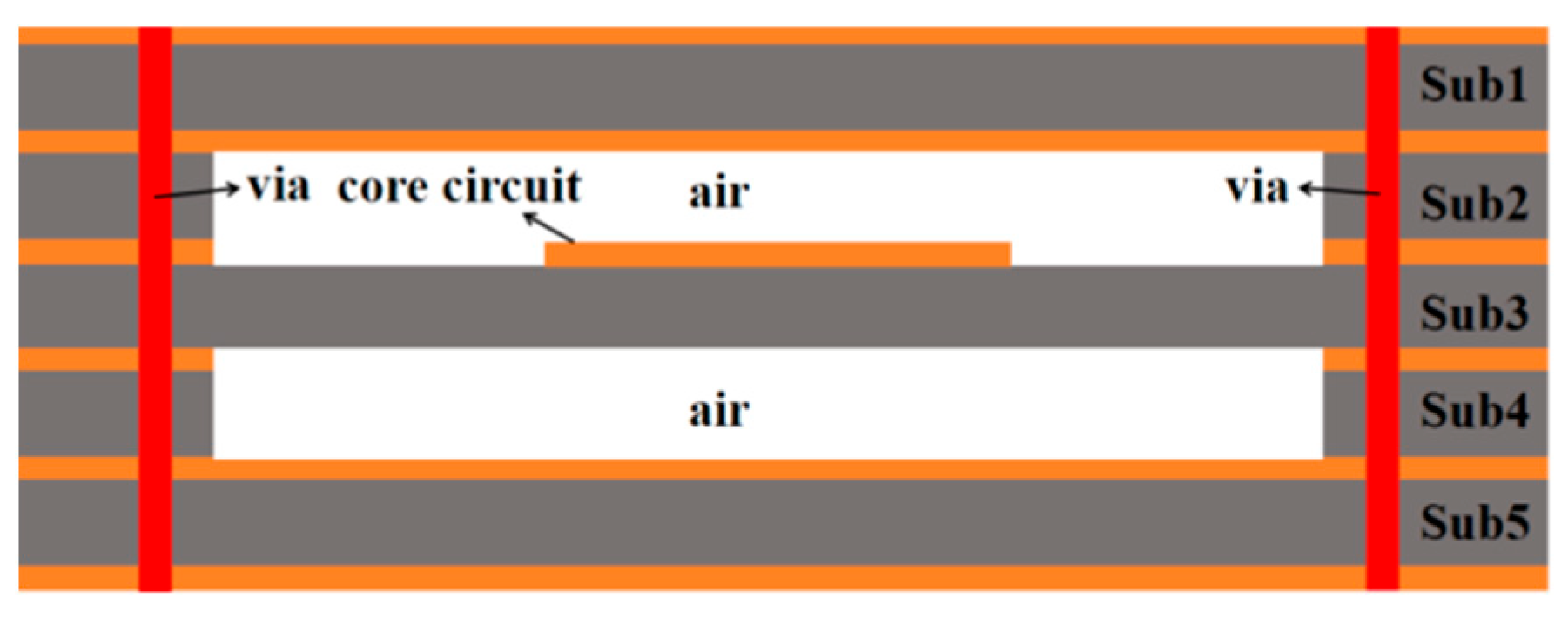
Following the completion of the core circuit design for the LPF, it is integrated into a multi-layer PCB to construct the SISL LPF. The three-dimensional (3D) model and cross-sectional view of the LPF are presented in Figure 6 and Figure 7, respectively.
The SISL LPF is constructed by stacking five substrates in sequence, with each substrate featuring double metal layers. Sub2 and Sub4 are hollowed out around the core circuit, forming the air cavity essential for the SISL LPF. Plated-through vias, labeled from G1 to G10, are strategically arranged around the air cavity to create the metallized sidewalls. Specifically, G2 and G9 serve as the top and bottom conducting boundaries of the suspended line, ensuring proper signal confinement. Moreover, the leakage loss in the SISL is determined by the distance between the via holes, a characteristic that mirrors the behavior of substrate-integrated waveguides (SIWs).
In addition, Rogers RO4350, characterized by a dielectric constant of 3.66, is employed on Sub3 to provide mechanical and electrical support for the suspended line circuit. Meanwhile, FR-4, which has a dielectric constant of 4.4 and is more cost-effective, is utilized on Sub1, Sub2, Sub4, and Sub5. The thicknesses of Sub1 to Sub5 are 0.7 mm, 0.7 mm, 0.254 mm, 0.7 mm, and 0.7 mm, respectively.
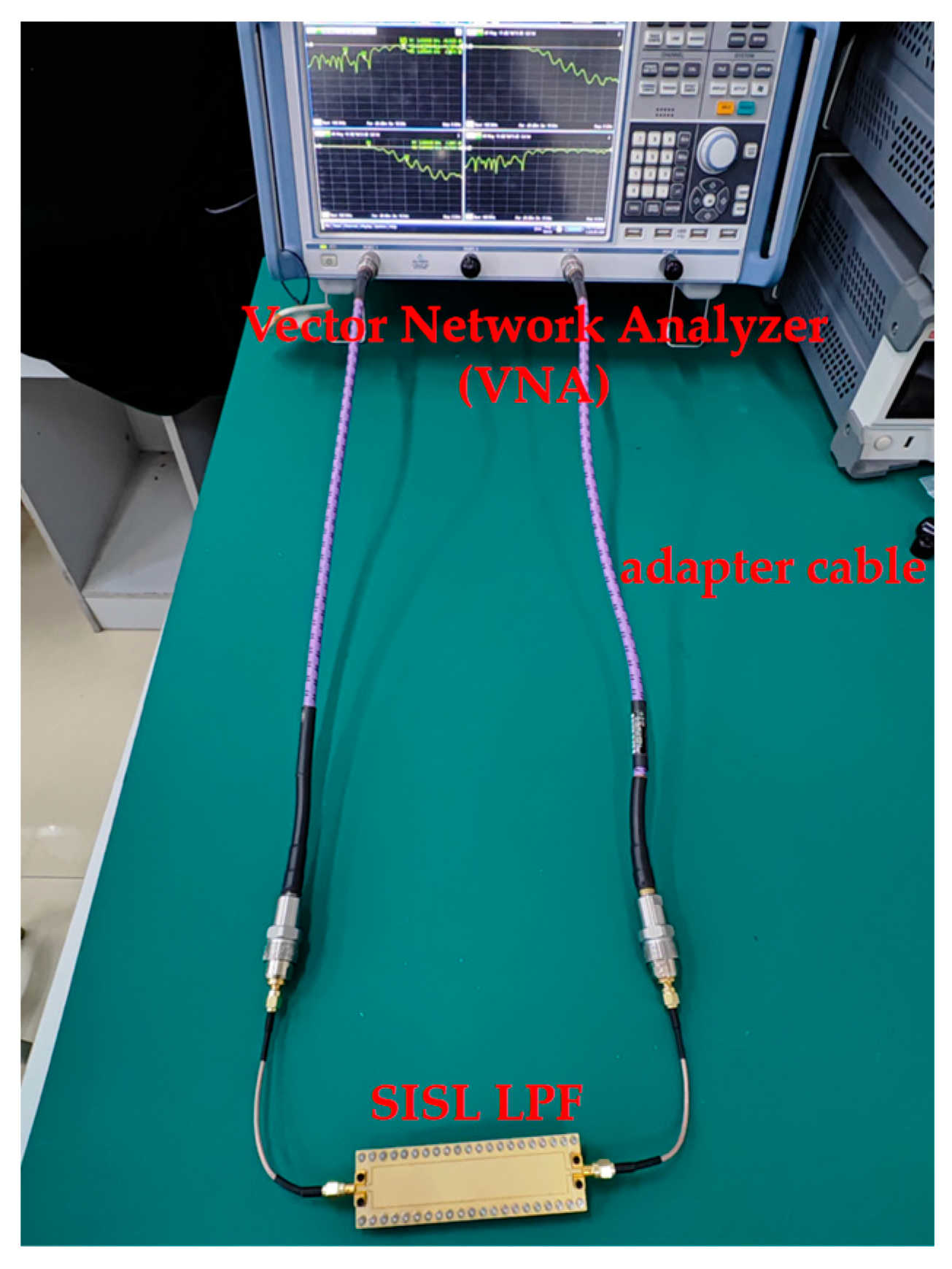
The designed LPF is fabricated with PCB. Both ends of the LPF are connected to a vector network analyzer (VNA) via adapter cables. Among them, the adapter cables merely connect the VNA and the LPF and do not change the transmitted signal. Given that the input and output impedance of the LPF are 50 Ω, it is crucial to ensure correct port connections to the VNA. During the testing process, the start and end frequencies are set to 0.1 GHz and 8 GHz, respectively, with a frequency step size of 5 MHz. Due to the limitations of the experimental setup, the maximum measurable frequency range is from 0 to 8 GHz. The test setup for the LPF is illustrated in Figure 8.
Finally, the photograph of the fabricated LPF is presented in Figure 9. The area of the core circuit is approximately 0.17 λg × 0.98 λg, where λg denotes the guided wavelength at a f0 of 3 GHz. The normalized dimensions of the LPF are 15 mm × 89.47 mm.

3. Results and Analysis

As a passive circuit, the performance of the LPF is characterized by several key parameters: insertion loss (S21), return loss (S11), group delay, and the solid-line impedance. The primary significance of each parameter is as follows:
Firstly, S21 represents the filtering performance of the LPF at a specific frequency, indicating the amount of signal that is transmitted through the filter. The equation for S21 is given in (4).
S 21 = 10     l o g 10 P i n P o u t
where S21 represents the insertion loss, Pin denotes the input power and Pout indicates the output power.
Secondly, S11 characterizes the reflection of the signal back to the source, which is typically greater than 15 dB. It is described by Equation (5).
S 11 = 10     l o g 10 P r e f l e c t e d P i n c i d e n t
where S11 represents the return loss, and Preflected and Pincident are the total power of the reflected wave and the incident wave of the LPF, respectively. In the designed LPF, the S11 is determined by the reflected signal, which can indicate the impedance-matching performance of the wireless communication system [22].
Thirdly, the group delay is defined as the negative value of the derivative of the phase with respect to frequency. It describes the change in time delay of the signal as it passes through the filter. The group delay can be calculated using Equation (6).
T g ( f ) = d φ ( f ) d f
where T g is the group delay of the LPF, φ is the phase response of the system, and f is the measured frequency. Moreover, the linearity of the group delay is one of the important parameters, which can demonstrate the prominent filtering performance of the LPF [23].
Ultimately, the solid-line impedance for this LPF is the inherent impedance of the guided wave, which reflects the distributed characteristics of the electromagnetic field energy in the SISL LPF. It is described by Equation (7).
Z 0 60 ε l n 4 h w
where Z0 is the solid-line impedance, ε is the dielectric constant of the core circuit substrate, h is the thickness of the air cavity, and w is the width of the SISL. The solid-line impedance can significantly influence the frequency response, reduce the insertion loss, and enhance the transmission efficiency within the pass-band.
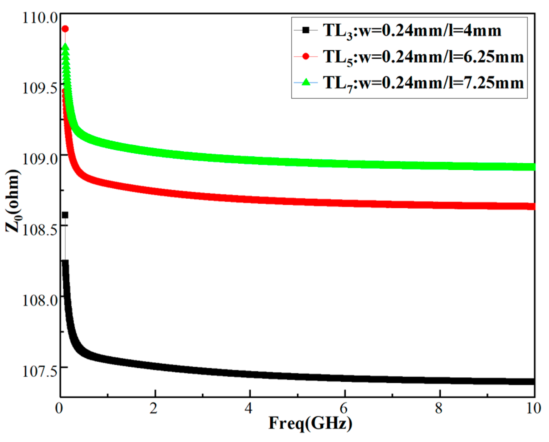
The simulated impedance of the solid line for this LPF is illustrated in Figure 10, showing how the impedance of the suspended line varies with frequency. For a given width of the suspended line, the impedance of the solid line increases as the length of the suspended line increases. The maximum solid-line impedance reaches 110 Ω.
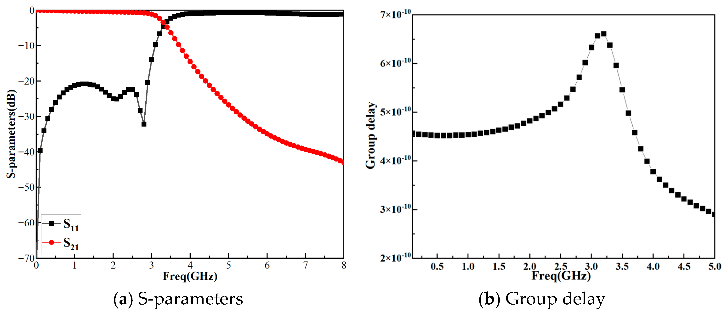
Therefore, the S-parameters of the microstrip LPF are shown in Figure 11a. The results show that the S21 of the filter is greater than −1.01 dB at the frequency range of 0 ~ 3 GHz and the S11 is less than −20 dB within the pass-band of the filter. Finally, the group delay of the microstrip LPF is shown in Figure 11b. It can be seen that the linearity of the group delay is good when filtering within the pass-band.
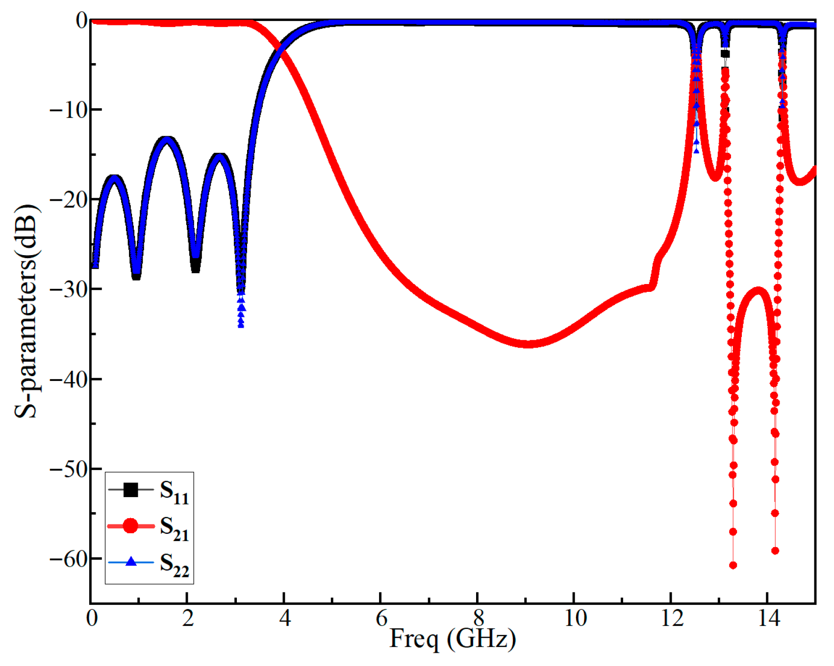
The simulated S-parameters of the LPF from DC to 15 GHz are presented in Figure 12. It is evident that the pass-band extends from 0 to 3 GHz, while the stop-band ranges from 5 to 12.2 GHz. Notably, the simulated stop-band reaches up to 12.2 GHz (2.3 f0), with a stop-band rejection exceeding 15 dB. Meanwhile, according to the S22, the impedance between the filter output and the load is matched and the signal can be transmitted more efficiently. Compared with microstrip LPF, the S21 of this SISL LPF is lower and the poles of the S11 are clearer. Therefore, this SISL LPF is superior to the microstrip LPF.
Due to the limitations of the experimental setup, the maximum measurable frequency range is from 0 to 8 GHz. The simulated and measured S-parameters of the LPF are compared in Figure 13, where both exhibit a consistent overall trend. To illustrate the performance of the LPF, the simulated S11 and S21 at the cutoff frequency (f0 = 3 GHz) are −21.72 dB and −0.26 dB, respectively. In the measured results, within the pass-band of the LPF, the S11 is less than −15 dB and the S21 is greater than −0.74 dB. Meanwhile, the stop-band rejection reaches approximately −15 dB at 5 GHz, indicating excellent signal quality through the LPF.
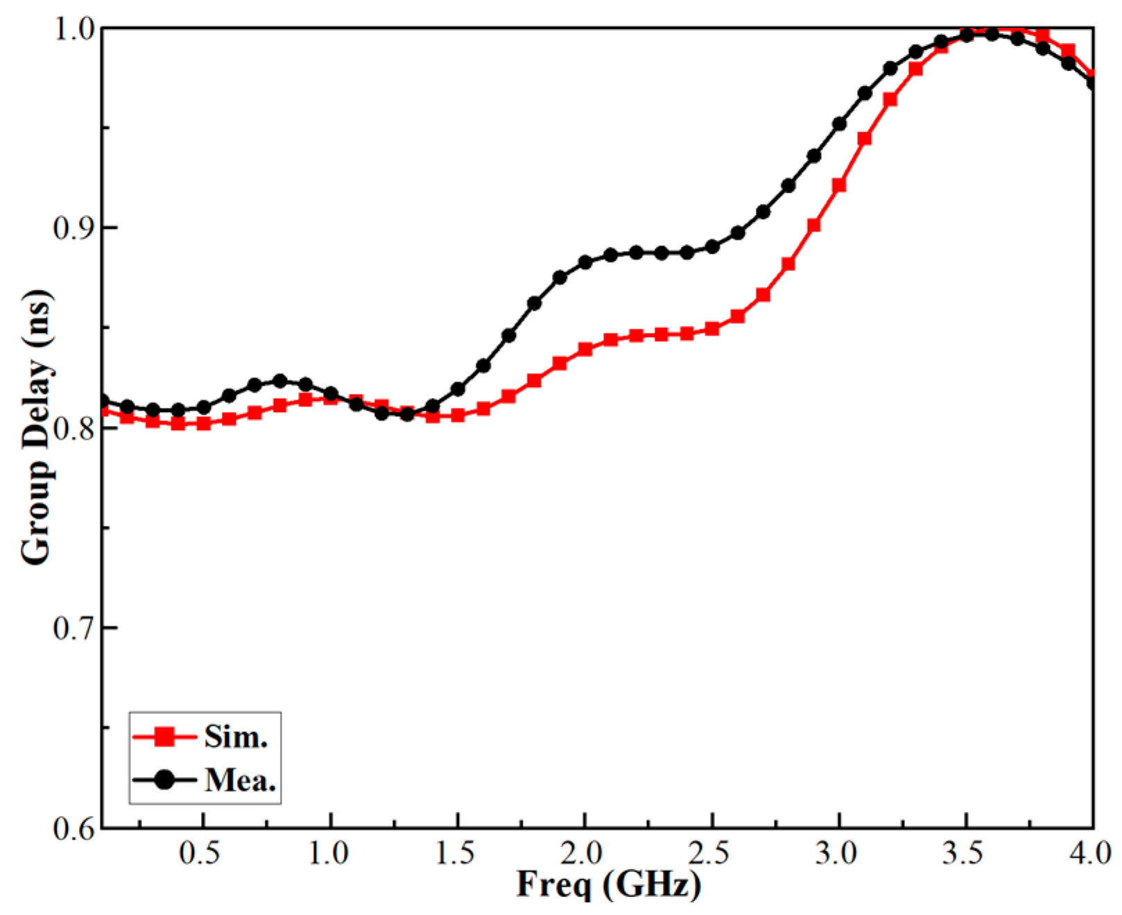
In addition, the simulated and measured group delay of the LPF are compared in Figure 14. It is evident that the group delay remains within the range of 0.8~1 ns from 0 to 3 GHz. This consistency demonstrates the excellent linearity and filtering performance of the proposed LPF.
By comparing the group delay and the S21 of the LPF, as illustrated in Figure 15, it is evident that these two parameters exhibit a linear correlation. Specifically, the group delay increases steadily as the S21 decreases, with the overall range of group delay maintained between 0.8 ns and 1 ns.
Ultimately, the S-parameters and group delay of the LPF are meticulously simulated and optimized through advanced electromagnetic simulation techniques. The simulation and measured results collectively demonstrate exceptional signal quality through the LPF, achieving all anticipated performance metrics. When juxtaposed against other technologies of LPFs, such as DGS, SMD, LTCC, and microstrips, this LPF stands out with its self-packaging capability. Furthermore, compared to other SISL LPFs of the same category, the proposed LPF boasts a higher internal solid-line impedance, with an S21 of 0~−0.7 dB in the pass-band of 0~3 GHz, which indicates remarkably low insertion loss. This elevated impedance translates to reduced conductor and dielectric losses. Coupled with the intrinsic low-loss characteristics of the self-packaging structure, the final insertion loss of this LPF is maintained above −0.7 dB, as detailed in Table 4.

4. Conclusions

In this paper, a self-packaged, high-impedance line LPF based on SISL technology is presented. By incorporating various types of transmission lines, the SISL LPF exhibits exceptional low-pass and filtering performance. Among them, the LPF achieves a S11 of less than −15 dB and an S21 greater than −0.74 dB, with a f0 of 3 GHz. In addition, the group delay is maintained between 0.8 ns and 1 ns within 0~3 GHz, demonstrating excellent linearity. Specifically, the proposed SISL LPF features the internal highest solid-line impedance of 110 Ω. Therefore, the S11, S21, group delay, and the solid-line impedance all demonstrate remarkable frequency responses. Ultimately, the designed LPF leverages the advantages of a high-impedance line, low insertion loss, and self-packaging enabled by the SISL technique. These characteristics provide a significant foundation for optimizing filtering performance in practical applications. In the future, the all-metal substrate to replace the current five-layer substrate will be considered to reduce the dielectric loss of the existing filter and improve its performance.

Author Contributions

Methodology, Q.L., Y.W. and S.L.; Software, Y.W. and S.L.; Writing—original draft, X.W.; Writing—review & editing, Q.L.; Supervision, Q.L., H.W. and S.L.; Project administration, Q.L., H.W. All authors have read and agreed to the published version of the manuscript.

Funding

This research was funded by the Qinghai Science and Technology plan-surface project: 2025-ZJ-954M.

Data Availability Statement

The raw data supporting the conclusions of this article will be made available by the authors on request.

Conflicts of Interest

The authors declare no conflict of interest.

References

  1. Liu, L.; Liu, X. All-optical tunable microwave filter with ultra-high peak rejection and low-power consumption. Opt. Express 2020, 28, 13455–13465. [Google Scholar] [CrossRef] [PubMed]
  2. Feng, L.P.; Zhu, L.; Zhang, S. Differential-mode low-pass filter using hybrid CPS and G-CPS with intrinsic common-mode rejection. IEEE Trans. Microw. Theory Tech. 2019, 67, 1836–1843. [Google Scholar] [CrossRef]
  3. Han, Y. A flexible microstrip low-pass filter design using asymmetric pi-shaped DGS. IEEE Access 2019, 7, 49999–50006. [Google Scholar] [CrossRef]
  4. Feng, J.; Wang, X.; Poterjoy, J. A Comparison of Two Local Moment-Matching Nonlinear Filters: Local Particle Filter (LPF) and Local Nonlinear Ensemble Transform Filter (LNETF). Mon. Weather Rev. 2020, 148, 4377–4395. [Google Scholar] [CrossRef]
  5. ElIssawi, M.L.; Konditi, D.; Usman, A.D. Design of Enhanced Wide Band Microstrip Patch Antenna Based on Defected Ground Structures (DGS) for Sub-6 GHz Applications. Int. J. Electr. Electron. Res. 2024, 12, 315–321. [Google Scholar] [CrossRef]
  6. Shi, L.F.; Fan, Z.Y. Miniaturized low-pass filter based on defected ground structure and compensated microstrip line. Microw. Opt. Technol. Lett. 2020, 62, 1093–1097. [Google Scholar] [CrossRef]
  7. Al-hussein, A.; Luhaib, S. Design and miniaturized a high suppression stop band microstrip low pass filter by using slot defected ground structure for 5G applications. AREJ Al-Rafidain Eng. J. 2024, 29, 126–131. [Google Scholar]
  8. Khairi, K.A.; Jamlos, M.F.; Padmanathan, S.; Jamlos, M.A.; Isa, M.M. Low insertion loss of surface mount device low pass filter at 700 MHz. Bull. Electr. Eng. Inform. 2019, 8, 382–388. [Google Scholar] [CrossRef]
  9. Lee, T.H.; Lee, B.; Kim, Y.S.; Wu, K.; Lee, J. Higher order lumped element absorptive low-pass and band-pass filter structures. IET Microw. Antennas Propag. 2019, 13, 1166–1173. [Google Scholar] [CrossRef]
  10. Yuan, B.; Mou, J.; Tong, L.; Lv, X. A miniaturized LTCC lowpass filter with two transmission zeros. In Proceedings of the 2011 4th IEEE International Symposium on Microwave, Antenna, Propagation and EMC Technologies for Wireless Communications, Beijing, China, 1–3 November 2011; pp. 221–223. [Google Scholar]
  11. Zheng, Y.; Sheng, W. Compact lumped-element LTCC band-pass filter for low-loss VHF-band applications. IEEE Microw. Wirel. Compon. Lett. 2017, 27, 1074–1076. [Google Scholar] [CrossRef]
  12. Lotfi, S.; Roshani, S.; Roshani, S.; Janda, M.; Blecha, T. Design of a compact low-pass filter with an ultra-wide stop-band using triangular Resonators. In Proceedings of the 2024 47th International Spring Seminar on Electronics Technology, Prague, Czech Republic, 15–19 May 2024; pp. 1–4. [Google Scholar]
  13. Chemseddine, F.M.; Rahmouna, E.; Didier, V. A Design of Microstrip Low-pass Filter using ground-plane coplanar waveguide. Telecommun. Radio Eng. 2024, 83, 1–8. [Google Scholar] [CrossRef]
  14. Shome, P.P.; Khan, T.; Koul, S.K.; Antar, Y.M. Two Decades of UWB Filter Technology: Advances and Emerging Challenges in the Design of UWB Band-pass Filters. IEEE Microw. Mag. 2021, 22, 32–51. [Google Scholar] [CrossRef]
  15. Snyder, R.V.; Macchiarella, G.; Bastioli, S.; Tomassoni, C. Emerging trends in techniques and technology as applied to filter design. IEEE J. Microw. 2021, 1, 317–344. [Google Scholar] [CrossRef]
  16. Ma, K.; Chan, K.T. Quasi-Planar Circuits with Air Cavities. PCT Patent WO 149046, 27 December 2007. [Google Scholar]
  17. Ma, Z.; Ma, K.; Mou, S. An ultra-wide stopband self-packaged quasi-lumped-element low pass filter based on substrate integrated suspended line technology. In Proceedings of the 2017 IEEE MTT-S International Microwave Symposium, Honololu, HI, USA, 4–9 June 2017; pp. 1084–1087. [Google Scholar]
  18. Ma, Z.; Ma, K.; Mou, S.; Meng, F. Quasi-lumped-element filter based on substrate-integrated suspended line technology. IEEE Trans. Microw. Theory Tech. 2017, 65, 5154–5161. [Google Scholar] [CrossRef]
  19. Wang, Y.; Yu, M.; Ma, K. A compact low-pass filter using dielectric-filled capacitor on SISL platform. IEEE Microw. Wirel. Compon. Lett. 2021, 31, 21–24. [Google Scholar] [CrossRef]
  20. Zhang, H.; Wang, Y.; Ma, K. A compact low-pass filter using a miniaturized capacitor and honeycomb cavity on substrate integrated suspended line platform. IEEE Microw. Option Technol. Lett. 2023, 65, 1843–1849. [Google Scholar] [CrossRef]
  21. Pozar, D.M. Microwave Engineering, 4th ed.; Wiley: Hoboken, NJ, USA, 2019. [Google Scholar]
  22. Xie, M.Z.; Wang, L.F.; Zhou, B.B.; Huang, Q.A. An impedance matching method for LC passive wireless sensors. IEEE Sens. J. 2020, 20, 13833–13841. [Google Scholar] [CrossRef]
  23. Shao, T.; Wang, Z.; Fang, S.; Liu, H.; Chen, Z.N. A full-pass-band linear-phase band-pass filter equalized with negative group delay circuits. IEEE Access 2020, 8, 3336–43343. [Google Scholar] [CrossRef]
Figure 1. Schematic of this LPF.
Electronics 14 04139 g001
Figure 2. Schematic of the microwave LPF.
Electronics 14 04139 g002
Figure 3. Conversion from micro-strip line to SISL.
Electronics 14 04139 g003
Figure 4. Core circuit of this LPF.
Electronics 14 04139 g004
Figure 5. Planar view of G5 for this LPF.
Electronics 14 04139 g005
Figure 6. Three-dimensional model of this LPF.
Electronics 14 04139 g006
Figure 7. Cross-section view of this LPF.
Electronics 14 04139 g007
Figure 8. Test setup of this LPF.
Electronics 14 04139 g008
Figure 9. Photograph of this LPF.
Electronics 14 04139 g009
Figure 10. Simulated solid-line impedance of this LPF.
Electronics 14 04139 g010
Figure 11. Simulated curves of the microstrip LPF.
Electronics 14 04139 g011
Figure 12. Simulated S-parameters of this LPF from DC to 15 GHz.
Electronics 14 04139 g012
Figure 13. Simulated and measured S-parameters of LPF.
Electronics 14 04139 g013
Figure 14. Simulated and measured group delay of this LPF.
Electronics 14 04139 g014
Figure 15. Compared group delay and S21 of this LPF.
Electronics 14 04139 g015
Table 1. Design indexes of LPF.
PerformanceIndex
f03 GHz
S21 (f = 5 GHz)<−15 dB
Max solid-line impedance120 Ω
Min solid-line impedance20 Ω
Table 2. Prototype value of the LPF [21].
ng1g2g3g4g5g6g7g8
12.001.00
21.411.411.00
31.002.001.002.00
40.771.851.850.771.00
50.621.622.001.620.621.00
60.521.411.931.931.410.521.00
70.451.251.802.001.801.250.451.00
Table 3. Sizes of suspended lines for LPF.
VariableLength/mmVariableLength/mm
w11.79L133.54
w27.8L22.28
w30.24L36.25
w45.35L48.9
w50.24L57.25
w65.99L66.46
w70.24L74
w81.79L818.11
Table 4. Performance comparison with other similar LPFs.
Referencesf0/GHzIL/dBRL/dBTechniqueSelf-Packaging
[6]2.2>−0.8<−10DGSNo
[8]0.7>−1NA*SMDNo
[10]1>−0.7<−18LTCCNo
[12]2.2>−0.7<−22MicrostripNo
[18]1>−1.2<−25SISLYes
[20]0.6>−2.2<−15SISLYes
This work3>−0.7<−15SISLYes
NA*: the data are not available in the reference.
Disclaimer/Publisher’s Note: The statements, opinions and data contained in all publications are solely those of the individual author(s) and contributor(s) and not of MDPI and/or the editor(s). MDPI and/or the editor(s) disclaim responsibility for any injury to people or property resulting from any ideas, methods, instructions or products referred to in the content.