1. Introduction
Rapid growth of artificial intelligence has led to the widespread use of DNNs in applications such as natural language processing and autonomous driving. These applications require complex DNN models and intensive computational operations. As models grow, communication between memory and processing units becomes a significant bottleneck, known as the memory wall. This results in high latency and excessive energy consumption, especially in edge computing, where power efficiency is critical.
Traditional solutions, such as hierarchical cache designs and advanced memory technologies, have struggled to meet the growing demands for memory bandwidth. To address this challenge, CIM technology, also known as in-memory computing (IMC), has emerged as a promising alternative. CIM integrates computation directly within memory units, reducing the need for frequent data transfers between memory and processing elements. These units consist of an array of memory elements, such as SRAM cells. This integration not only boosts computational speed but also enhances energy efficiency and increases compute density. A comprehensive survey on CIM processors is presented in [
1], while an overview of in-memory computing circuits for artificial intelligence and machine learning applications is provided in [
2].
Several types of CIM architectures exist, including SRAM-based, DRAM-based, and non-volatile memory-based (NVM-based). SRAM-based CIMs are widely adopted due to their reliability and well-established technology. A recent survey on SRAM-based CIM designs is available in [
3]. DRAM-based CIMs provide large memory capacities, making them suitable for large-scale models, though they face challenges related to high-density integration [
2]. NVM-based CIMs, known for their low power consumption, are particularly well-suited for energy-efficient edge computing [
4]. A review on resistive NVM-based CIMs is presented in [
5]. An overview of analog architectures for CIMs and their mapping to actual DNNs is presented in [
6].
A frequently used operation in DNNs is the MAC. The MAC operation is defined as multiplying each of the
R inputs
by the corresponding weight
, and then summing these products to obtain
. The input
and weight
are represented by
M-bit and
N-bit precision, respectively. The MAC operation in CIM can be performed in analog, digital, or time domains [
1]. Although analog-CIM architectures efficiently perform MAC operations, they require ADCs to convert the analog signals into the digital domain [
7,
8]. This conversion constitutes a significant portion of the overall energy consumption of the CIM [
4]. Several techniques have been proposed to reduce the number of ADC conversions [
9,
10,
11,
12,
13,
14]. All of these studies store the bits of a weight
in successive columns of the memory array. Thus, a weight
occupies
N columns of the memory array. For instance, a 4-bit weight occupies four columns of the memory array.
This paper introduces a novel analog-CIM architecture that allows weights to be flexibly organized across both the rows and columns of the CIM array. Although the architecture is general and compatible with all memory-based CIMs, the primary focus of this work is on SRAM-based implementations. Despite the flexibility of the proposed approach, a single ADC operation remains sufficient to digitize the MAC result. In addition, a pipelining scheme is introduced to decouple the analog-domain MAC and ADC operations, thereby reducing the cycle time. Finally, the proposed architecture is evaluated against existing approaches in terms of latency, area, energy consumption, and utilization, with the analysis centered on architectural principles rather than implementation-specific details.
The paper is organized as follows.
Section 2 provides a detailed review of available architectures. The proposed architecture is presented in
Section 3.
Section 4 compares it with previous work. The contributions of the work are discussed in
Section 5.
2. Related Work
The MAC operation is defined as multiplying each of the
R inputs
by the corresponding weight
, and then summing these products to obtain
. An input
is an
M-bit vector:
, where
is the
m-th bit of
. The weight
is an
N-bit vector:
, where
is the
n-th bit of
. Analog-CIM architectures are efficient in performing MAC operations. However, they require ADCs to convert the analog signals into the digital domain [
7,
8].
Analog-to-digital conversion constitutes a significant portion of the overall energy consumption in CIM systems [
4]. Researchers have addressed this challenge either by developing more energy-efficient ADCs or by reducing the number of ADC operations. The use of hybrid ADC structures has been shown to improve both area and energy efficiency, as reported in [
15]. Although the primary focus of this paper is not on ADC design, the hybrid ADC proposed in [
15] is noteworthy. This design integrates a resistor-DAC with a SAR ADC, achieving significant hardware savings compared to conventional SAR and flash ADCs. Specifically, the number of capacitors and comparators is reduced by 87.5% and 93.3%, respectively. The CIM architecture proposed in this work does not mandate a specific type of ADC, and the hybrid ADC described in [
15] can be readily adopted to improve overall efficiency.
Several studies have aimed to reduce the energy consumption of ADCs by decreasing the number of conversions required. In [
9,
10], multi-bit weights are mapped to adjacent columns of the CIM, and the corresponding results are combined in the analog domain using binary-weighted capacitors. The architectures presented in [
11,
12,
13] also employ binary-weighted capacitors but process 2 or 4 bits of the input
per cycle. More recently, ref. [
14] reported a CIM architecture in which sequential charge sharing between adjacent columns replaces the use of binary-weighted capacitors. Furthermore, a phase-change memory-based analog CIM was proposed in [
16], which requires sequential activation of the word-lines, while an RRAM-based CIM was introduced in [
17], where the weights
are repeated and shifted.
In the remainder of this section, prior architectures are reviewed under three categories: bit-serial scheme, binary-weighted capacitor scheme, and sequential-halving scheme.
2.1. Bit-Serial Scheme
The simplest analog-CIM architecture is based on bit-serial architecture [
7]. The input
s are applied to the rows of the CIM array, one bit at a time, starting from the LSB.
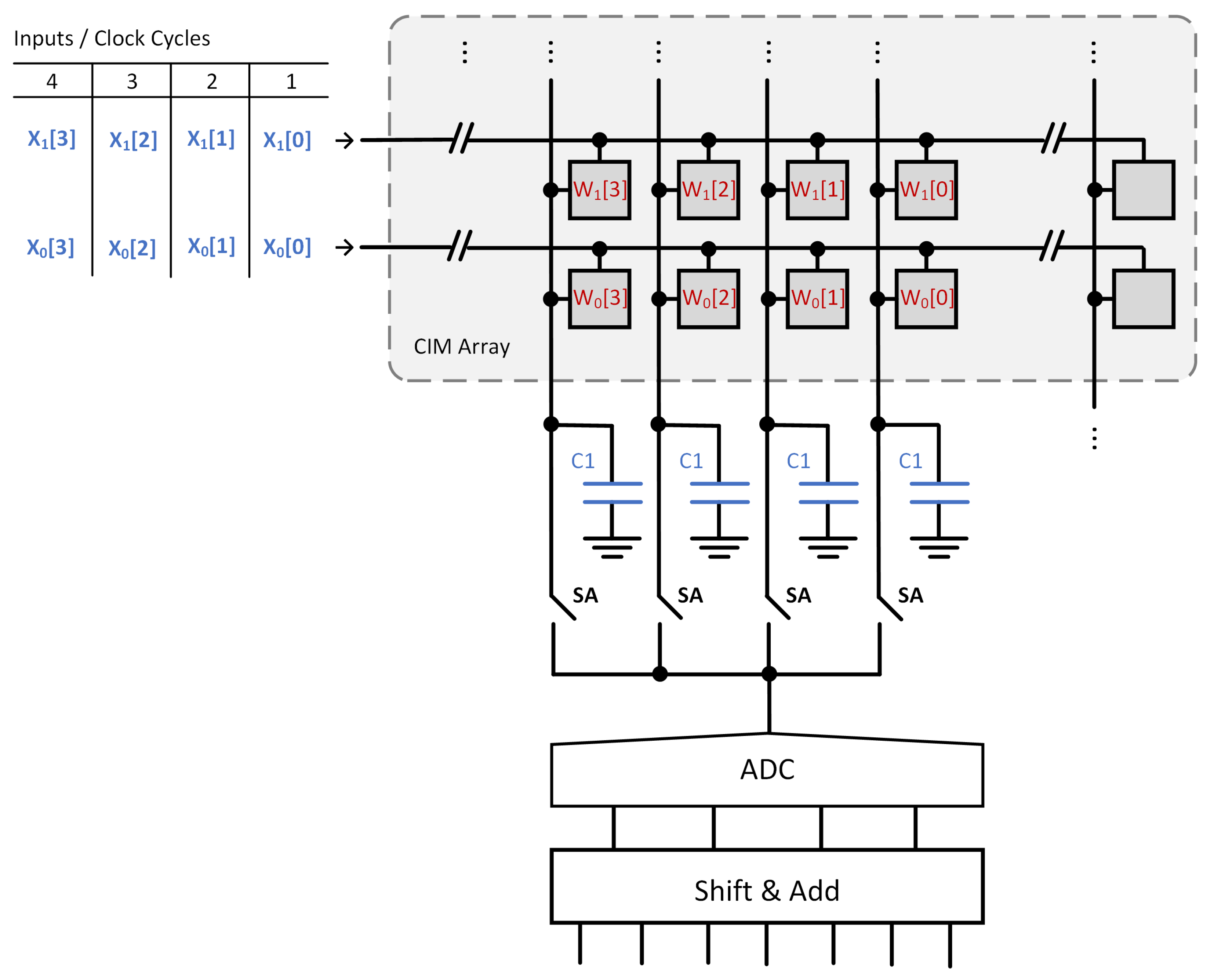
Figure 1 shows a schematic of a simplified bit-serial architecture for
. In this figure, the CIM array has 4-bit weights (
). The entire structure is referred to as the CIM macro, while the section inside the dashed rectangle is the CIM array.
The operating principle of the architecture is explained using the schematic in
Figure 1. The capacitors are first discharged to ground. In the actual implementation, the bit lines are initially pre-charged and then discharged. However, to facilitate a clearer and more straightforward explanation, it is assumed that the bit lines are first discharged to ground and subsequently charged. This simplification is consistently applied to the descriptions of other architectures discussed in this section. When the LSB
s are applied, a potential proportional to
appears on the bit-line capacitors. The ADC then digitizes the potentials stored on the capacitors. The capacitors are then discharged, and the next bits,
s, are applied. The new potentials on the capacitors are proportional to
. After ADC conversion, the new results are shifted and accumulated with the previous ones. This yields
. Repeating this procedure for all input bits results in
. The partial results, one for each bit of the weight
, are then shifted and accumulated to obtain the MAC result
. There are several studies utilizing the bit-serial architecture. The survey in [
1] provides a detailed discussion about these. A recent study [
8] presents a highly efficient implementation that exploits temporal and spatial input correlations to reduce power consumption.
2.2. Binary-Weighted Capacitors Scheme
A novel analog-CIM architecture is presented in [
10]. The architecture supports
-bit inputs and
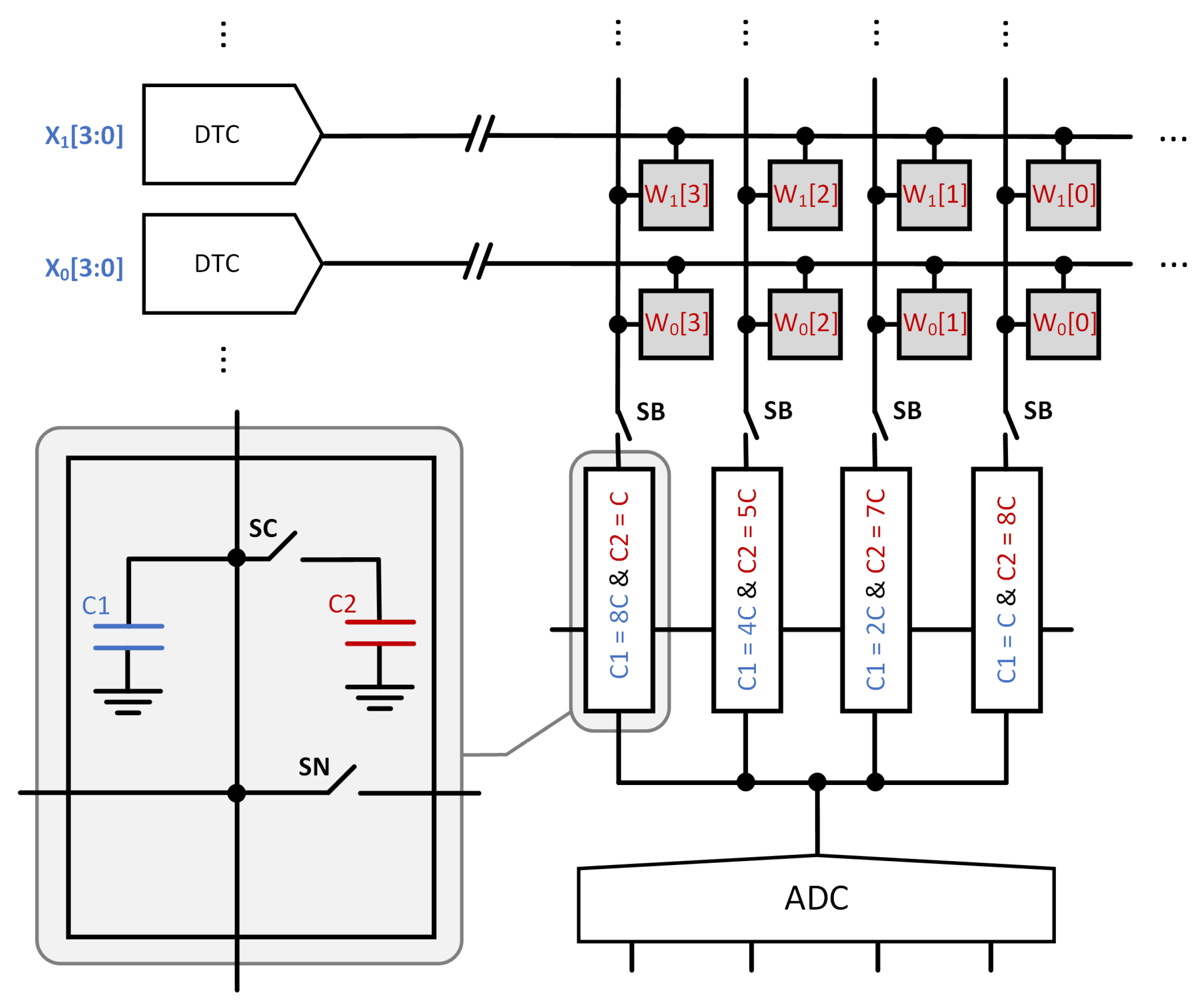
-bit weights. A simplified schematic of the architecture is shown in
Figure 2. The rows of the CIM array are driven by a digital-to-time converter (DTC). An input
is encoded as a sequence of
pulses. For example, if
, the DTC generates 10 pulses. These charge the bit lines proportional to the value of
, enabling MAC computation through charge accumulation.
In
Figure 2, each weight
is stored across four successive columns in a row, with each bit
occupying a single column. The pulses generated by the DTC enable the multiplication of the input
with each bit
, resulting in partial products of the form
. The resulting charges are initially accumulated on a capacitor network with a total capacitance of
. Since all rows are activated simultaneously, the total potential change on the capacitors becomes proportional to the sum of partial products across all inputs as
, where
R denotes the number of rows. Next, the
capacitors and the bit-lines are disconnected from the
capacitors. Thus, the product corresponding to
is stored in the
capacitor with capacitance
, while those corresponding to
,
, and
are stored in the
capacitors with capacitances of
,
, and
C, respectively. Then, all
capacitors are shorted together. This way, the circuit performs the full analog computation
. Finally, 4-bit flash ADC converts the resulting voltage into a digital value.
A similar CIM architecture was presented in [
9]. This circuit also supports
-bit inputs and
-bit weights and uses binary-weighted capacitors. The authors introduced enhancements to the word-line drivers, which deliver the pulses generated by the DTC to the rows of the CIM array. Both circuits in [
9,
10] are designed for 4-bit weights and are not suitable for scaling in the analog domain, as they rely on binary-weighted capacitors. The architectures in [
11,
12] support MAC operations for
-bit inputs and
-bit weights in the analog domain. Similar to [
10], they utilize a binary-weighted capacitor network. For inputs with more than 2 bits, the designs perform successive computations and combine the results using a digital shift-and-accumulate circuit. Likewise, for 8-bit weights, the circuits in [
11] execute two 4-bit computations and reconstruct the final result in the digital domain. These designs also leverage input sparsity to reduce power consumption.
In [
13], the design processes
-bit inputs simultaneously and supports
-bit and
-bit weights. It uses binary-weighted capacitors to perform analog accumulation. The prototype chip, fabricated in 28 nm technology, is reported to achieve a peak 1-bit energy efficiency of 8161 TOPS/W and compute density of 112 TOPS/mm
2. It demonstrates high accuracy on complex DNN benchmarks, achieving 92.34% on CIFAR-10 and 69.88% on ImageNet classification.
2.3. Sequential Halving Scheme
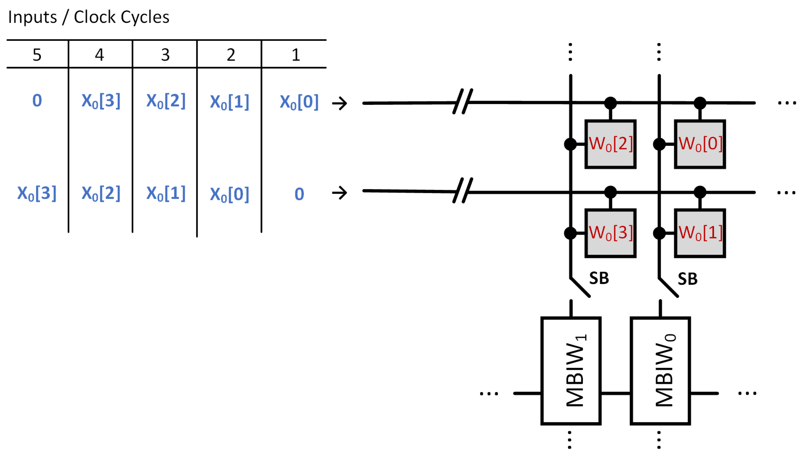
Recently, a new analog-CIM architecture was presented in [
14]. This circuit supports
-bit inputs and
-bit weights. A simplified schematic of the circuit for the
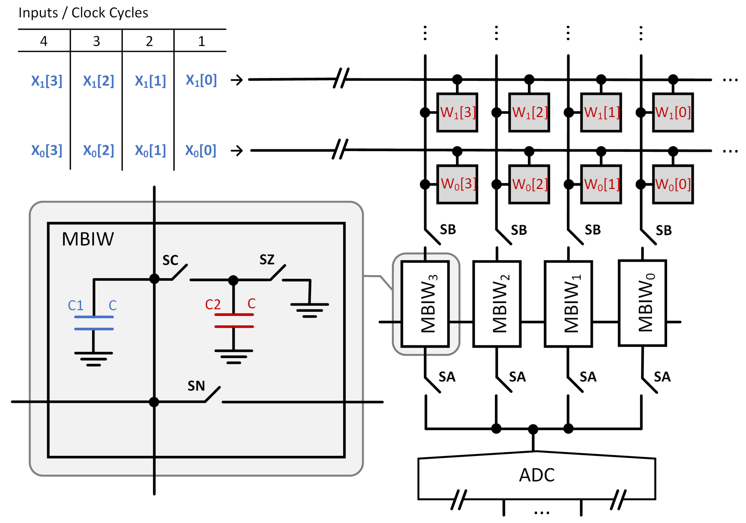
-bit input version is shown in
Figure 3. The columns of the CIM array are connected to multi-bit input-and-weight (MBIW) circuits, which include two equally sized capacitors,
and
, as illustrated in
Figure 3.
The circuit in
Figure 3 operates as follows. First, the LSBs of the inputs
are fed into the CIM array. The resulting charges are stored on the
capacitors in the MBIWs, while the
capacitors are grounded. This sets the potential on each
proportional to
, where
is the weight in the
row and
n is the bit index. Next, the
capacitors are disconnected via SB switches. The
capacitors are then connected to the
capacitors in the same MBIWs. This causes charge redistribution. As a result, the initial potentials on the
capacitors are halved. Now, the potentials on the
and
capacitors in the same MBIW are equal. After this charge sharing, the
capacitors are disconnected. And its potential is proportional to
. Then, the SB is closed and the bit-lines are discharged. Next, the second input bits
are applied. After that, the
and
capacitors are connected. The resulting potential on
is now proportional to
. This process is repeated for the remaining bits of
. After all bits are processed, the final potential on each
capacitor becomes proportional to the binary-weighted sum
. Note that the result is normalized such that the smallest coefficient equals 1. This normalization preserves proportionality and will be consistently applied in the subsequent descriptions.
The operation above results in four separate sums, one for each bit index n of the weights. These sums need to be weighted and added. First, the potential on the capacitor in is halved. This is performed by grounding , then reconnecting it to . After this step, the potential on in becomes proportional to . Then, and are shorted via the switch connecting them. After charge redistribution, the switch is opened. The resulting potential on in will be proportional to . This procedure continues for the remaining MBIWs. After completing all steps, the final potential on the capacitor in becomes proportional to . Finally, an ADC converts the resulting voltage to a digital value.
4. Results
The proposed design is compared against the bit-serial architecture [
7] and the architectures in [
10,
14]. The corresponding implementations for
-bit inputs and
-bit weights are shown in
Figure 1,
Figure 2,
Figure 3 and
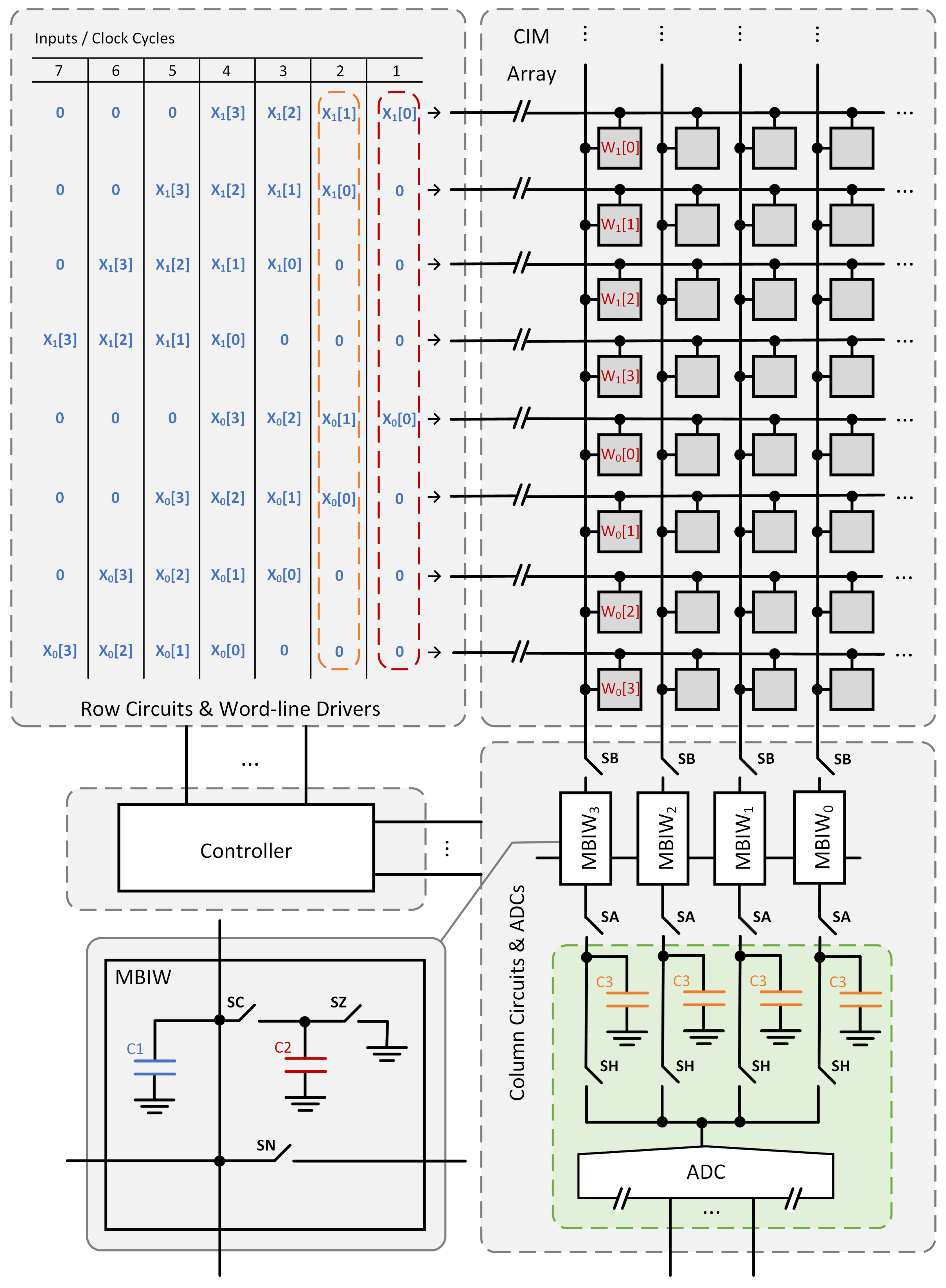
Figure 4. The comparison focuses on architectural principles while deliberately avoiding implementation-specific details. To this end, an event-based simulator was developed. The simulator, available at
https://github.com/ahmetunu/flexible-CIM (accessed on 1 October 2025), reports statistics for latency, area, energy consumption, and hardware utilization. For example, it records the number of bit-line charging operations and ADC activations. These outputs are technology-independent, ensuring fair comparison. This methodology avoids cross-technology bias. The proposed architecture and the previous ones are modeled in this simulator. To verify the correctness of these models, the ADC outputs produced by the macros are validated with the results obtained by directly multiplying the input vector with the weight matrix.
The objective of this study is twofold: (i) to introduce an architecture that enables flexible placement of weights across the rows and columns of the CIM array, and (ii) to propose a pipelining scheme. The design of a specific ADC at a specific technology node is not in the scope of this work. To ensure a fair comparison, the same ADC model is employed across all architectures, with identical reference potentials applied. Thus, any noise introduced by ADC operation affects all designs equally, provided that the same input and reference potentials are used. Since ADC noise depends on its type, resolution, and implementation, using a common ADC ensures that it does not introduce bias into the comparison.
For all designs, the word-line drivers and memory arrays are identical. Likewise, the duration of the word-line pulses and the amount of charge injected by the cells are identical. The capacitor sizes are chosen such that they yield the same potential for
-bit inputs and
-bit weights. To determine the required total capacitance for the proposed architecture and the previous ones [
7,
10,
14], the maximum potential built on the
capacitor is adjusted to be the same. For this purpose, the CIM arrays are filled with ones, and the inputs are also set to ones, yielding the maximum potential on the capacitors.
Table 1 lists the normalized total required capacitance for the proposed architecture and the previous designs [
7,
10,
14]. Bit-line capacitors, which are identical across all designs, are excluded. To give the reader an idea of the order of magnitude, the proposed macro is implemented in 22 nm technology. The required capacitance for each column of the CIM array is 500 fF.
The proposed architecture requires twice the capacitance of the bit-serial design and the same amount as [
14]. The concept presented in [
10] can be extended to
-bit and
-bit inputs. In this case, increasing
M exponentially raises the number of word-line pulses, and the capacitors must be scaled accordingly to maintain the same ADC reference. Even the
-bit implementation requires significantly more capacitance than the other designs. This demonstrates that [
10] does not scale well with input precision.
The analyses are performed for a CIM array of size
with
-bit weights and
-bit inputs. Based on the architectures in [
7,
10,
14], macros are simulated for the same input and weight precision. These designs can perform eight independent
operations at a time. If 16 independent
operations are required on the same macro, they must be operated twice. However, the proposed architecture can execute both 8 independent
and 16 independent
operations within a single macro operation, owing to its flexible weight organization capability. The required number of macro operations for different scenarios is listed in
Table 2 for the proposed architecture and the designs in [
7,
10,
14]. For the proposed architecture, the weight organization
is also provided in the table.
As shown in
Table 1, the proposed architecture requires the same total capacitance as that reported in [
14]. The primary architectural distinction between the two is the inclusion of a programmable delay circuit, described in
Section 3.4. When the weights are organized in the
configuration, this delay circuit acts as a buffer, resulting in operation equivalent to that of [
14], as summarized in
Table 2. The operation of the proposed architecture diverges when the weights are not arranged horizontally across columns. In such cases, the delay circuit adjusts the input timing accordingly, and a different control sequence is applied to the switches, as detailed in
Section 3.2 and
Section 3.3. Consequently, all results obtained for the
configuration are also applicable to the architecture in [
14].
For the
configuration, the latency of the proposed architecture is identical to that of [
14]. A detailed latency comparison between the proposed design and those in [
7,
10] is presented in
Section 4.1. The total area of the proposed architecture and that of [
14] are also very similar, as discussed in
Section 4.2, which further includes comparisons with [
7,
10]. When the weights are organized in the
configuration, the energy consumption of the proposed design closely matches that of [
14], differing by only 0.4 pJ for a 22 nm implementation.
Section 4.3 provides a detailed energy comparison with [
7,
10,
14]. The pipelining scheme described in
Section 3.5 is general and can be applied not only to the proposed approach but also to the architectures in [
7,
10,
14]. In
Section 4.4, the memory utilization of the proposed and prior architectures is compared, while
Section 4.5 reports the performance of the proposed design on the VGG16 network trained on the CIFAR-10 dataset. Finally, the practical limitations of the proposed architecture are discussed in
Section 4.6.
4.1. Latency
The macro begins operation with a bit-line pre-charge phase. Next, pulses are applied to the word-line drivers. The number of pulses varies depending on the architecture and is reported in
Table 3. These pulses activate the word-line drivers, which in turn activate the memory cells. The activated cells charge the bit-lines and the capacitors connected to them. The design in [
10] charges both the
and
capacitors, whereas the proposed design and those in [
7,
14] charge only the
capacitors, as discussed in
Section 2. Next, the word-lines are turned off. Then, depending on the architecture, the switches SC, SZ, SN, SB, and SA are activated, and, finally, the bit-lines are pre-charged again. When SC is closed to redistribute the charge between the
and
capacitors, sufficient time must elapse for the capacitors to reach steady state. Similarly, when SZ is closed, a discharge interval is required for the
capacitor. When SN is closed, a time interval is required for charge sharing between neighboring capacitors. To illustrate the duration of the control signals, the proposed macro is simulated in SPICE with 22 nm transistor models. The resulting control signals are shown in
Figure 8. The ADC is not simulated, and its selection is left to the system designer.
Switching activities along the critical path are reported for two cases: (i) 8 independent
operations (
Table 3) and (ii) 64 independent
operations (
Table 4). If an architecture cannot perform all the sums at once, it is executed the necessary number of times to complete the operations.
Some switches are not present in all architectures. The reader is referred to
Figure 1,
Figure 2,
Figure 3 and
Figure 4 for architectural details. The inputs and weights are sampled from a uniform distribution. Assuming there are eight ADCs in the design (one ADC per eight columns), the number of ADC activations in the critical path is also reported in these tables. The bit-serial design requires intra-column and inter-column digital shift-and-add operations.
Table 3 reports the critical paths for the case of eight independent
operations. The latency of the bit-serial architecture is dominated by the required number of ADC operations, whereas the performance of the architecture proposed in [
10] is limited by the number of required word-line pulses. The proposed architecture and the one in [
14] exhibit same performance.
Table 4 reports the critical paths for the case of 64 independent
operations. Previous approaches [
7,
10,
14] can perform only eight independent MAC operations in a single run. As a result, they utilize only 32 of the 256 available rows in the memory array. In contrast, the proposed architecture can flexibly distribute the weights across both columns and rows, allowing it to perform 64 independent MAC operations in a single run. The latency of the bit-serial architecture is dominated by ADC operations, while that of the architecture in [
10] is dominated by word-line pulses. The proposed architecture requires fewer switching activities and achieves lower latency than the design in [
14]. The exact performance improvement depends on the implementation details and the technology node used.
The critical paths discussed in this section exclude the pipelining scheme presented in
Section 3.5. Pipelining is most effective when the delays of the memory array and the ADC are comparable. In the bit-serial architecture, latency is dominated by ADC operations, whereas in [
10], it is dominated by word-line pulses. Therefore, pipelining has little impact on the overall latency of these architectures. In contrast, pipelining is beneficial for both the proposed architecture and the design presented in [
14]. For the latter, the effect of pipelining is identical to that in the proposed work when the weights are organized in a
configuration. The impact of pipelining on the proposed architecture is summarized in
Table 5.
In
Table 5, the latency reduction achieved by applying pipelining is reported relative to that without pipelining. Since the latencies of the ADC and memory depend on their respective implementations, the results are provided for different ratios of ADC latency to memory latency. As shown in
Table 5, the proposed approach shows a smaller benefit from pipelining as the value of
r increases.
4.2. Area
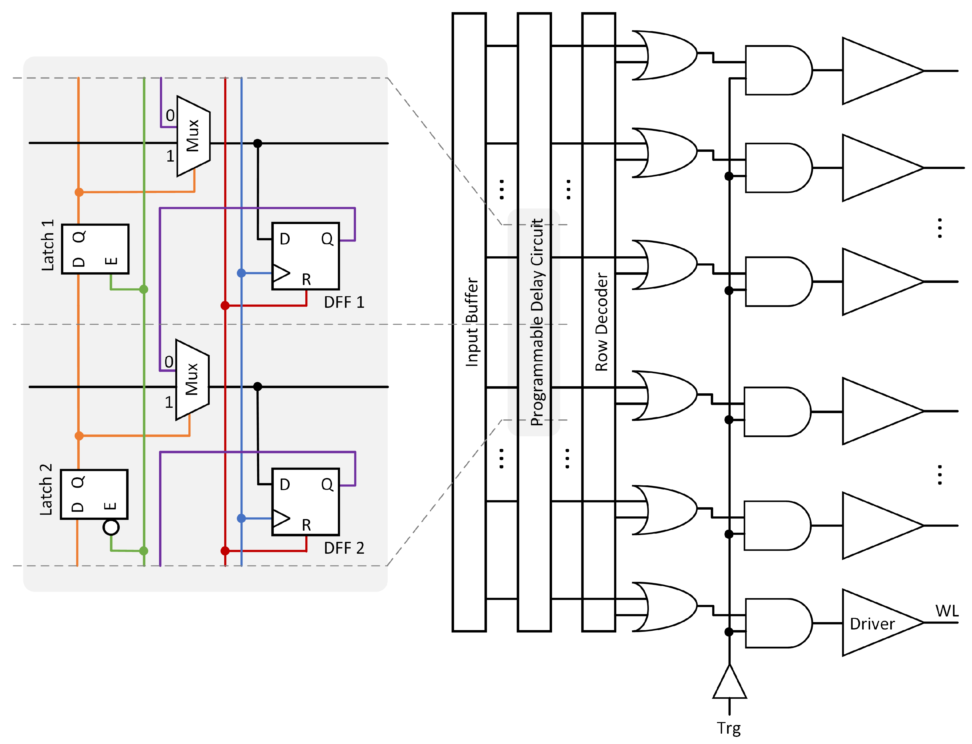
A CIM macro consists of the row circuit, cell array, column circuit, and control logic. A schematic of the row circuitry is shown in
Figure 6, which includes the input buffer, row decoder, basic gates, and word-line drivers. Identical input buffers are used in both the proposed architecture and the previous designs [
7,
10,
14], resulting in equivalent buffer areas. Likewise, the sizes of the word-line drivers and the cell arrays are the same across all architectures. The timing signals and control for the switches are generated by the control logic. Unlike the row or column circuitry, the control logic does not have a periodic structure and occupies only a small portion of the CIM macro. The area difference of the control logic circuits represents a negligible fraction of the total CIM macro and is therefore not analyzed in this study. The designs in [
7,
14] do not require the delay circuit shown in
Figure 6. In contrast, the proposed architecture requires a programmable delay circuit comprising a latch, a D flip-flop, and a multiplexer for each row. The architecture in [
10] utilizes a down counter per row rather than the delay circuit.
The column circuit contains the necessary capacitors, switches, and ADCs, as shown in
Figure 1,
Figure 2,
Figure 3 and
Figure 4.
Table 6 lists the components of the column circuits for both the proposed and previous approaches. Each design uses eight ADCs. However, since this number is identical across all architectures, it is not included in the table. Similarly, the write circuits are identical across all architectures and are therefore not reported in the table. The bit-serial architecture additionally requires shift-and-add circuits, as reported in the table.
The bit-serial architecture requires several shift-and-add circuits. In the approach of [
10], larger capacitors are required in the columns compared to the other designs. The bit-serial architecture does not include any switches, whereas switches are required in the columns of the proposed approach and those in [
10,
14]. The exact areas of the column circuits strictly depend on the utilized technology node. Providing exact figures is beyond the scope of this work.
To provide an estimate of the area, a schematic implementation of a
macro is carried out in 22 nm technology. The required capacitance area is 3200
, assuming MIM capacitors with a capacitance density of 10
. The total gate area of the switches is 33
. In addition, the programmable delay circuit in
Figure 6 requires an extra 8
of gate area.
4.3. Energy Consumption
The proposed approach and the designs in [
7,
10,
14] are compared in terms of energy consumption for two cases: (i) 8 independent
operations (
Table 7) and (ii) 64 independent
operations (
Table 8). Instead of reporting energy consumption for a specific implementation, the events contributing to energy consumption are listed in the tables. Normalized energy consumption for charging the
and
capacitors is also provided. Since the same ADC model is used for all designs, the number of ADC operations is directly proportional to their energy consumption. The number of SA switch activations is identical to the number of ADC operations and is therefore not reported in the tables. If the pipelining scheme in
Section 3.5 is applied to all designs, the number of SH switch activations will likewise equal the number of ADC operations.
The bit-serial architecture requires significantly more ADC operations compared to the other approaches. In contrast, the approach in [
10] turns the word-lines on and off far more frequently than the others. For the case of eight independent
operations, the proposed architecture and the design in [
14] consume comparable amounts of energy.
The designs based on [
7,
10,
14] can execute only eight independent MAC operations in a single run. Consequently, they utilize only 32 rows, even though the memory arrays contain 256 rows. In contrast, the proposed architecture can flexibly distribute the weights across both columns and rows, enabling it to perform 64 independent MAC operations in a single run. Owing to this flexibility, the proposed approach achieves lower energy consumption compared to the others when executing 64 independent
operations.
To provide an estimate of energy consumption, the proposed macro with a CIM array size of
is simulated in SPICE using 22 nm transistor models. The weights are organized in a
format. The energy consumed per MAC operation is 3.2 pJ for the word-line drivers and 14.3 pJ for the pre-charge circuits. The SB and SC switches consume 7.9 pJ and 8.5 pJ, respectively, while the SZ and SN switches consume 0.6 pJ and 1.3 pJ, respectively. The programmable delay circuit in
Figure 6 consumes 0.4 pJ. The total energy consumption per MAC operation of the macro, excluding the ADC and the input buffer, is 46.5 pJ.
4.4. Memory Cell Utilization
Based on the operation performed in the CIM, the percentage of utilized cells in the array varies. Each CIM array contains 256 rows. If an operation requires fewer than 256 inputs, the remaining rows are unused. The proposed approach provides the flexibility to organize weights across both rows and columns, allowing higher memory utilization. For different use cases, the percentage of utilized memory cells is listed in
Table 9.
The proposed architecture supports flexible weight orientations, whereas the other designs in
Table 9 are limited to a
orientation. As a result, the utilization achieved with the proposed architecture is always equal to or greater than that of the other architectures. As reported in the table, it is also possible to arrange
-bit weights in a
orientation by padding with a zero on the right.
4.5. Benchmark Performance
The performance of the proposed architecture is evaluated on the VGG16 network trained on the CIFAR-10 dataset. The kernel size is
for all convolution layers. Number of input channels, number of output channels, and output size are reported in
Table 10 for the convolution layers. The number of terms in each MAC operation, as well as the total number of MAC operations, is also provided. The table also reports CIM macro usage under fixed
and flexible organizations.
As shown in
Table 10, the flexibility of the proposed architecture improves the overall system performance. If the weights are restricted to the
form, 172k CIM macro operations are required per image. In contrast, when the proposed architecture is utilized, the number of CIM macro operations decreases to 153k.
The proposed architecture with a CIM array size of
is simulated in SPICE using 22 nm transistor models. An ADC is not implemented; however, to provide a fair comparison between fixed (
) and flexible weight organizations, identical 6-bit ADCs are assumed in both cases. The ADC is assumed to occupy eight columns, with a latency of 5 ns. For the fixed organization, the macro requires 2.1 ms per inference, corresponding to a throughput of 141 GOPS. The product of an
-bit weight and an
-bit input is considered as one operation when calculating the throughput. With flexible weight organization, the latency decreases to 1.9 ms per inference, resulting in a throughput of 156 GOPS. Assuming an energy dissipation of 10 pJ per ADC conversion in both cases, the fixed and flexible organizations achieve energy efficiencies of 13.6 TOPS/W and 14.7 TOPS/W, respectively. The pipelining scheme described in
Section 3.5 is also applied to evaluate its impact. The clock frequency is dynamically adjusted to maximize performance in different weight organizations. With pipelining, the latency for both the fixed (
) and flexible organizations is reduced to 1.2 ms per inference, resulting in a throughput of 247 GOPS. Thus, pipelining yields a decrease of 43% and 37% in latency for the fixed and flexible organizations, respectively. The corresponding energy efficiencies are 13.8 TOPS/W and 14.4 TOPS/W for the fixed and flexible organizations, respectively.
4.6. Practical Concerns
Although the proposed architecture is general enough to support any precision, in practice, the achievable precision is limited by implementation quality, noise, and mismatches. To assess these limitations, the architecture is implemented in 22 nm technology with a CIM array size of
. The
-bit weights and
-bit inputs are sampled from a uniform distribution. The ADC is not implemented; instead, the resulting potentials are discretized assuming an ideal 8-bit ADC. The macro successfully performs the MAC operation, but with 2-bit precision loss. Therefore, for this specific implementation, even an ADC with 6-bit precision is sufficient. Moreover, mismatches of 1%, 2%, 5%, and 10% between the
and
capacitors in
Figure 4 and
Figure 5 result in precision losses of 2, 3, 4, and 5 bits, respectively. An improved implementation may achieve full 8-bit output precision. However, from a practical standpoint, achieving precision beyond 8 bits remains challenging.
The macro is tested with the VGG16 network, trained on the CIFAR-10 dataset. The baseline accuracy of the network is 93.5%. When the MAC results include 2-bit errors, the accuracy decreases only slightly to 93.4%. However, the effect of a 2-bit precision loss is more pronounced on the larger ImageNet dataset. In [
18], a 2-bit precision loss at the output of CIM macros during ImageNet classification is reported to reduce accuracy by approximately 7–15%, depending on the network. In cases where there is a precision loss of 3, 4, or 5 bits due to mismatches between the
and
capacitors, the corresponding accuracies of the VGG16 network on the CIFAR-10 dataset become 92.6%, 85.1%, and 33.3%, respectively.
