1. Introduction
In recent decades, transformerless grid-connected PV systems have been widely developed and applied in both commercial and residential structures to achieve high efficiency, low-output AC-current distortion, low cost, and CM voltage reduction and a low ground leakage current. There are several review papers reported in the literature which cover the topology modifications and PWM methods that to provide the properties of these grid-connected photovoltaic systems [
1,
2,
3,
4,
5].
Transformerless inverters have been developed and improved over many years and are successfully used commercially in distributed PV grid-connected systems. The S-PT string PV inverters are the common configuration for low power applications (mainly residential applications up to 5 kW). These inverters feature reduced cost, increased efficiency, and minimized its complexity; however, the lack of an isolation source may generate a CM leakage current that flows through the parasitic capacitance of the PV panels [
2]. This unwanted CM noise can increase system losses, cause electromagnetic interference (EMI), increase output harmonics, and lead to safety issues [
6].
One of the most important criteria for evaluating the topology of any grid-connected PV system is the ability to suppress the leakage current and CM noise to an acceptable value, as well as the acceptable total harmonic distortion (THD). Various techniques have been proposed to keep the total CM voltage constant in all operating modes of the inverter and thus eliminate the leakage current [
1,
2,
4,
5,
7,
8,
9,
10]. Both the leakage current and THD vary according to the selected inverter topology and modulation technique used.
In S-PT PV systems, there are three basic methods used to eliminate or suppress the leakage current [
2,
9,
10,
11]: (1) decoupling the PV side from the grid side; (2) clamping the middle point of the splitting DC capacitors; (3) attaching the neutral point of the grid and the negative terminal of the PV source to a common ground [
12].
The connection standards for PV inverters establish a maximum total harmonic distortion of 5% [
13]. The IEC 60755 standard defines the detail requirements for the leakage current protection devices. According to this standard, the leakage current must not exceed 300 mA [
14,
15]. In many advanced industrial topologies of the low-power S-PT inverter, the leakage current must not exceed 50 mA, otherwise the inverter would be automatically disconnected from the power grid.
Parameters of the electrical energy produced by the PV cells strongly depend on the PV inverter control method. Usually, the entire modulation process control is assured by the microprocessor [
7,
15,
16]. The control system of the grid-tied inverter must provide three main requirements:
The maximum power generated in photovoltaic cells should be delivered to the grid under various conditions of solar irradiance and temperature [
7,
17,
18,
19];
The energy generated by the PV system and delivered to the grid should meet the quality requirements, while minimizing reactive power [
18,
19];
The detection and implementation of anti-island protection [
18,
19].
Because the power generated in PV cells must be delivered to the one-phase AC grid, the reference current must therefore be synchronized with the grid voltage in order to maximize the active power delivered from PV cells [
20].
In this paper, the most important functional blocks necessary to explain the operation, test performance, and energy efficiency for different load conditions of the proposed S-PT inverter are presented. All relationships between voltages, currents, and powers at the input and output of the inverter were formed by connecting the inverter output to the load resistor.
This paper is organized as follows:
Section 2 describes the operation modes and characteristics of the proposed S-PT three-level inverter in CHB configuration. This section also presents two-phase DC-DC boost converters that are fed from the string panel output at a level determined by the maximum power point tracking (MPPT) algorithm and are used to stabilize the output DC-link voltage at the level determined by the reference voltage. In addition, this Section presents the implementation of a complete gate control system with galvanic isolation for all IGBTs.
Section 3 presents a multifunctional control system based on the TMS320LF2407 microcontroller and its peripherals, providing a reliable and stable connection of the described inverter into the grid.
Section 4 presents the PSPICE simulation and the measurement results of the proposed S-PT three-level inverter in CHB configuration. The conclusions are given in
Section 5.
2. Implementation of S-PT Three-Level Inverter in CHB Configuration
Three-level inverters have an advantage over two-level inverters due to the increased output voltage level, decreased voltage stress on switching devices, the ability to lower CMV (Common Mode Voltage) and leakage current in many ways, reduced EMI noise, and THD factors [
1,
2,
4,
5,
6,
7,
8,
9,
10].
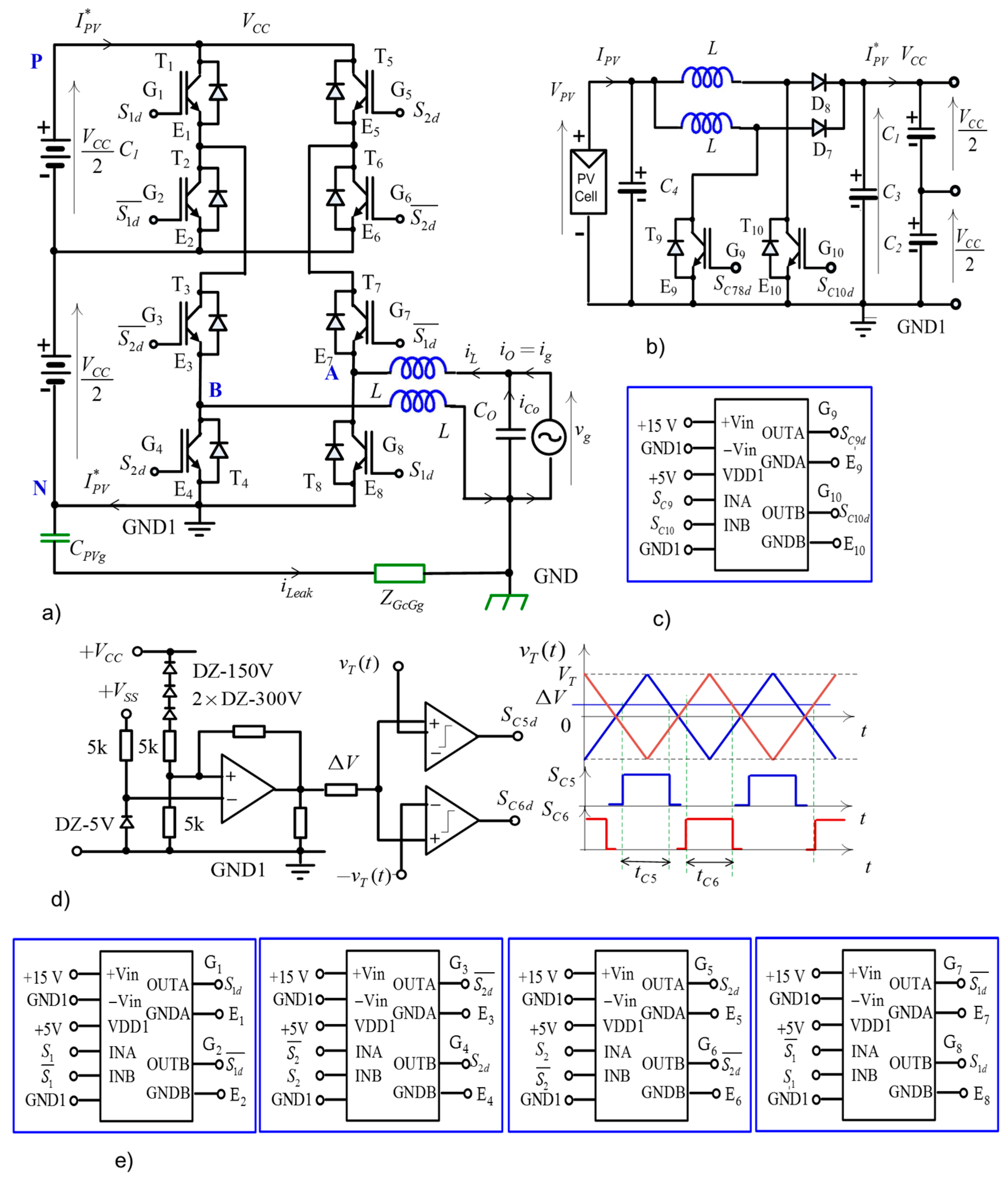
The proposed S-PT inverter in CHB configuration and block diagrams of the IGBT control systems are shown in
Figure 1. The inverter consists of two cascaded H-bridges forming a bridge system with symmetrical inductor configuration. The DC-link voltage
VCC, generated by a string PV panel, is created by two serial voltage sources with a voltage twice as low as the DC-link voltage.
The three-level voltage (+
VCC, 0, −
VCC) at the DM output of the inverter is achieved by switching the IGBTs in the CHB configuration using the DPWM control signals generated by the extended PSCPWM modulator described in [
21].
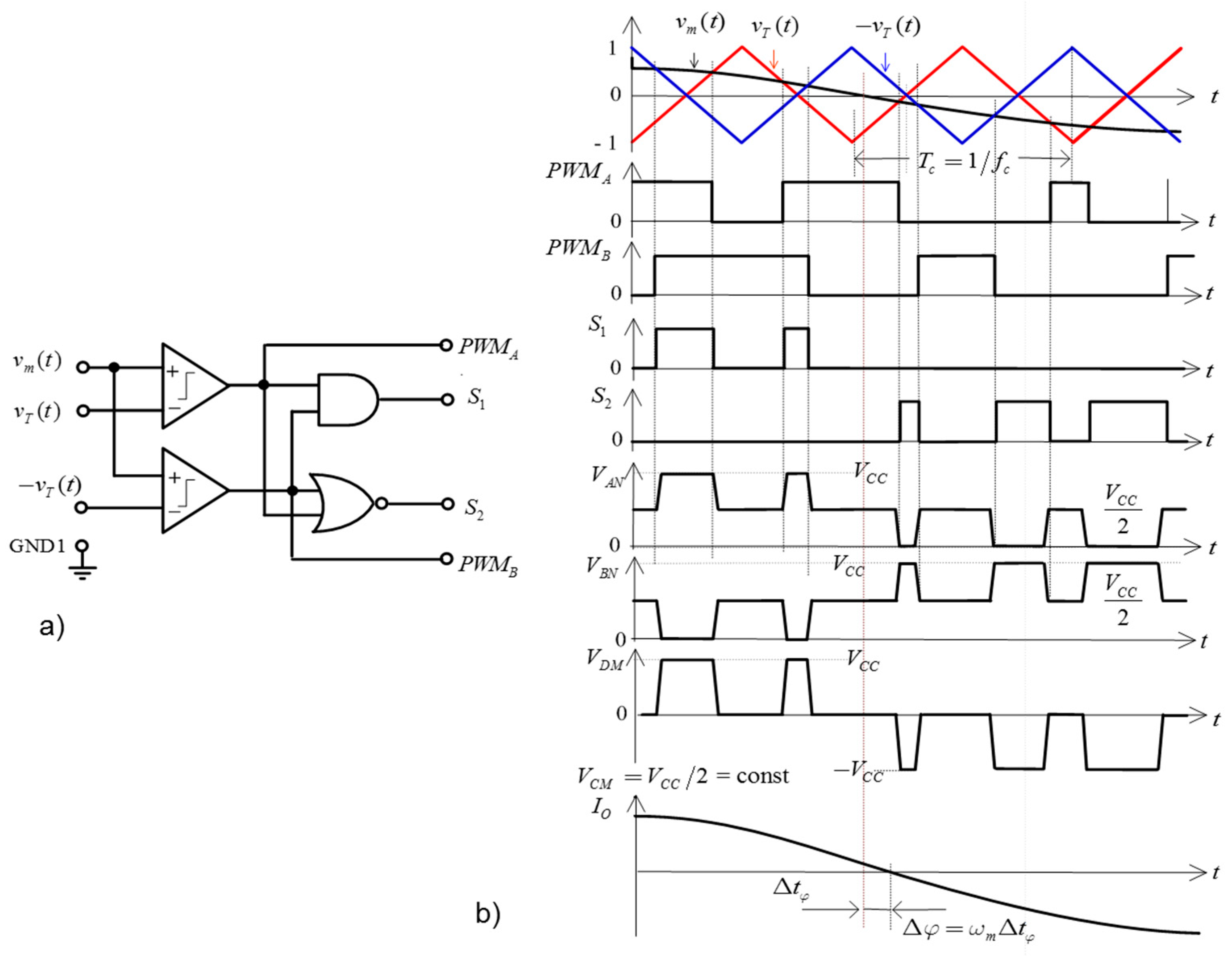
Figure 2 shows the block diagram of the extended PSCPWM modulator and time-domain waveforms of the generated gate signals, as well as the output voltage and current waveforms of the inverter. The analog PSCPWM modulation scheme (referred to as SPWM) was used only to explain the operation principle of the extended PSCPWM modulator. In practice, an extended digital 9-bit linearized PSCPWM modulator based on the STM32F407VGT6 microcontroller was implemented using a counter method algorithm [
22].
As a result of IGBT switching, there are four modes of operation:
Mode 1: T1, T3 and T8 are turned ON, which is the positive half-period in the active state, and all other switches are turned OFF. The current during this mode flows through T1, T3 and T8, resulting in VDM = VAB = VCC, with a CM voltage of VCM = (VAN + VBN)/2 = VCC/2.
Mode 2: T3, T7, T6 and T2 are turned ON, which is the positive half-period in the freewheeling (zero) state, and all other switches are turned OFF. The current during this mode flows through T3, antiparallel diode D7. T6 and antiparallel diode D2, resulting in VDM = VAB = 0, and VCM = (VAN + VBN)/2 = VCC/2.
Mode 3: T5, T7 and T4 are turned ON, which is the negative half-period in the active state, and all other switches are turned OFF. The current flows in the opposite direction through T5, T7 and T4, resulting in VDM = VAB = −VCC, and CM voltage: VCM = VCC/2.
Mode 4: T3, T7, T6 and T2 are turned ON, which is the negative half-period in the freewheeling state, and all other switches are turned OFF. The current during this mode flows through T7, antiparallel to diode D3. T2 and antiparallel diode D6. In this Mode, VDM = VAB = 0, and VCM = VCC/2.
The T2, T3 and T6, T7 IGBT pairs form the bidirectional switches clamping the terminal voltages for points A and B during the freewheeling state to the midpoint of the series bus capacitors, which results in a constant CM voltage of VCM = VCC/2.
As shown in
Figure 1b, the additional stage of the two-phase DC-DC boost converter maintains the string panel output, such as the input of the DC-DC boost converter, at the level determined by the MPPT algorithm. Very often, in order to improve system performance in partial shade and unmatched panel conditions, the MPPT is located on each panel. The DC-DC boost converter steps up input voltage using a standard 2-level control method. The first level controls the voltage to stabilize the DC-link voltage
VCC, according to the reference voltage, while the second level controls the current of the DC-DC converter.
The generated VCC DC-link voltage supplies the DC-AC inverter, which injects a controlled sine wave current into the grid, locked to the phase and frequency of the grid voltage (no reactive power is delivered to the grid).
The correct operation is possible only when the VCC voltage generated by the boost converter is greater than the grid voltage amplitude. By adjusting the duty cycle of the PWM signals driving the T9, T10 transistors of the boost converter, the MPPT algorithm determines the IPV_MPPT and VPV_MPPT in the MPP of the string PV panel.
Two symmetrical sources with a voltage twice as low as the DC-link voltage provides a divider of two series-connected capacitors, C
1 and C
2, of large and the same capacitance, as shown in
Figure 1b.
A combined gate control system has been designed to drive IGBTs both in experimental as well as in simulation tests with PSPICE.
Figure 3a shows the implementation of an integrated gate drive circuit with galvanic isolation in the transmission path of the control signal for any IGBT of the inverter, as well as an isolated and floating bias power supply for the gate driver.
Figure 3b shows its general block diagram with input and output voltages and signals. Fast dual-channel isolated MOSFET gate-driver 2EDF7175 ICs provide functional input-to-output isolation using coreless transformer technology. Each pair of inverter IGBTs is assigned to an individual two-channel gate control circuit.
The input side of each gate driver is powered by the same power supply as the extended PSCPWM modulator. The output-side gate drivers are powered by separate isolated auxiliary supplies, as shown in
Figure 3a. Inserting an appropriate delay time on the rising edges of all gate control signals prevents the short-circuiting of the DC-link bus, and achieves approximately zero voltage switching to prevent shoot-through currents.
3. Multifunctional Inverter Control System
Due to the quality of the energy produced, the stability of the network and the safe operation of loads, photovoltaic inverters connected to the power grid should actively control the voltage, output current and the change in active or reactive power transmitted to the grid by continuously measuring them.
Photovoltaic inverters connected to the grid should check the phase angle, grid voltage amplitude, frequency, and control protection against too-extreme voltage and frequency changes. Therefore, grid synchronization techniques play a vital role in maintaining the grid’s power quality and grid voltage frequency requirements [
13,
14,
15,
16,
17,
18,
19,
20]. For this purpose, various techniques are discussed in the literature, with PLL being the most widely used technique due to its simple implementation and excellent dynamic performance compared to other techniques [
16,
17,
18,
19,
23,
24,
25,
26].
Figure 4 shows the proposed configuration of the control system based on the STM32L476xx (LQFP64) microcontroller, with expressions describing the voltage and current waveforms at individual points in the system.
The main control blocks implemented outside the microprocessor are the development of the linearized PSCPWM modulator, gate drivers, and circuits matching the levels of measured signals to the inputs of A/D converters. The control blocks implemented inside the microprocessor are the MPPT system, linearized PSCPWM modulator, two DPWM boost controllers, software phase frequency detector (SPFD) of the phase angle between the voltage and current vectors, detection and synchronization unit based on the software phase-locked loop (SPLL), and dead-beat load current controller (power calculation unit). Individual blocks of the control system are widely described in the literature and are solved in many different ways [
16,
17,
18,
19,
20,
23,
24,
25,
26,
27].
The control system presented in
Figure 4 uses original solutions for the following blocks: linearized PSCPWM modulator and its development, linearized PSCPWM, software phase frequency detector (PFD), and a detection and synchronization unit based on the software phase-locked loop (SPLL), generating a sampled sine wave at the required sampling rate and tracking the phase angle, frequency, and amplitude of the grid voltage. The generated and sampled sine wave is fed directly to the input of the linearized PSCPWM modulator.
3.1. MPPT System
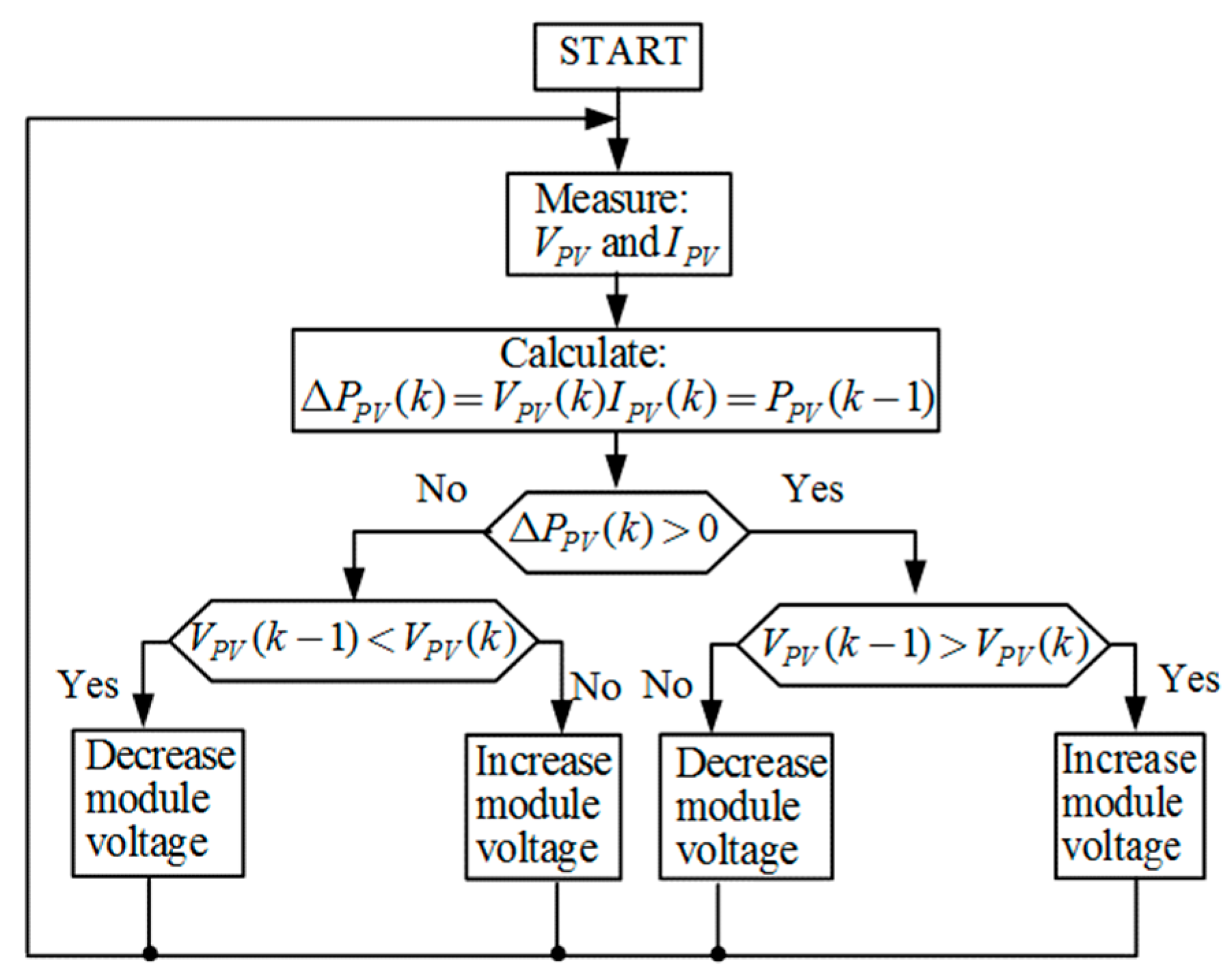
MPPT is a way of controlling a photovoltaic system so that it can obtain as much power as possible from it. The MPPT algorithm monitors output voltages and output currents of solar panels and determines the set point current, such as the reference panel current IPV_ref in which the maximum power is delivered. Many different conventional MPPT techniques have been developed, but those such as disturbance and observation analysis and incremental conductance method are widely used due to their simplicity, even though the energy losses in these methods are higher [
10,
11,
14].
Due to simplicity and fast response, the P&O algorithm was implemented.
Figure 5 shows the block diagram of the P&O MPPT algorithm and its operation algorithm. At a given operating point, the MPPT measures the changes in the output power and voltage of the PV panel. The MPPT algorithm repeats cyclically until the maximum power point is reached, i.e., when dP/dV = 0.
3.2. Dead-Beat Load Current Controller
The load current should always be adequate to the panel current value. A dead-beat load current controller plays a very important role in controlling an inverter load current. A MPPT algorithm determines the set point current in which maximum power is delivered. The input voltage VPV_MPPT and input current IPV_MPPT of the two-phase DC-DC boost converter are the same as determined by the MPPT algorithm. The DC-DC boost converter increases input voltage using the standard two-level control method.
The first level controls the output voltage of the DC-DC boost converter to stabilize the DC-link +VCC voltage, according to the reference voltage Vref.
The second control level regulates the output current IPV* of the DC-DC boost converter by controlling the load current of the inverter. The inverter injects a controlled sinusoidal current into the grid, locked to the phase and frequency of the grid voltage (no reactive power is delivered to the grid).
The active and reactive power of the inverter is controlled using a power calculation algorithm that uses the amplitudes of the first harmonics of the grid voltage and load current as well as the phase angle between these waveforms, measured by the PFD in each period of these waveforms.
Assuming that the input and output power of the DC-DC boost converters are the same as the power delivered to the grid, we receive the following:
where
Vgm,
IOm—the amplitudes of the grid voltage and current, and
M—the modulation index of the PWM modulator.
According to Equation (7), with adaptive control of the inverter output current, we achieve the following:
Dead beat control finds the input to bring the output to a steady state in the least number of time steps
3.3. Clock Selection, Timing and Synchronization Using STM32L476xx Microcontroller
The synchronization system is an essential part of every control system, being responsible for detecting the network signal parameters (amplitude, frequency and phase) used in the control process.
The clock selection and timing of all signal processing blocks are based on the set frequency of the three microcontroller AHB buses:
fosc = 80 MHz [
28]. Three synchronized clocks are used to drive the control blocks with the following frequencies:
- (1)
Rated grid frequency fg = 50 Hz, Tg = 20 ms.
- (2)
For the rated grid frequency fg, the sampling frequency fs = 80 kHz (Ts = 12.5 µs) is used by the analog-to-digital converter (ADC) to sample the grid voltage in each period Tg. With a rated network voltage period of 20 ms, this gives 16,000 samples in each voltage period.
- (3)
Switching frequency of the inverter fc = 40 kHz, Tc = 25 µs (the carrier frequency of the linearized PSCPWM modulator).
Most often the voltage and the load current waveforms of the grid connected inverter are distorted by non-linear loads, sometimes due to changes in frequencies within the electrical distribution systems. The distortion level and THD of the load current largely depends on the actual output power of the inverter [
26].
Accurate measurement of the phase and frequency of the grid voltage in these conditions is difficult to obtain, but crucial for the operation and control of the converter. The PFD frequency detector, detection, and synchronization system, linearized PSCPWM modulator, and power calculation module require sinusoidal waveforms of the grid voltage and load current for proper operation. Therefore, the sampled voltage and current are filtered by digital finite impulse response (FIR) band-pass filters (BPF), producing an output at approximately the first harmonics of the input waveforms. The voltage and current are sampled by galvanic isolation circuits. At low power at the inverter output, when its current is small and strongly distorted, and measuring the phase angle φ_i (t) would be problematic, it was assumed that the phase angle φ_i (t) = 0 when the load current amplitude does not exceed the assumed threshold value I_0m (t) < 0.2 A. The generated reactive power is thus very small and can be neglected.
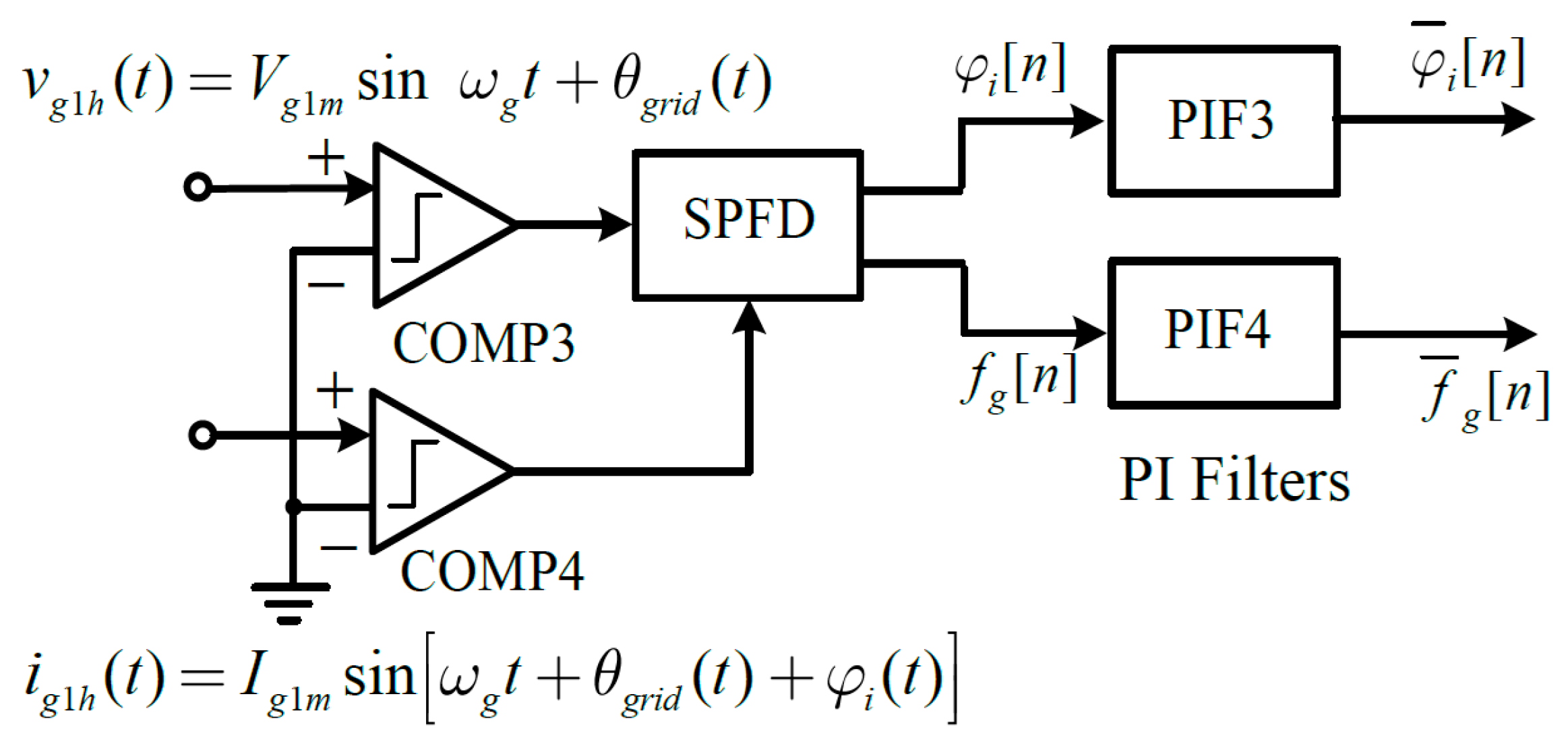
Figure 6 shows the measurement system of the phase angle
between the grid voltage and load current vectors, as well as the grid voltage frequency
, based on a software phase-frequency detector (SPFD) implemented on the STM32L476RGTx microcontroller.
Two comparators, COMP3 and COMP4, were used to transform the sinusoidal waveforms of the first harmonics of the network voltage and load current (obtained as shown in
Figure 4) into square waveform. The SPFD is implemented on the full-featured general-purpose timer TIM4, using CH1 and CH2, and is controlled by the same sampling frequency (
fs = 80 MHz) as all ADCs. Using two independent TIM4 channels for Input Capture and Output Compare, as well as a synchronization circuit to control the timer via external signals, TIM4 interrupts UI1–UI4 and updates events UEV1–UEV4 at the moments of zero-crossing of the first harmonics of the grid voltage and load current, as illustrated in
Figure 7. The TIM4 upcounter in external clock mode configuration can be counted at each rising or falling edge on a selected input. Therefore, sinusoidal waveforms of the first harmonics of the grid voltage and load current were converted to rectangular ones using comparators.
Since the grid frequency can vary in the range from 49 Hz to 51 Hz, the sampling frequency fs is tuned in each period of the grid voltage in such a way as to obtain 1600 samples in each subsequent period Tg[n] of the grid voltage. (The twice-lower switching frequency fc of the linearized PSCPWM modulator is also tuned in a similar way to obtain 800 samples in each period of the grid voltage).
The following data are calculated in each subsequent period of the grid voltage:
- (1)
Period and frequency of the grid voltage, given as follows:
- (2)
The phase angle between the grid voltage and load current vectors, as follows:
where
—sampling frequency use in the
n-th period of the grid voltage (the same as used by the PLL in the synchronization block),
and
—the numbers of counted pulses with the frequency
. The calculated values of
and
are then filtered by two proportional-integrating PIF3 and PIF4 filters with finite impulse response, giving averaged values at the outputs with reduced noise and errors.
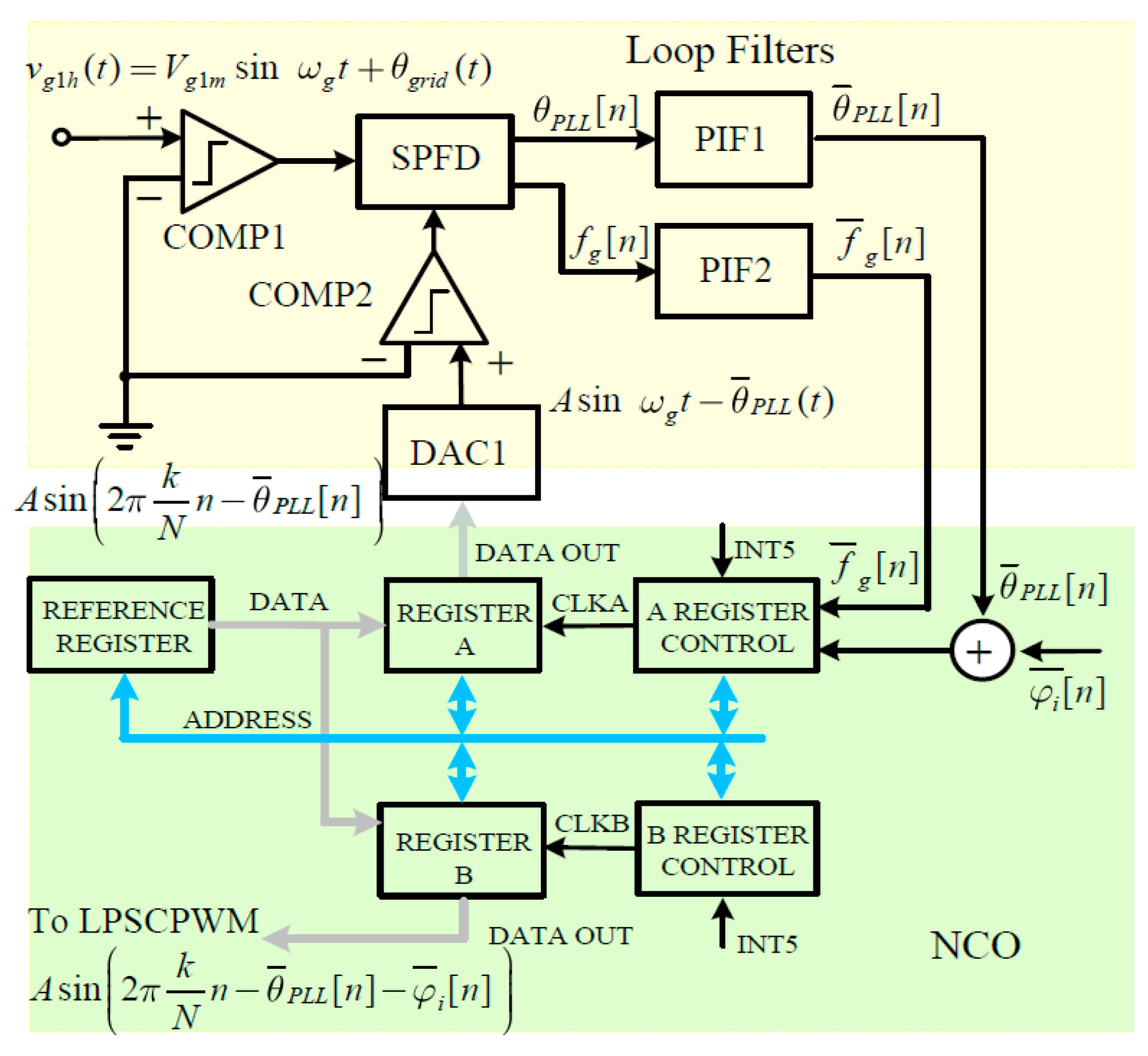
Figure 8 shows the block diagram of the detection and synchronization unit, using a software PLL implemented on the base STM32L476RGTx microcontroller and its peripherals. SPLL is a closed-loop feedback circuit, where the internal oscillator maintains the time and phase of an external periodic signal. This non-linear circuit consists of several main parts: a software phase frequency detector (SPD) (controlling the phase error between the mains voltage and the VCO oscillator voltage), a loop filter (LF), a PID controller (minimizing the error and determining the PLL dynamics), and a VCO that recreates the estimated signal. For SPLL, the VCO is tunable by a numerically controlled oscillator (NCO).
The SPFD in
Figure 8 is implemented in the same way as previously described in
Figure 6, this time using advanced-control timer TIM3 and two internal comparators COMP1, COPM2. Using two independent channels for Input Capture and Output Compare as well as a synchronization circuit to control the timer via external signals, timer TIM3 interrupts UI5–UI8 and updates events UEV5–UEV8 at the moment of zero-crossing of the two sinusoidal waveforms.
Two cases of the phase angle between the grid voltage first harmonic and the voltage generated by the PLL for (a)
> 0 and (b)
< 0 can be illustrated in the same way as in
Figure 7.
Two proportional-integrating PIF1 and PIF2 filters with finite impulse response give averaged values of the and at their outputs, set dynamic PLL performance limits, and help filter out the generated noise.
The sampling frequency
is tuned to obtain 1600 samples in each subsequent period
of the grid voltage, and the following data are calculated:
where
and
—the numbers of counted pulses with the frequency
fs[
n].
The numerically controlled oscillator (NCO), i.e., a sine wave generator that changes phase depending on the numerical input signal, was implemented in the form of a synchronous register A with a capacity of 1600 cells.
At the beginning of each period of the grid voltage
(in response to the INT5 interrupt), 1600 selected samples from the reference register are copied to the A register, with all selected samples already shifted in phase by the calculated angle
(Equation (6)). The reference register with a capacity of 2400 cells contains samples of the ideal reference sinusoidal voltage sin[(2π/1600)/
n] with a frequency of 50 Hz, sampled at a frequency of 80 kHz in the range given below:
where
n = −399, −398, …−1, 0, 1, 2, …, 1598, 1599, 1600, 1601, …, 1698, 1699.
If the address of the reference cell for n = 0 is ADD0, then the addresses of the 1600 shifted in phase cells by the calculated angle start at address ADD0 . Since the clock frequency that writes selected samples from the reference register to the A register is tuned to the grid frequency, even when this frequency changes, there are always 1600 samples for the full grid period.
In a similar way, samples from the reference register are also copied to register B; however, all samples are shifted by the phase angle .
The B register contains 1600 samples of nine-bit numerical sine wave, oversampled by twice the required sampling frequency, at the switching frequency of 40 kHz.
which is a modulating signal for the linearized PSCPWM digital modulator.
The anti-island detection can be easily applied and implemented by extending the described PLL system. The active frequency drift (AFD) method may be used for this purpose; this is widely described in [
14,
15,
16]. The method is based on injection into the Point Common Coupling (PCC) of the current, with slightly distorted frequency.
When the grid is disconnected, a phase error occurs between the current and voltage in the PCC. After detecting this error, the inverter tries to compensate it—the frequency of the generated current increases until the frequency exceeds the limits and is detected by the OFP/UFP [
16].
3.4. Nine-Bit Linearized PSCPWM Modulator
Digital nine-bit linear PSCPWM modulation was implemented using STM32L476xx microcontroller and its peripherals, based on the counter method. Linearized PSCPWM is equivalent to the optimal analog PSCPWM modulation scheme with the connections of analog segments of modulating segments by straight sections [
21,
29].
The 9-bit numerical sine wave defined by Equation (7) and stored in register B (
Figure 8) is directly converted into a 32-bit linearized PSCPWM data and then requantized into 9-bit digital outputs. Then, the quantized nine-bit start and end times of the pulse edges are converted by a digital-to-time converter (DTC) into two physical trains of one-bit PWMA and PWMB signals. These signals are sent outside the microcontroller to the extended linearized PSCPWM modulator. The extended linearized PSCPWM modulator generates all necessary signals to control the IGBTs of the inverters.
A detailed description of the construction and operation of the linearized PSCPWM modulator, including the times of the initial and final position of the pulse edge in each switching cycle calculated using the linearized method, can be found in [
30].
4. PSPICE Simulation and Measurement Results
The proposed inverter has been implemented on IKW50N60DTP fast IGBT transistors, Schottky diodes STPSC20065D, assuming that the load power is up to 4 kW, the output voltage of the string PV panel is 195 V, the DC-link voltage VCC = 380 V, the reference grid frequency fg = 50 Hz, and the switching frequency fc = 40 kHz. Inverter systems were tested in the PSPICE program with the same components, as well as the same simulation parameters.
To control the IGBT switches, dual-channel, isolated, and fast MOSFET gate drivers 2EDF7175F were used. These circuits have a dual supply VDD=5 V on the input side and on the output side, VDDA and VDDB, which are supplied from separate isolated power supplies (
Figure 3). Each of the
VDDA and
VDDB voltages is generated by a standard MGJ2D151505MPC DC-DC converter with a primary voltage of 15 V isolated from secondary voltages of +15 V and −5 V. Output voltages +15 V and −5 V allow the IGBT gate to be charged to +14 V and discharged to −4 V during each switching cycle, ensuring the optimal drive level for best system performance. Grid voltage
Vg = 230 V ± 10%; Capacitancs:
C1 =
C2 =
C3 =
C4 = 1 mF; Filter inductors:
L1 =
L2 = 0.5 mH; Filter Capacitor:
CO = 1 µF; PV parasitic capacitance:
CPVg = 0.2 µF; Boost converter inductors:
L = 0.5 mH. All relationships between voltages, currents, and powers at the input and output of the inverter were simulated by connecting the inverter output to the load resistor.
Figure 9 shows a comparison of the input and output power characteristics and the efficiency versus the load resistance of the DC-DC boost converter implemented in two versions: single-phase (
Figure 9a), and two-phase (
Figure 9b).
The simulations of the characteristics were made in the PSPICE at the output voltage of the string PV panel 195 V, DC-link voltage VCC = 380 V and the switching frequency of 40 kHz. The two-phase converter provides higher efficiency and lower output voltage ripple than the single-phase converter, especially when processing higher output power, as shown below:
- −
Single-phase converter: 97.75% < η < 98.66%, for 3250 W > PO > 800 W;
- −
Two-phase converter: 98.45% < η < 98.68%, for 3250 W > PO > 800 W.
Therefore, a two-phase converter with the same electronic components as in the simulation was implemented in practice.
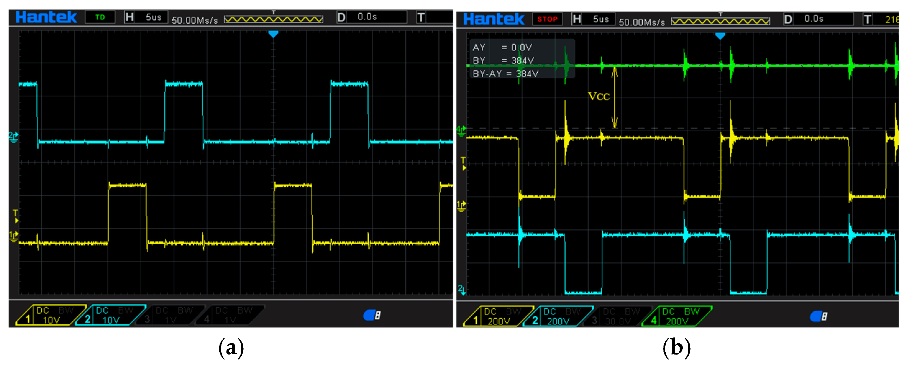
The assembled two-phase DC-DC boost converter with PCBs on the test bench is shown in
Figure 10, while the oscillograms of the PWM control signals on the T
9 and T
10 gates, as well as the voltages on the collectors of these transistors and the DC voltage at the converter output, are shown in
Figure 11. Oscillograms were taken at the output voltage of the string PV panel 195 V, with a DC-link voltage
VCC = 380 V, and a switching frequency of 40 kHz.
The measured input and output power characteristics and efficiency as a function of the load resistance of the tested boost converter are quite similar to those simulated in PSPICE, which are shown in
Figure 9b.
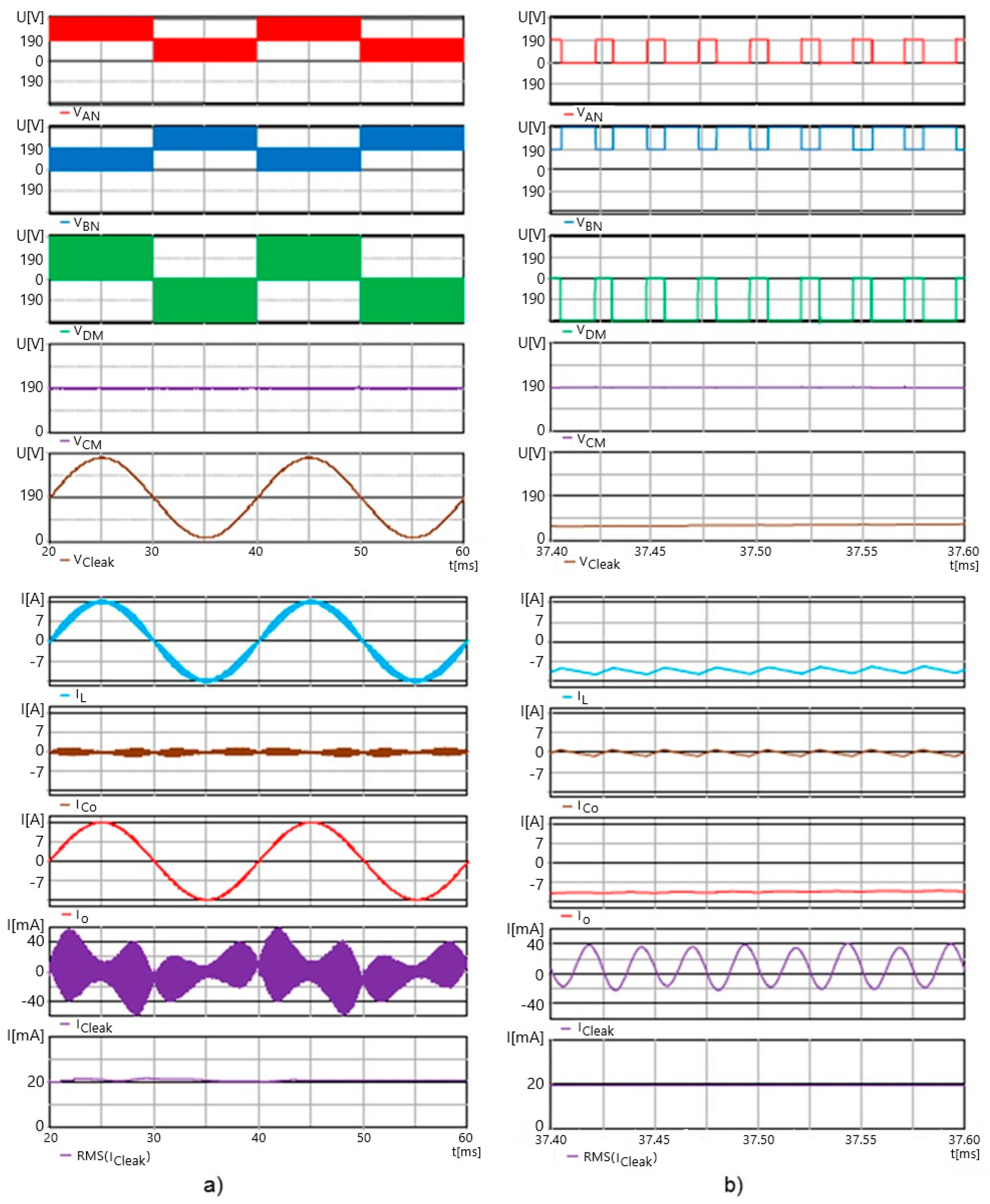
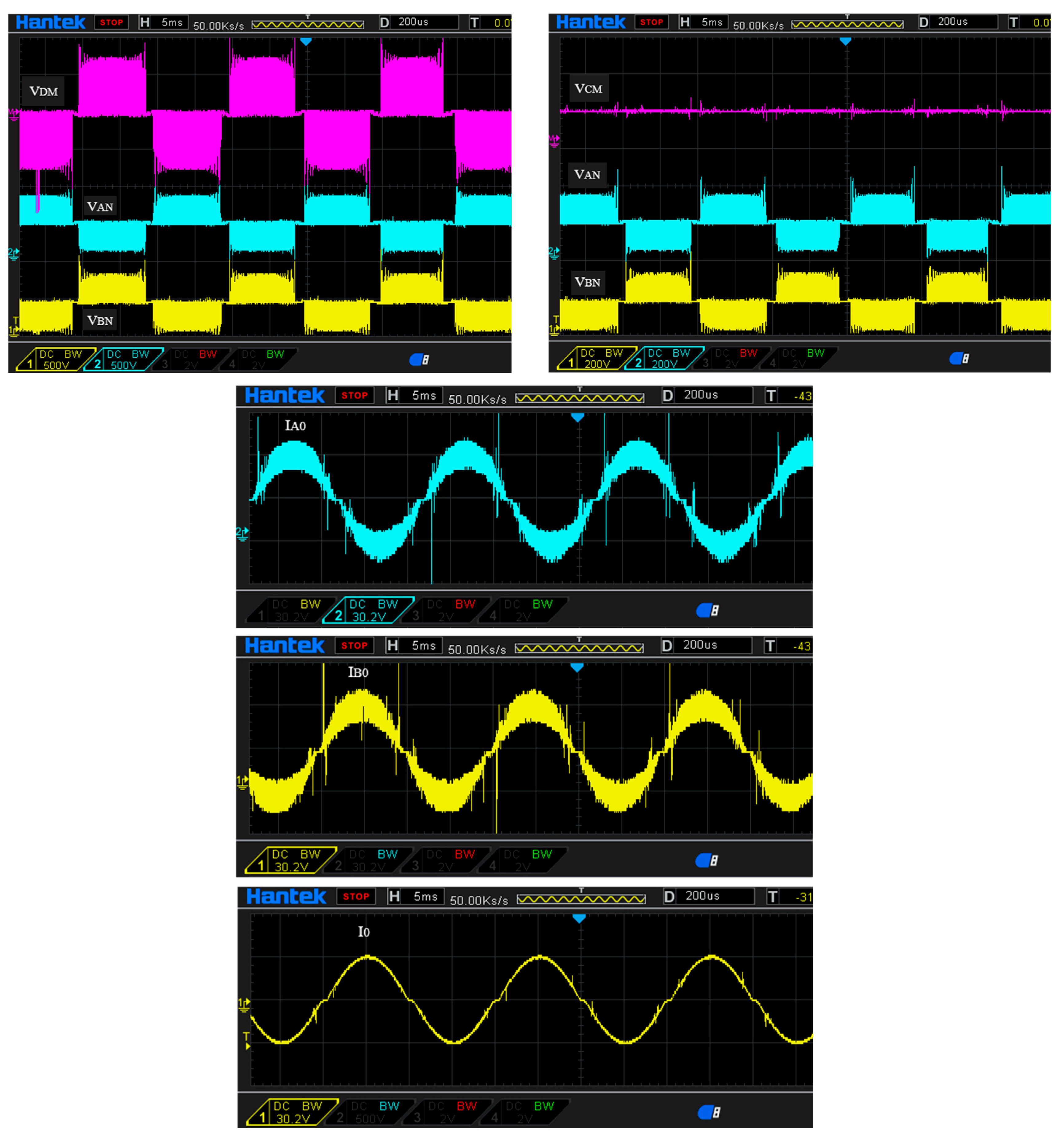
The PSPICE-simulated output voltages and currents of the S-PT inverter are shown in
Figure 12a. As can be seen, the simulated voltages and currents in PSPICE are almost the same as the idealized waveforms in
Figure 2b. However, although CMV has a constant value
VCC =
VCC/2 = 190 V, an additional sinusoidal leakage current of almost 30 mA RMS flows though the leakage capacitance
CPVg.
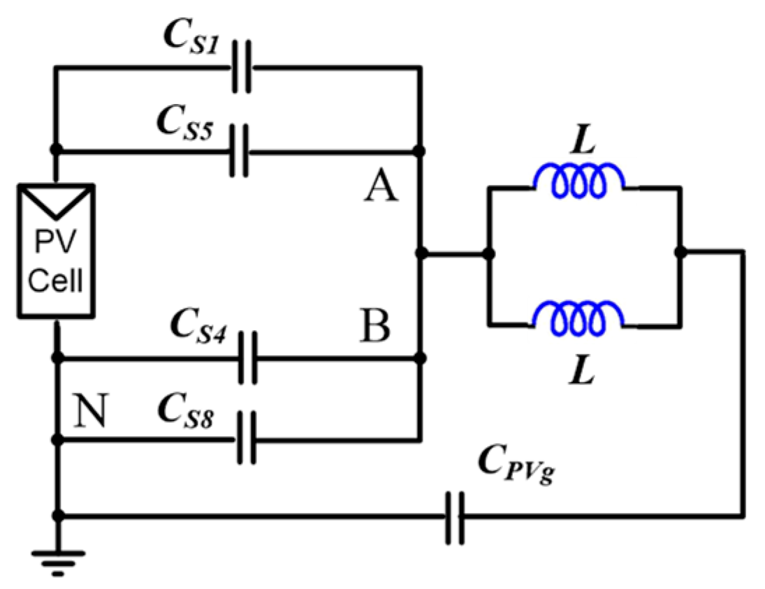
The effective value of the leakage current was calculated for the entire period of the mains voltage. The leakage current is the result of the overcharging of the IGBT junction capacitances during their switching and is also generated in other full-bridge and clamped inverter configurations, such as H5, H6, and HERIC [
2]. When switching the IGBT from the free state to the active state with a positive or negative half-period, an additional resonance path is created (shown in
Figure 13), in which the IGBT junction capacitances CTj are overcharged.
The resonant frequency can be calculated from the following formula:
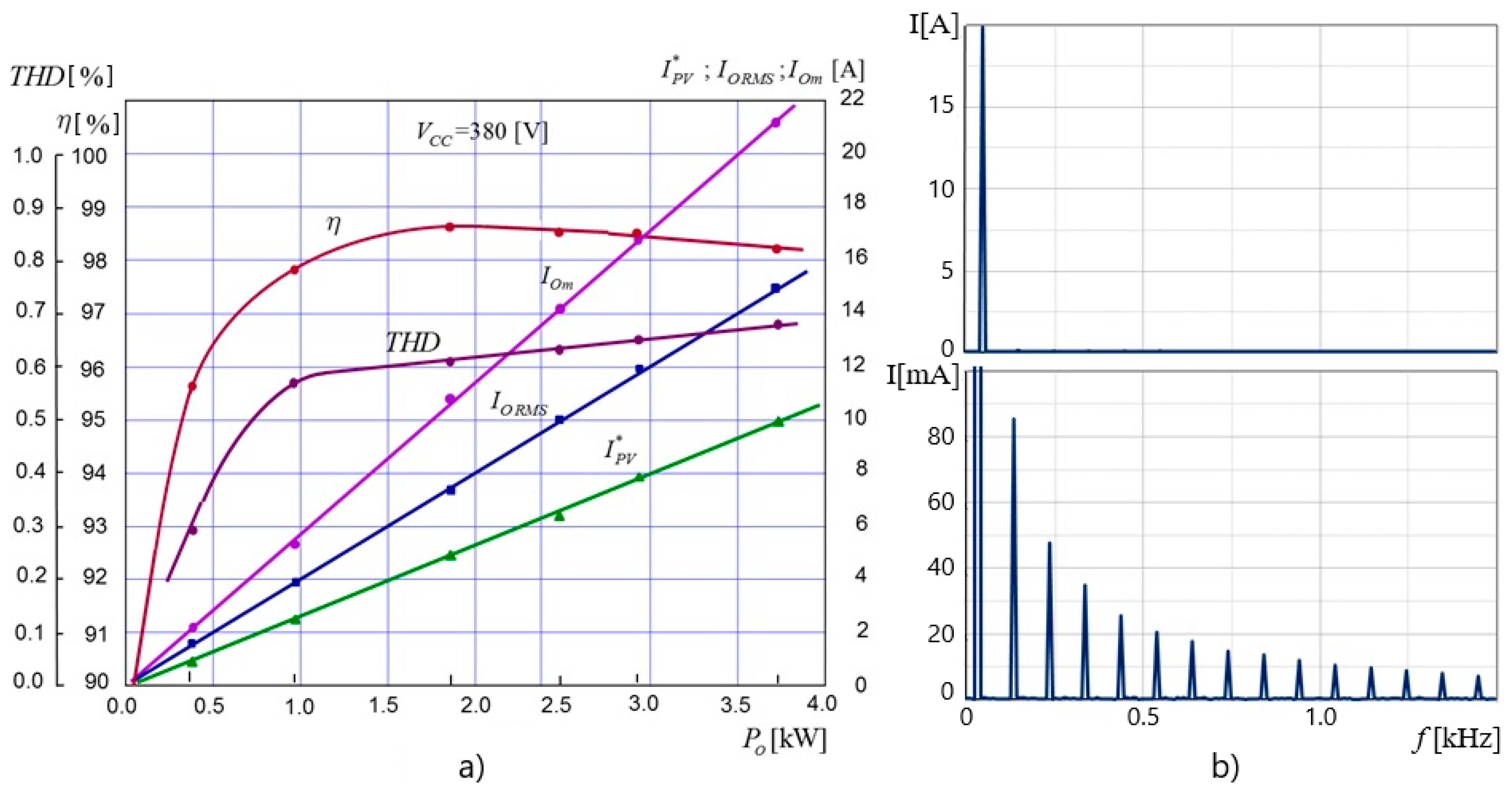
Figure 14 shows the dependence of the efficiency and THD coefficient of the S-PT inverter on the output power PO, with a deviation of +5% from the rated value of the mains voltage given as RMS Vg = 230 V.
Optimal control of the IGBTs results in significant limitation of the shoot-through currents during the transistor switching and reduction in both conduction and switching losses, ensuring the high efficiency of the inverter.
Similarly to analog PSCPWM modulation, the digital linearized PSCPWM signal also has very attractive spectral characteristics; this is because the frequency spectrum has no harmonics of the switching frequency, and no intermodulation components around odd multiples of the switching frequency, which greatly facilitates the filtering of the DM voltage at the output of the inverter. However, the output current of the inverter exhibits slight non-linear distortions, which are mainly caused by delaying the turn-on time of the IGBTs in order to limit the shoot-through currents. In the entire range of output power variability, the THD determined on the basis of the analysis of the load current frequency spectrum is less than 0.68%.
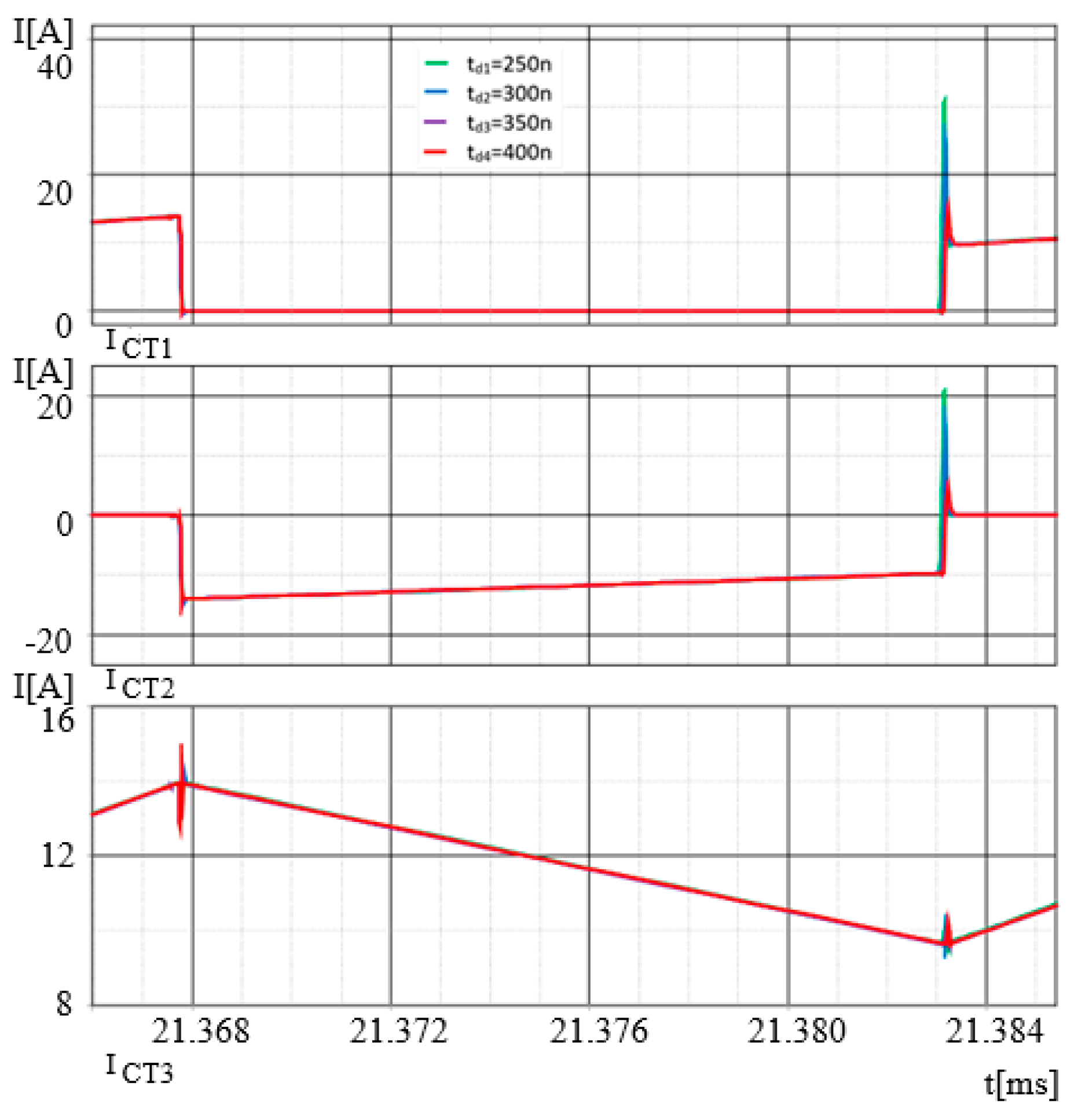
Figure 15 shows the time simulations of the IGBT collector currents, namely ICT1, ICT2, and ICT3, when switching a load current of approximately
IO = 14 A in the selected switching period.
The falling edge of the control signal S1 turns T1 off and T2 on, and the reverse current ICT2 flows. In the case of the rising edge of S1, T1 is turned on at the forward current ICT1, and T2 is turned off. T3 is always turned on during these selected switching periods. As shown in
Figure 15, the optimal delay time td4 = 400 ns for the IGBT turn-on gives a significant reduction in breakdown currents.
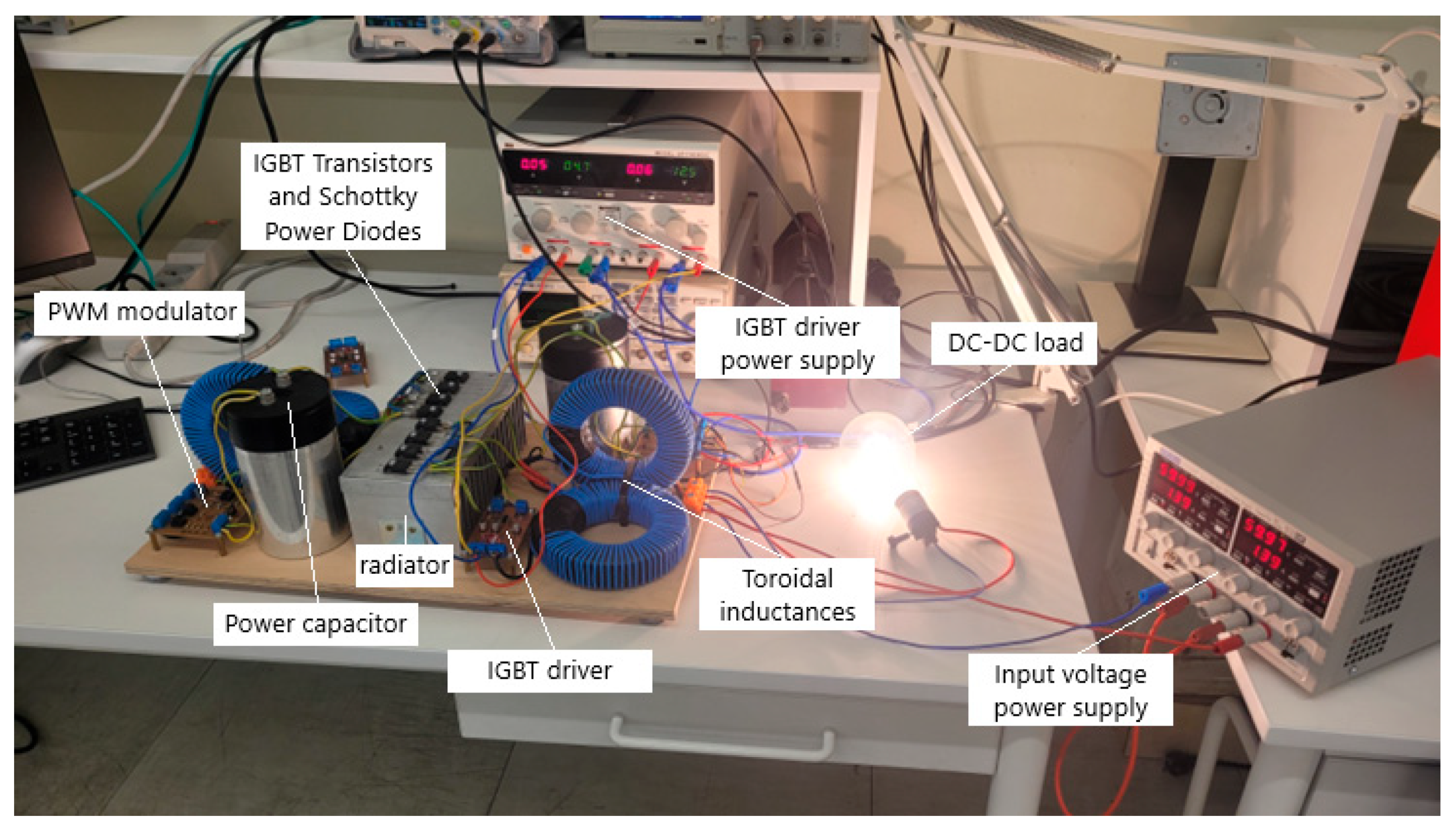
Figure 16 shows a photograph of the assembled S-PT inverter in three-level CHB configuration. Load resistance is connected to the inverter output via short cables from the outside.
Figure 17 shows oscillograms of the
S1 and
S2 control signals generated on the basis of
PWMR and
PWML signals by the digital nine-bit linearized PSCPWM modulator with extended architecture.
Figure 17a presents the following signals from top to bottom:
Vm—grid voltage,
PWMA,
PWMB,
S1,
S2, generated in two grid voltage periods, while
Figure 17b shows zoomed views of these signals in selected small fragments, respectively, for positive (b) and negative (c) half-periods. It can be seen that
S1 =
PWMA ·
PWMB and
S2 =
PWMA +
PWMB, respectively.
Figure 18 shows the measurement waveforms at the output of the S-PT inverter, measured at a DC-link voltage of
VCC = 380 V, a switching frequency of 40 kHz, and a load resistance of R
O = 64 Ω.
Measured time waveforms of the voltages and currents are similar to those obtained in PSPICE simulations, but overvoltage spikes appear in the IGBT switching processes.
The measured energy dependencies for various load resistances and the energy efficiencies of the S-PT inverter determined on their basis are presented in
Table 1. The obtained results are comparable to those obtained in PSPICE simulations, which are presented in
Figure 9.
Phase angle information of the power grid and full synchronization of the output voltage with the grid are critical for the operation of the PV converter. Implemented on the STM32L476RGTx microcontroller phase frequency detector (SPFD) from
Figure 6, at a sampling frequency of 80 kHz, i.e., 1600 samples per one period of the grid voltage, allows for the measurement of the phase angle between the grid voltage and load current vectors with very high accuracy, with a resolution of 360°/1600 = 0.225°.
Figure 19 shows the oscillograms of the voltages generated at the output of the implemented digital PLL from
Figure 8 in the transient state when synchronization is achieved, with a step-phase excitation at the input of ±45°.
Similar oscillograms with a step frequency excitation from 50 Hz to 51 Hz and from 50 Hz to 49 Hz are presented in
Figure 20.
SPLL achieves synchronization in less than 4 periods of the grid voltage with a step-phase excitation of ±45° and three periods with a step frequency excitation of 50 Hz ± 1 Hz [
20].
The following set of equipment was used to test the inverter:
- −
Rigol DG1022Z 25 MHz 200 MSa/s, function generator (Rigol, Beijing, China);
- −
HP 8593 Agilent spectrum analyzer (Agilent, Santa Clara, CA, USA);
- −
Hantek DO4254B 250 MHz, 4 channel advanced digital oscilloscope (Hantek, Qingdao, China);
- −
Pico Technology PicoScope 2206A (St Neots, UK);
- −
EA-PS 3200-10 C (Elektro-Automatik, Viersen, Germany) 0–200 V, laboratory power supply;
- −
DF1432005C, 2 × 30 V/5 A, (3–6 V)/1 A, (8–15 V)/3 A, laboratory power supply.
5. Conclusions
The article presents an original single-phase transformerless three-level photovoltaic inverter in the cascade H bridge configuration, powered by two series voltage sources with a voltage twice lower than the DC-link voltage. The midpoint potential of these sources provides a natural zero-voltage reference level against which the output PWM waveforms are generated, ensuring a constant CM voltage level and zero leakage current. In addition, the voltage stress on all switches, diodes, and gate control circuits is half of the DC-link voltage.
Proposed topology in a cascading H-bridge configuration contains eight bi-directional switches, whereby current in active mode flows through three switches. Comparing the proposed topology to the most effective derived family of HERIC-based clamping inverters, the cost and the conduction losses of the proposed topology may increase a little, because it has one switch more, as well as the fact that the current in active mode flows through three, not two, switches.
However, the topology of the S-PT inverter in the CHB configuration is unique in that it can be most easily applied to the construction of three-phase transformerless three-level PV inverters with zero CM voltage and no leakage current. For this purpose, one of the branches of the S-PT inverter in the CHB configuration should be duplicated three times (n-times in the case of an n-phase inverter), and power these three parallel branches by two complementary ±VCC voltage sources. The midpoint potential of these sources constitutes a natural reference level during zero-voltage mode against which the PWM waveforms are generated during the other two operating modes. The grid neutral line is directly connected to the negative terminal of the PV panels and neutral point N. The control signals S1 and S2 are active in individual branches of the three-phase inverter only during the time 2π/3 intervals between the natural commutation points of the inverter.
An appropriate DC-link voltage VCC = 380 V is generated by a typical two-phase DC-DC boost converter, fed from the string PV panel with output voltage of 195 V. The DC-DC boost converter increases input voltage according to the MPPT algorithm, stabilizes the DC-link voltage VCC, and controls the output current. A high efficiency of 98.45% < η < 98.68%, for 3250 W > PO > 800 W, and low output voltage ripple are achieved with the switching frequency of 40 kHz, while the passive components of the boost converter 2 × C = 1 mF, 2 × L = 0.5 mH, as well as capacitors 2 × 1 mF of the divider, creating two symmetrical sources with half voltage VCC/2, significantly increase the overall system volume and cost.
A multifunctional control system based on STM32L476xx microcontroller was developed to improve power quality and grid stability, as well as to provide safe operation of loads and stable integration of the proposed S-PT inverter in CHB configuration into the grid.
An implementation of a complete optimal gate control system with galvanic isolation for all IGBTs, with detailed descriptions, has been presented.
The presented S-PT inverter has the ability to actively regulate the output voltage and current by responding to relevant output voltage measurements, changing the active and reactive power transmitted to the grid, as well as tracking the phase angle, grid voltage amplitude, and frequency in order to protect against extreme changes in these values.
Grid synchronization technique plays a vital role in maintaining the grid’s power quality and grid voltage frequency requirements. For this purpose, the original measurement system of the phase angle was designed and experimentally verified between the grid voltage and load current vectors, as was the grid voltage frequency fg[n], based on a software phase-frequency detector (SPFD), as well as synchronization unit, using a software PLL, both implemented on the STM32L476RGTx microcontroller.
The SPLL generates in each grid period a modulating signal for the linearized PSCPWM digital modulator in the form of 1600 samples of nine-bit numerical sine wave, oversampled by twice the required sampling frequency at the switching frequency of 40 kHz, synchronous with the grid voltage, but shifted by the phase angle −( + ), ensuring reactive power compensation.
The proposed detection and synchronization units combined with the linearized PSCPWM linear digital modulator guarantee very high accuracy and excellent dynamic parameters, enable synchronization and the safe operation of loads, and enable active regulation of the output voltage and current by controlling voltage measurements or changing the power transmitted to the network.


 ,
, 


