Article

A 12-bit 100 MSPS Full-Swing Current-Steering Digital-to-Analog Converter with Half-Power Supply Calibration Technique

Department of System Semiconductor, Dongguk University, Seoul 04620, Republic of Korea
*
Author to whom correspondence should be addressed.
Electronics 2025, 14(19), 3955; https://doi.org/10.3390/electronics14193955
Submission received: 8 September 2025 / Revised: 5 October 2025 / Accepted: 6 October 2025 / Published: 8 October 2025

Abstract

We present a digital-to-analog converter (DAC) with full-swing DAC output and a proposed half-power supply calibration technique. To generate a full-swing DAC output, symmetric thermometer decoders and an output selector are implemented to select the appropriate current cell according to the output voltage range. Furthermore, to improve the linearity, we propose a half-power supply calibration circuit consisting of comparators and calibration counters to control the current of the current cells at the half-power supply voltage point, where the voltage mismatch typically occurs. The DAC was fabricated in a 28 nm CMOS process, with a full chip area of 0.95 mm × 0.93 mm. The measurement results demonstrate a maximum voltage mismatch improvement of 95% when using the proposed half-power supply calibration technique, with DNL and INL values of 0.39 and 1.15 LSB. The total power consumption was 73.8 mW at 100 MSPS, with analog and digital supply voltages of 1.8 and 1.0 V, respectively.

1. Introduction

With the growing importance of system-on-chip circuits, technological advancements have shifted toward the integration of digital and analog blocks on the same chip. Consequently, the significance of digital-to-analog converters (DACs) facilitating the interface between digital and analog blocks has dramatically increased. DACs are used in various fields, such as in display drivers and medical applications [1,2,3,4,5,6,7,8], and can be generally categorized into two types: voltage- and current-steering. In the case of voltage-steering DACs, the output voltage is generated through an operational amplifier (op-amp), with a high-performance op-amp required to obtain optimal performance. Additionally, these DACs require 2N resistors to achieve N-bit resolution, resulting in a substantial increase in the required chip area as the resolution increases. Therefore, voltage-steering DACs are not considered suitable for high-speed and high-resolution applications. On the other hand, current-steering DACs can operate at extremely high speeds as they generate an output voltage by allowing current to flow through termination resistors, eliminating the need for additional resistor strings. However, due to the use of termination resistors, a voltage drop occurs at the output current cell which, in turn, prevents a full-swing output. Consequently, these DACs are unsuitable for analog applications requiring rail-to-rail output voltage capability, such as display drivers [6].
Moreover, due to the trend toward the miniaturization of electronic devices and the high integration of semiconductor circuits, significant progress has been made in component miniaturization and the development of low-power circuits. Therefore, a decrease in power supply voltage (VDD) has become inevitable. As a reduced VDD leads to a decrease in the available voltage output range that can be utilized in current-steering DACs, the voltage corresponding to the least significant bit (1LSB) decreases as the resolution increases. This reduction in the 1LSB ultimately negatively affects the differential nonlinearity (DNL) and integral nonlinearity (INL) of the DAC, degrading its linearity characteristics. Therefore, to design a DAC with full-swing output, nMOS and pMOS were selectively chosen for the development of current cells. In addition, to improve the DAC’s linearity, a compensation circuit is added to calibrate the half-point and control the current of the current cells.
The remainder of this paper is structured as follows. Section 2 discusses the proposed DAC structure, including the circuit design and implementation. Section 3 describes the fabricated chip and the measurement environment, followed by an analysis of the measurement results using various evaluation metrics. The conclusion is presented in Section 4.

2. Proposed DAC Structure

Figure 1 shows the main blocks of the proposed DAC. The 12-bit input signal is sequentially divided into three segments comprising 4 bits, 4 bits, and 5 bits, including a 1-bit margin, with the remaining bits excluding the MSB (most significant bit), which is used to generate a symmetric signal based on half of the VDD. To ensure uniform timing, these segmented input signals are adjusted using an input buffer to have the same delay time. Subsequently, as it passes through each thermometer decoder, the input signal—which is a binary code—is converted into a thermometer code. In this process, the thermometer decoders integrate latches, eliminating the need for additional latches and reducing the overall chip area. After converting the output thermometer code into the analog domain through a level shifter, the timing of the input is adjusted through a quaternary driver to reduce the glitch of the current cell. Using the input with adjusted signal timing, the current generated in the current cell is converted into voltage through termination resistors. In this way, a DAC with full-swing output range is designed by selecting the output from either the nMOS or pMOS current cell based on the desired output voltage range, using an output selector comprising a multiplexer. Due to the current-steering design of this DAC, it can operate at high speed and does not require an additional resistive string for analog voltage conversion. Furthermore, its thermometer encoder structure yields low INL and DNL errors, along with excellent monotonicity characteristics.

2.1. Switching Logic and Symmetric Thermometer Decoder

Figure 2a illustrates the circuit structure of the switching logic for the digital block presented in this paper, which possesses a binary decision diagram (BDD) structure. When using the BDD structure, the full swing of the output voltage of the switching logic is not attainable as the operation proceeds with the nMOS only. Therefore, the level restoration circuit (LRC) comprising the pMOS is connected in a cascode configuration. The LRC can perform not only level restoration, but also enables a deglitching operation by adjusting the switching point of the switching logic output. Furthermore, the nMOS, which operates in response to a clock signal (clk), is connected via a cascode between the LRC and the BDD to enable a latch operation within the switching logic itself. Using this structure, an additional deglitching circuit or latch is not required, thereby reducing the chip area. Additionally, as the BDD structure does not use the pMOS, the area and power consumption of the digital block can be reduced.
As the current cell to output at VDD/2 should be selected in the DAC proposed in this paper, the cells should output symmetrically at this point. Therefore, as shown in Figure 2b, we designed a decoder that outputs thermometer code symmetrically as the binary input increases. As shown in Figure 2b, taking the 4-bit binary code (B3 to B0) as an example, when the MSB is 0, it can be observed that the thermometer code (T0 to T6) increases sequentially as the binary code progresses from 0000 to 1111. However, if the MSB is 1, the thermometer code sequentially decreases as the binary code increases from 0000 to 1111. When the current cell is driven using this thermometer code, the output is symmetric according to the MSB. The combined latch and thermometer decoder operates with a latch clock frequency of 100 MHz, and the typical propagation delay of the decoder is approximately 110 ps. These values were selected to ensure proper timing alignment and to minimize glitch energy during switching.

2.2. Current Cells

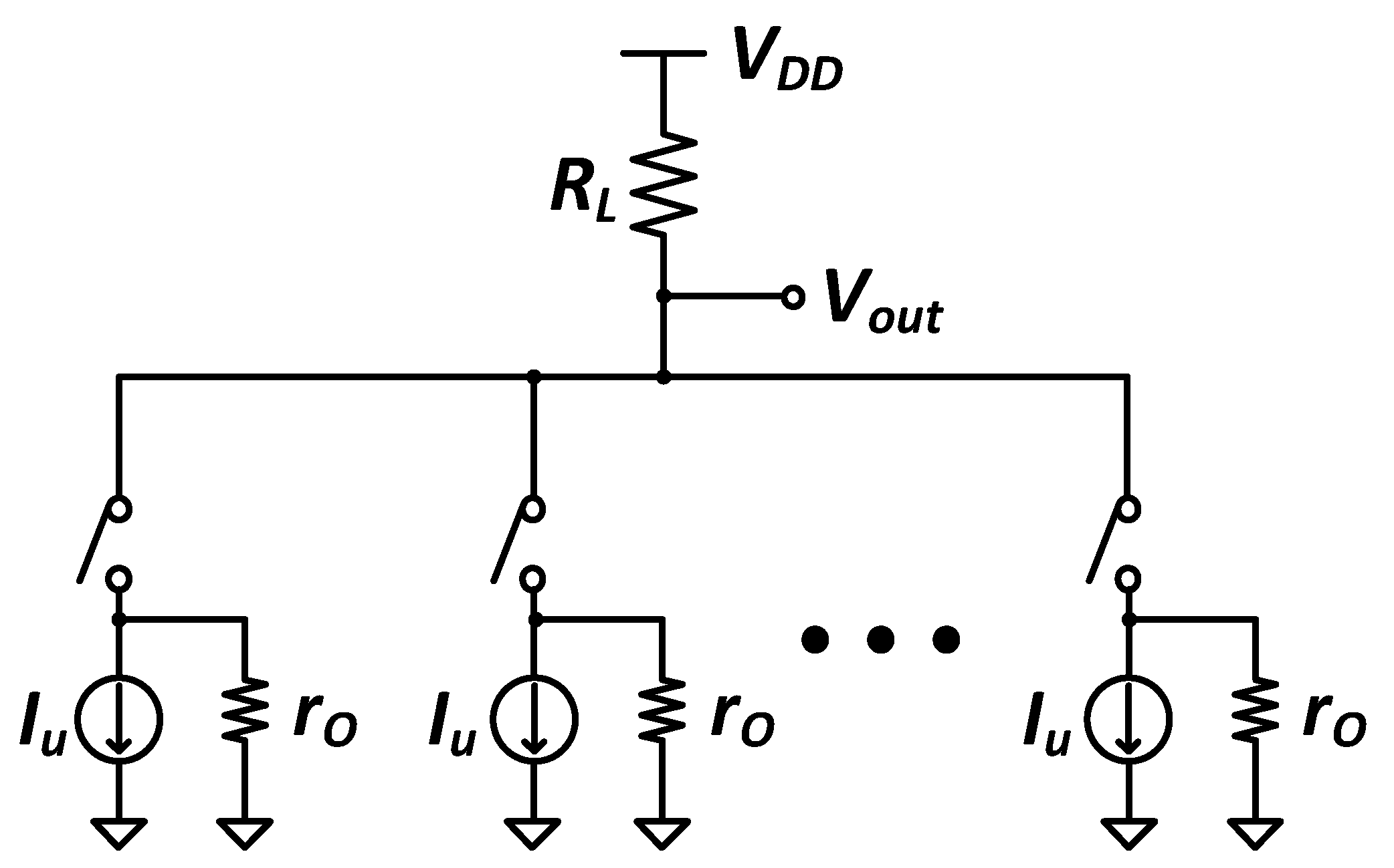
As the performance of a current-steering DAC depends on the performance of its current cells, several factors should be considered when designing the current cells. First, considering that it has a finite output impedance (ro), the equivalent circuit of a current cell is shown in Figure 3.
When M current cells are in operation, the actual resistance across the DAC output, Reff, and the DAC output voltage, Vout, can be expressed as follows:
R e f f = R L | | ( r O / M )
V o u t = I u [ R L | | r O / M ]
where RL represents the terminal resistance for current conversion and Iu represents the unit current flowing through the terminal resistance. The DAC output voltage changes depending on the output impedance of the current cell and, as the number of current cells connected to the output terminal increases, the effective resistance (Reff) decreases. This affects the INL performance of the DAC, and the maximum INL value when M current cells are in operation is calculated as follows:
I N L m a x = I u R L 2 M 2 / ( 4 r O )
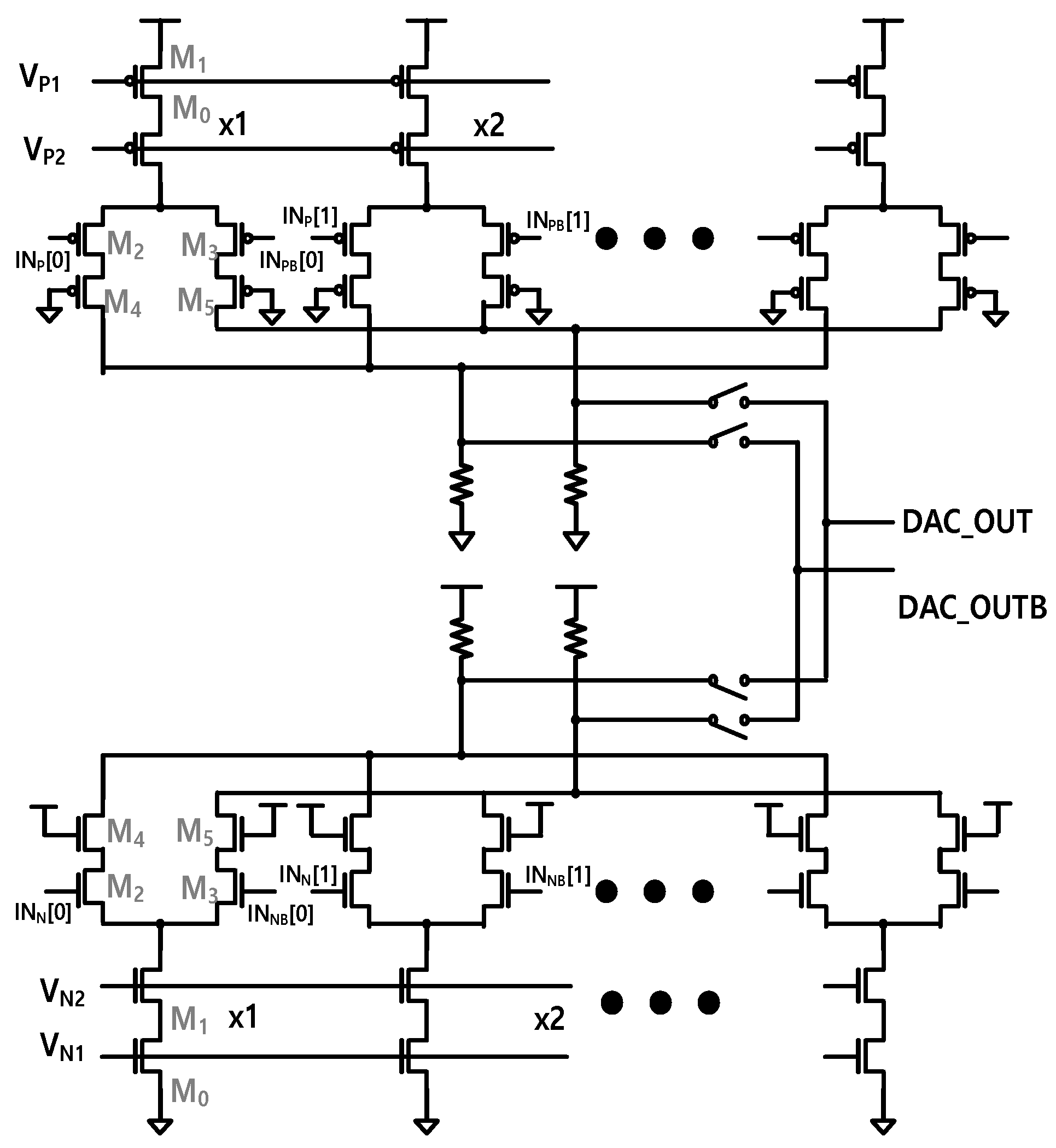
Therefore, to reduce the INL, the output impedance of the current cell should be designed to be large [9]. In addition, when the DAC operates at high speed, abnormal effects, including clock feedthrough, may occur due to the MOSFET switching operation. A current cell with a cascode structure was therefore designed (Figure 4). The output impedance of the current cell was increased using the currentF-source MOSFETs (M0, M1) in a cascode structure. Additionally, by utilizing M1 to separate the switch MOSFETs (M2 and M3) and the current source MOSFET (M0), the effect of clock feedthrough that occurs when operating at high speeds can be reduced. Additionally, by inserting a thick-gate MOSFET between the switch MOSFET and the DAC output, the non-ideal effects of the DAC output stage that may occur due to high-speed switching operations can be mitigated [10,11,12,13,14,15,16]. In this configuration, the pMOS current cell cannot obtain an output up to VDD and the nMOS current cell cannot obtain an output up to GND; thus, the voltage ranges for pMOS and nMOS operations should be secured. Therefore, to design a full-swing DAC, both types of current cells shown in Figure 4 were utilized. As the 12-bit DAC was divided into a 4 + 4 + 5 structure, the W/L design was adjusted such that the current ratio was 512(29):32(25):1. In addition, the output of the pMOS current cell is used from GND to VDD/2, while the output of the nMOS current cell is used from VDD/2 to VDD; in particular, the output of each current cell is selected via the output selection circuit described below.
The detailed results are summarized in Table 1, which lists the W/L dimensions and σ/μ of the currents for both nMOS and pMOS current cells. Monte-Carlo simulations (the number of Monte: 2000) show that the 1-σ current variation (σ/μ) of pMOS current cells ranges from 0.09% to 0.47% depending on the segment current level. For nMOS current cells, σ/μ of currents ranges from 0.12% to 0.45%.

2.3. Quaternary Driver and Output Selector

In the case of a typical current-steering DAC, the circuit comprised a current cell of one MOSFET type (i.e., nMOS or pMOS). However, when only one type of current cell is used, a full-range output swing is not possible due to the operating voltage range of the MOSFET and the voltage drop of the termination resistor, as shown in Figure 5. In other words, an nMOS current cell can only use the output range from VDD to weak ground (GND), while a pMOS current cell can only use the output range from weak VDD to GND. Therefore, to achieve full-range output swing, both nMOS and pMOS current cells should be used. To avoid ambiguity, the valid output ranges can be written explicitly by including the switch on-resistance and the cascode headroom. Let Icell denote the branch current, RL the termination resistor, RSW the equivalent on-resistance along the active switch path, and VSD_p and VDS_n the overdrive voltage to keep the pMOS and nMOS cascode current sources in saturation. For the pMOS cell (lower half range), the output node should satisfy as given by
I c e l l R L + R S W D A C o u t V D D V S D _ p
For the nMOS cell (upper half range), the condition is
V D S _ n D A C o u t V D D I c e l l R S W
Therefore, we select 0–VDD/2 for pMOS and VDD/2–VDD for nMOS that ensures overlapping compliance with margin.
Although the termination resistors inevitably introduce IR drops, the proposed structure minimizes their impact by dividing the operation range into two regions (0–VDD/2 for pMOS and VDD/2–VDD for nMOS). Each current cell thus operates in its most effective region, and a half-supply calibration circuit further compensates for the voltage mismatch at VDD/2. Consequently, the proposed DAC achieves rail-to-rail output while mitigating the limitations caused by the termination resistors.
Additionally, as the performance of a DAC, including its linearity, varies depending on the signal driving the current cell, it is crucial to create a driving signal that is suitable for each current cell [8,9]. However, suppose the same switch signal that drives the current cells is implemented in a structure that uses both current cells. In this case, problems such as considerable glitch energy and errors due to asymmetric switch operations may occur. To address this issue in the proposed full-swing current cell, an additional quaternary driver was designed. As shown in Figure 6a, the quaternary driver is configured as a buffer consisting of two stages of inverters, with four buffers per thermometer code. This configuration enables the generation of two types of current cells and input signals, as well as inverted input signals. In order to reduce the glitch of the current cell, the point where the signals (outp, outpb) for driving the pMOS current cell cross over should be set lower than the Vth of the pMOS current cell switch, and the point where the signals (outn, outnb) for driving the nMOS current cell cross over should be set higher than the Vth of the nMOS current cell switch to operate the current cell (Figure 6b).
The quaternary driver is introduced because the proposed DAC requires simultaneous operation of both pMOS and nMOS current cells to achieve a full-swing output. If conventional binary driver signals were applied to both cell types, asymmetric switching would lead to large glitch energy and degraded linearity. By generating four complementary and non-overlapping signals (outp/outpb for pMOS and outn/outnb for nMOS), the quaternary driver ensures proper timing control, reduces switching glitches, and provides smooth signal transition across the VDD/2 boundary. The driving signal generated by the quaternary driver allows the switching point of the switch of a current cell to be adjusted, thus reducing the glitch occurring in the cell. The quaternary driver generates four complementary and non-overlapping control signals (outp, outpb, outn, outnb). These signals are directly connected to the gate terminals of the switching transistors in the pMOS and nMOS current cells, respectively. In this way, the quaternary driver ensures that each current cell is activated in the correct voltage range (0–VDD/2 for pMOS and VDD/2–VDD for nMOS), while minimizing timing skew and glitch energy during switching.
The signal output by the quaternary driver drives the current cells, with their output selected based on the associated voltage range; that is, depending on the operating voltage range of the MOSFET constituting the current cell, the output of the nMOS current cell is selected from VDD/2 to VDD, while the output of the pMOS current cell is selected from GND to VDD/2. An output selector consisting of a switch is used to implement this operation, as shown in Figure 7. The signal that controls the switch uses the MSB: as shown in Figure 7a, when the MSB is low, the output is smaller than VDD/2 and, so, the pMOS current cell output is output to out, while the nMOS current cell output is output to outb. In contrast, when the MSB is high, the output is higher than VDD/2, and thus, the nMOS current cell output is output to out, while the pMOS current cell output is output to outb.

2.4. Half-Power Supply Calibration Technique

As the two current cells operate independently and produce a full-range DAC output, voltage mismatch occurs at the VDD midpoint, where the two current cell blocks meet. To improve this, the actual VDD/2 voltage and the output of the current cell are compared through a foreground calibration circuit (Figure 8).
First, the input digital code of the DAC is fixed to a value corresponding to VDD/2. Afterwards, the R-string inside the circuit is used to compare the reference voltage (Vref), which has a voltage value of VDD/2, and the output of the current cell through a comparator. At this time, the output voltages of the pMOS and nMOS current cells are set to be higher and lower than Vref, respectively, such that the initial output of the comparator is low. Then, as the calibration circuit operates, the output of the current cell changes. When the output of the pMOS current cell becomes smaller than Vref and the output of the nMOS current cell becomes bigger than Vref, the output of the comparator is flipped.
The output of the comparator serves as an input to the calibration counter. For the initial comparator output, the calibration counter for the pMOS current cell is set to low, while that for the nMOS current cell is set to high. Afterwards, the calibration counter output is sequentially flipped by the comparator output, which is output low. When the comparator output is flipped, the calibration counter operation stops and the calibration counter output is maintained. The output of the calibration counter is fed back to additional control MOSFETs connected to the current mirrors of the pMOS and nMOS current cells. By adjusting the effective bias current of each current mirror, the calibration circuit compensates for the mismatch at VDD/2 until the DAC output is properly aligned with the reference voltage. This feedback mechanism ensures smooth continuity between the two operating regions and reinforces the full-swing performance. Due to the initial calibration counter value, this additional MOSFET does not operate at this time. As the calibration counter operates and its output is sequentially flipped, the additional MOSFET also operates sequentially and the CM current decreases. As a result, the current of the current cell also decreases and the voltage changes. As the calibration operation progresses, the output of the pMOS current cell decreases to a value smaller than Vref. Conversely, when the output of the nMOS current cell exceeds Vref, the operation of the calibration circuit ceases and the cell’s current value is maintained. It should be noted that the comparator in the half-power supply calibration circuit has an offset voltage of less than ±3 mV, which is sufficient to cover the DAC’s output range and to ensure accurate compensation at VDD/2.

3. Experimental Results

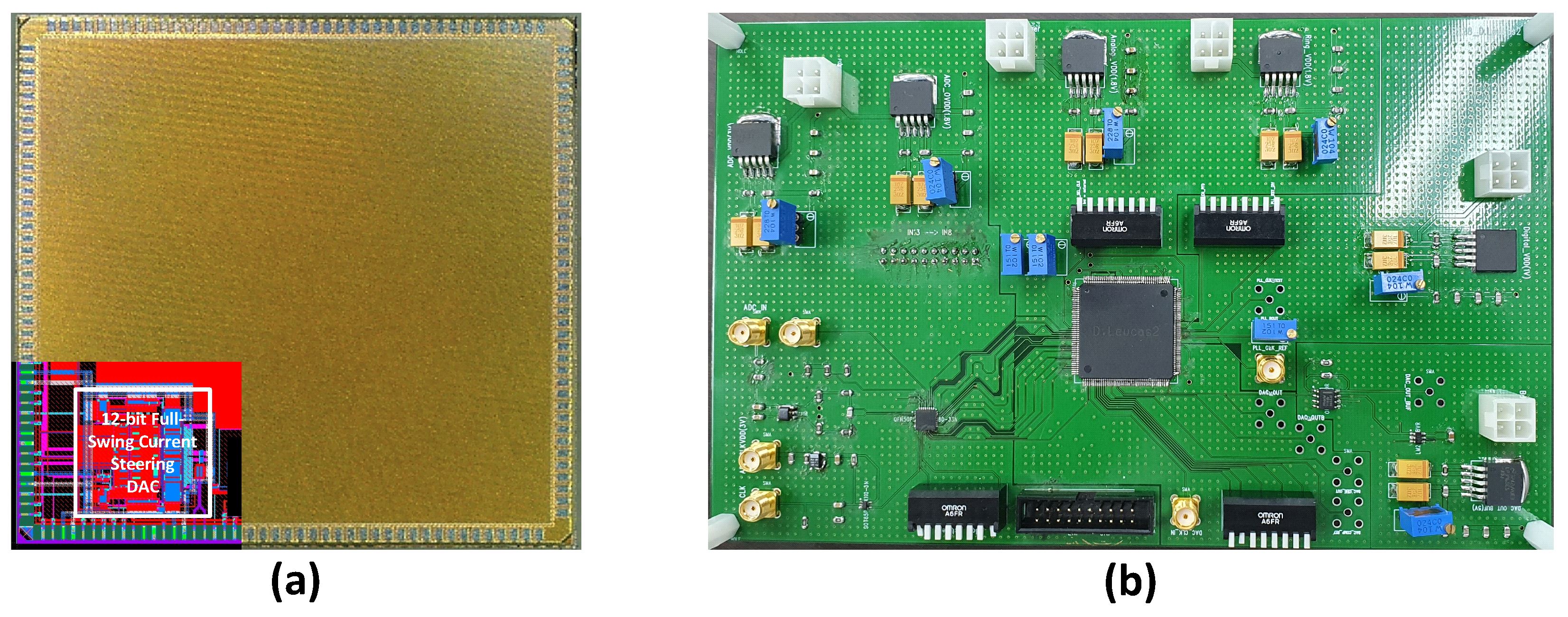
Figure 9a shows a photograph of the proposed DAC, which occupies an area of 0.95 mm × 0.93 mm on the full chip. Figure 9b shows a printed circuit board (PCB) used to test the DAC, and Figure 10 presents a block diagram of the measurement environment used for the evaluation. To generate the DAC input, we used a 14-bit ADC (LTC2254) and measured the DAC output with an oscilloscope.

Static/Dynamic Performance

Figure 11 shows the simulation results obtained when applying a ramping input signal to the proposed DAC. Figure 11 presents an enlarged view of the VDD/2 region with two cases: the voltage mismatch without half-power supply calibration and with half-power supply calibration. The proposed DAC employs thick-gate devices and operates with a 1.8 V analog supply voltage, achieving a resolution of 12 bits. Therefore, the 1LSB voltage of the proposed DAC is 0.44 mV. Figure 11 shows that when the half-power supply calibration technique was not applied, the voltage mismatch at VDD/2 was approximately 5.457 mV, resulting in a DNL of about 11.4 LSB. When the half-power supply calibration technique was applied, the voltage mismatch at VDD/2 was approximately 0.381 mV, resulting in a DNL of about 0.86 LSB. Therefore, when the half-power supply calibration technique is applied, the voltage mismatch at VDD/2 can be reduced by more than 92.5%.
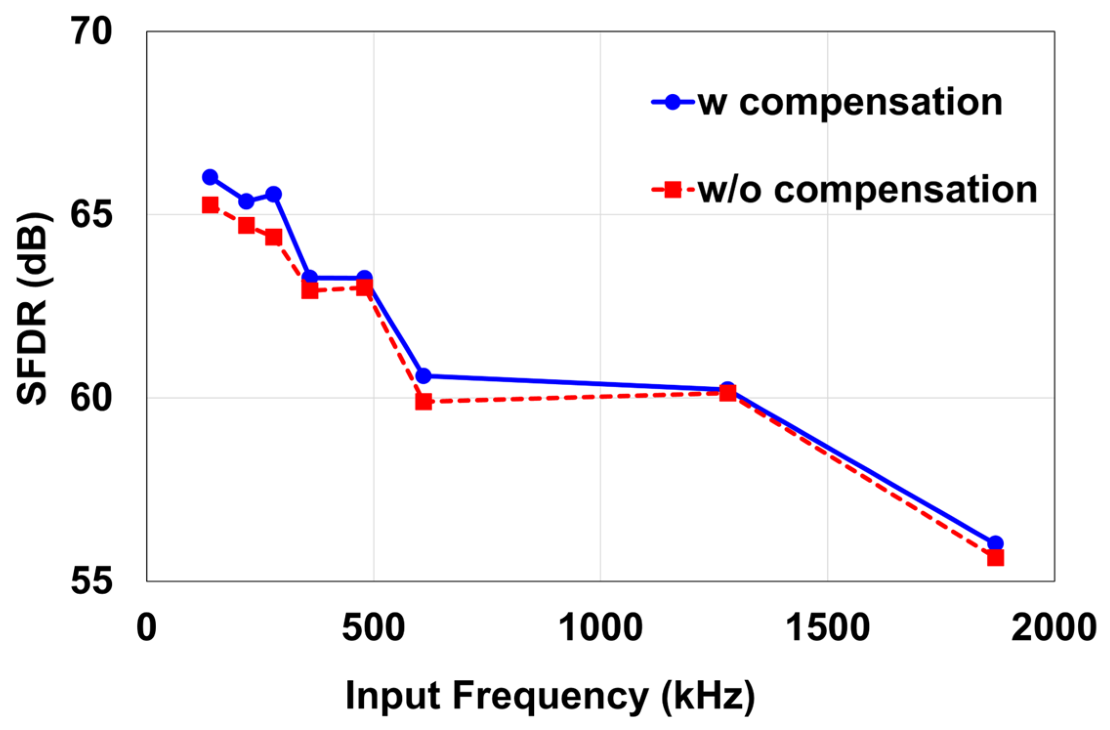
Figure 12 shows the SFDR measurement results. When no compensation operation was performed, the SFDR was approximately 65.26 dB. And when the compensation operation was performed, the SFDR was approximately 66.02 dB. Therefore, it was confirmed that the compensation operation improved the SFDR, ranging from 0.09 dB to 1.16 dB. These measurements confirmed that the proposed DAC’s SFDR performance could be improved through compensation operations. However, the ENOB at 100 MSPS was found to be approximately 10 bits. This is caused by mismatches due to comparator offsets, etc., and it appears that improvements could be made using dynamic element matching or the data weighted averaging method [17,18,19].
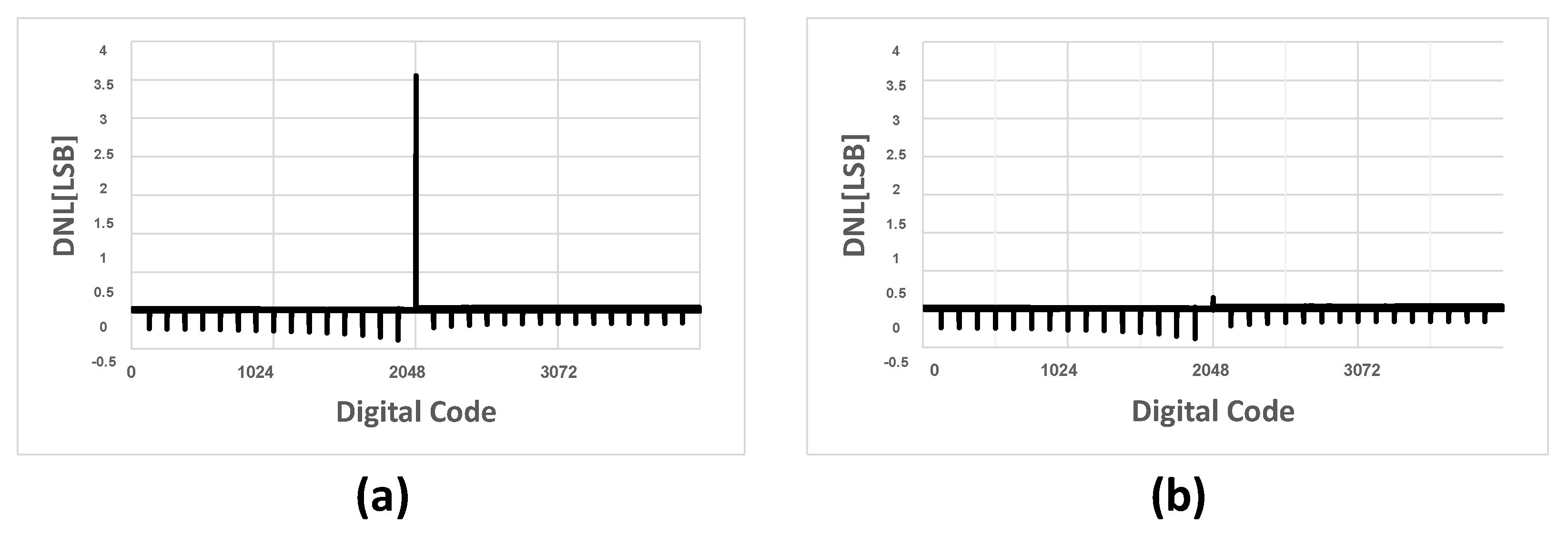
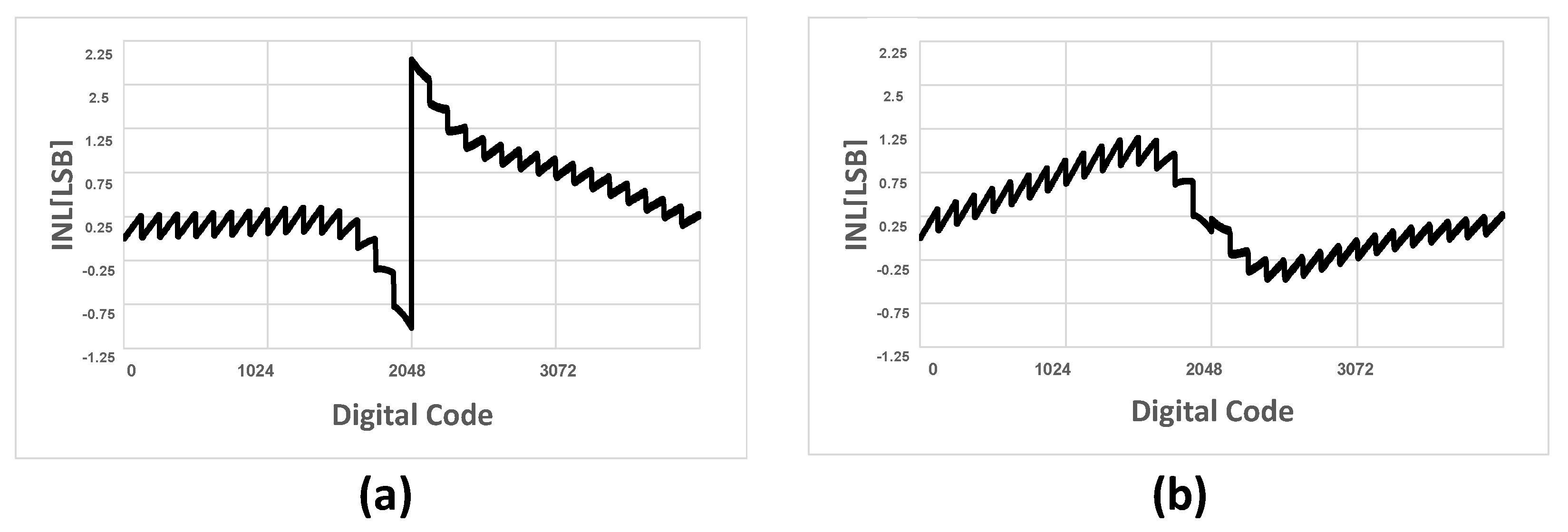
Figure 13 shows the DNL measurement results for the proposed DAC, where Figure 13a,b present the results without and with half-power supply calibration, respectively. Figure 13a shows that the DNL without half-power supply calibration was approximately 3.06 LSB, while that with half-power supply calibration was approximately 0.39 LSB. Therefore, the DNL improved by approximately 2.67 LSB when using half-power supply calibration. Figure 14 shows the INL measurement results for the proposed DAC, where Figure 14a,b present the results without and with half-power supply calibration, respectively. The INL without half-power supply calibration was approximately 2.04 LSB, while that with half-power supply calibration was approximately 1.15 LSB. Therefore, the INL improved by approximately 0.89 LSB when using half-power supply calibration. Figure 13 shows the measured DNL and INL characteristics of the proposed DAC after applying the half-supply calibration. With the calibration enabled, the dominant mismatch at the VDD/2 transition is corrected, and the resulting DNL/INL curves appear considerably smoother compared with the uncalibrated case. The cascode implementation of the current cells also leads to some transistors operating in the linear region over part of the output swing, which lowers the effective output resistance and reduces the visible effect of device mismatch. Consequently, the measured linearity appears more uniform than expected from simulation alone. In addition, the DNL plot exhibits periodic components beyond the mid-code error. These arise from segmentation boundary effects, as the transitions between unary- and binary-coded segments generate repeating switching patterns. Such periodic tones are intrinsic to segmented DAC architectures and, although mitigated by the proposed calibration, they cannot be entirely eliminated.
Table 2 shows the performance of the proposed DAC in comparison with that of other state-of-the-art technologies introduced in [6,15,16,20,21]. Notably, the techniques in [6,15] provide full-swing DAC output. The Walden figure of merit (FoM) was used to compare each technique and the proposed DAC (Walden FoM = power consumption/[sampling rate × 2resolution]).

4. Conclusions

The DAC proposed in this paper provides a full-range output, and its linearity performance was enhanced by maximizing the 1 LSB voltage at low supply voltages. In addition, the DNL performance at VDD/2 was improved by more than 50% through the implementation of a half-power supply calibration circuit to correct the voltage mismatch at the half-VDD point observed in conventional full-swing DACs. Using the full-swing DAC proposed in this paper, rail-to-rail operation of analog circuits that receive the DAC’s output is possible; as such, it is expected to be useful in devices such as display drivers and medical equipment. Furthermore, as process technology advances, power supply voltages are decreasing; however, the threshold voltage of analog MOSFETs do not decrease proportionally, resulting in a decrease in the usable output voltage range. Therefore, the 1LSB voltage of the data converter decreases and a resulting decrease in linearity becomes inevitable. However, when operating in the full-swing range, the 1LSB voltage can be effectively increased, and thus, the linearity performance can be expected to be improved even when the power supply voltage is reduced.

Author Contributions

K.P., S.G.C. and M.S. conceived and designed the circuits. J.K., M.K., H.S. and S.Y.K. performed the experiments and analyzed the data. All authors have read and agreed to the published version of the manuscript.

Funding

This work was partly supported by the Institute of Information and Communications Technology Planning and Evaluation (IITP)–ITRC (Information Technology Research Center) grant, funded by the Korean government (MSIT) (IITP-2025-RS-2024-00438007, 50%) and the Technology Innovation Program (public–private joint investment semiconductor R&D program (K-CHIPS) to foster high-quality human resources) (RS-2023-00235137), funded by the Ministry of Trade, Industry and Energy (MOTIE, Korea) (1415187379, 50%).

Data Availability Statement

The datasets generated as part of the current study are available from the corresponding author upon reasonable request.

Acknowledgments

The chip fabrication and EDA tools were supported by the IC Design Education Center (IDEC), Republic of Korea.

Conflicts of Interest

The authors declare no conflicts of interest.

References

  1. Li, X.; Liu, Y.; Zhang, Q.; Wu, N.; Lee, H. A 14-Bit 500 MS/s CMOS DAC Using Complementary Switched Current Sources and Time-Relaxed Interleaving DRRZ. IEEE Trans. Circuits Syst. I Regul. Pap. 2014, 61, 2337–2347. [Google Scholar] [CrossRef]
  2. Park, C.U.; Chung, J.H.; Ryu, S.T. A 12-bit 1 GS/s Current-Steering DAC with Paired Current Source Switching Background Mismatch Calibration. In Proceedings of the 2023 IEEE Custom Integrated Circuits Conference (CICC), San Antonio, TX, USA, 23–26 April 2023; IEEE: Piscataway, NJ, USA, 2023. [Google Scholar] [CrossRef]
  3. Sun, Y.; Zhang, Z.; Shan, Y.; Lang, L.; Dong, Y. Modeling and Mitigating Output-Dependent Modulation in Current-Steering DAC Based on Differential-Quad Switching Scheme. Electronics 2024, 13, 1992. [Google Scholar] [CrossRef]
  4. Duan, B.; Bi, J.; Xu, H.; Li, G.; Tian, Y.; Yan, N. A 12-bit 2 GS/s Current-Steering DAC with 27 mW Power Consumption in 28 nm CMOS. Microelectron. J. 2025, 163, 106756. [Google Scholar] [CrossRef]
  5. Zhuang, Y.; Zhang, L.; Zhang, Y.; Zhang, H. High-Purity Sine Wave Generation Using Nonlinear DAC with Predistortion Based on Low-Cost Accurate DAC–ADC Co-Testing. IEEE Trans. Instrum. Meas. 2018, 67, 279–287. [Google Scholar] [CrossRef]
  6. Park, G.; Song, M. A CMOS Current-Steering D/A Converter with Full-Swing Output Voltage and a Quaternary Driver. IEEE Trans. Circuits Syst. II Express Briefs 2015, 62, 671–675. [Google Scholar] [CrossRef]
  7. Kim, J.M.; Jung, W.Y. A Fully Integrated Circuit for High Current Multiple-Output. IDEC J. Integr. Circuits Syst. 2023, 9, 11–15. [Google Scholar] [CrossRef]
  8. Song, D.; Cho, G.; Kim, J. A 2.5 GHz, 87-fs Step, Temperature-and-Voltage-Tolerant 6-bit Digital-to-Time Converter in 28 nm CMOS. IDEC J. Integr. Circuits Syst. 2025, 11, 14–19. [Google Scholar] [CrossRef]
  9. Razavi, B. The Current-Steering DAC [A Circuit for All Seasons]. IEEE Solid-State Circuits Mag. 2018, 10, 11–15. [Google Scholar] [CrossRef]
  10. Li, X.; Zhou, L. A Survey of High-Speed High-Resolution Current Steering DACs. J. Semicond. 2020, 41, 111402. [Google Scholar] [CrossRef]
  11. Wang, F.; Wang, Z.; Liu, J.; Yu, F. A 14-Bit 3-GS/s DAC Achieving SFDR > 63 dB Up to 1.4 GHz With Random Differential-Quad Switching Technique. IEEE Trans. Circuits Syst. II Express Briefs 2022, 69, 879–883. [Google Scholar] [CrossRef]
  12. Ravinuthula, V.R.; Sahoo, B.; Halder, S.; Seshan, M.; Cao, C. A 14-Bit 8.9 GS/s RF DAC in 40 nm CMOS Achieving >71 dBc LTE ACPR at 2.9 GHz. In Proceedings of the 2016 IEEE Symposium on VLSI Circuits, Honolulu, HI, USA, 15–17 June 2016; IEEE: Piscataway, NJ, USA, 2016; pp. 1–2. [Google Scholar] [CrossRef]
  13. Luo, F.J.; Li, X.Y.; Tang, X.F.; Wang, H.Y.; Xu, X.W. Current Switch Driver and Current Source Designs for High-Speed Current-Steering DAC. In Proceedings of the 2008 2nd International Conference on Anti-Counterfeiting, Security and Identification, Guiyang, China, 20–23 August 2008; IEEE: Piscataway, NJ, USA, 2008; pp. 364–367. [Google Scholar] [CrossRef]
  14. Tong, X.; Liu, D. High SFDR Current-Steering DAC With Splitting-and-Binary Segmented Architecture and Dynamic-Element-Matching Technique. IEEE Trans. Circuits Syst. II Express Briefs 2022, 69, 4233–4237. [Google Scholar] [CrossRef]
  15. Mehrjoo, M.S.; Buckwalter, J.F. A 10-Bit, 300 MS/s Nyquist Current-Steering Power DAC with 6 V Output Swing. IEEE J. Solid-State Circuits 2014, 49, 1408–1418. [Google Scholar] [CrossRef]
  16. Huang, C.Y.; Chen, Y.H.; Lin, T.Y.; Liu, S.I. Design of 12-Bit 100-MHz Current-Steering DAC for SoC Applications. In Proceedings of the Fifth International Workshop on System-on-Chip for Real-Time Applications (IWSOC’05), Banff, AB, Canada, 20–24 July 2005; IEEE: Piscataway, NJ, USA, 2005; pp. 117–122. [Google Scholar] [CrossRef]
  17. Wang, D.; Liu, J.; Jin, X.; Ren, J.; Zhang, X.; He, Z. A 3 GS/s 12-Bit Current-Steering Digital-to-Analog Converter with Partial Randomization Dynamic Element Matching (PRDEM). Electronics 2019, 8, 464. [Google Scholar] [CrossRef]
  18. Remple, J.; Panigada, A.; Galton, I. An ISI Scrambling Technique for Dynamic Element Matching Current-Steering DACs. IEEE J. Solid-State Circuits 2021, 56, 2702–2713. [Google Scholar] [CrossRef]
  19. Lin, W.-T.; Huang, H.-Y.; Kuo, T. A 12-bit 40-nm DAC Achieving SFDR > 70 dB at 1.6 GS/s with DEMDRZ Technique. IEEE J. Solid-State Circuits 2020, 55, 3300–3312. [Google Scholar] [CrossRef]
  20. Bonsu, G.; Tamakloe, K.; Bruce, I.; Nti Darko, E.; Chen, D. Redundancy-Interpolated Three-Segment DAC with On-Chip Digital Calibration for Improved Static Linearity. Electronics 2025, 14, 3477. [Google Scholar] [CrossRef]
  21. Deng, Y.; Yang, P.; Huang, G.; Liu, J.; Ren, Z.; Fan, Y.; Song, Z. A 14-Bit Digital to Analog Converter for a Topmetal-CEE Pixel Readout Chip. Electronics 2024, 13, 3074. [Google Scholar] [CrossRef]
Figure 1. The proposed DAC architecture.
Electronics 14 03955 g001
Figure 2. (a) Block diagram of the symmetric thermometer decoder and (b) an example of the operation of 4- to 7-bit decoding.
Electronics 14 03955 g002
Figure 3. Equivalent circuit of a current cell according to its output impedance.
Electronics 14 03955 g003
Figure 4. Circuit diagram of the current cells.
Electronics 14 03955 g004
Figure 5. Operating regions of current cells.
Electronics 14 03955 g005
Figure 6. (a) Circuit diagram and (b) simulation result of quaternary driver.
Electronics 14 03955 g006
Figure 7. (a) Output waveform of each current cell and (b) circuit structure of the output selector.
Electronics 14 03955 g007
Figure 8. Block diagram of the proposed half-power supply calibration circuit.
Electronics 14 03955 g008
Figure 9. (a) Chip photograph; (b) PCB used to measure the proposed DAC.
Electronics 14 03955 g009
Figure 10. Block diagram of the measurement environment for evaluation of the proposed DAC.
Electronics 14 03955 g010
Figure 11. Ramp input simulation of the proposed DAC with voltage mismatch at VDD/2: (a) without half-power supply calibration and (b) with half-power supply calibration.
Electronics 14 03955 g011
Figure 12. SFDR measurement results when the proposed DAC with compensation operation (blue, solid line) and without compensation (red, dashed line) at 100 MSPS when the input signal frequency is swept from 140 kHz to 1870 kHz).
Electronics 14 03955 g012
Figure 13. DNL measurement results: (a) without half-power supply calibration and (b) with half-power supply calibration.
Electronics 14 03955 g013
Figure 14. INL measurement results: (a) without calibration and (b) with calibration.
Electronics 14 03955 g014
Table 1. W/Ls of unit current cells and σ/μ of current.
SegmentsnMOS CellspMOS Cells
W/L (μm/μm)σ/μ of Current (%)W/L (μm/μm)σ/μ of Current (%)
LLSB1/1.040.451/1.040.47
LSB5/1.040.2310/1.040.19
MSB40/0.260.1273.5/0.260.09
Table 2. Performance comparison.
This Work[6][15][16][20][21]
Full-swingYesYesYesNoNoNo
Resolution12-b6-b10-b12-b16-b14-b
Technology28 nm CMOS0.11 μm CMOS40 nm CMOS0.35 μm CMOS0.18 μm CMOS0.18 μm CMOS
Sampling rate100 MS/s1 GS/s300 MS/s100 MS/s500 MS/s500 MS/s
INL/DNL0.39 LSB
1.15 LSB
0.7 LSB
0.7 LSB
0.6 LSB
0.4 LSB
0.4 LSB
0.25 LSB
0.48 LSB
0.68 LSB
1.57 LSB
1.07 LSB
Power
consumption
79.65 mW19.1 mW476 mW47 mW630 mW0.3 mW
Core area0.89 mm20.46 mm22.25 mm26.9 mm2-0.02 mm2
FoM (Walden)194.46 fJ298.4 fJ1550 fJ114.7 fJ0.21 fJ13 fJ
Disclaimer/Publisher’s Note: The statements, opinions and data contained in all publications are solely those of the individual author(s) and contributor(s) and not of MDPI and/or the editor(s). MDPI and/or the editor(s) disclaim responsibility for any injury to people or property resulting from any ideas, methods, instructions or products referred to in the content.