1. Introduction
Lighting plays a fundamental role in human life, far exceeding basic visual needs. It influences physical health, enhances environmental aesthetics, supports economic productivity, and ensures safety in various environments. Therefore, the development and optimization of lighting sources remain a key area for further research and technological advancement. Lighting sources are indispensable in modern life, encompassing functional, psychological, economic, and environmental dimensions. Strategic design and implementation of lighting systems not only improve quality of life but also enhance safety, efficiency, and sustainability across various industries. As lighting technology continues to evolve, its social significance will grow increasingly important, underscoring the necessity for interdisciplinary research and innovation in this field. The benefits and impacts of lighting sources in our daily lives are as follows: (1) Human vision and visual comfort: The most immediate and essential function of lighting is to facilitate human vision. Adequate illumination allows for accurate visual perception, which is indispensable for daily activities, occupational tasks, and recreational engagement. Proper lighting reduces visual fatigue, enhances contrast sensitivity, and improves performance in both residential and professional environments. Inadequate or poorly designed lighting can lead to eye strain, decreased productivity, and increased incidence of errors and accidents. (2) Psychological and physiological impacts: Scientific studies have established that lighting conditions significantly affect human circadian rhythms, mood, and cognitive functioning. Exposure to appropriate lighting at specific times of day helps regulate melatonin production and promotes healthy sleep–wake cycles. Natural daylight and high-quality artificial lighting can improve alertness, reduce symptoms of depression, and enhance overall psychological well-being. Therefore, lighting design has become a crucial component in architectural and healthcare applications. (3) Safety and security: Lighting is a key factor in ensuring personal and public safety. In urban infrastructure, streetlights and traffic signals enhance visibility for pedestrians and drivers, thereby reducing the risk of accidents. In industrial and commercial settings, well-illuminated environments prevent workplace injuries and enable the safe operation of machinery. Emergency lighting systems are vital for facilitating evacuation during power outages or hazardous events. (4) Economic and industrial significance: Illumination directly influences economic activity by enabling extended operational hours and improving working conditions. In sectors such as manufacturing, retail, healthcare, and education, appropriate lighting increases efficiency and supports task-specific requirements. Moreover, the lighting industry itself constitutes a significant segment of the global economy, with substantial investments in research, innovation, and sustainable development. (5) Aesthetic and cultural value: Lighting contributes to the aesthetic quality of built environments, shaping perceptions of space, color, and texture. It is an essential element in interior and architectural design, as well as in cultural and artistic expression, such as theater, photography, and public installations. The ability to manipulate light color, intensity, and direction provides designers with a versatile tool for enhancing user experience and ambiance. (6) Environmental considerations: With growing concerns about energy consumption and environmental sustainability, lighting technologies have come under increased scrutiny. Traditional lighting sources often involve significant energy losses and the use of hazardous materials. The shift toward energy-efficient lighting, particularly light-emitting diodes (LEDs), has contributed to reductions in greenhouse gas emissions and resource consumption. Thus, lighting also plays a pivotal role in global sustainability efforts [
1,
2].
In recent years, the development of solid-state lighting technologies, particularly light-emitting diode (LED) lamps, has significantly transformed the lighting industry. A comprehensive comparison between traditional lighting sources and LED lighting, with a focus on their respective advantages and disadvantages in terms of energy efficiency, operational characteristics, environmental impact, and economic considerations, is addressed as follows. (1) Energy efficiency: Traditional lighting sources exhibit relatively low luminous efficacy, typically offering approximately 60–100 lm/W efficiency; however, they still fall short when compared to LED technology. In contrast, LED lamps demonstrate superior energy efficiency, often exceeding 100 lm/W and reaching up to 150 lm/W in high-performance applications. This improvement results in significant reductions in electricity consumption and operational costs over time. (2) Lifespan and maintenance: The operational lifespan of traditional lighting sources is limited and may achieve 6000 to 15,000 h of use. LEDs, on the other hand, offer an extended service life, commonly rated at 25,000 to 50,000 h or more. Consequently, the maintenance frequency and associated costs for LED systems are substantially reduced, particularly in large-scale or hard-to-access installations. (3) Thermal characteristics: One of the major drawbacks of traditional lighting is excessive heat generation. Traditional lighting sources convert a significant portion of electrical energy into thermal energy, which not only reduces efficiency but also increases the risk of thermal damage or fire. LED lamps operate at much lower temperatures, making them inherently safer and more energy-efficient. (4) Durability and reliability: Traditional lighting technologies often rely on fragile components such as filaments or glass tubes, which are susceptible to mechanical shock and vibration. LEDs, being solid-state devices, are inherently more robust and resistant to external impacts. This attribute enhances their reliability and makes them suitable for a wide range of indoor and outdoor applications. (5) Environmental and health considerations: Traditional lighting sources, such as fluorescent lamps, contain small amounts of mercury, a hazardous substance that poses environmental and health risks if improperly disposed of. Additionally, the higher energy consumption of traditional lighting contributes to increased greenhouse gas emissions. LEDs are free of toxic materials and, due to their high efficiency, help minimize environmental impact by reducing both energy use and carbon footprint. (6) Light quality and control: In contrast to traditional lighting sources, LEDs provide a wide range of correlated color temperatures (CCTs) and can achieve high color rendering index (CRI) values (>80, and up to 95 for premium products). Moreover, LED systems are compatible with advanced control features, including dimming, color tuning, and smart connectivity, although some models may require compatible dimmer circuits. (7) Economic considerations: While traditional lighting sources generally have a lower initial cost, their short lifespan and high energy consumption result in higher long-term operational expenses. LED lamps involve a higher upfront investment; however, the total cost of ownership is often lower due to savings in energy and maintenance. In summary, while traditional lighting sources offer certain benefits—such as high color fidelity and low initial costs—they are generally surpassed by LED lamps in terms of energy efficiency, longevity, safety, and environmental sustainability. The transition to LED lighting represents a significant advancement in modern illumination technology and supports global initiatives for energy conservation and sustainable development [
3,
4,
5,
6,
7,
8,
9,
10,
11,
12,
13,
14,
15,
16,
17,
18,
19].
In power electronic systems, snubber circuits are essential for protecting switching devices from voltage spikes and reducing switching losses caused by parasitic inductances. Traditional snubber configurations, such as resistor–capacitor (RC) or resistor–capacitor–diode (RCD) networks, dissipate excess energy as heat, resulting in power loss and reduced efficiency. In contrast, lossless snubber circuits are designed to recover and recycle this energy, thereby enhancing overall system efficiency. A lossless snubber circuit redirects the energy stored in the parasitic elements during switching transitions back to the power source or to a storage component, such as a capacitor or inductor, without significant energy dissipation. These circuits are typically composed of passive components (inductors, capacitors, and diodes) and occasionally include active switches to control the energy recovery process. Advantages and features of the lossless snubber circuit are addressed as follows. (1) High efficiency: Lossless snubbers minimize power dissipation by recovering the switching energy, making them highly suitable for high-efficiency power converters. (2) Improved thermal management: By avoiding resistive dissipation, less heat is generated, which reduces thermal stress on components and simplifies the thermal design. (3) Reduced electromagnetic interference (EMI): Properly designed lossless snubber circuits can smooth voltage and current transitions, thereby reducing high-frequency EMI emissions. (4) Extended switch lifespan: By limiting voltage spikes and reducing turn-off losses, the electrical stress on switching devices is minimized, enhancing their reliability and lifespan. (5) Energy recycling capability: The inherent energy recovery mechanism contributes to power conservation, especially in systems where switching frequency and load dynamics vary significantly. (6) Scalability and adaptability: Lossless snubber designs can be adapted to various converter topologies, including flyback, forward, and resonant converters, offering flexible integration into modern power systems [
20,
21,
22,
23,
24,
25,
26,
27,
28,
29].
To address the need for efficient power conversion and improved input current quality, this paper proposes and implements a novel LED electronic lighting driver circuit featuring input current shaping capability. The proposed topology integrates a lossless snubber circuit with a flyback converter to realize an isolated, single-switch power conversion architecture, herein referred to as a modified flyback converter. Furthermore, the transformer’s magnetizing inductor within the proposed driver is designed to operate in discontinuous conduction mode (DCM), thereby inherently achieving power factor correction (PFC) without the need for additional circuitry. The original concept of the proposed circuit is described in [
30], and this paper is an expanded version of [
30] with improvements in content for applications with higher LED output power. The remainder of this paper is structured as follows.
Section 2 provides a detailed description and analysis of the operational modes of the proposed isolated AC-DC LED electronic lighting driver circuit incorporating power factor correction.
Section 3 discusses the key design considerations associated with the proposed driver architecture. In
Section 4, experimental results obtained from a fabricated prototype are presented to validate the circuit’s performance. Finally,
Section 5 concludes the paper with a summary of the findings.
2. Descriptions and Analysis of the Isolated AC-DC LED Electronic Lighting Driver Circuit with Power Factor Correction
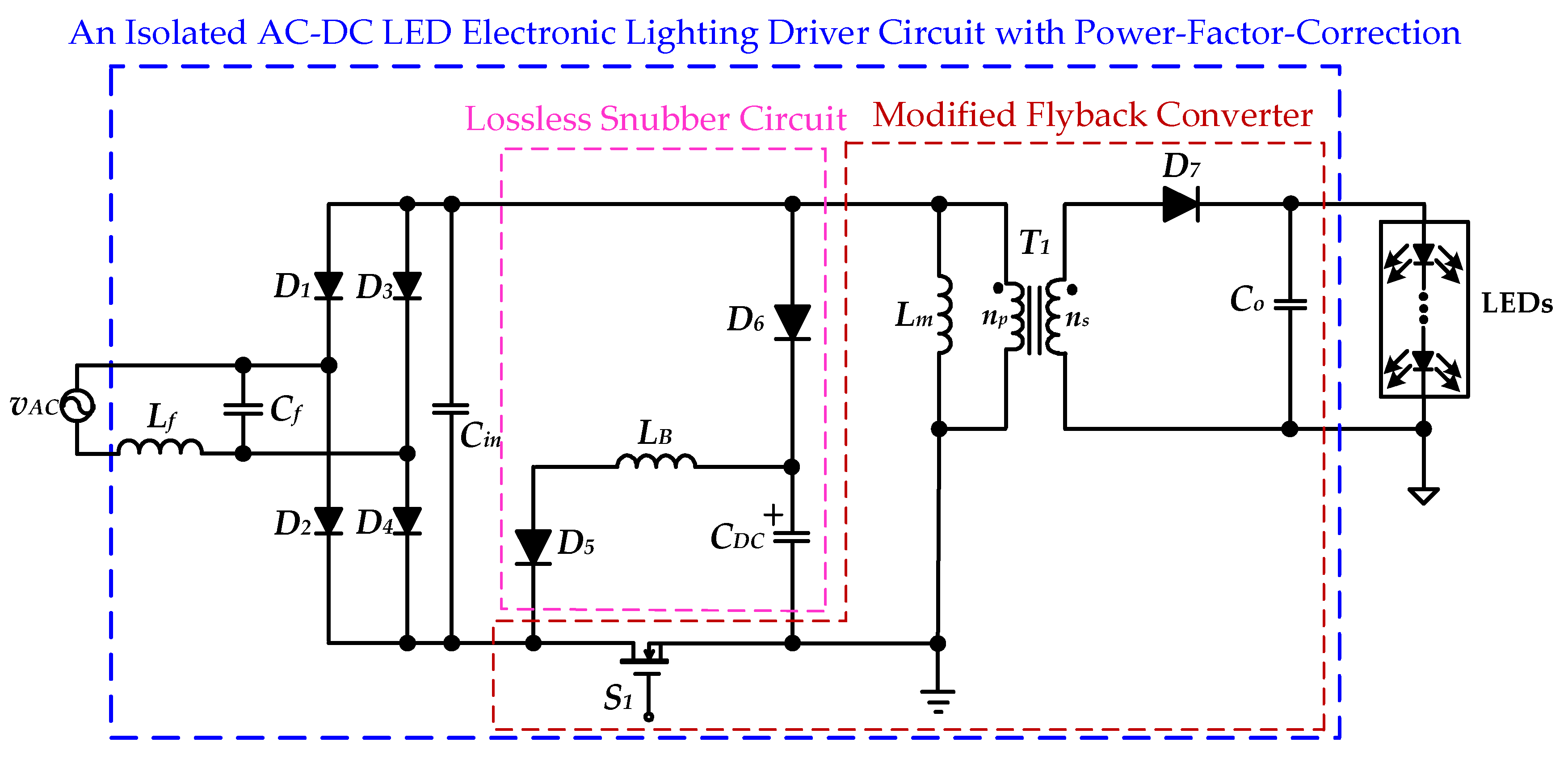
Figure 1 shows the proposed AC-DC LED electronic lighting driver circuit with power factor correction, which consists of a lossless snubber circuit and a modified flyback converter as the main circuit, and the entire isolated AC-DC LED electronic lighting driver circuit topology includes a filter inductor
Lf, a filter capacitor
Cf, a full-wave rectifier (including four diodes
D1,
D2,
D3, and
D4), a power switch
S1, an inductor
LB, three diodes
D5,
D6 and
D7, a DC-linked capacitor
CDC, a transformer
T1 with a turn
np in the primary-side and a turn
ns in the secondary-side, an output capacitor
Co and the LEDs.
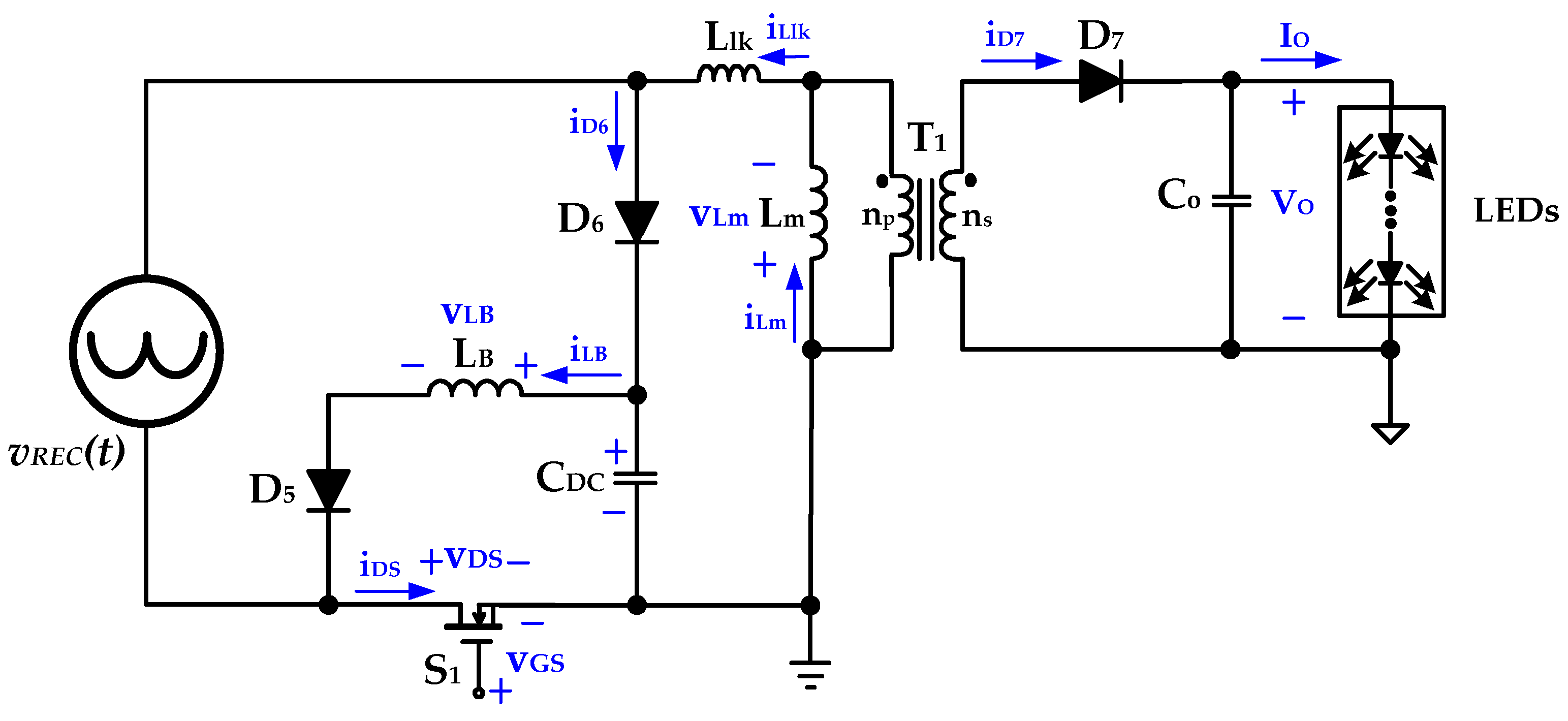
Figure 2 shows the equivalent circuit of the isolated AC-DC LED electronic lighting driver circuit with power factor correction, obtained while analyzing the operational modes. In order to analyze the circuit operation of the proposed isolated AC-DC LED electronic lighting driver circuit with power factor correction, the following assumptions were made.
- (a)
The input AC voltage source vAC is connected to the filter inductor Lf and filter capacitor Cf and rectified by a full-bridge rectifier, and then the voltage presented on the input capacitor Cin is denoted as vREC(t).
- (b)
The magnetizing inductor Lm of the transformer T1 is designed to operate in discontinuous conduction mode (DCM), and Llk is the leakage inductance of the transformer T1, respectively. In addition, the values of leakage inductors Llk are much smaller than the magnetizing inductor Lm; therefore, the voltage drops of the leakage inductor Llk can be neglected.
- (c)
The intrinsic diode and the turn-on resistor of the power switch S1 are neglected.
- (d)
Neglect the on-state voltage drops and equivalent resistance of diodes D5 and D6 and output diode D7.
- (e)
The rest of the circuit elements are considered ideal.
Figure 3,
Figure 4,
Figure 5,
Figure 6,
Figure 7 and
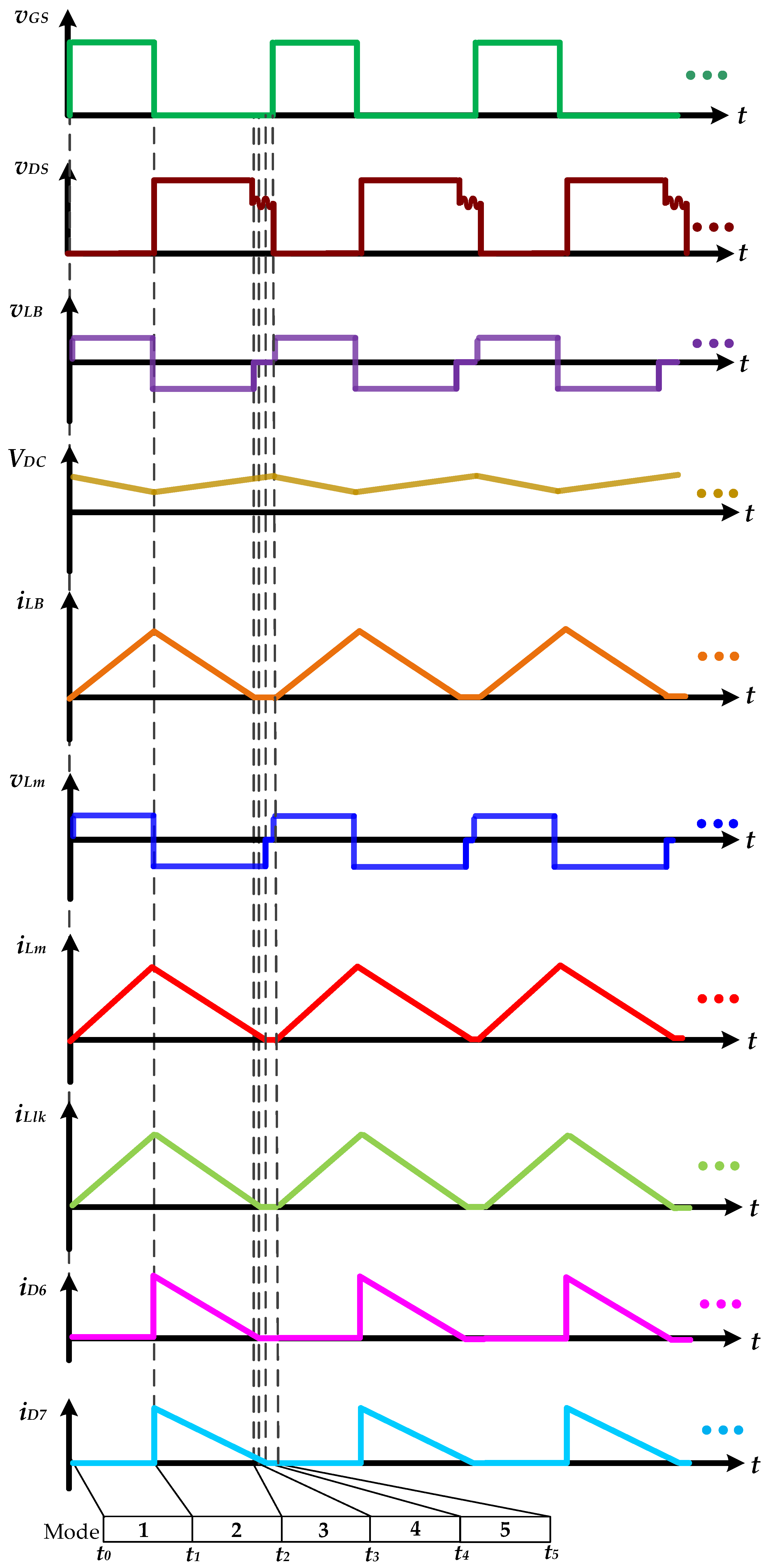
Figure 8 illustrate the operating modes and theoretic waveforms of the isolated AC-DC LED electronic lighting driver circuit with power factor correction, respectively, and each operation mode is analyzed and introduced in detail below.
Operation Mode 1 (
t0 ≤
t <
t1):
Figure 3 represents the operation mode 1 of the isolated AC-DC LED electronic lighting driver circuit with power factor correction. At time
t0, the power switch
S1 is driven on and starts to enter operation mode 1. The full-wave rectified voltage
vREC(t) is supplied to the magnetizing inductor
Lm and the leakage inductor
Llk via the power switch
S1; the magnetizing inductor current
iLm and the leakage inductor current
iLlk show a linear rise; the DC-linked capacitor
CDC is supplied to the inductor
LB via the power switch
S1 and the diode
D5; and the inductor current
iLB shows a linear rise, and the output capacitor
Co provides energy to the LEDs. At time
t1, the inductor currents
iLm and
iLB will reach their maximum values, and operation mode 1 ends when the power switch
S1 cuts off at time
t1.
Operational Mode 2 (
t1 ≤
t <
t2):
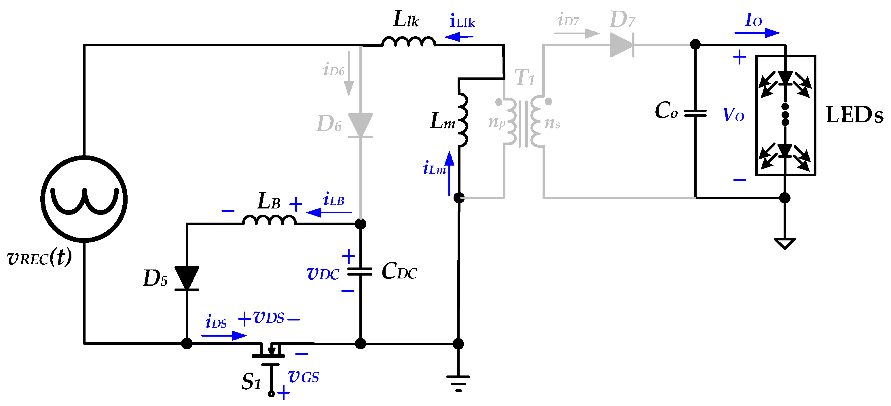
Figure 4 represents the operation mode 2 of the isolated AC-DC LED electronic lighting driver circuit with power factor correction. At time
t1, the power switch
S1 cuts off and the diodes
D5 and
D6 are biased in the forward direction. The inductor
LB sends energy back to the full-wave rectified voltage
vREC(t) via diodes
D5 and
D6, and the inductor current
iLB decreases linearly. The magnetizing inductor
Lm and the leakage inductor
Llk are supplied with energy via diode
D6 to the DC-linked capacitor
CDC, and the magnetizing inductor current
iLm and the leakage inductor current
iLlk decrease linearly. In addition, the output diode
D7 on the secondary side of the transformer is forward biased, so the magnetizing inductor
Lm provides energy to the LEDs through the diode
D7, and operation mode 2 ends when the inductor
LB finishes releasing energy at time
t2.
Operational Mode 3 (
t2 ≤
t <
t3):
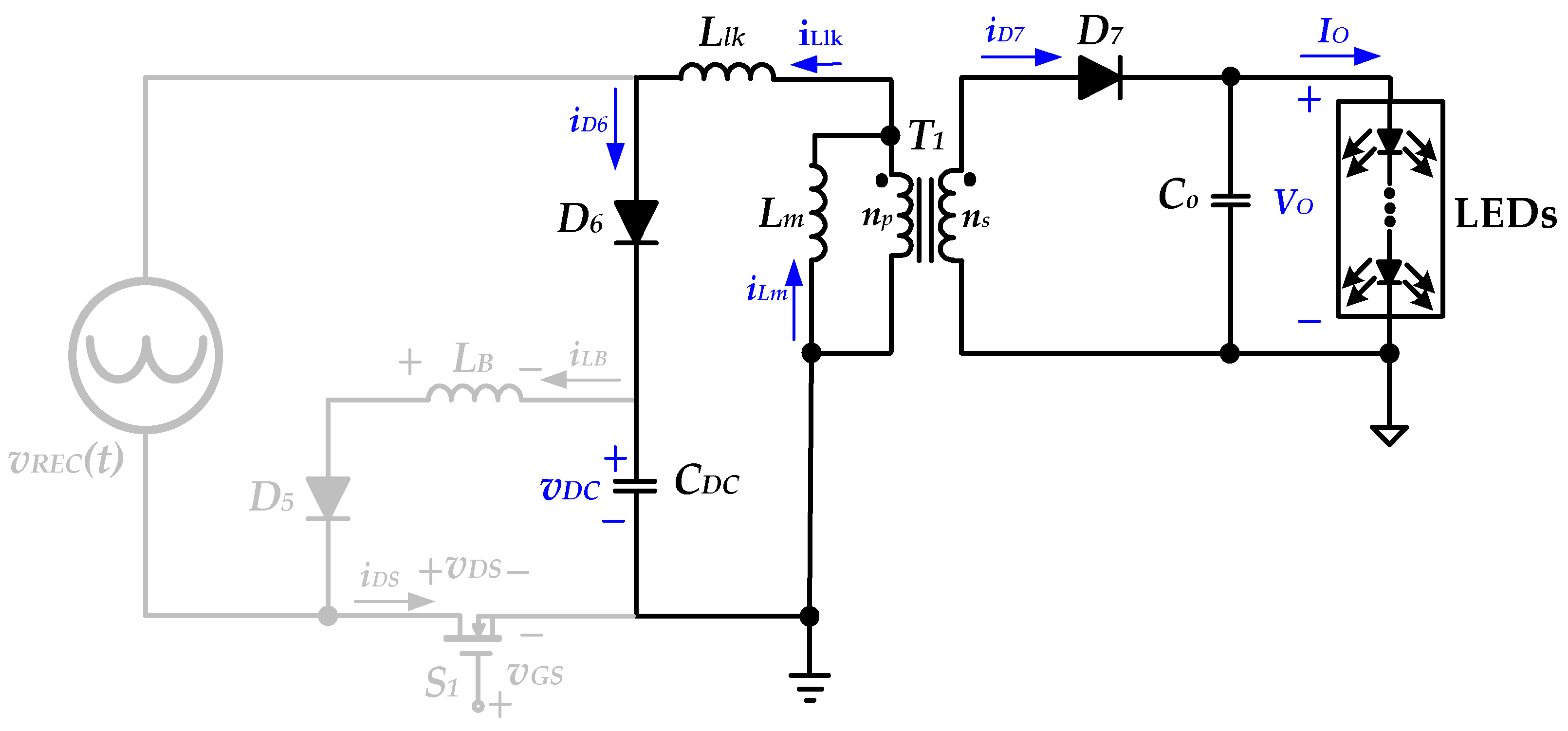
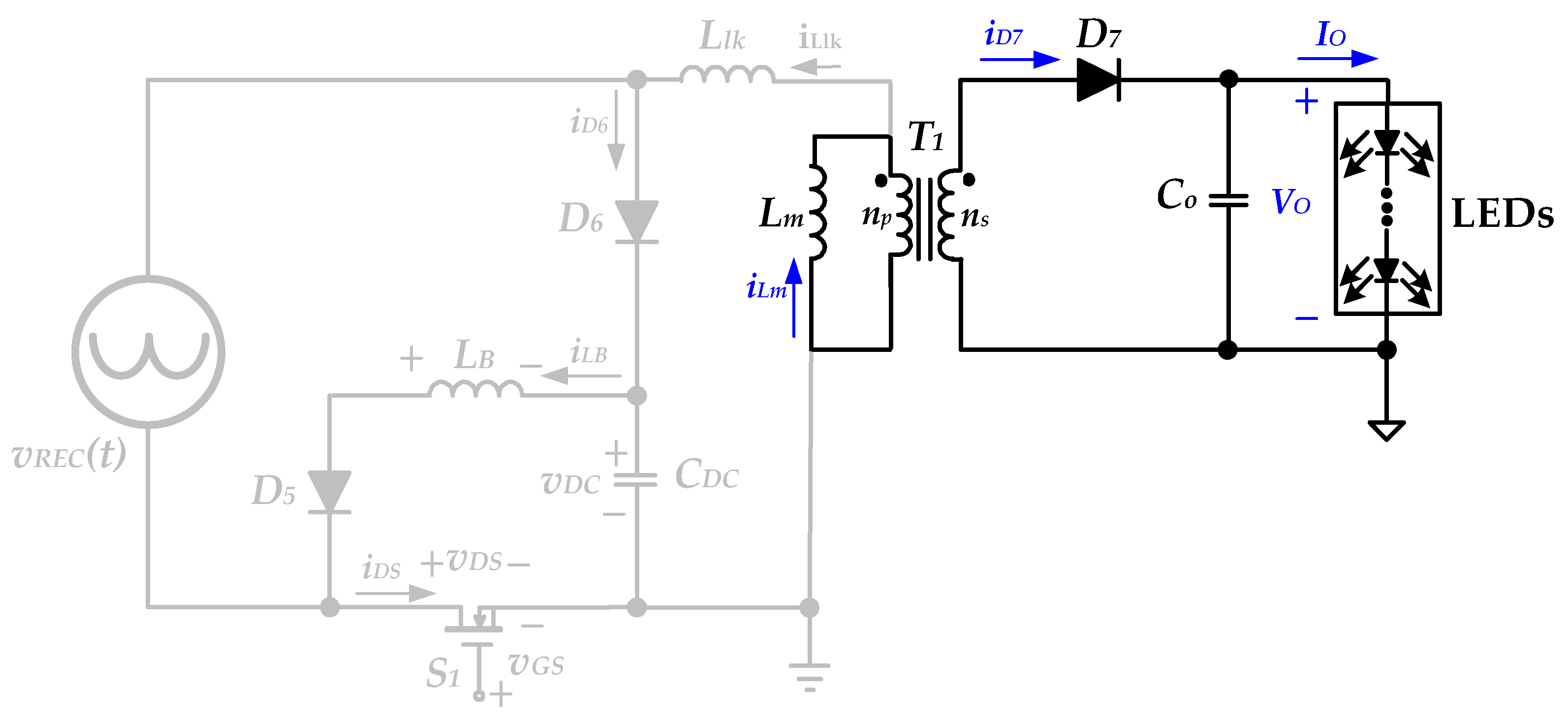
Figure 5 represents operation mode 3 of the isolated AC-DC LED electronic lighting driver circuit with power factor correction. In this mode, the magnetizing inductor
Lm and the leakage inductor
Llk continue to provide energy to the DC-linked capacitor
CDC via diode
D6 and continue to provide energy to the LEDs via diode
D7, and the magnetizing inductor current
iLm and the leakage inductor current
iLlk continue to decrease linearly. When the leakage inductor
Llk finishes releasing energy at time
t3, operation mode 3 ends.
Operational Mode 4 (
t3 ≤
t <
t4):
Figure 6 represents the operation mode 4 of the isolated AC-DC LED electronic lighting driver circuit with power factor correction. In this mode, the magnetizing inductor
Lm continues to provide energy to the LEDs via diode
D7, and the magnetizing inductor current
iLm continues to decrease linearly. When the magnetizing inductor
Lm finishes releasing energy at time
t4, operation mode 4 ends.
Operational Mode 5 (
t4 ≤
t <
t5):
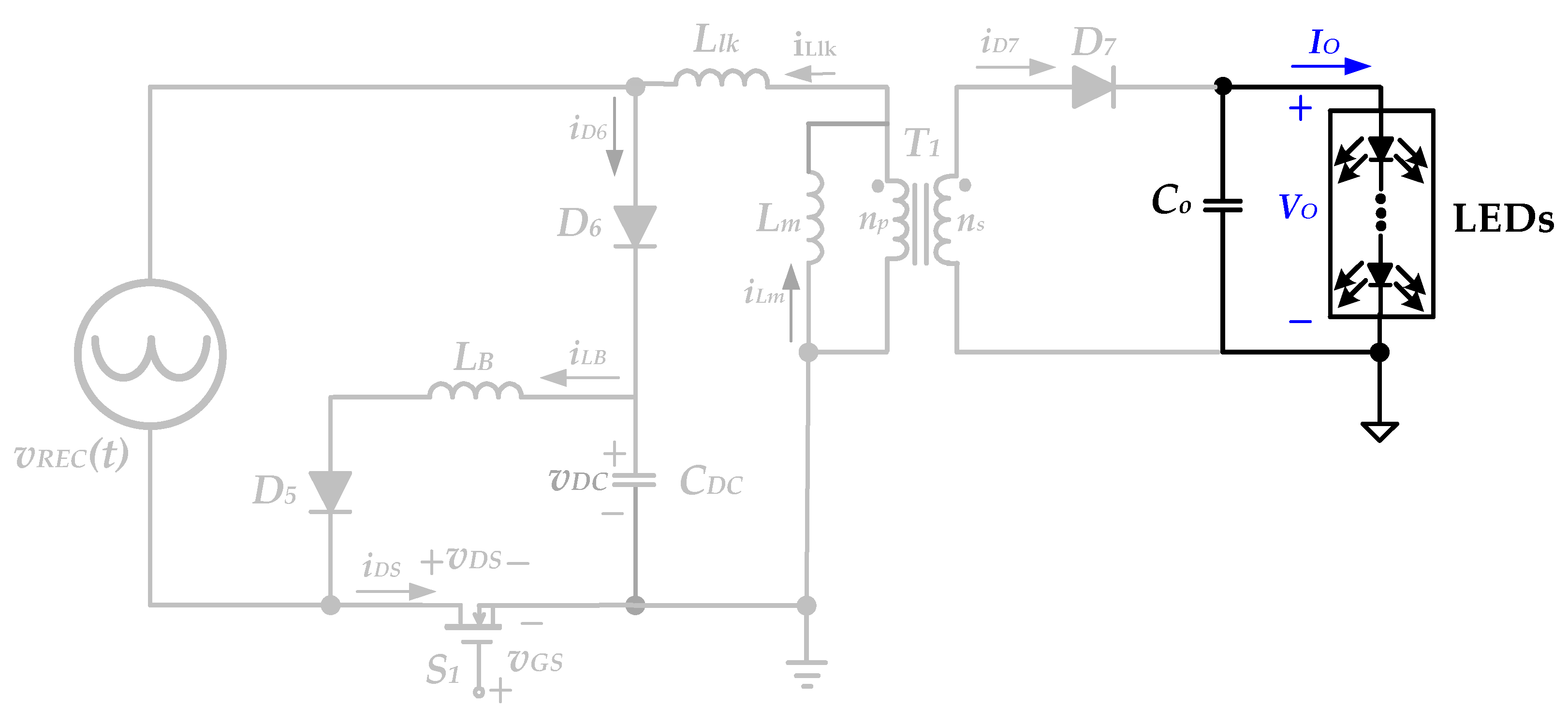
Figure 7 represents operation mode 5 of the isolated AC-DC LED electronic lighting driver circuit with power factor correction. In this mode, energy is supplied to the LEDs by the output capacitor
Co. When the power switch
S1 is turned on again at time
t5, operation mode 5 ends and the circuit reverts back to operation mode 1.
4. Experimental Results Obtained from the Implemented Prototype of the Isolated AC-DC LED Electronic Lighting Driver Circuit
A prototype isolated AC-DC LED electronic lighting driver circuit applied to an AC input voltage of 110 V root-mean-square (rms) value has been successfully implemented and tested for powering a 72 W-rated LEDs with an output rated voltage of 36 V and an output rated current of 2 A.
Table 1 and
Table 2 show the specifications and the key components used in the proposed isolated AC-DC LED electronic lighting driver circuit with power factor correction, respectively. Considering the variability of LED parameters in practical applications, a prototype of the proposed LED electronic lighting driver circuit was designed, implemented, and experimentally evaluated. The circuit employs a PWM control IC (TL494) to regulate both the voltage and current of the LED load, thereby ensuring operation at their respective nominal values.
Figure 10 illustrates the experimentally measured gate-driving signal
VGS of the power switch. The switching frequency and duty cycle were set to 40 kHz and 0.25, respectively.
Figure 11 presents the corresponding measured waveforms of the switch voltage
VDS and switch current
IDS. As illustrated in
Figure 11, a substantial voltage is observed across (
VDS) during the conduction period of the MOSFET. The MOSFET employed in the prototype driver circuit (STP20NM60), which is commonly available in our laboratory, exhibits a channel resistance (
RDSon) of 0.29 Ω. Consequently, considerable conduction losses occur in the device, leading to a reduction in overall circuit efficiency. To enhance conversion efficiency, future work may consider replacing the existing MOSFET with one possessing a lower (
RDSon), thereby mitigating conduction losses and improving the performance of the LED driver circuit.
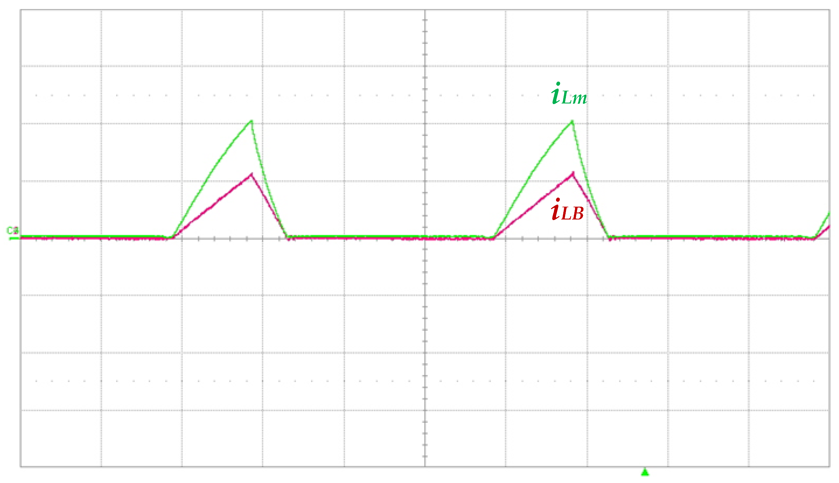
Figure 12 depicts the measured currents of the magnetizing inductor (
iLm) and the secondary inductor (
iLB), both operating in discontinuous conduction mode (DCM). In addition, both inductor currents exhibit an extended interval of discontinuity. This behavior arises because the experimental waveforms illustrated in
Figure 12 were obtained at an operating point significantly distant from the peak value of the input voltage (i.e., at 90 degrees).
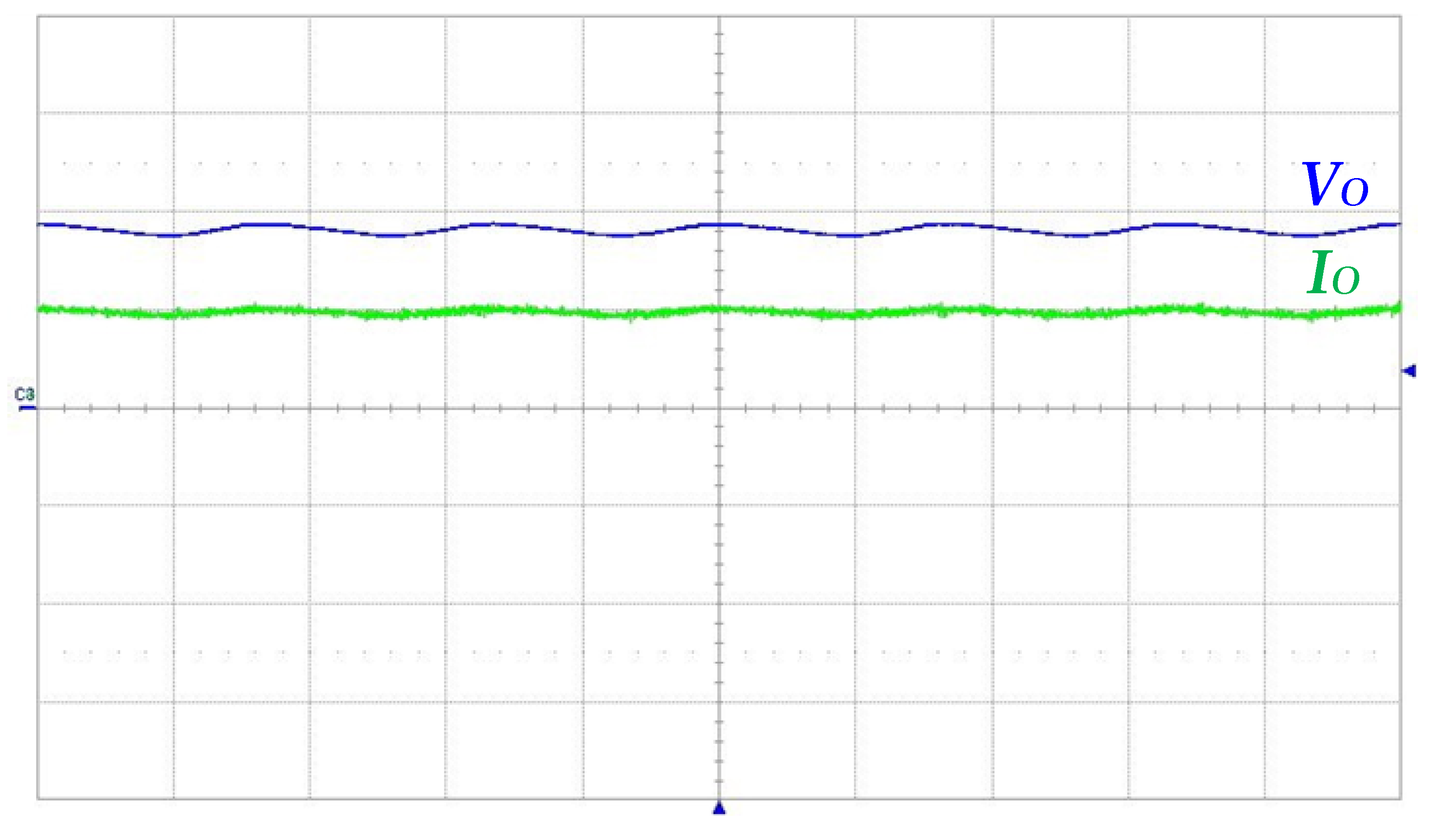
Figure 13 illustrates the measured output voltage
VO and output current
IO, with corresponding average values of 36.2 V and 2.0909 A. The peak-to-peak variations in the output voltage and current are observed to be 3.5114 V and 0.2346 A, respectively. Based on these measurements, the ripple factors—defined as the ratio of the peak-to-peak value to the average value—are calculated to be 9.7% for the output voltage and 11.22% for the output current.
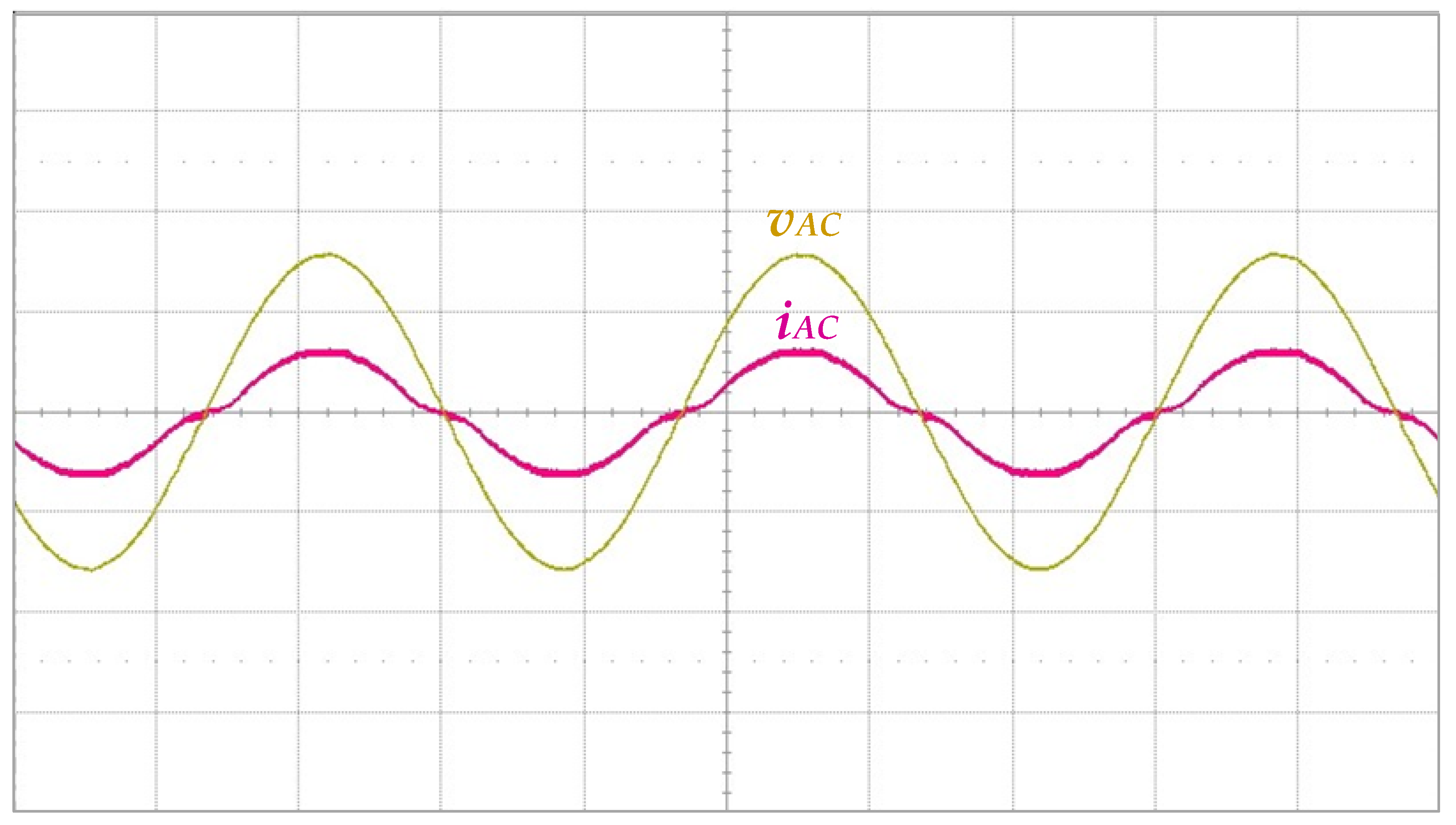
Figure 14 presents the input utility-line voltage (
vAC) and input current (
iAC). It can be observed that the input current waveform closely follows the voltage waveform, thereby demonstrating the power factor correction (PFC) capability of the proposed isolated LED electronic lighting driver circuit.
Table 3 summarizes the harmonic components of the input current, obtained from measurements conducted with a power analyzer under a 110 V AC input condition. These measured values are compared with the IEC 61000-3-2 Class C standard limits [
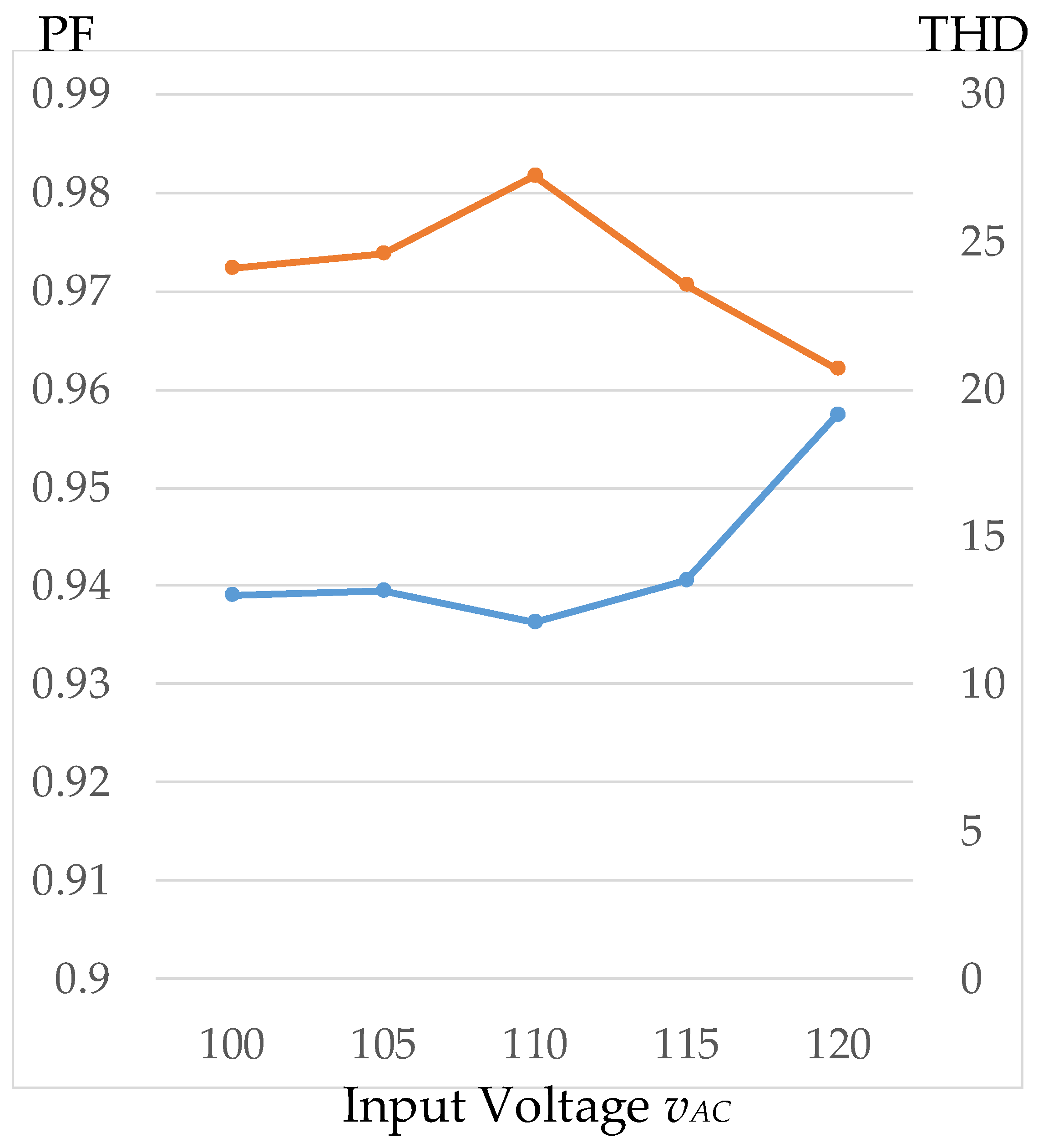
31]. The proposed driver circuit achieves a power factor of 0.9816 and a total harmonic distortion (THD) of 12.094%. Additionally, the overall conversion efficiency of the prototype LED driver was measured to be 82.3%.
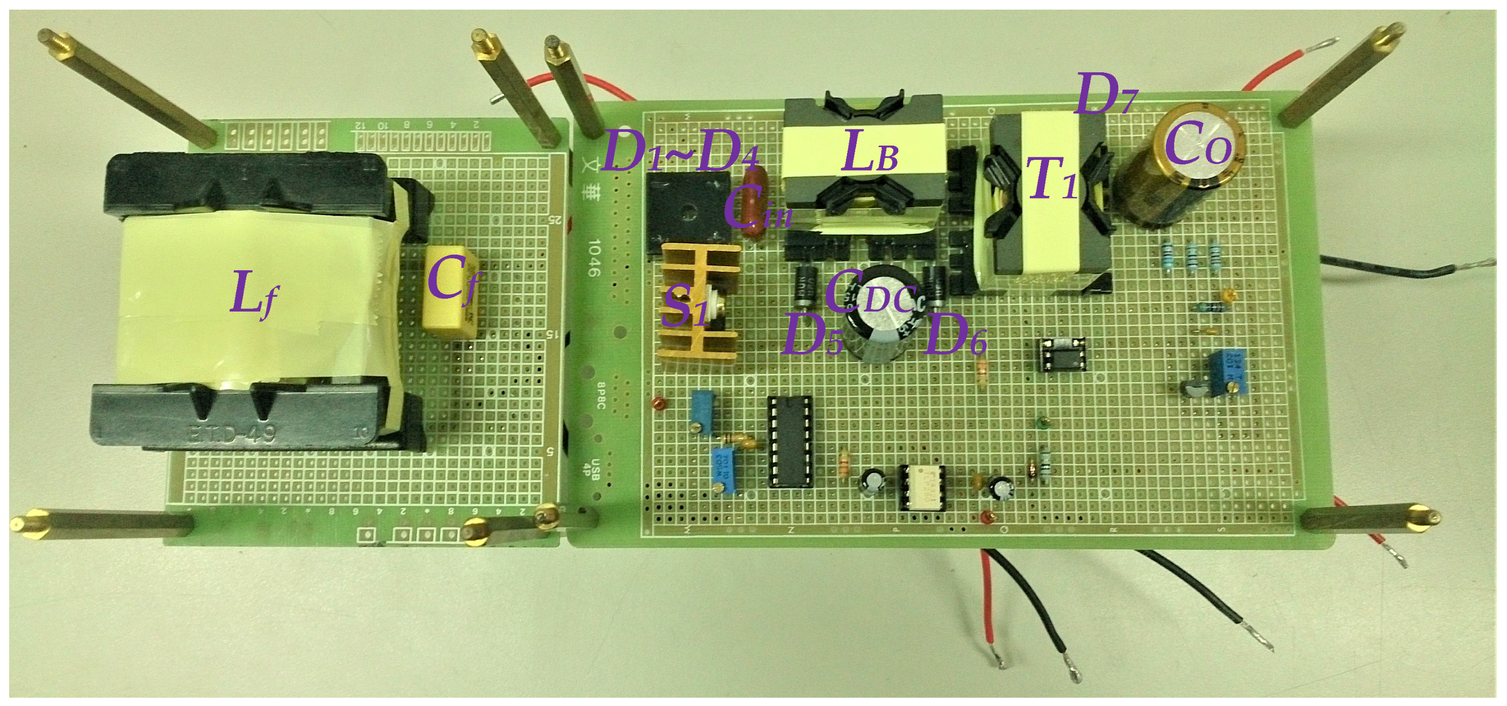
Figure 15 shows a photograph of the clear top-view schematic of the prototype AC-DC electronic lighting driver circuit.
Figure 16 presents a photograph of the prototype AC-DC electronic lighting driver circuit with power factor correction used to power LEDs applied to an AC input voltage source with a value of 110 V rms. In addition, the input AC current harmonics, power factor, and total harmonic distortion of the prototype electronic lighting driver circuit were tested and measured at input voltages ranging from 100 V to 120 V.
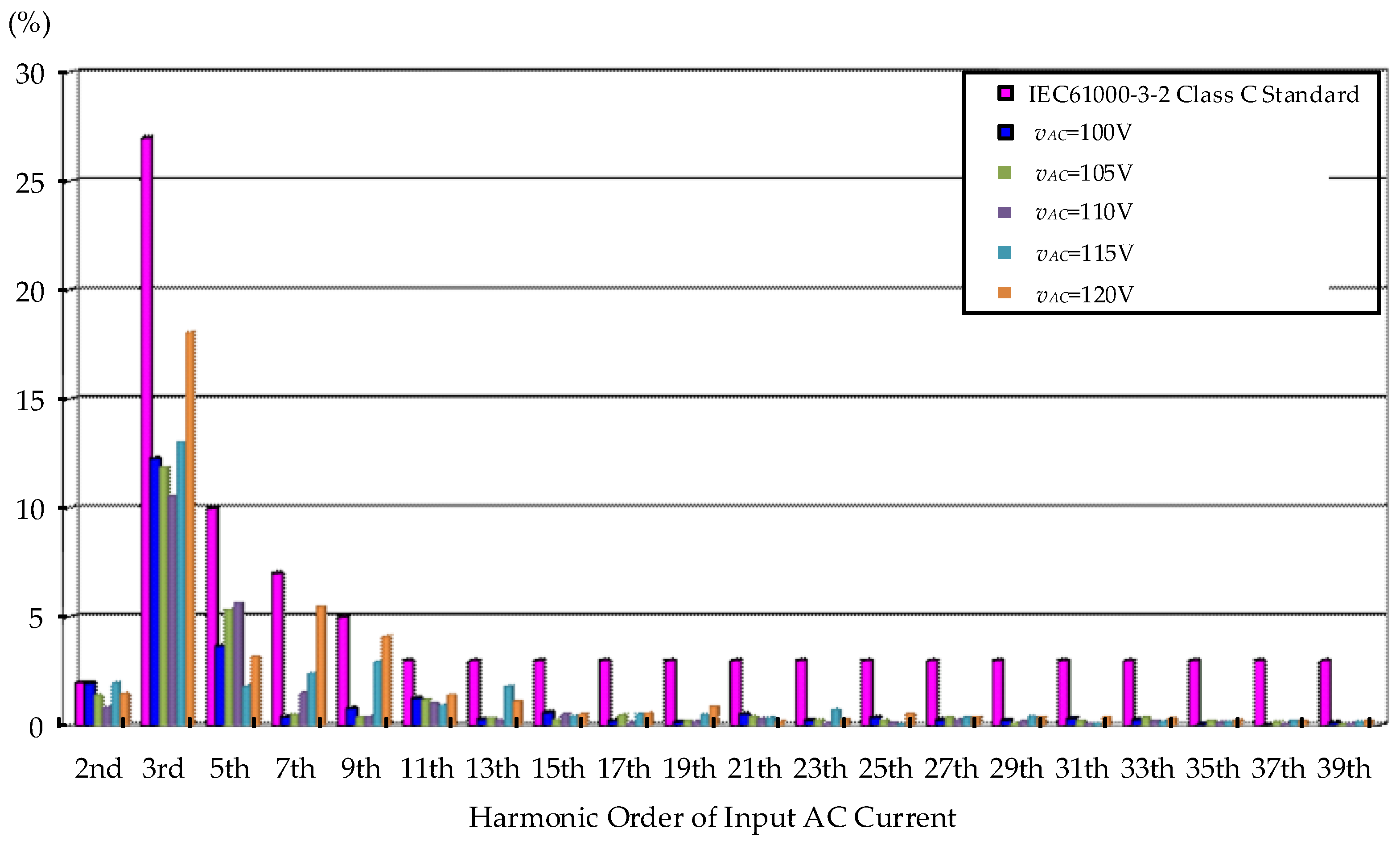
Figure 17 presents the measured values of input AC current harmonics at each input AC voltage and their comparison with the IEC 61000-3-2 Class C standard.
Figure 18 shows the power factor and total harmonic distortion of current measured for the prototype electronic lighting driver circuit at different input AC voltages.
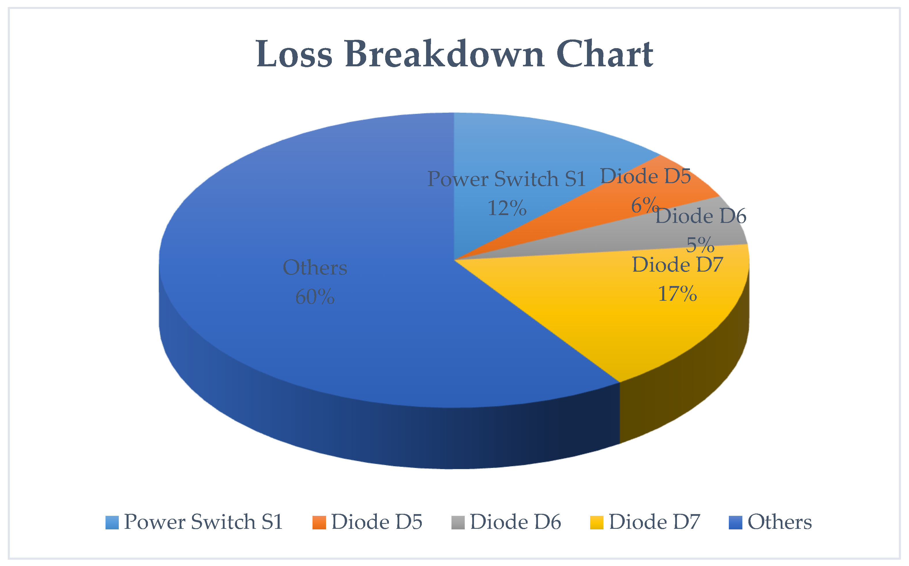
Figure 19 illustrates the detailed power loss distribution of the prototype isolated LED electronic driver circuit incorporating power factor correction, thereby serving as empirical support for the efficiency metrics presented in this study. As shown, the individual contributions to the overall power loss by critical circuit components are quantified as follows: the power switch
S1 accounts for 12% of the total losses, diode
D5 contributes 6%, while diodes
D6 and
D7 are responsible for 5% and 17%, respectively. The remaining 60% of the total power loss is attributed to various other circuit elements and parasitic phenomena. This comprehensive breakdown offers valuable insight into the primary sources of inefficiency within the driver architecture and identifies key areas where future design improvements may be directed to enhance overall performance.
Table 4 provides a comparative analysis of the proposed AC-DC LED driver circuit against two previously reported designs. The first reference [
32] describes a 100 W (36 V/2.77 A) driver comprising a modified stacked dual-boost converter integrated with a half-bridge LLC resonant converter, operating from a 110 V AC input. The second design [
33] employs an inverted buck-boost converter with a lossless snubber, delivering 18 W (60 V/0.3 A) from the same input voltage. In contrast, the proposed driver circuit utilizes a modified flyback converter integrated with a lossless snubber to achieve an output power of 72 W (36 V/2 A).
Compared to the topology in [
32], the proposed design reduces component count by eliminating one power switch, two power diodes, and one magnetic component, thereby offering a more compact and potentially cost-effective solution. However, the circuit in [
32] demonstrates superior efficiency due to the implementation of soft-switching techniques and exhibits lower total harmonic distortion (THD) in the input current, as well as better current quality.
In comparison with the design in [
33], the proposed circuit requires an equivalent number of components, while achieving a measured efficiency above 82%, similar to both referenced designs. Notably, the proposed driver achieves a higher power factor than the topology in [
33], along with a reduced input current THD, signifying enhanced power quality performance.
5. Conclusions
This study presents the design and implementation of an isolated AC-DC LED electronic lighting driver circuit with integrated power factor correction, intended for operation from an AC input voltage source. The proposed topology is based on a modified flyback converter combined with a lossless snubber circuit, which effectively recovers the leakage inductance energy, thereby improving overall efficiency. A 72 W-rated prototype was developed to drive LED loads with an output voltage of 36 V and output current of 2 A under a 110 V AC input condition. Experimental validation confirms that the proposed driver achieves a high-power factor exceeding 0.98 and a low total harmonic distortion (THD) of the input current below 13%. Moreover, all measured input current harmonics comply with the IEC 61000-3-2 Class C standard, demonstrating the suitability of the proposed design for practical and regulatory-compliant LED lighting applications.
In summary, the implemented prototype driver circuit, which integrates a modified flyback converter with a lossless snubber and inherent PFC capability, achieves an overall efficiency of 82.3%. While this efficiency is somewhat lower than that reported for state-of-the-art LED driver technologies—particularly those employing soft-switching strategies—the proposed design nonetheless demonstrates significant advantages. By minimizing the component count, the circuit attains a more compact structure and offers the potential for reduced manufacturing costs. These characteristics highlight the practical relevance of the proposed approach and suggest its suitability for applications where cost-effectiveness and compactness are prioritized over maximum efficiency. Future work will focus on further enhancing the efficiency of the design while preserving its structural simplicity and economic feasibility.
Additionally, the implementation of dimming functionality in the proposed isolated AC-DC LED electronic driver circuit represents another potential direction for future work. This functionality can be achieved by incorporating an additional power switch in series with the LED load. By employing pulse-width modulation (PWM) control, the dimming operation is facilitated through the adjustment of the duty cycle of the supplementary switch. This approach enables modulation of the average current supplied to the LEDs, thereby achieving effective and precise brightness control.
