1. Introduction
The increasing deployment of residential and distributed Photovoltaic (PV) systems has intensified the need for high-efficiency and cost-effective power conversion architectures. These systems operate under variable environmental and load conditions, which introduce nonlinearities into the electrical behavior of PV modules and necessitate real-time adaptation of the operating point to track the maximum power point [
1,
2]. This critical function is typically handled at the DC-DC conversion stage, where both energy transfer and regulation tasks converge.
DC-DC converters represent a fundamental component in PV energy systems, as they interface directly with the source and execute Maximum Power Point Tracking (MPPT) algorithms. A variety of topologies have been investigated for this purpose, including boost, buck-boost, interleaved, and coupled-inductor configurations, each offering distinct advantages in terms of voltage gain, component stress, and conversion efficiency. In addition to tsopology, the control strategy employed plays a decisive role in ensuring system robustness and dynamic response. In recent years, Sliding Mode Control (SMC) techniques have gained prominence due to their robustness to parameter uncertainties and external disturbances, offering fast convergence and accurate current tracking in power converters [
3,
4].
Beyond traditional full-power designs, recent research has explored the use of Partial-Power Processing (PPP) architectures, in which only a fraction of the total load power is processed by the converter. These topologies, such as the Input-Parallel Output-Series (IPOS) configuration analyzed in this paper, enable significant reductions in converter size, thermal stress, and power losses, thereby increasing global system efficiency. PPP converters are especially promising for PV systems, where the voltage and current profiles allow for effective partial processing without compromising control performance. This work presents a novel non-isolated buck-boost-based PPP architecture with dual-loop PI–SMC control, designed to enhance efficiency and stability under variable operating conditions and validated through both simulation and Hardware-in-the-Loop (HIL) implementation.
In recent years,
Sliding Mode Control (
SMC) has emerged as a powerful alternative to classical control techniques—such as
PI or
PID—for DC-DC power converters due to its robustness against model uncertainties, parameter variations, and external disturbances [
5]. Unlike linear controllers, which often struggle under nonlinear or time-varying dynamics, SMC ensures finite-time convergence and high disturbance rejection, making it particularly suited for photovoltaic systems operating under rapidly changing environmental conditions. Various advanced SMC strategies have been explored to improve system performance: non-singular terminal SMC with extended state observers for uncertainty compensation and chattering reduction [
6]; adaptive SMC schemes tuned via metaheuristic optimization for enhanced dynamic response [
7]; and hyperbolic tangent sliding functions to smooth control actions and reduce switching noise [
8]. Other works focus on digital implementations using FPGA for real-time control [
9] or discrete-time formulations with disturbance estimators to tackle mismatched uncertainties [
10]. The integration of SMC in converters with input filters and constant power loads has also shown effectiveness in stabilizing oscillatory behaviors [
11]. Despite its advantages, SMC can introduce chattering phenomena and requires careful design of the sliding surface and switching logic. Nevertheless, the wide range of enhancements proposed in the literature reflects its strong potential for robust control in high-performance and real-time PV energy systems.
In this context, the present work addresses several of the gaps identified in the prior literature. Specifically, it introduces a partial-power DC-DC converter [
12] with a
PI–SMC control scheme, emphasizing both the control performance [
13] and the power processing efficiency under dynamically variable conditions [
14]. Unlike prior studies, the proposed system includes an integrated evaluation of current and voltage regulation, power transfer efficiency, and converter stability, all validated through real-time hardware simulation. This holistic approach contributes a novel and practical perspective on the design and assessment of robust
MPPT controllers for PV systems.
The Partial-Power Converter (PPC) paradigm has gained attention as an effective strategy to increase energy efficiency and reduce stress on power components in applications such as PV systems [
15,
16], electric vehicle chargers [
17,
18], active power-buffer in fuel-cell [
19], and high-density data centers [
20]. The reviewed literature reveals a broad spectrum of topologies—ranging from non-isolated
Cuk-based stages [
21] to isolated full-bridge and resonant designs—each tailored to specific constraints of power density, scalability, and modularity. Main innovations include reconfigurable architectures, flux cancellation techniques [
22], hybrid control strategies, and topology adaptation [
23,
24] to reduce the processed power ratio [
17] and improve thermal performance. Many works report efficiencies exceeding 98%, with some surpassing 99.5% [
18,
25], and significant reductions in power stage ratings [
20]. Additionally, several studies [
26,
27] validate their proposals through experimental or real-time simulation platforms [
28]. These contributions reinforce the versatility of PPC architectures and motivate their integration in next-generation renewable energy systems and high-performance conversion platforms [
17,
29].
In light of the reviewed developments, this work presents a novel PV-oriented converter architecture based on a non-isolated buck-boost topology with Partial-Power Processing (PPP). The converter is regulated by a dual-loop control scheme combining a Proportional–Integral (PI) voltage regulator with an inner Sliding-Mode Controller (SMC) for current tracking (Dual PI–Sliding Mode Control). This configuration enables accurate regulation while minimizing the processed power, thus reducing component stress and improving overall energy efficiency. The system is validated through both MATLAB-Simulink simulation and real-time Hardware-in-the-Loop (HIL) implementation using the OPAL-RT platform. The results confirm the architecture’s suitability for scalable, robust, and cost-efficient deployment in modern distributed PV systems and DC microgrids.
Table 1 and
Table 2 summarize recent developments in DC-DC converter architectures and control strategies applied to photovoltaic systems, respectively. These comparative references help position the proposed converter topology and dual-loop control scheme within the context of existing works.
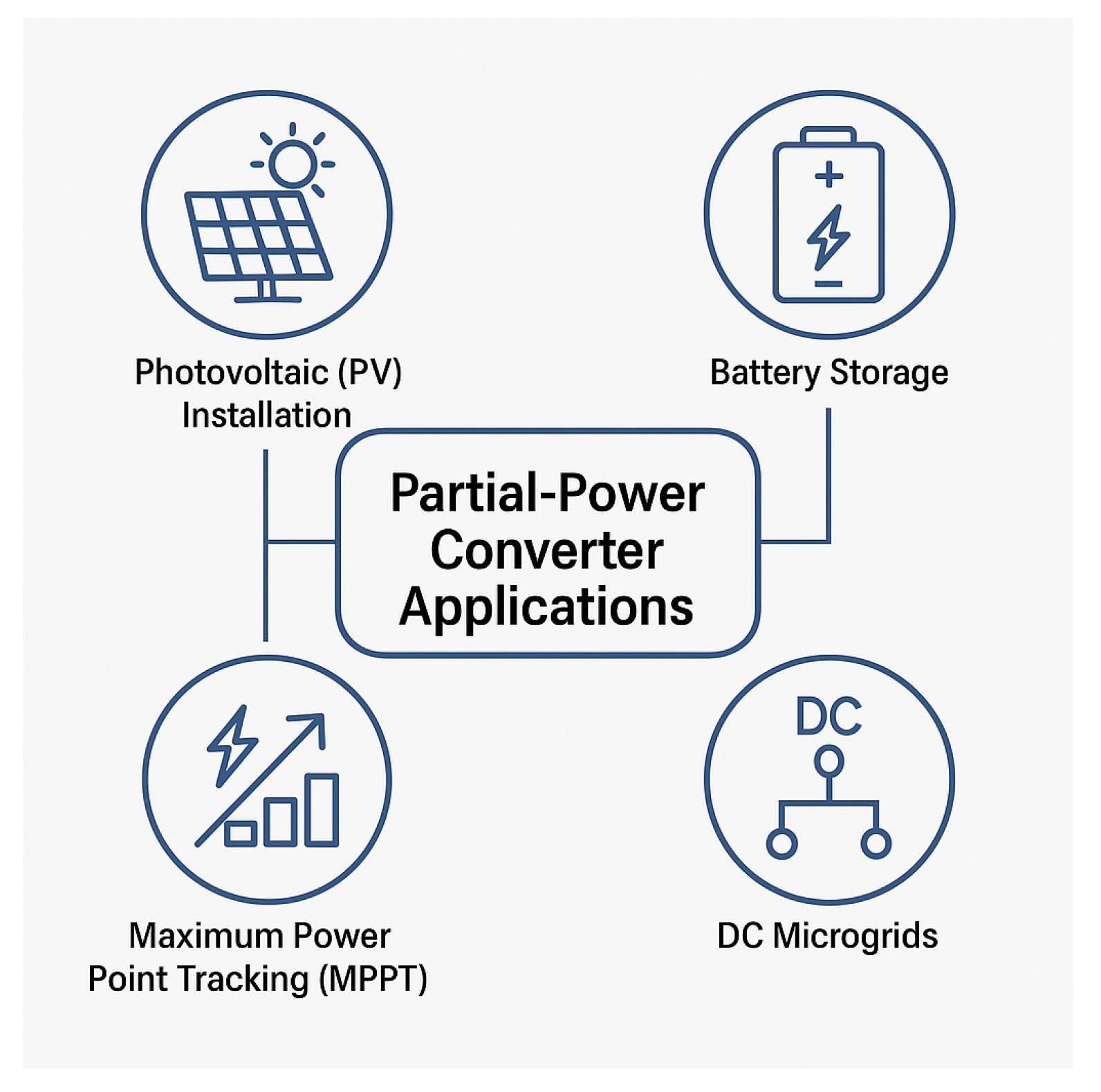
Partial-power converter architectures have emerged as a promising solution for high-efficiency power management in renewable energy systems. Their defining feature—the ability to process only a fraction of the total power—enables reduced conduction losses, improved thermal performance, and lower component stress compared to full-power topologies. These advantages make them particularly attractive for a wide range of applications, including Photovoltaic (PV) installations, battery energy storage systems, Maximum Power Point Tracking (MPPT), and DC microgrids, see
Figure 1.
In PV arrays, partial-power converters facilitate efficient MPPT implementation by allowing for direct energy transfer through a passive path while regulating only the required portion of the power, thereby enhancing energy harvesting. In storage interfaces, their bidirectional operation improves round-trip efficiency while preserving component lifespan. Furthermore, when deployed in modular or series-stacked system architectures, they offer inherent scalability and contribute to distributed thermal management. Nevertheless, their performance can be affected by variations in the input–output voltage ratio, especially under wide dynamic conditions. This necessitates the use of robust and well-coordinated control strategies to ensure stability, accurate power regulation, and proper interaction with the passive power flow. Despite these considerations, partial-power converters present a highly effective and scalable alternative for modern, cost-sensitive renewable energy applications where moderate voltage conversion is acceptable.
To address the aforementioned ideas and propose an efficient alternative for PV power processing, this paper presents the design, control, and validation of a partial-power converter regulated through a dual-loop
PI–Sliding Mode Control strategy. This document is organized as follows.
Section 1 provides a contextual introduction, including the motivation, state-of-the-art review, and identification of current limitations in MPPT and converter topologies.
Section 2 presents the theoretical foundation and dynamic behavior of the proposed partial-power converter, highlighting its operating modes and characterizing the system’s power ratio and voltage gain in relation to the duty cycle.
Section 3 describes the full configuration of the PV-converter system, including component modeling, power flow equations, and relevant operating constraints under realistic irradiance and load profiles.
Section 4 develops the control architecture, detailing the design of a PI controller for voltage regulation and a Sliding-Mode Controller (SMC) for inductor current tracking. The section also discusses the advantages and practical considerations of implementing SMC in power converters.
Section 5 presents simulation results under dynamic conditions, along with a real-time implementation using the
OPAL-RT platform to evaluate the system’s performance in hardware-oriented scenarios. Comparative results validate the accuracy and robustness of the proposed approach. Finally,
Section 6 summarizes the main contributions of the work and outlines potential directions for future developments in partial-power control systems for PV applications.
2. Dynamic Behavior and Operation Modes of Partial-Power Converter
As a novelty, the architecture under study is a bidirectional, non-isolated partial-power DC-DC converter derived from the classical buck-boost topology. This converter is integrated into a series configuration with the load, allowing only a fraction of the total power to be processed by the converter itself. Such an arrangement significantly enhances overall system efficiency, reduces converter size, and lowers thermal stress on power components. This partial-power processing architecture is being studied for higher power renewable energy applications [
12,
17]. Unlike general treatments of buck-boost converters, this section introduces a partial-power architecture with modified gain and impedance behavior. The theoretical analysis focuses on steady-state and power flow modeling in to Input-Parallel Output-Series (IPOS) configurations.
Figure 2 illustrates the fundamental difference between conventional full-power converter architectures and the proposed partial-power configuration. In a full-power system, the entire energy flow from the DC source to the load is processed through the converter stage, which must handle 100% of the power, leading to increased conduction losses, larger component sizing, and higher thermal stress. In contrast, the partial-power architecture connects the DC-DC converter in series with the load—either at its input or output terminal—such that only a fraction of the total power is actively processed by the converter. This structure, typically referred to as an Input-Parallel Output-Series (IPOS) configuration, enables a significant portion of the power to bypass the active stage, flowing passively from the source to the load. As a result, the converter operates with reduced power handling requirements, which translates into higher overall system efficiency, improved thermal performance, and potential reductions in cost and size of the power processing unit.
In the full-power topology, the converter processes all the power flow supplied to the load from the DC-bus (
+vDC). Thus, the converter output voltage (
vO) is equal to the load voltage (
vLD (
vO =
vLD)). Whereas, in the partial-power topology, the load is connected in series between the DC-bus and the input or output of the DC converter, see
Figure 2.
In the proposed Partial-Power Processing (PPP) topology, the converter is arranged in a series configuration with the load, following an Input-Parallel Output-Series (IPOS) topology [
15], which minimizes the converter’s processed power, enabling higher efficiencies, especially in high-power applications such as photovoltaic systems or electric mobility [
19]. This structural arrangement leads to a split in the total power delivered to the load: a portion flows directly from the DC source through the passive path, while the remainder is regulated by the DC-DC converter. The voltage relationship at the load node can be written as follows:
where
vLD is the load voltage (DC-bus),
vIN =
vDC is the input voltage from the source (e.g., photovoltaic panel
vpv),
vO is the output voltage of the converter (
vC), and
Mf is the gain of the buck-boost converter as a function of the duty cycle (
D). This relationship guarantees that the load voltage (
vLD) is always greater than the source voltage, aligning with the requirements of step-up operations commonly seen in renewable energy systems (
vDC) [
21]. Consequently, the converter gain (
Mf) and the system gain (
M) can be defined as follows:
This expression highlights the additive voltage behavior inherent to the IPOS configuration and sets the basis for modeling the converter’s role in partial-power handling. The processed power ratio, a key metric for evaluating efficiency, is defined as follows:
This parameter directly quantifies the fraction of power managed by the converter. It decreases as the converter output (vC2) (and thus Mf) becomes smaller relative to the total load voltage (vLD), confirming that efficiency improves when most of the power is transferred passively. This analytical framework defines the operational principle of the converter and supports the subsequent modeling of steady-state and dynamic performance.
Unlike traditional boost converters, which often suffer from severe efficiency drops due to high duty cycles, current ripple, and component stress, the partial-power converter can achieve similar or better output performance while handling significantly less power internally [
31]. This results in reduced thermal losses, increased reliability, and lower costs.
Figure 3 depicts the power flow distribution in the partial-power setup, clearly indicating that only a controlled portion of power passes through the converter stage [
21]. The introduction of new partial-power processing topologies allows us to develop smaller and cheaper DC-DC converters, while power losses are reduced. In this paper, some advantages of the partial-power architecture on renewable energy applications have been verified.
Table 3 summarizes the main differences between traditional full-power converter architectures and the proposed partial-power approach. As shown, the partial-power solution introduces significant advantages in terms of efficiency, size, cost, and reliability, making it particularly attractive for renewable energy applications such as photovoltaic and storage-based systems.
To quantitatively assess the benefits of the partial-power processing approach, the
processed active power ratio (
kPR) is introduced. This parameter represents the proportion of power actively processed by the converter relative to the total power supplied by the source, and is defined as follows:
For the converter to operate effectively in the partial-power mode, the condition kPR < 1 must be satisfied. This implies that only a fraction of the total power is handled by the converter, while the remaining power is directly delivered to the load through the passive path. In this way, the partial architecture will be more feasible, compared to the conventional option, when the reference parameter kPR is lower.
By applying Kirchhoff’s voltage law to the series-connected architecture, the relationship between
kPR and the static voltage gain (
GvPPC) is derived as follows:
where
ηsystem is the overall system efficiency. Assuming an ideal converter (
ηconverter ≈ 1, it is possible due to the high efficiency of DC-DC converters), this equation shows that when the voltage gain approaches unity (i.e., input and output voltages are similar), the power processed by the converter is minimized.
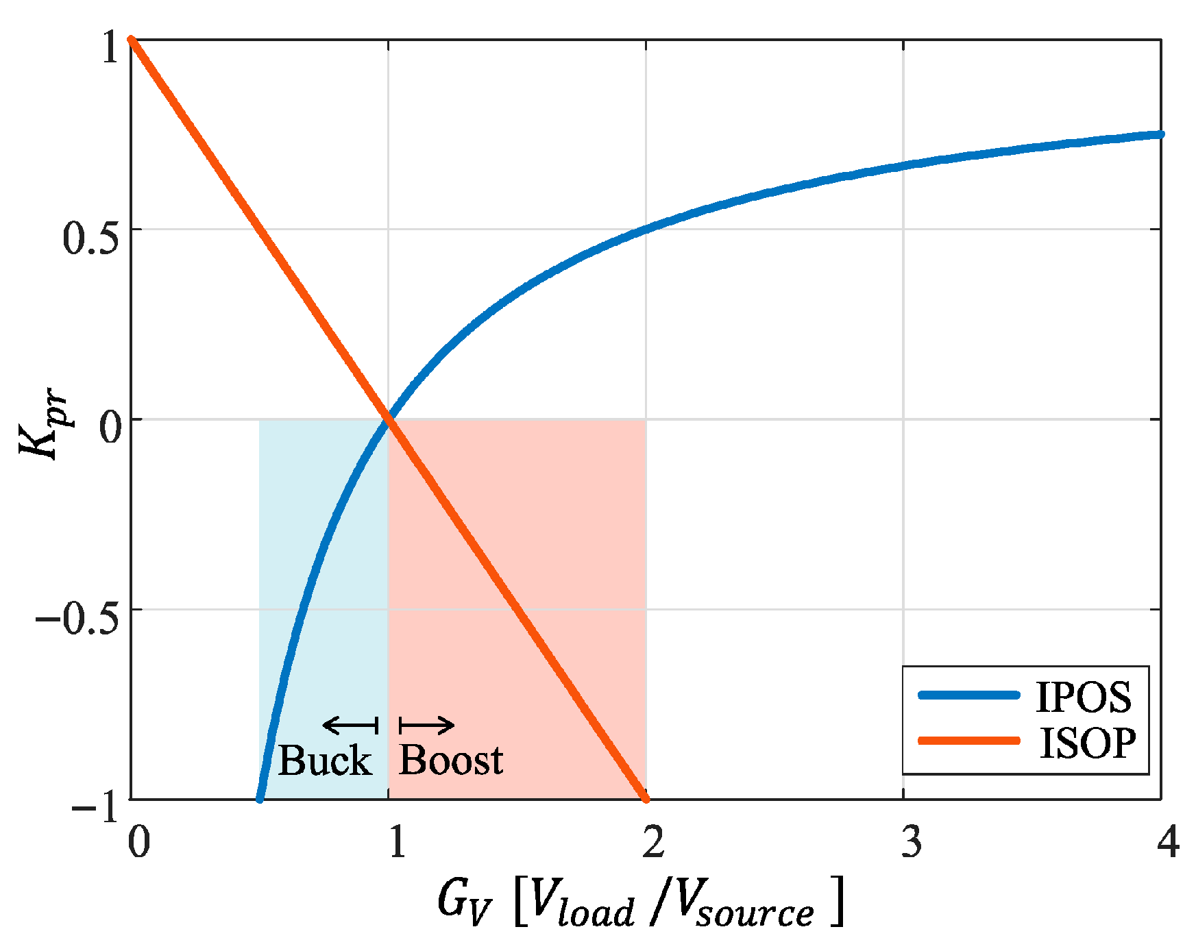
Figure 4 presents the characteristic curves of the power processing ratio (
kPR) as a function of the static voltage gain for both step-up (
IPOS) and step-down (
ISOP) partial-power topologies. These curves demonstrate that partial-power converters offer their greatest performance advantages in scenarios where the voltage difference between the input and the load is relatively small. Under such conditions, the converter processes only a minimal fraction of the total power, resulting in enhanced system efficiency and reduced stress on active components.
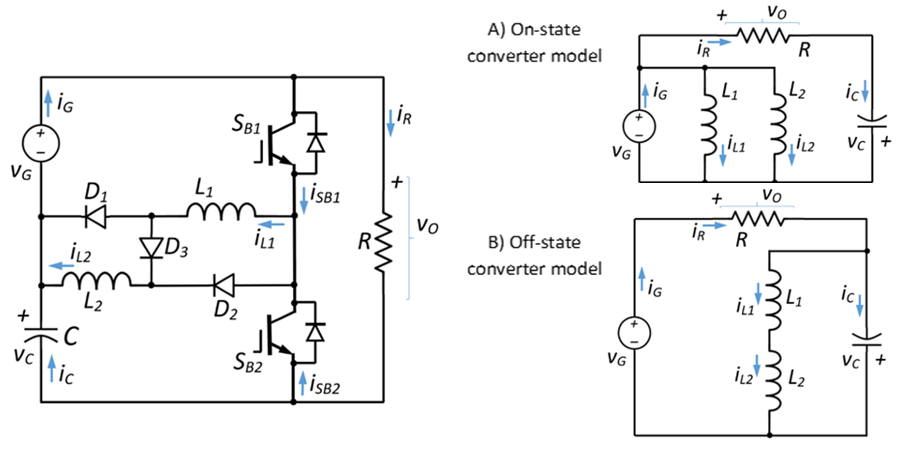
In order to simplify the steady-state analysis of the proposed architecture, some assumptions are made, such as ideal inductors and switching devices without delay in the switching process (see
Figure 5). Thus, for the
TSW switching time, the switch is ON for
D ×
TSW time while OFF for (1 −
D) ×
TSW time. Therefore, depending on the state of the switch, two modes of operation in the continuous conduction mode (
CCM) can be identified. The following is considered as an initial assumption:
In this way,
At the initial time
t = 0, when switch
S1 turns on, diode
DS2 turns off. As a consequence, the diodes
D1 and
D2 are in conduction, while
D3 remains in cut, and the inductor currents (
iL1 and
iL2) increase from their respective initial values. In this case, the voltage and current equations are as follows:
When switch
S1 turns off (
t = D ×
TSW),
DS2 becomes forward-biased. Diodes
D1 and
D2 are now off, while
D3 conducts. The voltage and current dynamics in this interval are as follows:
For steady-state operation, the average inductor voltage (
vL) over a switching period must be zero. Therefore, analyzing the
volts–second balance for the inductors (
L) during a
TSW switching period, we obtain the following:
Solving for
vC (capacitor voltage) and substituting the following:
The input voltage (
vG) is assumed to be constant over a switching period, thus solving for the steady-state output voltage
vO as follows:
This expression highlights the step-up characteristic of the buck-boost-based partial-power converter. The instantaneous duty cycle
D(
t) can be expressed as a function of
vG and
vO, as follows:
In addition, the average capacitor current (
vC) should be zero at the steady state. In this way, analyzing the current–second balance for the capacitor (
C), during a
TSW switching period, we obtain the following:
The input current (
iG) supplied by the DC source (
vG) can be written as follows:
Substituting the previous results, the following is obtained:
These equations show how the converter dynamically distributes power between the passive path and the active converter stage. The reduction in converter-handled current leads to substantial decreases in conduction losses.
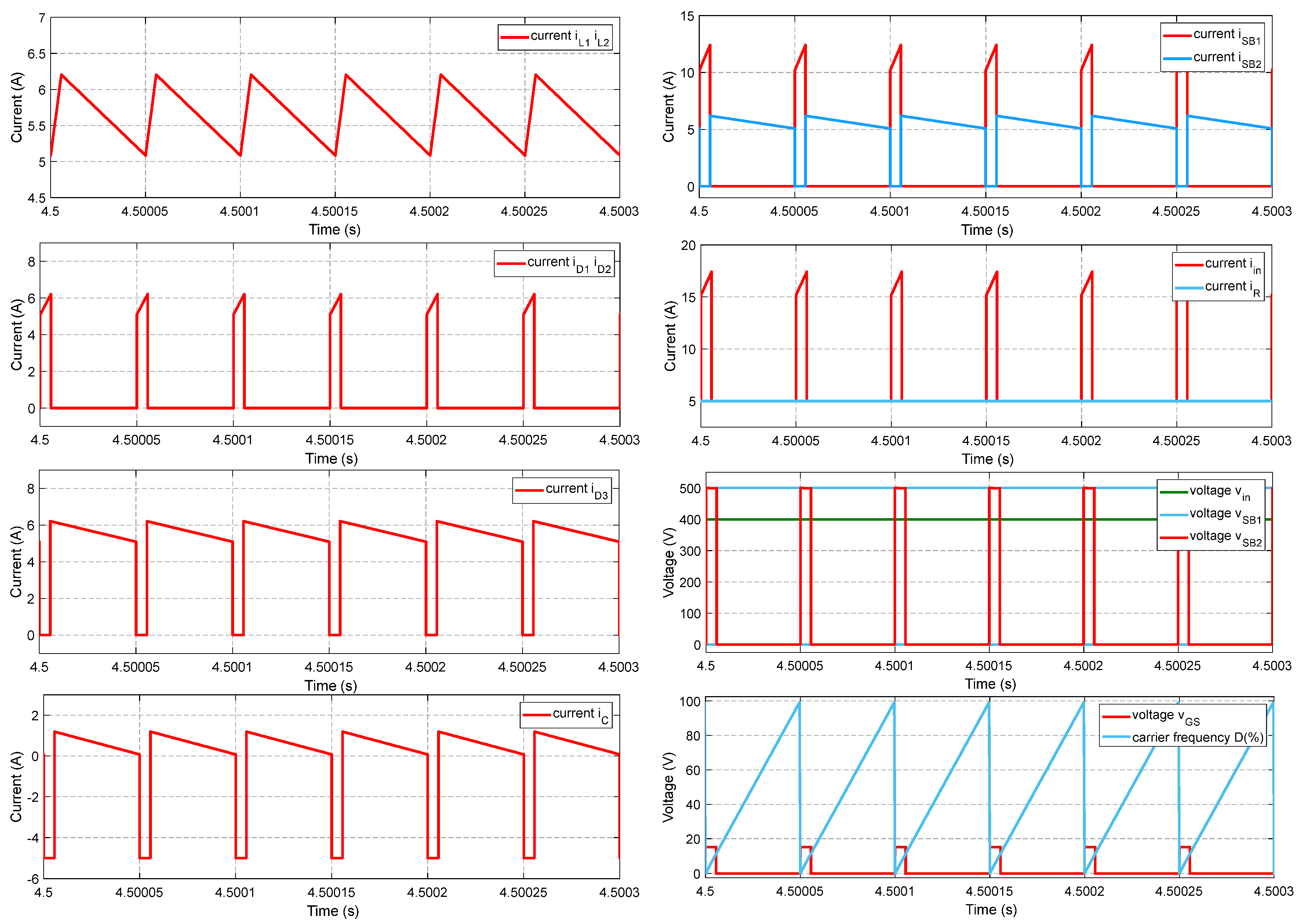
Figure 6 presents the simulation waveforms of the proposed converter using
MATLAB-Simulink R2024b. It includes the current and voltage profiles of all key components, such as the inductor currents (
iL1 and
iL2), diode currents (
iD1,
iD2, and
iD3), source current (
iG), capacitor current (
iC), or simply the load current (
iR). In the analyzed scenario, an input voltage of
vG = +400 V, a duty cycle of
D = 11.11%, and output voltage of
vO = +500 V have been considered. The load resistance (
R) is set accordingly to achieve steady-state operation.
The plots confirm that the converter operates in the intended partial-power mode, with a reduced current stress on the switching devices and predictable voltage conversion behavior. These simulations validate both the dynamic model and the theoretical relationships derived above.
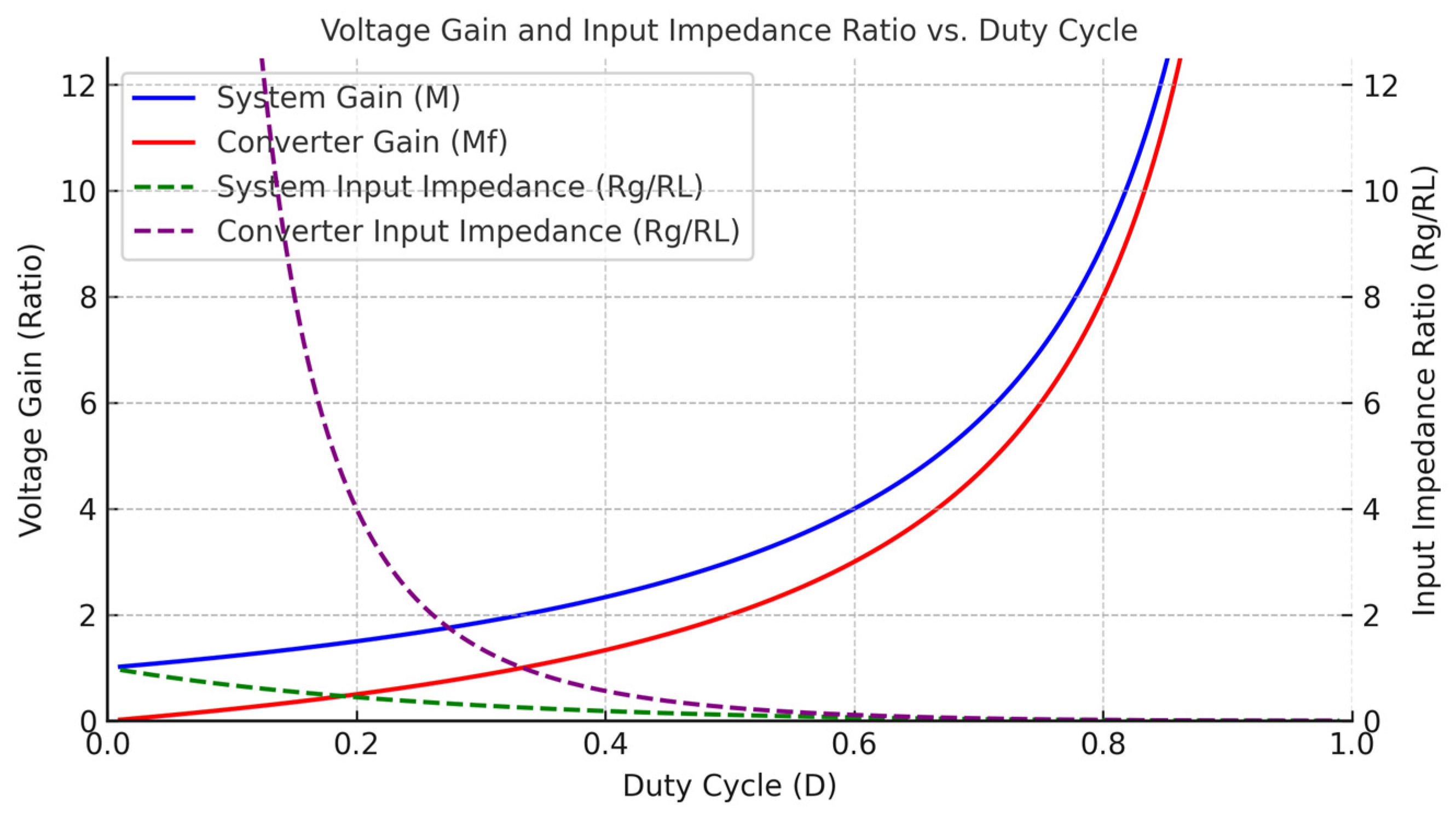
The relationship between the duty cycle (
D), converter gain (
Mf = vC2/vpv), and total system gain (
M = vO/vpv) can be analytically derived from the operating principles of the series-connected partial-power architecture. Considering the converter output voltage (
vC2) in terms of
D, the gain of the converter is defined as follows:
Given that the system output voltage is the sum of the PV input and the converter output voltages (
vO =
vpv +
vC2), the system gain becomes the following:
In partial-power converter architectures, particularly in Input-Parallel Output-Series (IPOS) configurations, the input impedance seen from the source plays a key role in defining system stability, dynamic performance, and energy transfer capability. A proper impedance profile ensures that the source operates under favorable loading conditions, avoiding excessive current stress or inefficient operating points. For the proposed topology, the following two impedance perspectives must be distinguished: the equivalent input impedance of the overall system and the intrinsic input impedance of the converter stage.
The normalized input impedance of the system (
RG), referred to as the load resistance (
RL), can be expressed as follows:
This expression accounts for the power flow partially bypassing the converter and highlights the decrease in effective impedance as the duty cycle increases. On the other hand, the input impedance referred only to the converter stage is given by the following:
which reveals a more rapid decrease in impedance for an increasing
D. These relationships are fundamental for assessing the interaction between the source and the converter and must be considered when selecting operating ranges or designing upstream PV or energy-harvesting subsystems. In particular, excessive impedance mismatches at high duty cycles may deteriorate voltage regulation and dynamic response, especially under variable irradiance or load transients.
Figure 7 presents a comprehensive analysis of the converter’s behavior by plotting both the voltage gain and input impedance ratio as functions of the duty cycle (
D). The system voltage gain (
M) and the converter voltage gain (
Mf) increase nonlinearly with
D, maintaining a constant offset between them (
M = Mf + 1). This relationship is inherent to Input-Parallel Output-Series (IPOS) topologies, where the output voltage results from the additive contribution of a passive and an actively regulated power path. The figure also includes the normalized input impedance ratio (
RG/RL) for both the system and the converter stage, showing a smooth or steep decline, respectively, as
D increases. These profiles illustrate how duty-cycle modulation affects source loading and converter stress.
The detailed analysis of the dynamic behavior and operational principles of the partial-power converter confirms its suitability for high-efficiency renewable energy applications. The following section addresses the experimental validation and performance assessment under real-world operating conditions. Future developments may focus on enhancing dynamic performance through advanced control strategies, adaptive duty-cycle modulation, and seamless integration with intelligent MPPT algorithms to further optimize energy conversion under variable operating conditions.
3. System Description
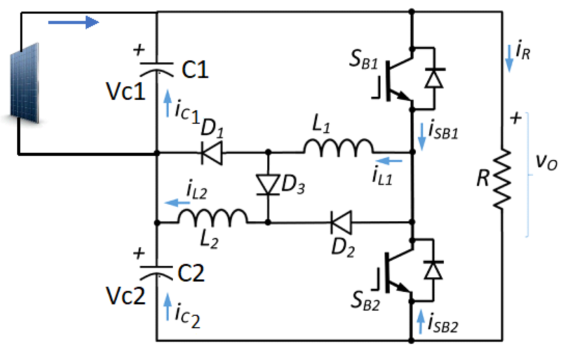
The overall configuration of the PV partial-power converter system is depicted in
Figure 8, based on the topology presented in [
4]. The system integrates a photovoltaic (PV) array composed of four modules, connected to a two-stage single-phase inverter. The first stage consists of an improved DC-DC buck-boost converter, which is responsible for executing maximum power point tracking (
MPPT). The second stage is an inverter that converts the regulated DC voltage into AC, which is subsequently applied to the load through an
LC output filter.
Figure 8 illustrates a schematic diagram of the system, highlighting key components:
C1 and
C2 are the intermediate capacitors that provide voltage stabilization and energy buffering;
L1 and
L2 are inductors used in the converter; the resistive load (
R) is used to simulate the current injection into the DC-bus, effectively emulating a real power system interconnection. The signal
u (1, 0) represents the discrete-time control input of the step-up stage, while
S1 and
S2 are the active switching devices. This operating principle is further detailed through differential Equations (29)–(31), which describe the dynamic evolution of the inductor and capacitor voltages under PWM modulation. These relationships serve as the basis for the subsequent control design.
The dynamic behavior of the system is described by the following set of differential equations:
where
iPV denotes the current generated by the PV array,
iL denotes the current flowing through the equivalent inductor, as defined in the simplified model shown in
Figure 4, and
vC is the voltage across capacitor (
C1), which also defines the operating point of the PV system. Likewise,
vC2 is the voltage across capacitor
C2, determining the DC-link voltage delivered to the inverter (
vO =
vC1 +
vC2). The signal
u is a binary control variable (either 0 or 1) that governs the switching state of the buck-boost converter.
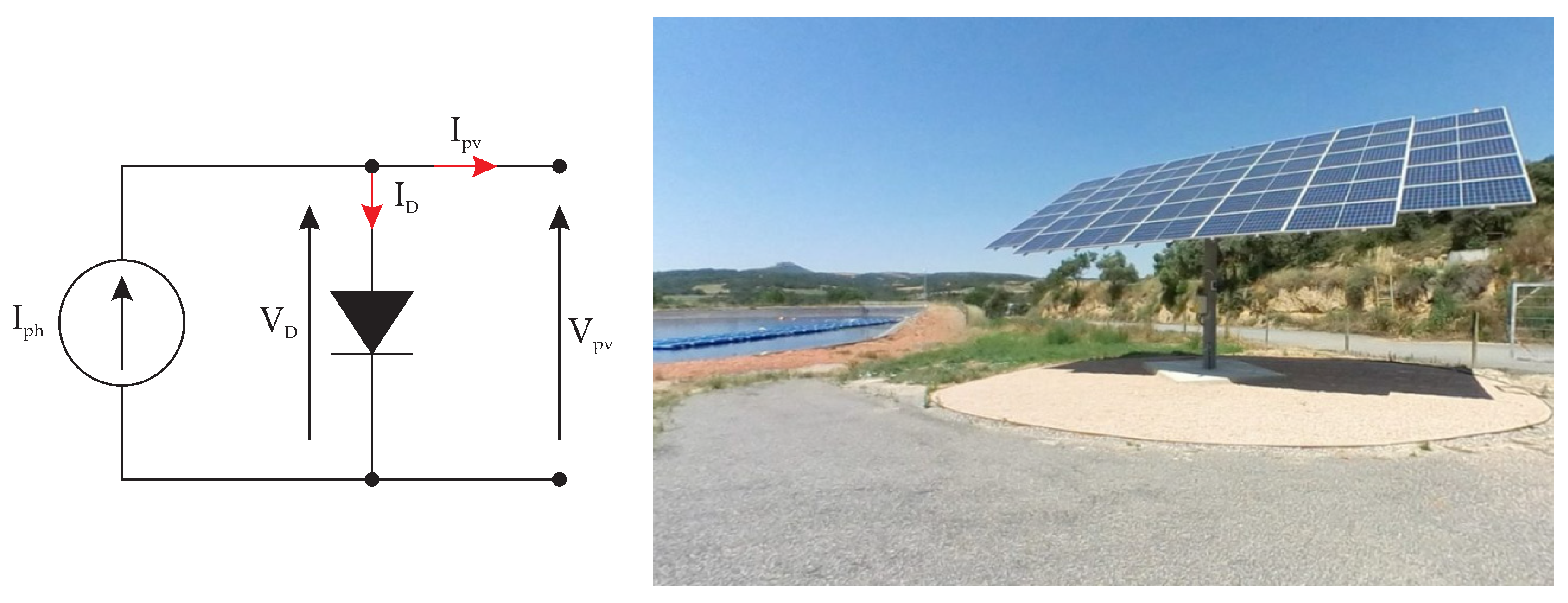
The electrical behavior of the PV-array is described by the single-diode model (
Figure 9), whose characteristic equation is given by the following:
Here, ipv is the photovoltaic output current; iSC is the short-circuit current; vPV is the array output voltage, which is regulated by the voltage on C1; vOC is the open-circuit voltage; RS is the series resistance; and vT is the thermal voltage of the PV cell. This nonlinear equation reflects the dependency of the PV output on both the environmental and electrical operating conditions. The single-diode PV model adopted here offers a reasonable trade-off between accuracy and computational efficiency for control development and simulation purposes. Although more complex models exist (e.g., double-diode or dynamic thermal–electrical coupling), they are often unnecessary for control-level design.
The sizing and dynamic behavior of the DC-link capacitor (C2) play crucial roles in maintaining voltage stability at the intermediate bus, especially under rapid load variations or switching transients. Adequate capacitor selection is essential not only to limit voltage ripple but also to ensure proper decoupling between the boost and inverter stages. An undersized DC-link may lead to degraded output quality or instability in the AC voltage waveform generated by the inverter.
The complete system was implemented and simulated using MATLAB-Simulink, allowing for time-domain analysis of the converter behavior, energy transfer, and control response. To evaluate the effectiveness of the partial-power architecture in conjunction with the PV source, dedicated control algorithms were developed. These are described in detail in the following section.
Furthermore, the proposed system architecture is inherently modular, allowing it to be extended to larger-scale PV arrays or integrated into distributed energy systems. Multiple converter units can be interconnected in series or parallel configurations, supporting increased power levels and enhancing redundancy. This modular approach aligns well with the scalability requirements of modern DC microgrids and smart-grid infrastructures.
3.1. Power Flow and Efficiency Analysis in Partial-Power Mode
In the studied
IPOS-based architecture, the PV array is connected in series with the output of the DC-DC converter. As a result, the total bus voltage is the sum of the PV output voltage and the converter output voltage, expressed as follows:
Under this topology, the converter does not need to process the entire power demand. Instead, the passive series path allows for part of the power to reach the load directly, which reduces the burden on the converter’s switching and magnetic components. Assuming ideal conditions, the voltage at the output of the converter (
vC2) can be expressed as a function of the PV voltage and the duty cycle (
D).
Substituting this into the expression, the instantaneous power processed by the converter is the following:
The instantaneous power generated by the photovoltaic array is given by the following:
While, the total power delivered to the load, assuming resistive emulation of the DC-bus current, can be written as follows:
The resulting power balance across the system can be expressed as follows:
Thus, the processed power ratio is the following:
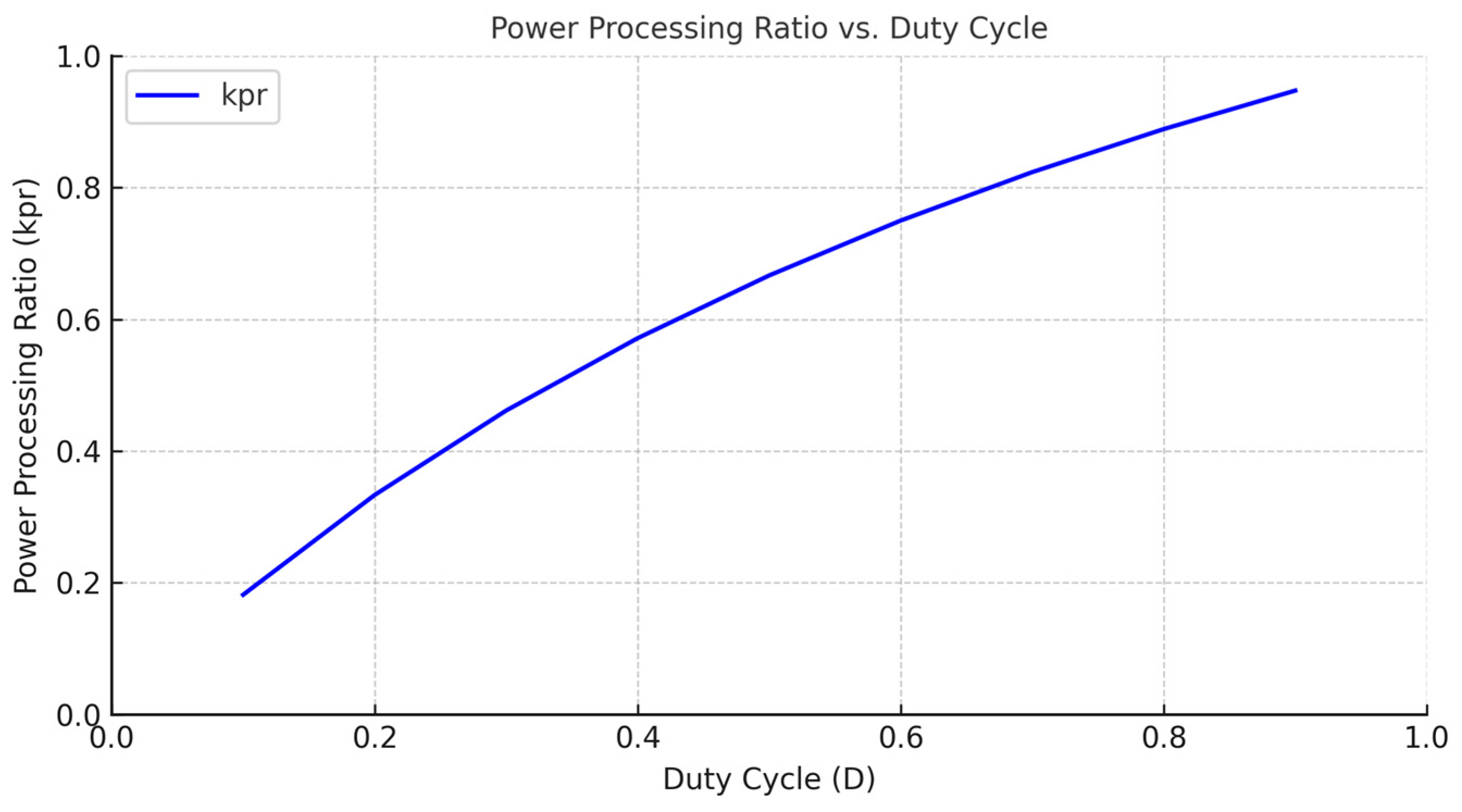
This expression highlights the dependency of kPR on the voltage gain and, indirectly, on the duty cycle (D). At low duty cycles, vC2 is small, and most of the power flows passively, maximizing the efficiency. Figure 11 illustrates how kPR evolves as a function of D, confirming that partial-power operation is most effective under low-to-moderate gain conditions.
To evaluate the energy performance, the system-wide efficiency (
ηsystem) is expressed as follows:
where
ηconv is the converter’s intrinsic efficiency, and
Pdirect is the direct power flow (total power that is not processed by the converter), that is, the power that flows directly from the source (PV) to the load. Analytical and simulated results (Figures 12 and 13) demonstrate that the overall efficiency increases as
kPR decreases, outperforming full-power architectures, especially in scenarios with low conversion demands. This methodological framework establishes a rigorous basis for analyzing and designing partial-power converters, linking topology, control, and energy flow characteristics. It also justifies the architecture’s suitability for photovoltaic systems, where efficiency and thermal optimization are critical.
This equation highlights the core principle of partial-power processing: the converter handles only a fraction of the total power, with the remainder directly transferred through the passive path. This configuration enables improved efficiency, lower thermal stress, and optimized component usage.
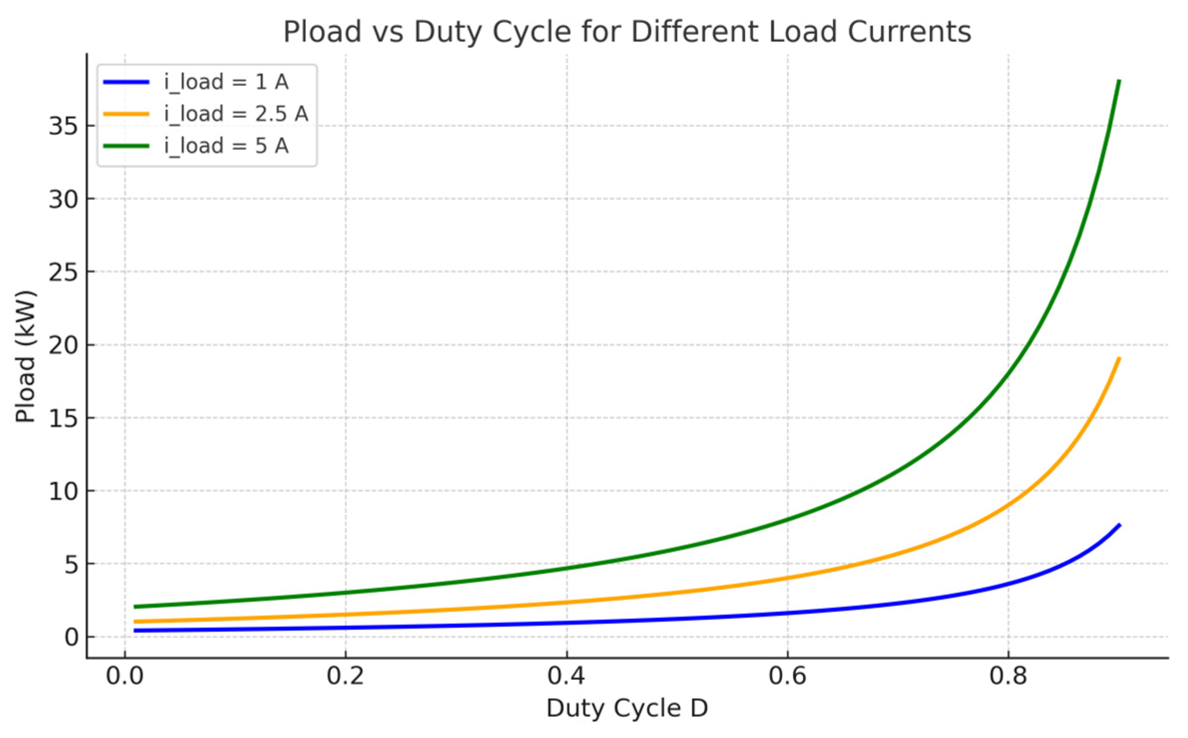
Figure 10 illustrates the evolution of the power delivered to the load (
Pload) as a function of the duty cycle (
D) for the following three representative values of load current: 1 A, 2.5 A, and 5 A. The results, obtained under ideal operating conditions and assuming a constant photovoltaic input voltage of +400 V, reveal the nonlinear dependence of the output power on the duty-cycle modulation. As analytically described in Equation (39),
Pload increases sharply as
D approaches unity—a trend that becomes more pronounced at higher load currents due to the combined rise in converter output voltage and total system power. The plotted curves emphasize the high sensitivity of the delivered power to small changes in the duty cycle, particularly in the upper operating range, highlighting the critical need for precise and stable duty-cycle control in partial-power converter architectures to ensure accurate power regulation and avoid overshoot or instability.
Figure 11 illustrates the relationship between the power processing ratio
kPR and the converter duty cycle (
D). In this architecture,
kPR depends solely on
D and remains independent of the load current, as both
Pconv and
Pload are linearly dependent on it. The graph highlights that, at low duty cycles, the converter processes only a small fraction of the total power, reducing conduction and switching losses. As
D increases,
kPR approaches unity, indicating that the converter begins to handle a greater share of the total power. This trend underscores the importance of optimizing the duty cycle to maintain high efficiency while minimizing converter stress.
It is worth noting that the system exhibits increasing sensitivity to control variations as the duty cycle (D) approaches unity. In this region, even small perturbations in D can produce significant changes in both the converter output voltage and the power processed. This behavior necessitates precise control resolution and stability in the duty-cycle modulation to maintain the desired performance and avoid overshoot or instability in dynamic operation.
3.2. Efficiency Analysis: Partial Power vs. Full Power
In partial-power converter architectures, the total power processed by the converter varies with the operating duty cycle (D). This behavior directly influences the overall system efficiency. As the duty cycle decreases, the voltage gain of the converter reduces, resulting in less power processed by the active conversion stage and more power flowing directly through the passive path. This section analyzes the relationship between system efficiency and duty cycle and compares it to the performance of a conventional full-power converter.
The estimated system efficiency for the partial-power converter can be expressed as follows:
where
ηconv is the efficiency of the converter, and
M is the system voltage gain defined as
vbus/
vpv. As
M increases with a higher
D, the denominator decreases, and
ηsystem becomes more sensitive to the internal efficiency. Conversely, at lower values of
D,
M approaches 1, and
ηsystem tends toward unity, maximizing the overall performance.
In contrast, a full-power converter processes the entire load power regardless of
D, so the overall system efficiency equals the internal converter efficiency, as follows:
This distinction underscores one of the principal advantages of partial-power converter architectures: by actively processing only a fraction of the total system power, they can achieve superior global efficiency compared to conventional full-power configurations. When appropriately designed and controlled, the reduced processing burden leads to lower conduction and switching losses within the active stage.
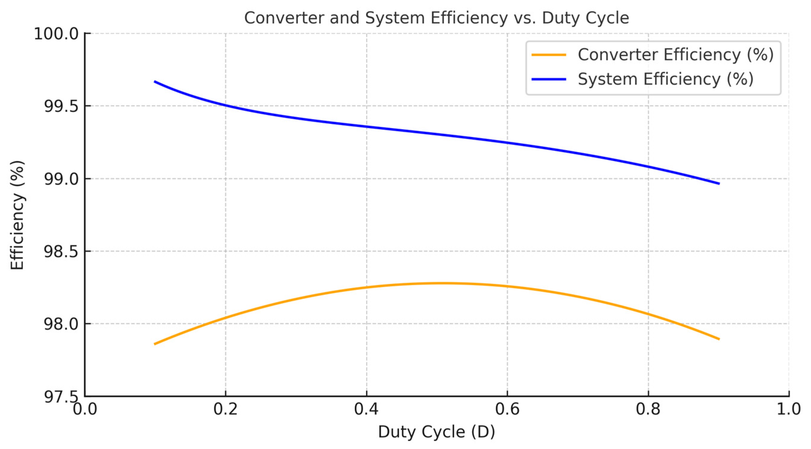
Figure 12 presents a comparative analysis of system efficiency as a function of the duty cycle (
D), assuming an internal converter efficiency (
ηconv) of approx. 98.25%. The results clearly show that the partial-power configuration outperforms the full-power counterpart, particularly in the low-to-moderate duty-cycle range, where the converter handles a smaller portion of the total energy flow. This operational regime maximizes the benefit of partial-power processing by allowing for more energy to be transferred through the passive path, thus minimizing losses and enhancing overall performance.
In this study, a more realistic efficiency model for the converter has been adopted, incorporating the degradation observed under light-load conditions. Specifically, a slight efficiency penalty is introduced at low power levels due to the relative impact of fixed losses—including core, switching, and control circuitry losses—which become dominant when the processed power decreases. This phenomenon, commonly observed in converter architectures operating at low duty cycles, leads to a gradual reduction in efficiency as the duty cycle moves toward the lower end of the operational range. Accordingly, the converter efficiency can be approximated by the following expression:
where
ηnominal denotes the peak or nominal efficiency under full-load operation (typically around 98.25%), and Δ
η(
D) represents a nonlinear decreasing function that quantifies the efficiency loss associated with reduced power processing. This model provides a more accurate representation of the converter’s performance over a wide operating range and is essential for correctly estimating the global system efficiency in partial-power architectures.
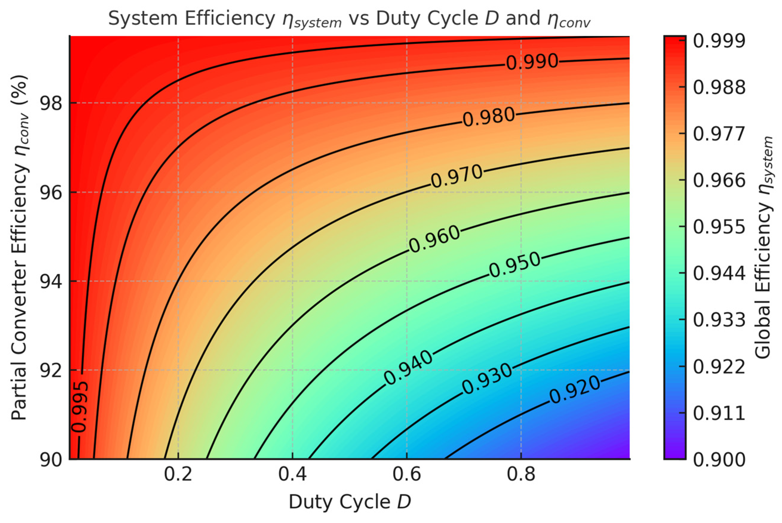
Figure 13 illustrates a contour map of the global system efficiency (
ηsystem) as a function of the duty cycle (
D) and the internal efficiency of the partial-power converter (
ηconv). The map reveals the interaction between the control modulation and converter performance, highlighting how system-level efficiency improves when the processed power fraction is minimized, i.e., at lower values of duty cycle (
D). This is because, under these conditions, the active converter handles only a small portion of the total load power, while the majority is transferred directly via the passive path, thereby avoiding conversion losses.
At high values of ηconv (above 97%) and low-to-moderate values of D (below 0.4), the global efficiency reaches or exceeds 99%, which is significantly higher than what would be achievable with full-power processing using the same conversion stage. Conversely, when D→1, the system becomes increasingly dependent on the converter, and ηsystem asymptotically approaches ηconv, as the passive contribution diminishes. The iso-efficiency contours (from 92% to 99.5%) provide insight into optimal design regions for partial-power architectures, and serve as a useful tool for evaluating the trade-offs between converter quality and control requirements in high-efficiency renewable energy systems.
The results presented in this section emphasize the critical role of the converter architecture in optimizing system-wide energy performance. The iso-efficiency contours guide the selection of duty cycle and converter efficiency pairs to meet specific performance targets. To fully exploit the advantages of partial-power processing, it is essential to implement robust and efficient control algorithms, which are addressed in the following section.
5. Results
The proposed PV partial-power converter system has been modeled and simulated using
MATLAB-Simulink. The values of the main electrical and control parameters are summarized in
Table 5 (refer to Nomenclature section for details).
The maximum power handled by the partial-power converter (
Pppmax) is directly determined by the total photovoltaic generation capacity connected to its input stage. This total input power can be expressed as follows:
where
Ns represents the number of PV modules connected in series per string,
Np denotes the number of parallel strings, and
Ppv is the rated power of each individual panel. This formulation provides a direct estimation of the upper power limit that the converter must be capable of processing under full irradiance and optimal operating conditions, and its serves as a key design criterion for sizing the active components and the thermal management system of the converter stage.
All simulations were carried out using MATLAB-Simulink with a fixed-step solver and a sampling time of 5 μs, ensuring accurate representation of switching dynamics. Standard test conditions were assumed for the PV array, as follows: irradiance of 1000 W/m2 and ambient temperature of 25 °C. The electrical parameters of the modules and passive components were selected based on commercially available hardware, allowing for straightforward extrapolation to real-world implementation scenarios. These settings establish a realistic framework for evaluating the dynamic performance and energy efficiency of the proposed system under typical operating conditions.
5.1. Simulation Analysis
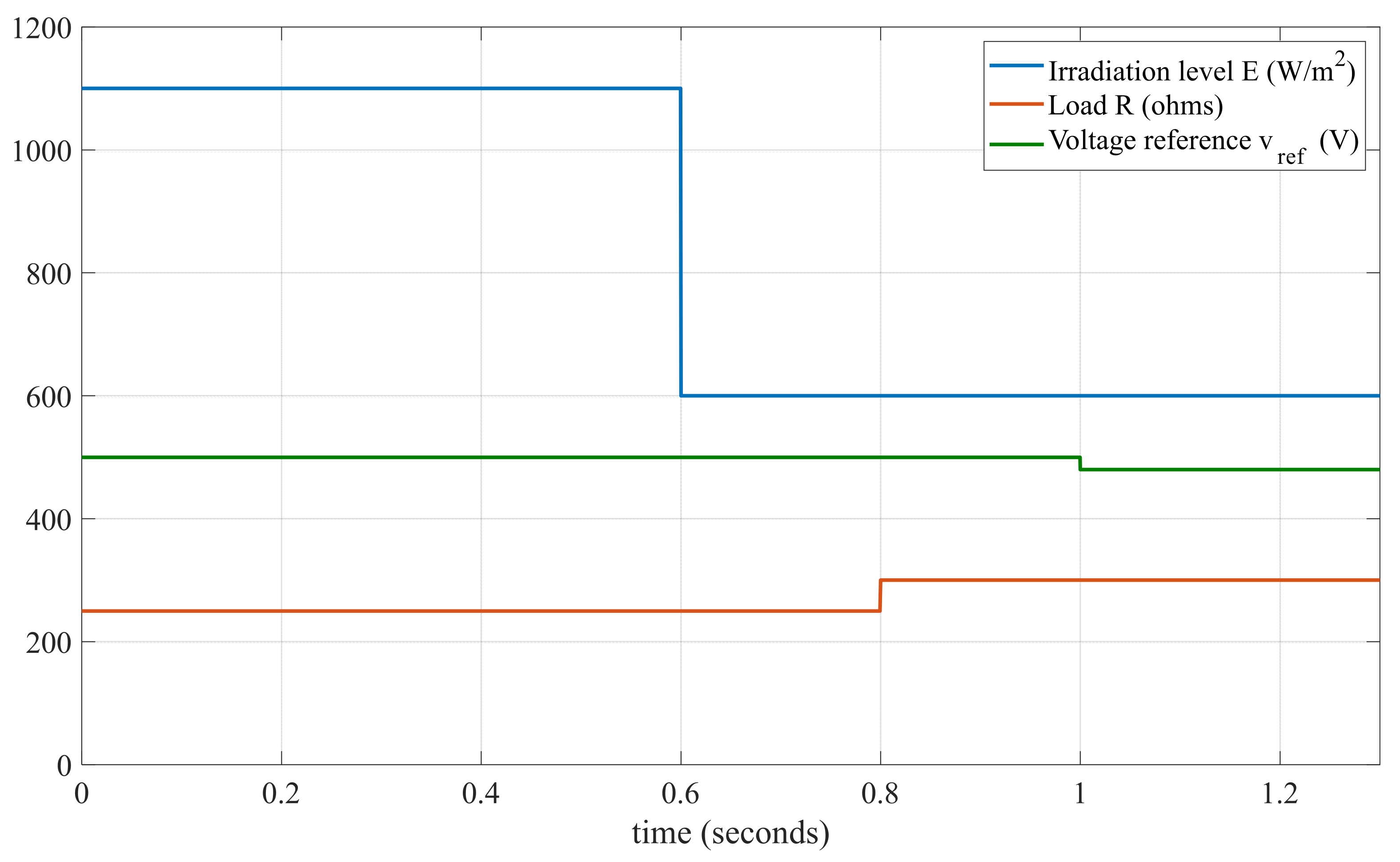
Figure 15 illustrates the temporal evolution of the test conditions applied to the photovoltaic system under real-time validation. The upper plot shows the step changes in the following three critical parameters: solar irradiance
E (in W/m
2), load resistance
R (in ohms), and reference voltage
vref (in volts). These variations are introduced to emulate realistic operating scenarios, including transient solar conditions and load disturbances, which pose a challenge for voltage regulation and dynamic stability. The system is initially subjected to high irradiance (1100 W/m
2) and a moderate load, followed by a sudden drop in solar input to 600 W/m
2. Later, both the load and the voltage reference are varied independently to evaluate the controller’s response under multiple perturbations. The dynamic nature of these changes directly affects the power available from the PV generator and the current demanded by the load, making it a representative testbench for converter performance assessment.
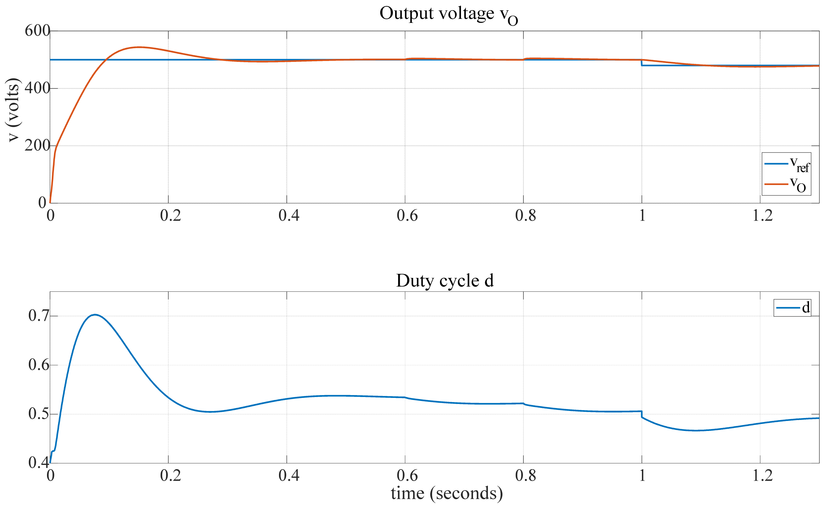
Despite these variations, the system maintains regulated output behavior, as shown in
Figure 16, thanks to the robustness of the proposed partial-power topology and its dual-loop PI–SMC control scheme. The output voltage (
vO) (DC-bus) closely follows the reference (
vref) with minimal steady-state error and low ripple, while the duty cycle (
D) adapts smoothly to the imposed transitions. This confirms the converter’s ability to handle time-varying conditions while preserving output stability and efficiency.
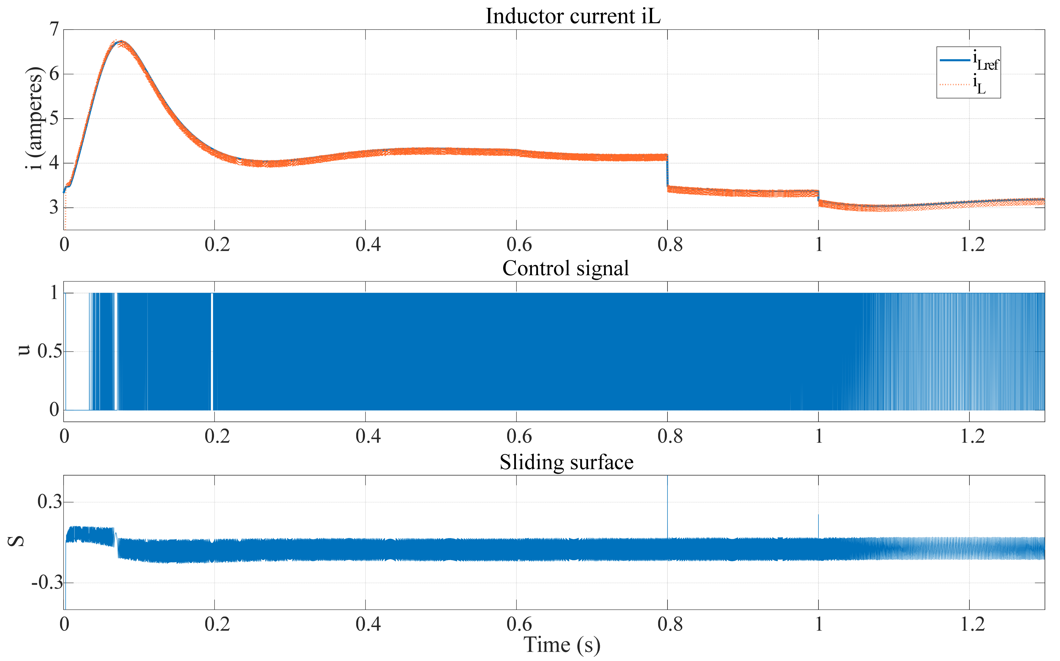
Figure 17 illustrates the internal dynamics of the current control loop governed by the Sliding-Mode Controller (
SMC). The waveform of the inductor current (
iL) shows fast convergence toward its reference value (
iLref), with minimal steady-state error and strong disturbance rejection. The sliding surface signal (
s(
t)
= iL −
iLref) demonstrates that the system rapidly reaches and maintains sliding mode operation, confirming the existence of a sliding regime. The control action (
u(
t)) exhibits characteristic high-frequency switching, inherent to the discontinuous nature of the
SMC law. This confirms that the controller enforces the intended dynamics by switching the control state in response to deviations from the sliding surface, ensuring robust and stable current regulation.
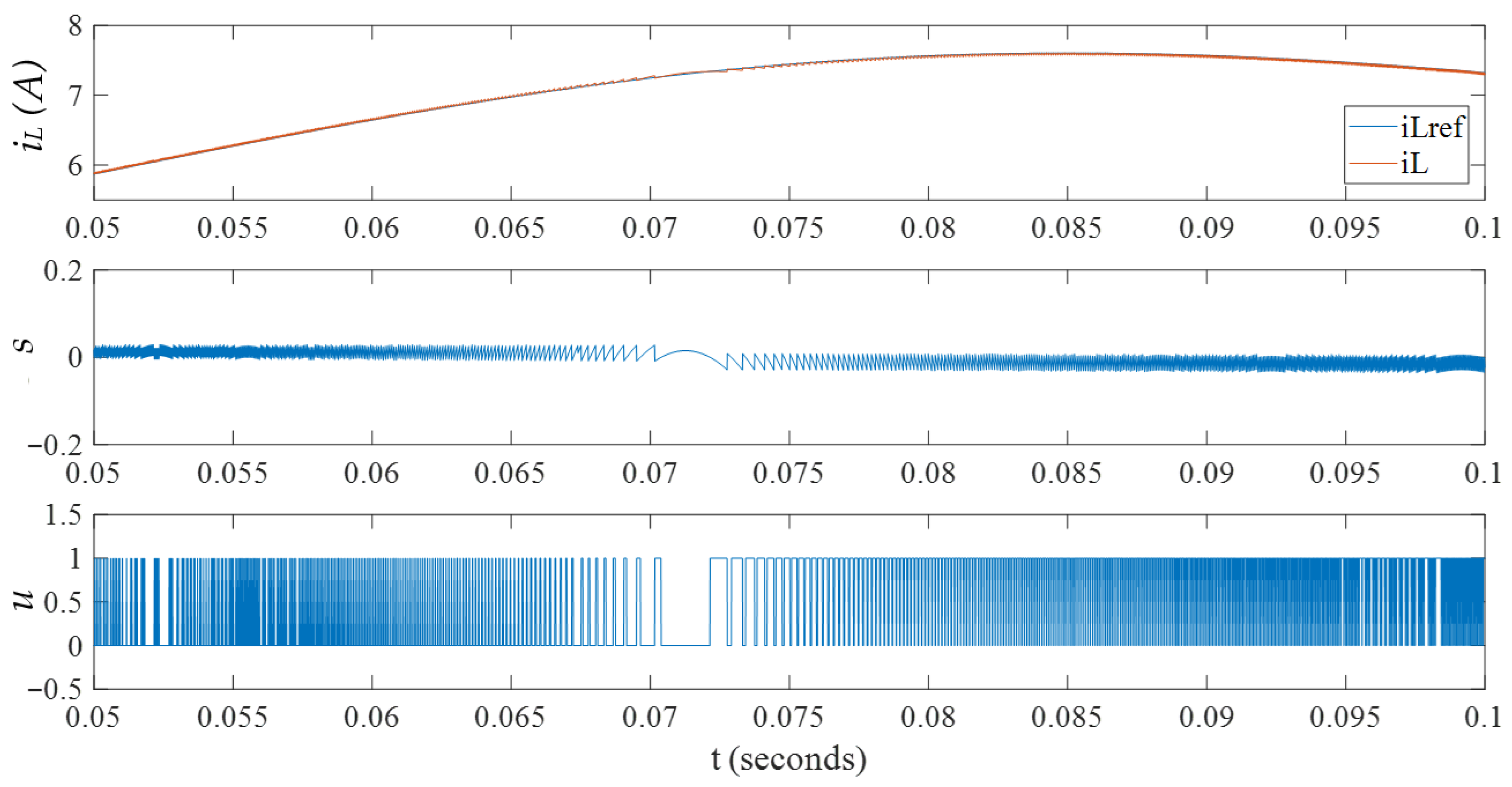
Figure 18 provides a detailed view of the switching behavior associated with the sliding mode control implementation. The control signal alternates between two discrete states (
u = 0 and
u = 1), forcing the system’s trajectory to remain within the vicinity of the sliding surface. This high-frequency switching is a direct consequence of the discontinuous control law, which aims to counteract disturbances and model uncertainties by reacting instantaneously to sign changes in the error. Although this behavior ensures robustness and precision, it also reveals the presence of chattering—a known limitation of ideal SMC—which may require mitigation techniques such as hysteresis bands or boundary layer approximations in practical implementations.
The simulation results confirm that the combined PI–SMC control structure achieves fast, stable, and robust regulation of both current and voltage, even under dynamic operating conditions. To further validate its performance under real-time constraints, the system was subsequently implemented in a hardware-in-the-loop environment using OPAL-RT.
5.2. Real-Time Simulation with OPAL-RT
The proposed system model has been implemented within a real-time simulation environment using the OPAL-RT platform. This Hardware-in-the-Loop (HIL) configuration enables the evaluation of the converter’s dynamic behavior and control performance under realistic operating conditions, leveraging FPGA-based execution. The use of HIL has been widely adopted in power electronics research and is considered a robust validation methodology when direct prototyping is impractical due to voltage, power, or cost constraints.
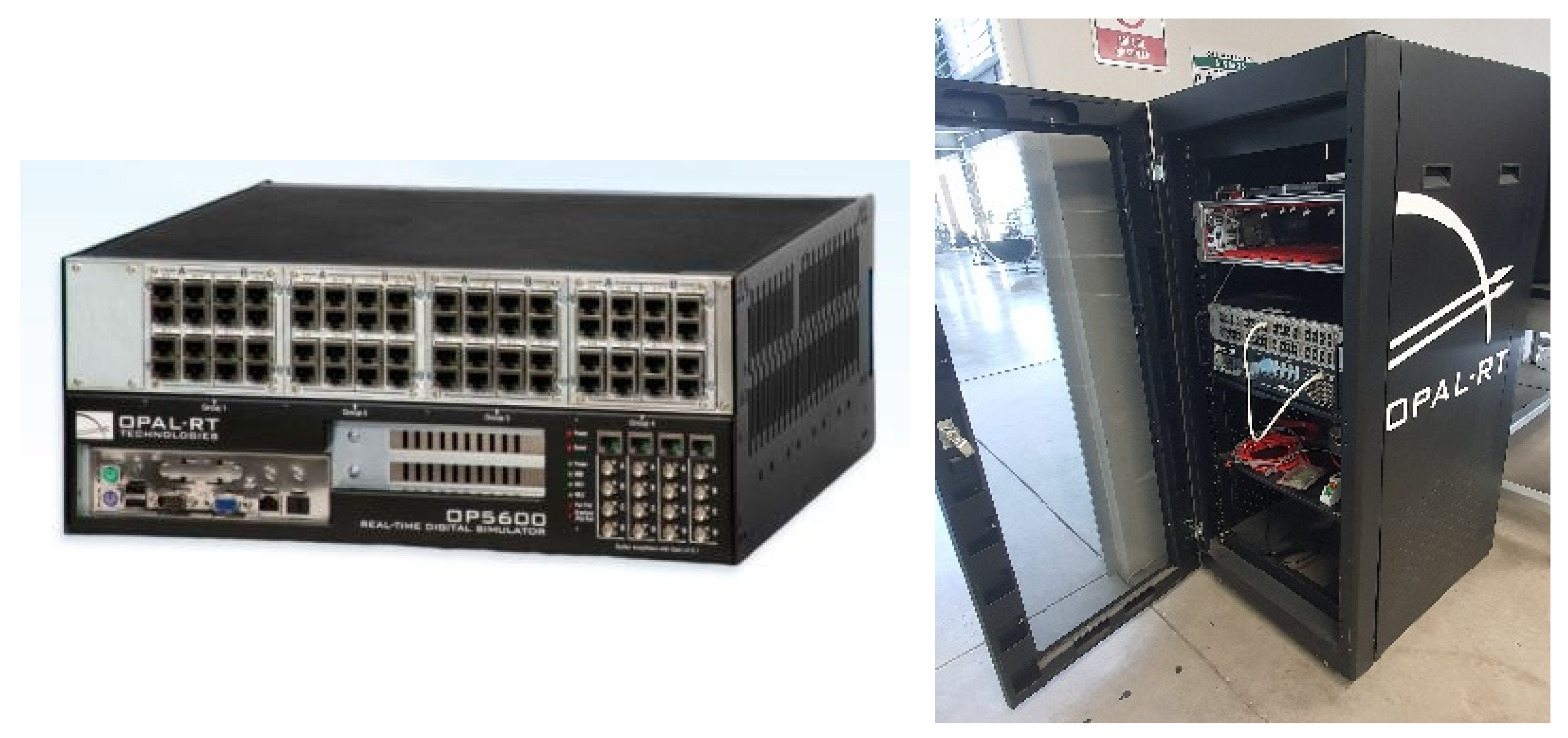
Figure 19 shows the real-time simulation platform based on
OPAL-RT technology, used for
hardware-in-the-loop (
HIL) validation of the proposed partial-power converter system. The
OPAL-RT HIL environment enables high-fidelity emulation of power electronic systems with sub-microsecond time resolution, allowing for the execution of real-time models that interact dynamically with physical controllers. This setup provides a safe, reproducible, and flexible framework to assess control strategies and converter behavior under realistic operating conditions without the risks or limitations associated with full-scale laboratory hardware testing. The
HIL methodology plays a crucial role in bridging the gap between numerical simulation and experimental prototyping, supporting accelerated development and robust validation of advanced control schemes.
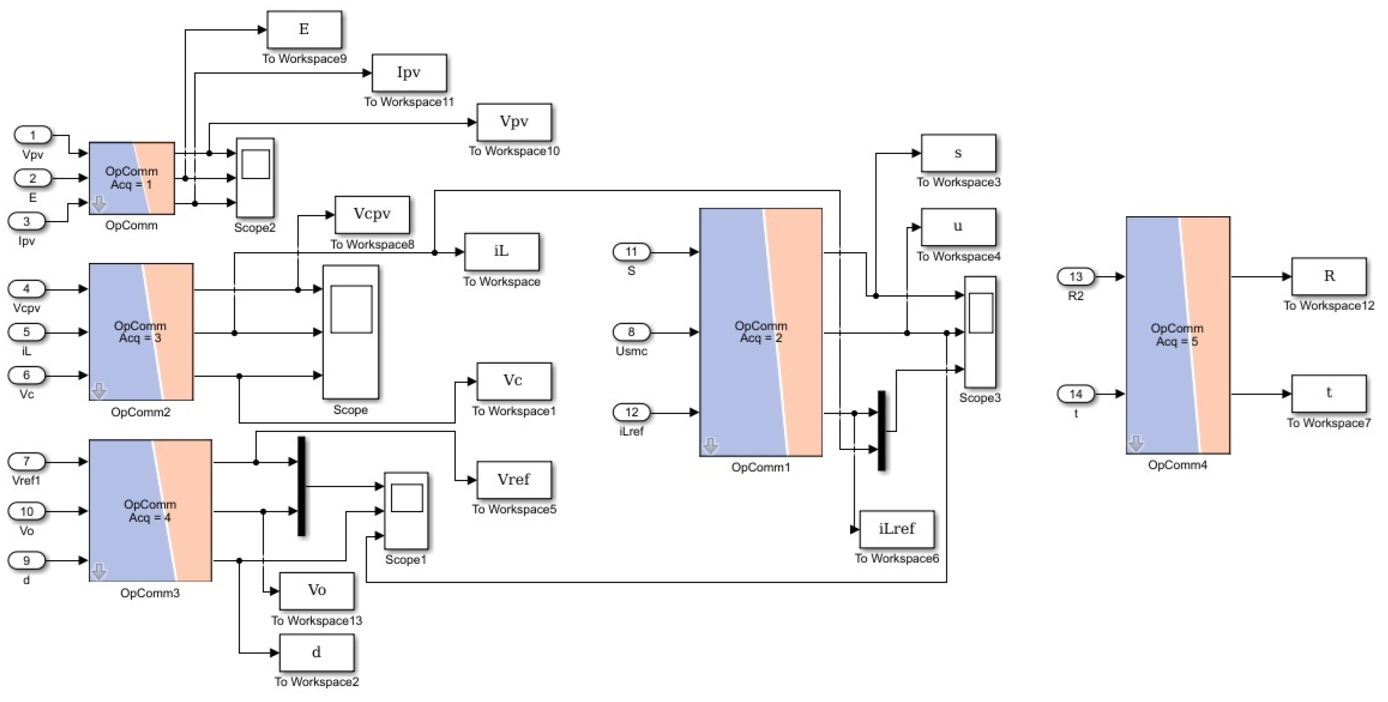
Figure 20 presents the high-level block diagram of the simulation model implemented in the
OPAL-RT environment, detailing the signal acquisition, communication, and visualization structure used for real-time execution. The model includes multiple
OpComm and
OpComm Acq modules responsible for bidirectional data exchange between the physical controller and the digital real-time model. Each key system variable—such as input/output voltages, inductor currents, duty cycle, and control references—is monitored and logged through interface blocks, enabling comprehensive analysis of the system response under dynamic operating conditions. This modular and synchronized configuration ensures real-time observability and interaction with the converter model, as well as supports hardware-in-the-loop experimentation with high fidelity and temporal resolution.
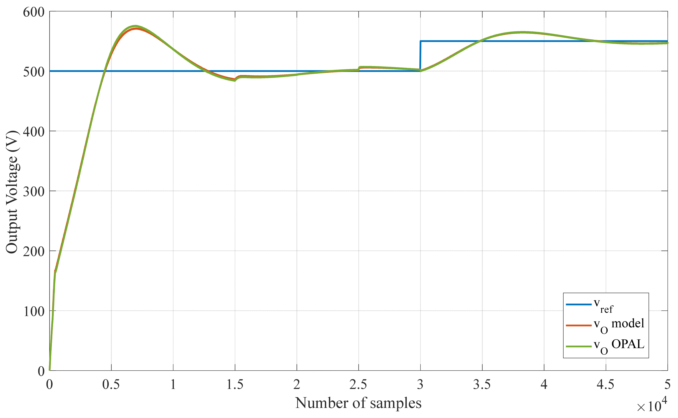
Figure 21 compares the output voltage dynamics obtained from the
MATLAB-Simulink simulation and the real-time execution on the
OPAL-RT platform. The results show excellent agreement between both environments, with the voltage signal exhibiting smooth transient response and accurate tracking of the reference in both cases. Minor differences in the rise time or steady-state ripple may be attributed to numerical discretization and the real-time scheduling constraints of the hardware-in-the-loop system.
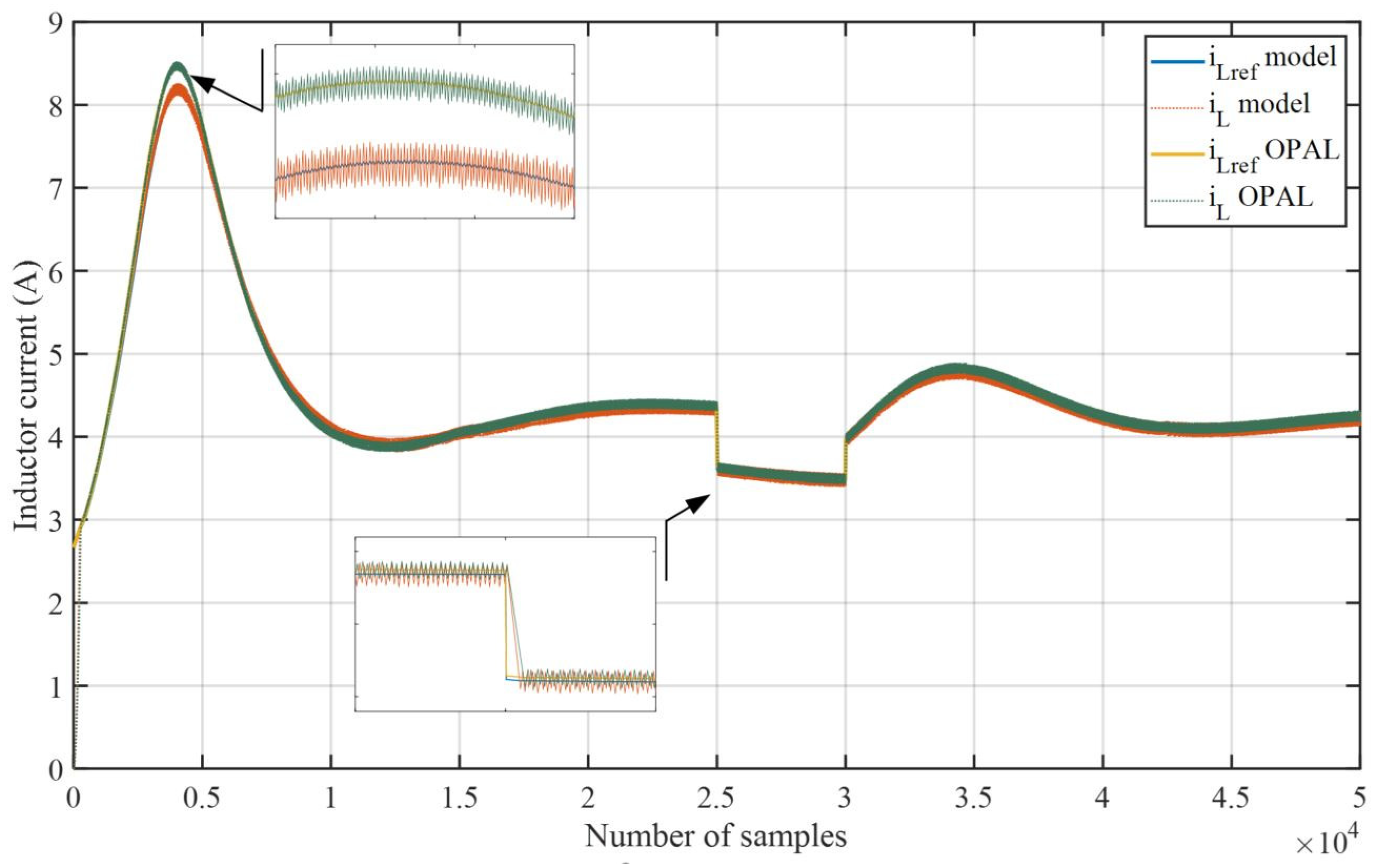
Figure 22 presents the evolution (detail) of the inductor current as simulated in
MATLAB-Simulink and replicated in
OPAL-RT. The current follows the expected trajectory in both cases, confirming that the sliding mode current controller maintains stable operation and correct switching behavior when deployed on
FPGA-based hardware. The high similarity between both responses validates the effectiveness of the proposed control algorithm and its feasibility for embedded real-time applications. The observed response time in both the simulated and HIL results suggests an effective bandwidth exceeding 3 kHz, consistent with typical design expectations for fast current-mode regulation in power converters.
After compiling the system for
FPGA execution, the model was simulated with a fixed step size of 20 µs using a
Runge-Kutta solver.
Figure 21 and
Figure 22 compare the dynamic response of the
MATLAB-Simulink model and the
OPAL-RT hardware implementation for the output voltage and inductor current, respectively. The results confirm excellent agreement between both platforms, with accurate tracking of the reference signals in both cases. Given the converter’s voltage and power rating, full-scale hardware testing poses significant practical challenges. These include safety risks, the need for isolation and protection hardware, and access to high-voltage laboratory infrastructure. In this context, real-time
HIL simulation offers a technically robust and economically viable alternative. It enables closed-loop validation under realistic dynamic conditions, ensuring that both control algorithms and system behavior are accurately characterized without the limitations of physical prototyping at early development stages.
Beyond validating the steady-state and dynamic performance of the control system, the real-time HIL experiments also confirm the robustness of the converter’s response to parameter variations and external disturbances. The ability to inject controlled transients, emulate load fluctuations, and modify environmental conditions (e.g., irradiance profiles) in a fully deterministic and repeatable manner is a key advantage of the HIL framework. Furthermore, the results obtained from the OPAL-RT platform closely match the expected theoretical behavior predicted by the analytical model, thereby reinforcing the consistency between the system-level design, control strategy, and hardware implementation. This level of correlation substantiates the applicability of the proposed architecture to practical photovoltaic systems with high reliability and minimal design uncertainty.
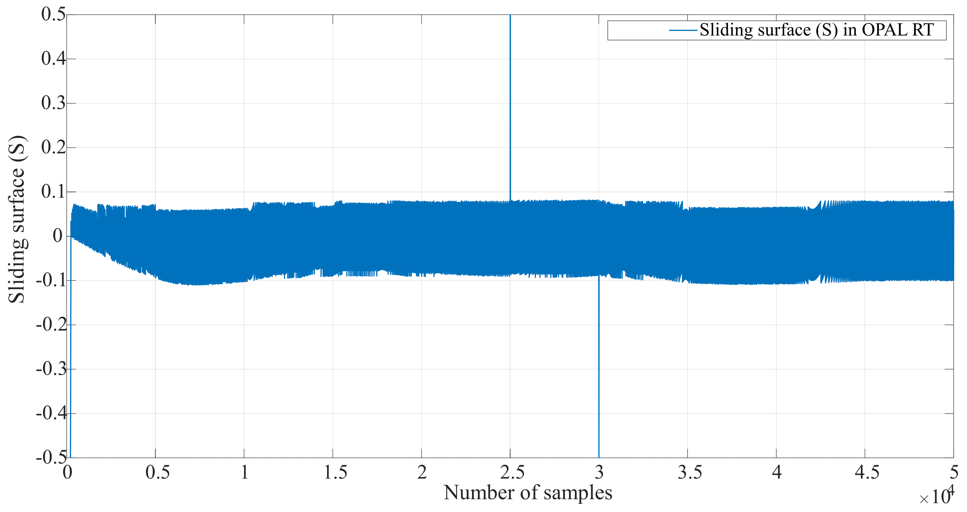
Finally,
Figure 23 shows the sliding surface obtained in the real-time implementation, verifying the correct operation of the sliding mode control in the
FPGA-based environment.
The simulation and real-time results demonstrate the accuracy, robustness, and hardware feasibility of the proposed control architecture, confirming its suitability for partial-power converter applications in dynamic environments. The following section summarizes the main findings and outlines the conclusions of this study.
5.3. Comparative Analysis with Recent Works
To evaluate the relevance and competitiveness of the proposed partial-power converter system, a comparative analysis is conducted against recent contributions in converter architectures based on partial-power processing (PPP). The goal is to assess the proposed design in terms of efficiency, control robustness, implementation feasibility, and suitability for PV systems.
Table 6 provides a structured overview of relevant works published in the last few years, highlighting key parameters, such as converter topology, energy efficiency, estimated processed power ratio (
kPR), conversion characteristics, isolation, application domain, and primary innovations. The concept of Partial-Power Processing (PPP) has gained substantial attention due to its potential to increase global system efficiency by reducing the portion of energy processed through active converter stages. Unlike full-power converters, which handle the entire power flow, PPP architectures operate by interconnecting the load in series or parallel with the energy source, thus allowing part of the power to bypass the converter via a passive path. This design strategy enables notable reductions in conduction losses, magnetic component sizing, and thermal stress, which are especially beneficial in high-efficiency, space-constrained, or cost-sensitive applications.
As shown in
Table 6, a wide range of converter topologies have been explored within the PPP framework, including both isolated (e.g., PSFB, DAB, and bidirectional transformer-based stages) and non-isolated implementations (e.g., buck-boost and Ćuk). Reported efficiencies often exceed 98%, with some systems achieving up to 99.5% under optimized conditions. However, such figures must be interpreted considering the corresponding power processing ratio (
kPR), which typically ranges from 0.2 to 0.5 in most cases. This parameter directly indicates the fraction of total power processed by the converter, with lower values implying improved energy utilization through the direct path.
Another relevant factor is the type of voltage conversion performed by the architecture. Most isolated designs support bidirectional or step-up/down conversion, providing flexibility for applications such as electric vehicle charging, electrolysis systems, or battery interfacing. Non-isolated topologies, while generally simpler, are typically constrained to unidirectional operation, but still offer sufficient performance for photovoltaic (PV) or industrial auxiliary applications.
In comparison to the reviewed architectures, the proposed system distinguishes itself by combining several advantageous features, as follows:
It uses a non-isolated buck-boost IPOS configuration, which simplifies the design while maintaining step-up capability for PV integration;
It achieves an estimated system efficiency of 98.25%, validated through both simulation and real-time Hardware-in-the-Loop (HIL) implementation on the OPAL-RT platform;
The converter operates with a processed power ratio kPR ≈ 0.18–0.4, depending on duty cycle and load, thereby minimizing active-stage stress;
A dual-loop control strategy combining Proportional–Integral (PI) voltage regulation and Sliding Mode Current Control (SMC) is implemented, offering robust performance under dynamic conditions and enhancing MPPT compatibility;
Given that kPR ≈ 0.2–0.4, the power stage components can be sized to handle only 20–40% of the total power, resulting in a proportional reduction in magnetic volume and switch rating.
In summary, while many works in the literature demonstrate high efficiency or advanced topological features, few combine those aspects with real-time validation and a scalable, low-complexity control approach. The proposed converter, therefore, contributes a practical and experimentally supported alternative for distributed PV systems and DC microgrids, bridging the gap between theoretical efficiency and real-world applicability.
In contrast to intelligent or adaptive control schemes requiring extensive computation or parameter tuning, the PI–SMC implementation offers a low-complexity yet high-performance alternative compatible with real-time embedded systems.
Despite the demonstrated advantages of the proposed architecture, several design limitations must be acknowledged. First, the control system exhibits increased sensitivity as the duty cycle approaches unity, where small perturbations in modulation may lead to large variations in output voltage and power transfer, thus requiring high-resolution control and robust stability margins. Second, the inherent structure of the IPOS configuration imposes constraints on the achievable voltage gain, particularly in applications requiring wide dynamic range or deep step-up conversion. Finally, while Sliding Mode Control (SMC) provides excellent robustness, it may introduce high-frequency chattering in the control signal, which can lead to increased switching losses or Electromagnetic Interference (EMI). This issue can be mitigated through the incorporation of boundary layer approximations or hysteresis modulation strategies. These trade-offs should be carefully considered in practical implementations and guide future refinements in both topology and control design.
