1. Introduction
To achieve high performance and effective power reduction, radio frequency (RF) receivers for communication systems often require analog-to-digital converters (ADCs) with a high dynamic range (DR) and high energy efficiency. The signal power received by antennas can vary significantly due to different operating environments and transmission distances, necessitating high sensitivity in receivers to ensure signal accuracy. Among the various ADC architectures, delta-sigma (DS) ADCs have become a popular choice for communication systems, since they provide high resolution with high energy efficiency.
Successive approximation register (SAR) ADCs are famous for their high energy efficiency, but their resolution is typically limited to about 10–12 bits unless extensive calibration and trimming are applied [
1]. DS ADCs can achieve higher resolution with oversampling and noise shaping. However, high-order DS modulators (DSMs) and multi-bit DSMs, typically employed to achieve high dynamic range (DR), are not energy-efficient. This is due to the use of higher oversampling ratio and multiple integrators in a single-bit high-order DSM or a power-hungry flash quantizer in a multi-bit DSM [
2]. Therefore, reducing power consumption in ADCs is critical, particularly for automotive-grade applications.
Discrete-time delta-sigma (DT-DS) modulators, while capable of high performance, are limited in terms of sampling frequency because of the stringent requirements on fast, high-precision sample-and-hold (S/H) building blocks [
3,
4,
5]. In contrast, continuous-time delta-sigma (CT-DS) modulators offer advantages such as low power consumption, inherent anti-aliasing performance, simplified input drive requirement, and relaxed bandwidth requirements [
6,
7,
8]. Some recently proposed DT-DS modulators with finite impulse response (FIR) digital-to-analog converters (DACs) could satisfy the requirements of portable and biomedical applications constrained by battery life [
9,
10]. A FIR DAC reduces the signal swing of the loop filter, further relaxing linearity requirements. However, it alters the loop dynamics, requiring an additional compensation path to maintain stability. CIFF (Cascade of Integrators FeedForward) topologies [
9] intrinsically minimize integrator output swings, enhancing linearity and relaxing slew-rate demands. CIFB (Cascade of Integrators Feedback) structures [
10] offer superior stability and quantization noise shaping. The Cascade of Integrators FeedForward and Feedback (CIFF-B) topology combines feedforward and feedback paths to suppress out-of-band noise while minimizing integrator output swing.
Integrator topology in the loop filter critically impacts power efficiency, linearity, and dynamic range. The hybrid RC-GMC integrator topology uses the RC integrator under large swings in the critical first stage and GMC integrators in subsequent stages for the advantage of speed, area, and power. GMC integrators offer high speed and area efficiency, while their inherent nonlinearity poses challenges in high-precision applications. Conversely, RC integrators provide superior linearity but they are limited to bandwidth and higher power consumption for equivalent settling. A hybrid integrator topology employs an RC integrator in the first stage followed by GMC stages to strategically balance these trade-offs. The first integrator directly processes the widest dynamic range signal within the loop filter. This stage requires the highest linearity to accurately represent the input signal without introducing significant distortion (THD) or noise modulation, which would directly degrade overall ADC performance. Due to the large dynamic range of the first stage, an RC integrator is used to ensure linearity, while the dynamic range after the first stage decreases. Smaller swings mitigate GMC’s inherent nonlinearity. GMC integrators reduce power consumption and die area compared to RC equivalents.
Multi-bit quantizers reduce in-band quantization noise improve linearity, but they require dynamic element matching (DEM) [
11]. This further increases the power dissipation and design complexity of the quantizer [
12]. Considering the bandwidth’s requirement, the proposed CT-DS modulator employs a third-order CIFF-B architecture with a 1-bit quantizer optimized for sub-1 GHz receivers, balancing resolution and energy efficiency.
This paper presents the design method and circuit implementation of a CT-DSM. Based on the system requirements, the modulator was designed, modeled and coefficient-scaled using MATLAB Simulink (version number: 24.1.0.2537033) tools. Non-idealities of operational amplifiers (op-amps) and clock signals were systematically modeled to determine key circuit design parameters and guide the practical implementation.
The prototype achieves a 76.1 dB peak signal-to-noise (SNR) and a Schreier figure of merit (FoM) of 160.7 dB based on signal-to-noise and distortion ratio (SNDR) in a 500 kHz bandwidth, while consuming only 0.8 mA from a 1.8 V supply in a 180 nm CMOS process.
This paper is organized as follows:
Section 2 analyzes the system architecture and CIFF-B loop filter design. In
Section 3, the circuit architecture implemented in this paper is illustrated.
Section 4 shows the measurement results of the circuit. Finally, the conclusions are presented in
Section 5. 2. Architecture
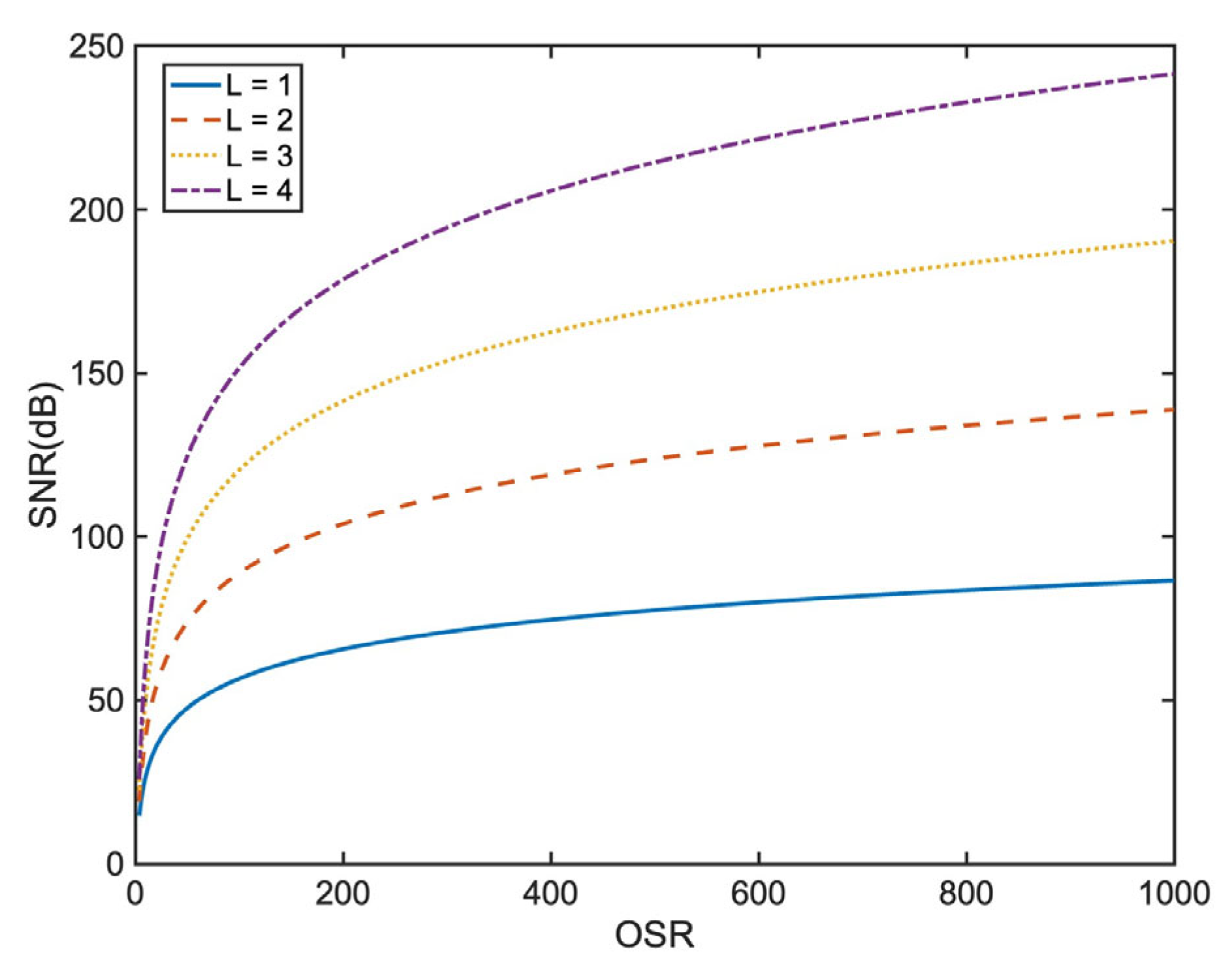
The operating voltage of the ADC in this design is 1.8 V, and in order to achieve a 14-bit resolution, the SNR needs to be above 86 dB. For an ideal modulator without jitter and nonlinearity, the relationship between the SNR, the order and the oversampling rate (OSR) is given by
where
L is the order of the modulator. According to the mathematical formulas,
Figure 1 illustrates the ideal curves without non-ideal factors in circuits. High-order modulators can improve system accuracy, but their stability and the input dynamic range will be limited. In addition, higher-order modulators require more integrators, which significantly increase the power consumption. High-OSR approaches are sensitive to clock jitter. This design chooses a third-order CIFF-B loop filter with a 150 OSR to achieve a 86 dB SNR.
The receiver path consists of a low-noise amplifier (LNA), a mixer, an inter-mediate frequency (IF) amplifier, an ADC, and an RX digital signal processor (RX DSP), as shown in
Figure 2. This chain is controlled by configurable RF front-end registers. Programmable LNA input is provided to obtain optimum performance matching for each frequency range and to allow multi-band applications. The subsequent double-quadrature mixer converts the received RF signal into a low inter-mediate frequency, while achieving high image rejection through the precise phase and amplitude matching of its quadrature paths. An IF amplifier provides additional gain and improves the receiver sensitivity. The ADC converts the IF signal into the digital domain with a resolution tailored to the system’s dynamic range requirements, through a clock coming from the PLL. The RX DSP performs channel filtering and converts the digital output signal of the ADC into the baseband for demodulation. Due to the digital realization of these functions, the RX DSP can be adapted to the needs of many different applications.
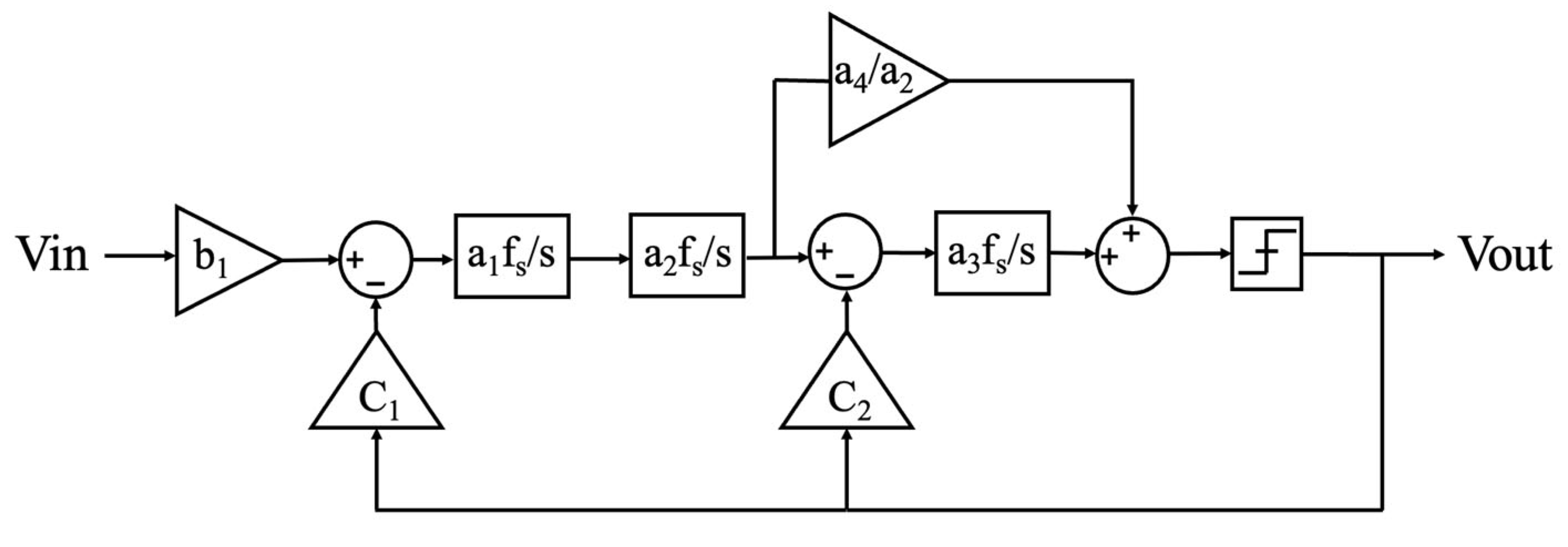
Figure 3 features a block diagram of the CT-DS modulator. This system employs a third-order CIFF-B topology, operating at a sampling frequency of 150 MHz. This architecture synergizes the advantages of CIFF and CIFB structures.
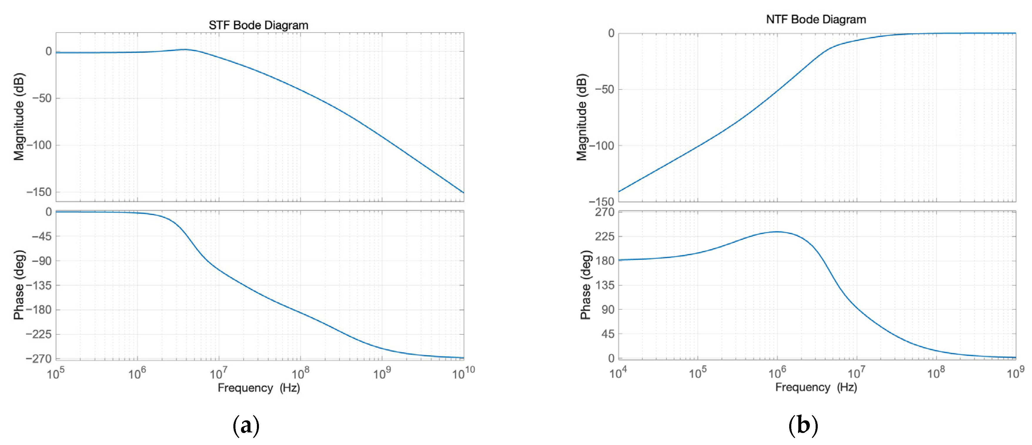
The loop filter coefficients are derived via Simulink behavioral modeling, where Laplace-domain transfer functions are optimized for stability and in-band noise shaping. A 1-bit quantizer is selected to eliminate nonlinearity concerns, with its output range constrained to prevent overloading downstream stages. The Bode plots in
Figure 4 show that the noise transfer function (NTF) has a high-pass shape, and the signal transfer function (STF) has a low-pass characteristic. The in-band STF gain is very close to 0 dB with no peaking, which is critical for stability.
To implement the CIFF-B loop filter structure, coefficient a
4/a
2 in
Figure 3 can be replaced by the feedforward GmC integrator, which has an equivalent gain of a
4 and operates in parallel with the other two GmC integrators. The quantizer is modeled using a relay block with an output range of −1 to 1. The current value of the current-steering DAC (IDAC) feedback is represented by a gain module, which is converted into a voltage value by multiplying its resistance, allowing it to be calculated with other voltage variables. An S/H block is used to simulate the process of clock sampling. With the usage of Simulink and MATLAB, the appropriate transfer function and the coefficient of each stage are determined, providing guidance for circuit design. To reduce the noise effects, the output noise of each module is extracted from circuit simulation and sent to MATLAB to calculate its contribution. The CIFF-B topology’s inherent robustness to process variations further ensures yield across corners, making it suitable for mass production in 180 nm CMOS. Special attention should be paid to modules with significant noise contribution for further optimization.
3. Circuit Implementation
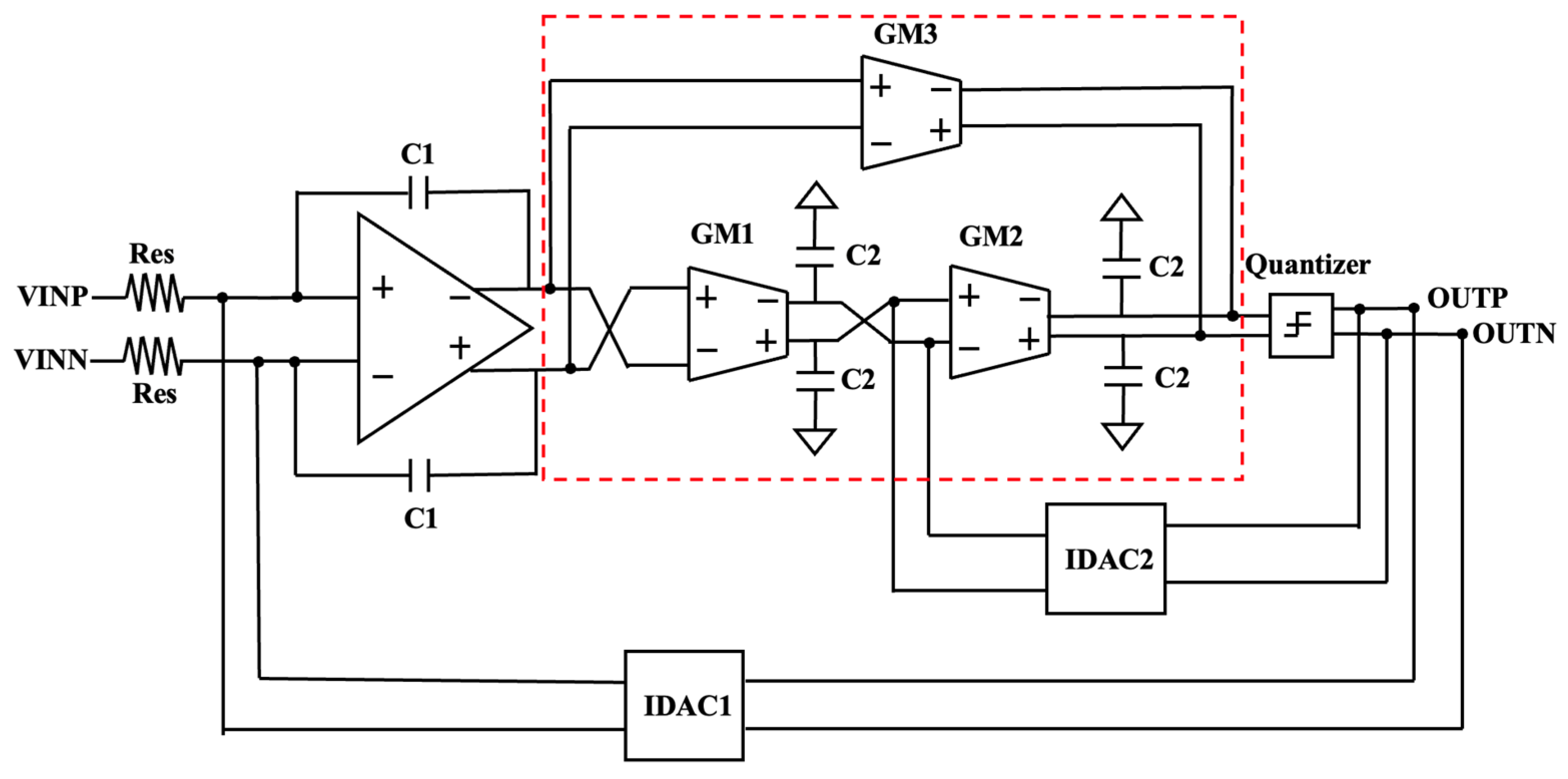
The modulator architecture implemented in this paper is shown in
Figure 5. The first stage integrator is an active RC integrator, followed by GmC amplifiers in the subsequent stage. The two IDACs are return-to-zero structures, essentially composed of current mirror, and the quantizer is 1-bit.
The bias circuit generates a common-mode voltage and current in the circuit. In RF systems, zero-temperature-coefficient current (ZTAT) enables temperature-insensitive biasing, where performance parameters like gain/frequency must remain stable across industrial/automotive temperature ranges (−40 °C to +125 °C). In practical applications, the temperature characteristics of bipolar transistors (BJTs) are commonly used to generate both positive and negative temperature coefficients. Bandgap reference circuits generate ZTAT by combining complementary temperature-dependent currents: a Proportional-To-Absolute-Temperature (PTAT) current and a Complementary-To-Absolute-Temperature (CTAT) current.
Clock jitter in CT-DS modulators directly modulates quantization noise, degrading SNR. When driving high-performance ADCs to process high-frequency input signals, such as in IF and RF sampling applications, using a low jitter clock signal is imperative. Typically, a pure sine wave is used and preferably filtered to reduce wideband noise. The clock signal can be generated using a crystal oscillator or a signal generator. A clock recovery circuit using analog correlation to obtain low jitter data while achieving wide locking range is illustrated in [
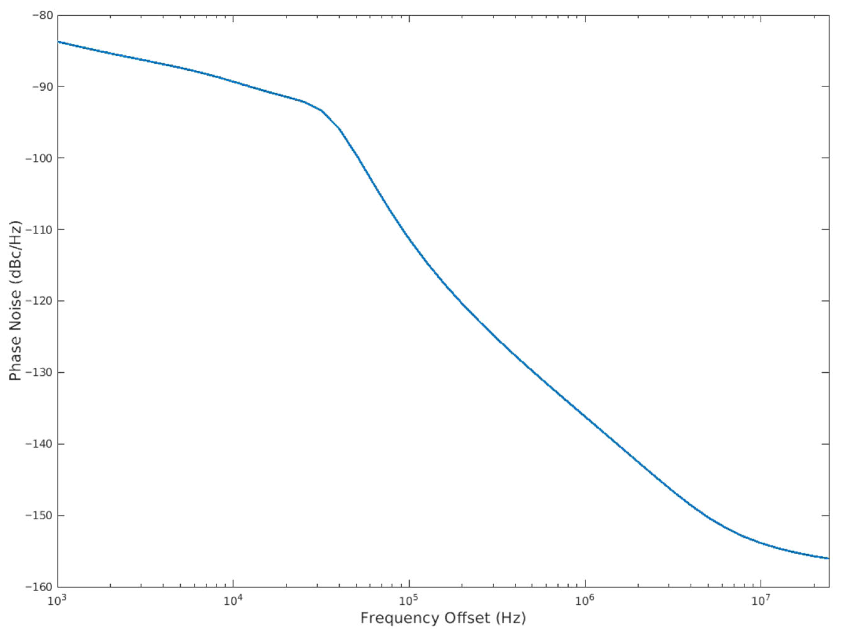
13]. Alternatively, low-jitter clock generation circuits can be used in real applications, where an on-chip phase-locked loop (PLL) is employed to lower the phase noise of the clock signal. The resolution meets the requirements of practical applications by simulation with the phase noise of the PLL, as shown in
Figure 6. The Root Mean Square (RMS) of clock jitter provided by the PLL can be calculated by the phase noise:
where
As is the amplitude of clock signal,
fs is the frequency, ∆
T is the jitter,
is the phase shift, and
L(
f) is the phase noise provided by the PLL. The
Jrms of the clock signal provided by the PLL is 9 ps, and the SNR of the ADC changes with the input signal frequency.
The hybrid RC-GMC integrator topology is used in this design. Two GMC amplifiers are connected in series, and another GMC amplifier is connected in parallel. This structure can achieve a large low-frequency gain and provide a zero point. The core function of Gm3 is to provide a feedforward path, create a critical adjustable zero point, and greatly enhance the performance (stability and noise shaping ability) of the integrator stage in the Sigma Delta modulator loop. The transfer function of three GMC amplifiers in the red box of
Figure 5 is
where
Vin(
s) and
Vout(
s) are the input and output of the three GMC amplifiers in the red box.
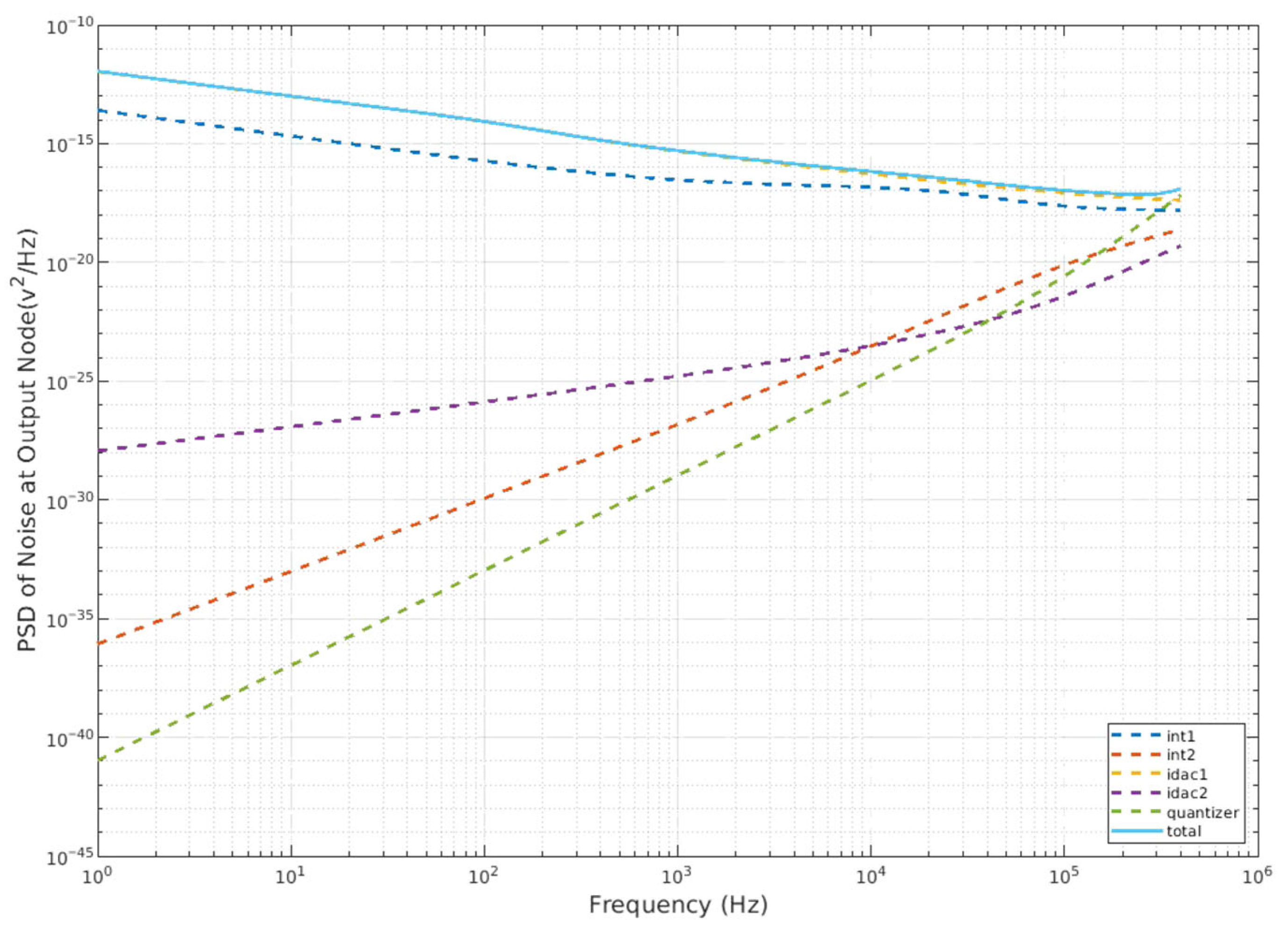
Figure 7 illustrates output-referred noise power spectral density (PSD) of each module, obtained through extensive circuit noise simulations. Before any circuit implementation, we first performed extensive behavioral simulations in MATLAB to optimize loop parameters. This step is important because it defines the fundamental noise-shaping characteristic and stability of the modulator. The figure clearly shows that the first RC integrator and IDAC1 are the dominant noise sources. This is a typical characteristic of a noise-shaping ADC, as the first block’s noise is minimally attenuated by the loop filter. The input transistors of the op-amp are sized to minimize their thermal noise coefficient. The current sources in the IDACs were designed for high output impedance to ensure accurate current steering and minimize noise injection. Specific optimization methods will be described in detail in the following parts.
3.1. Op-Amp
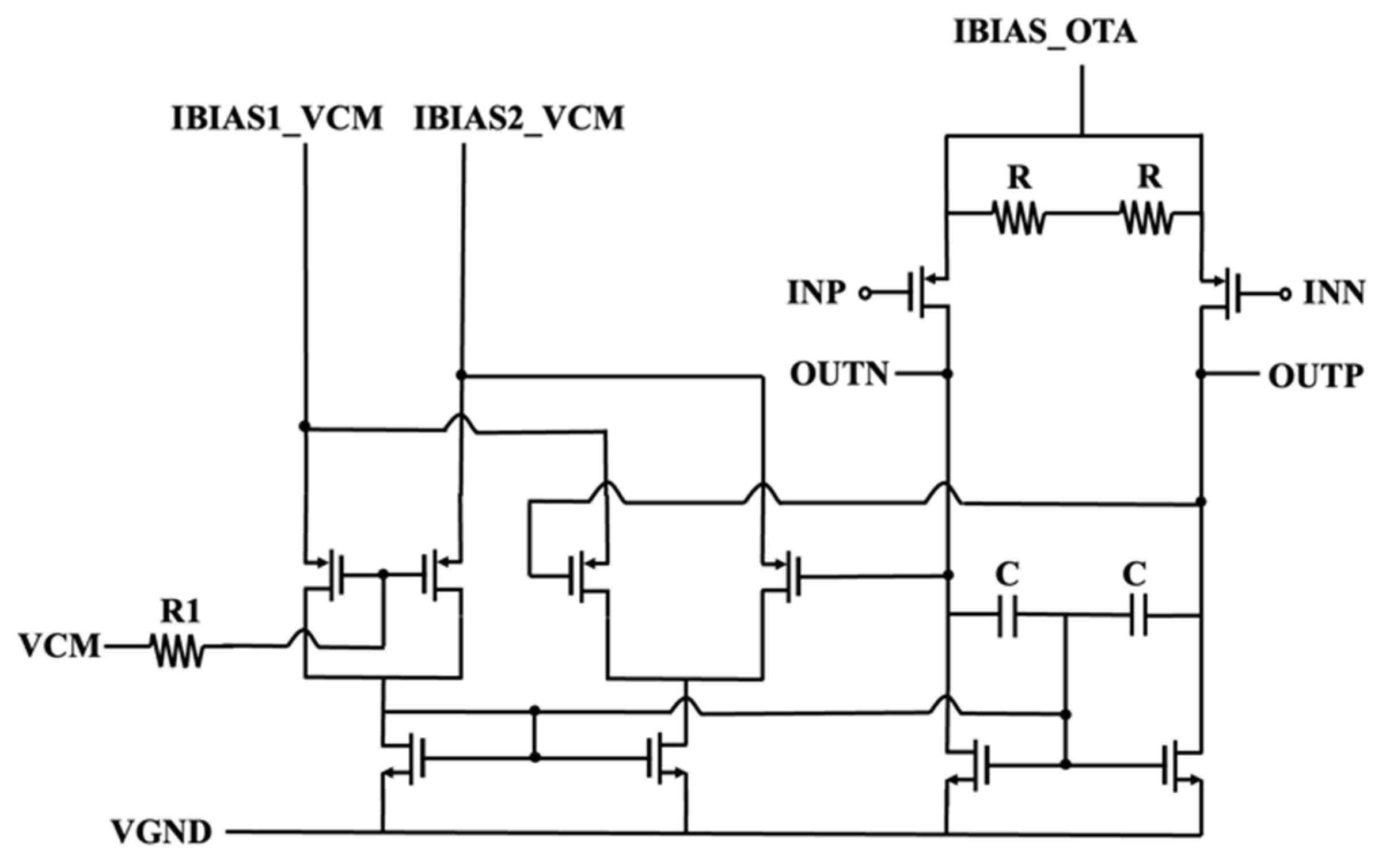
Figure 8 illustrates the OTA op-amp structure used in this circuit. The OTA employs subthreshold-biased input pairs (M1–M2) with large channel dimensions to maximize transconductance efficiency (gm/ID) while operating at a fixed quiescent current of 180 μA. Source degeneration resistors are integrated into the differential pairs of GmC integrator to increase the linearity.
A very common technique used in most MOS OTAs to improve linearity is the resistor source degeneration. The resistors are connected between VDD and the source of the MOS transistor. The signal swing between the gate and the source of the transistor is reduced so that input/output characteristics become more linear. The effective transconductance (Gmeff) is given as follows:
where
gm is the intrinsic transconductance without degeneration. To achieve higher linearity, it is desired to increase both
gm and
R, so that
Gmeff depends primarily on linear resistor
R and non-linear contribution of
gm is minimized.
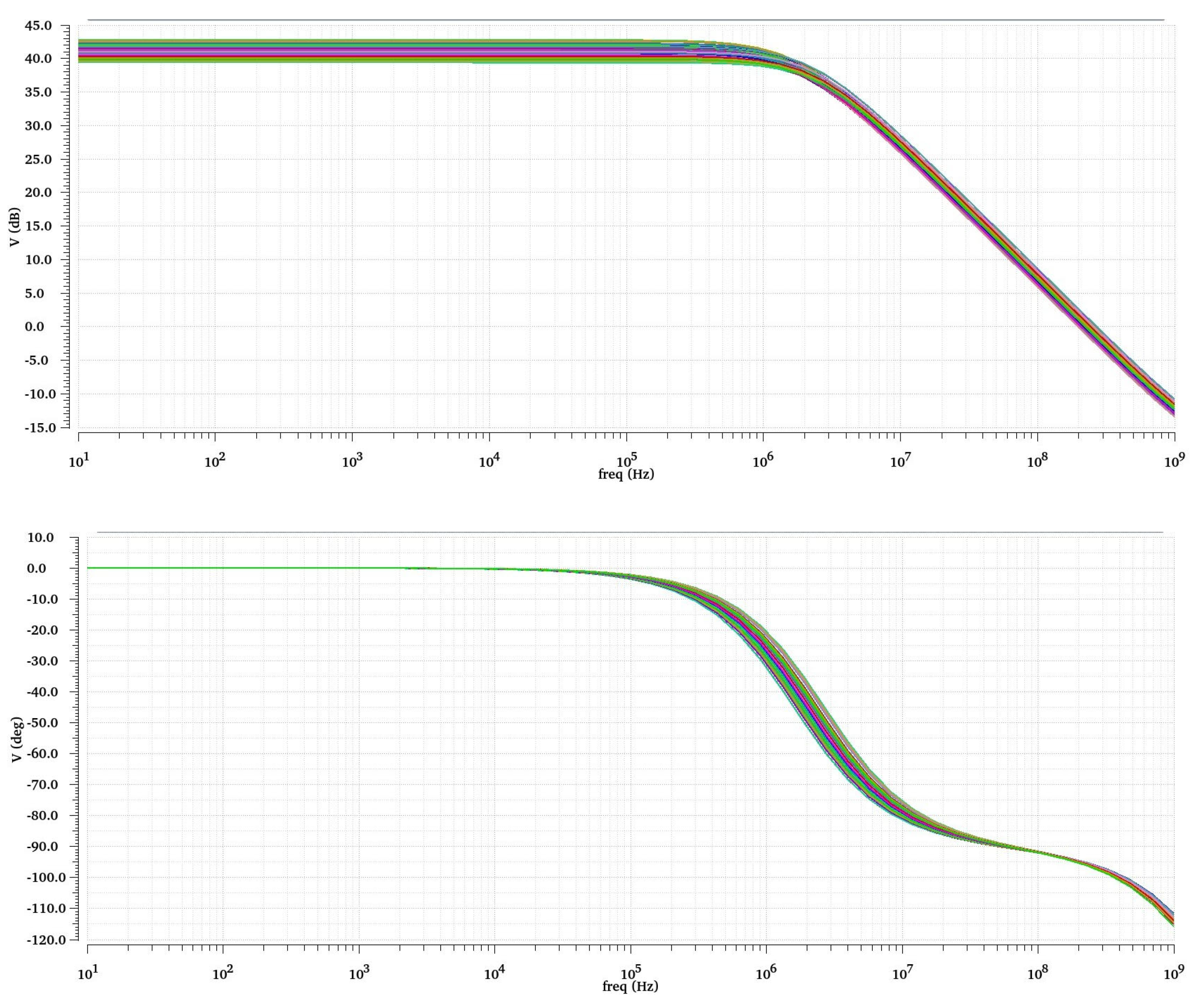
Figure 9 illustrates the performance variations of the amplifier across standard PVT corners, including the Slow-Slow (SS), Typical-Typical (TT), Fast-Fast (FF), Slow-Fast (SF), and Fast-Slow (FS) process corners, a ±10% supply voltage variation, and a temperature range from −40 °C to 125 °C. It is shown that PVT variation can be tolerated in the proposed amplifier.
In conventional common-mode feedback (CMFB) schemes, the common-mode voltage (VCM) is stabilized by directly comparing ICMFB to a reference current (IREF). However, process variations or mismatches in current mirrors can degrade accuracy. The differential feedback current (Idiff) and common-mode feedback current (IVCM) are summed to equal a fixed reference. This ensures that mismatches in current mirrors or process variations are inherently compensated, as deviations in one path are counterbalanced by adjustments in the other. The magnitude of the feedback current and VCM current can be better matched, improving the control accuracy of the common-mode voltage.
Direct-current comparison of the CMFB is inherently sensitive to noise in the ICMFB path, particularly at low frequencies where flicker noise dominates. In the proposed architecture, this results in a reduction in integrated noise. The addition of current can average out the noise and reduce the sensitivity to noise from a single current source. Noise suppression is critical for high-resolution applications such as ΔΣ modulators.
Feedback performance can be optimized in terms of process, voltage, and temperature (PVT) by adjusting the ratio of the addition through programmable current mirrors. If the magnitude of the feedback current and the VCM current does not match, it may lead to comparison errors and affect the accuracy of the common-mode voltage.
The proposed CMFB architecture achieves higher accuracy, lower noise, and greater design flexibility than traditional methods. Its current-mode operation inherently compensates for mismatches and supply variations, making it ideal for high-performance analog front-ends in biomedical, audio, and precision sensor interfaces.
3.2. Integrators
The performance of the operational amplifier used in its loop filter dominates the overall performance of the ADC, especially in DS architectures. As mentioned in [
14,
15], the noise, linearity, and power consumption directly influence the ADC’s effective resolution and energy efficiency. Therefore, lowering the power consumption of operational amplifiers while maintaining sufficient gain and bandwidth is the key design priority.
The gain of Switch Capacitor (SC) circuits is determined by a capacitor ratio, offering high precision due to the superior matching properties of integrated capacitors. However, SC circuits require high-speed switches and clocking systems, which will increase dynamic power. In contrast, the gain of a CT system depends on the RC or GmC product. This can allow for switching noise to be avoided but it requires attention to linearity and stability.
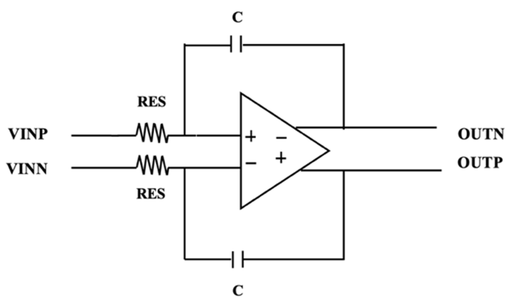
For the first-stage integrator in the loop filter, noise and linearity are crucial. As illustrated in
Figure 10, the active RC integrator shows good advantages in terms of its linearity and higher signal swing [
16], and the gain can be calculated as follows:
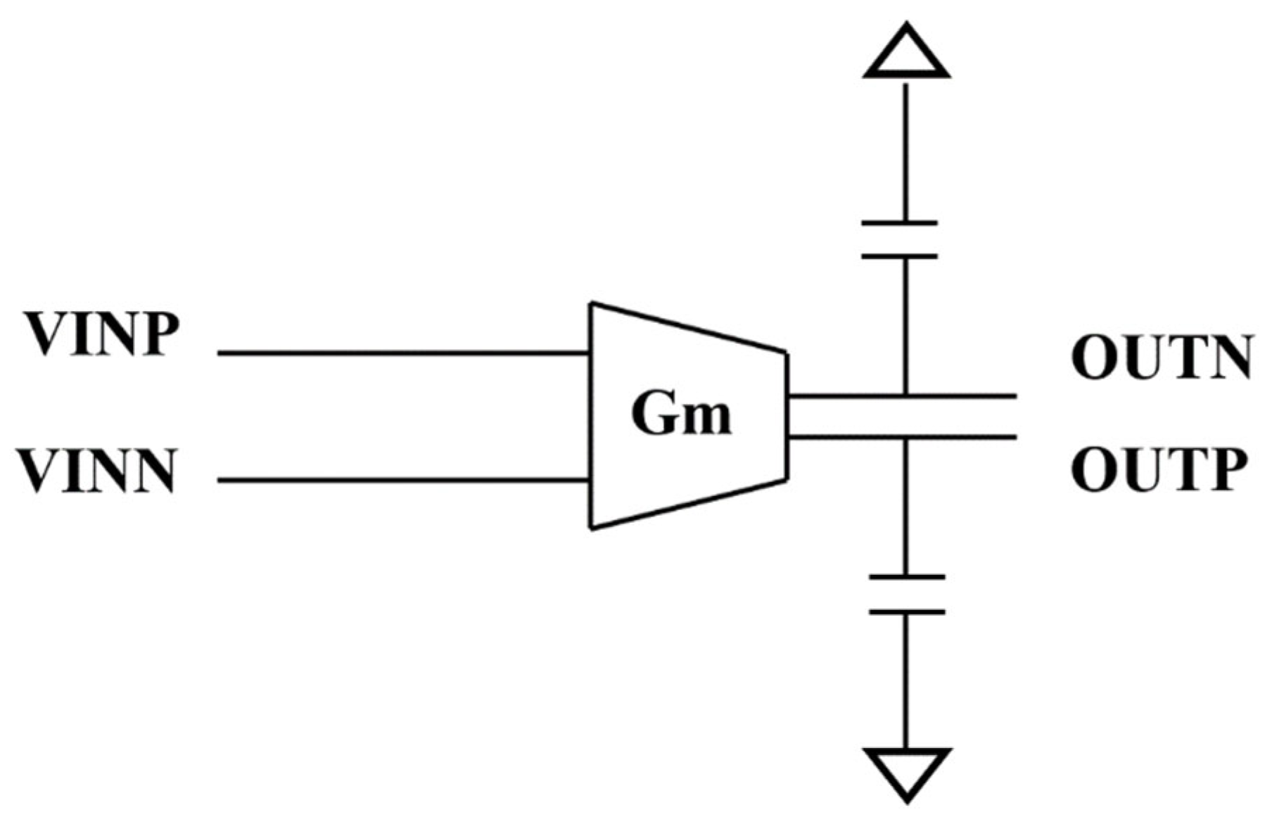
The GmC integrator shown in
Figure 11 is based on a transconductance amplifier and capacitor, which has better mismatch insensitivity and tunability. The minimum signal accuracy that the amplifier can process will be limited and the linearity of the circuit will be deteriorated by mismatch. To improve the gain and unity-gain bandwidth, two GMC integrators are connected in series and then connected in parallel with another GMC integrator.
The gain of the first-stage integrator is 42 dB at a low frequency, while the gain of a GmC integrator is 30 dB. The first-stage integrator provides higher gain and lower noise.
3.3. Quantizer
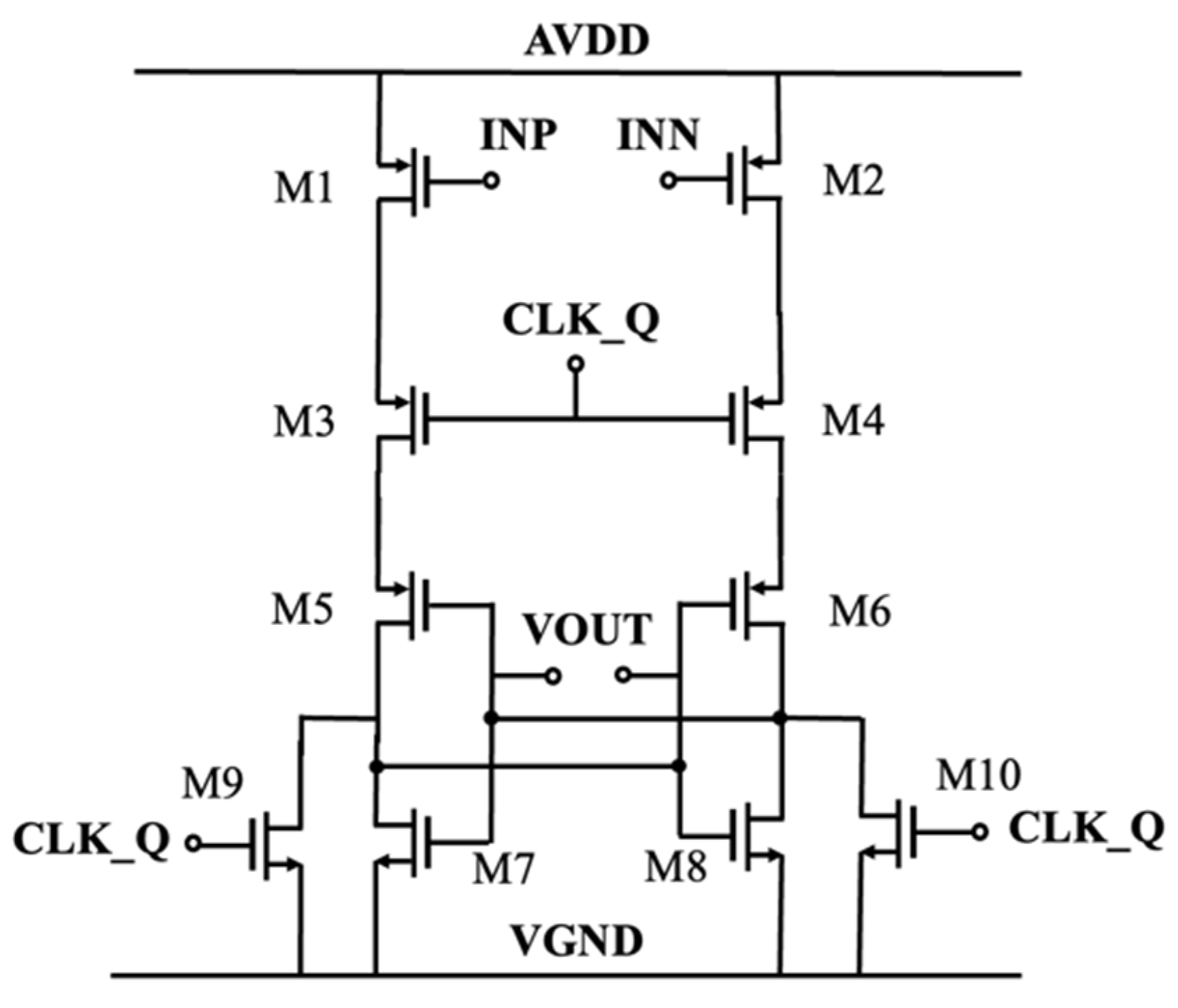
CT-DS modulator can achieve high resolution by using a 1-bit quantizer with noise shaping and oversampling techniques. The quantizer topology based on StrongARM (SA) Latch is shown in
Figure 12. The performance of comparators is mostly affected by input-referred noise and offset voltage [
17]. In most types of ADC, comparators consume a large amount of power and limit the performance of the ADC, including resolution, dynamic range and conversion speed. SA Latch is a typical kind of dynamic comparator which has gained popularity due to its high energy efficiency and high speed. SA Latch is suitable for power-constrained applications as it can achieve a rail-to-rail output within a single clock by regenerating feedback to amplify small differential inputs.
The quantizer presented in this paper employs PMOS input pairs and inserts two switches between inputs (INP/INN) and outputs (VOUT). The use of PMOS input pairs can significantly reduce the thermal noise and flicker noise in the front end of the quantizer and improve the dynamic range. The switches disconnect the direct path during non-working phases and minimize parasitic capacitors at the input nodes, which enhances high-frequency signal response. The clock signal (CLK_Q) controls the switches to make sure that the isolation between inputs and outputs mitigates signal coupling. During the reset phase, switches prevent charge injection from output nodes into input differential pairs, maintaining input offset stability. Current flows only during the regeneration phases, so that power consumption is lower. Input–output isolation via switches protects sensitive nodes from external disturbances.
The size of input transistors M1 and M2 (W:13.8 μM, L:180 nM, gm:533 μS) is large to meet the requirements of offset- and input-referred noise, and the transistors work in the subthreshold zone to achieve low power consumption. Delay is measured by the interval between the clock’s rising edge and the time when the outputs achieve VDD/2. The current consumption of quantizer is 30 μA, as the current flows only during the regeneration process.
The quantizer’s outputs control the switch logic of the DAC to ensure charge balance at the integrator input. Matched-charge transfer minimizes harmonic distortion. Loop filter coefficients can be optimized to maintain stability according to the behavioral modeling results, as they affect the feedback accuracy and the dynamic range of the feedback nodes significantly.
3.4. DACs
The nonlinearity of DACs results in the comparable nonlinearity for overall conversion in DS modulators, as the DAC output signal is forced by the feedback loop to follow the input signal accurately. The matching of amplitude and timing among the current cells determines the linearity of the DAC. Dynamic errors and static mismatch can significantly degrade the performance of the DAC, particularly in high-precision applications. The static mismatch can be calibrated, while dynamic errors, such as charge injection and clock feedthrough during the switching phase, are difficult to correct. RZ techniques can be used to de-glitch the data path and reduce these dynamic errors by introducing a reset phase within each clock cycle [
18]. It also makes the modulator less sensitive to excess loop delay [
19].
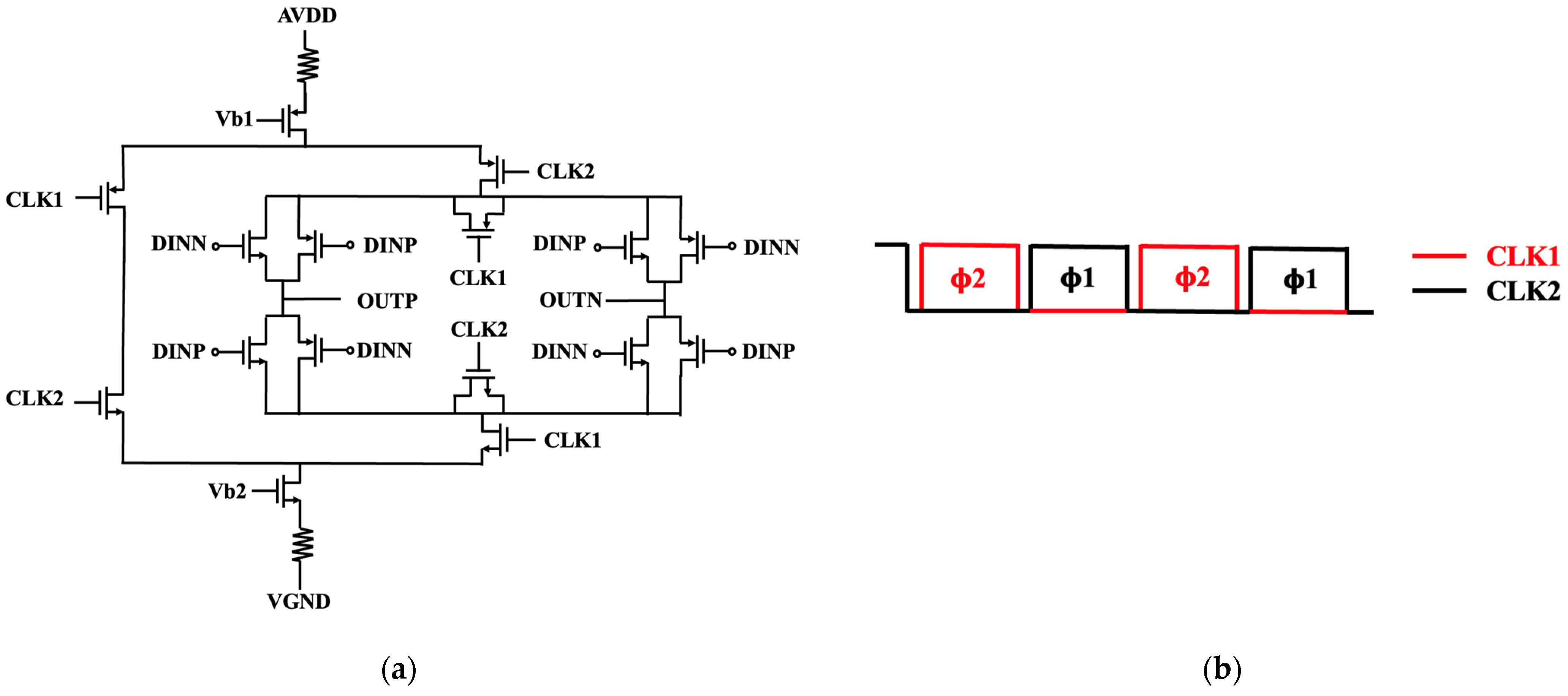
Figure 13 describes the operational process of IDAC feedback. The current value is biased due to Vb1 and Vb2 from the bandgap. CLK1 and CLK2 are non-overlapping clock signals. The IDAC is reset during Φ1. By periodically forcing the output current to zero, regardless of the previous quantizer decision, it breaks the correlation between consecutive DAC output pulses, improving linearity within the modulator’s feedback loop. During Φ2, the quantizer’s differential digital output codes (DINN and DINP) control the differential output switches, which can change the polarity of the current. As the RZ waveform has both a rising edge and falling edge in each clock cycle, unequal rise/fall times will not result in nonlinearity.
Two different techniques used in each IDAC for enhancing current mirror performance are source degeneration and cascode structures. The current mirror used in IDAC1 is shown in
Figure 13a; the input dynamic range of the first stage is large. It primarily leverages negative feedback by adding a resistor in series with the source terminal of the mirroring transistor. This feedback mechanism significantly increases the output impedance and improves the matching accuracy by reducing the sensitivity of the output current to the threshold voltage (V_th) and geometric (W/L) mismatches between the reference and mirror transistors. It also offers enhanced linearity for larger signal swings. However, the resistor contributes additional thermal noise.
The cascode current mirror is used in IDAC2, providing higher output impedance and reducing sensitivity to channel-length modulation (CLM). However, the output voltage range of the cascode is limited and is suitable for IDAC2 as the dynamic range is lower than that of IDAC1.
Source degeneration provides a simpler solution with good matching and moderate performance improvements where voltage headroom is less constrained. Cascode structures are indispensable for applications demanding high output impedance and superior CLM rejection at the expense of complexity and output voltage.
4. Measurement Results
Table 1 summarizes the performance of the CTSD ADC and compares it with that of others based on publications on CTSD modulators or ADCs.
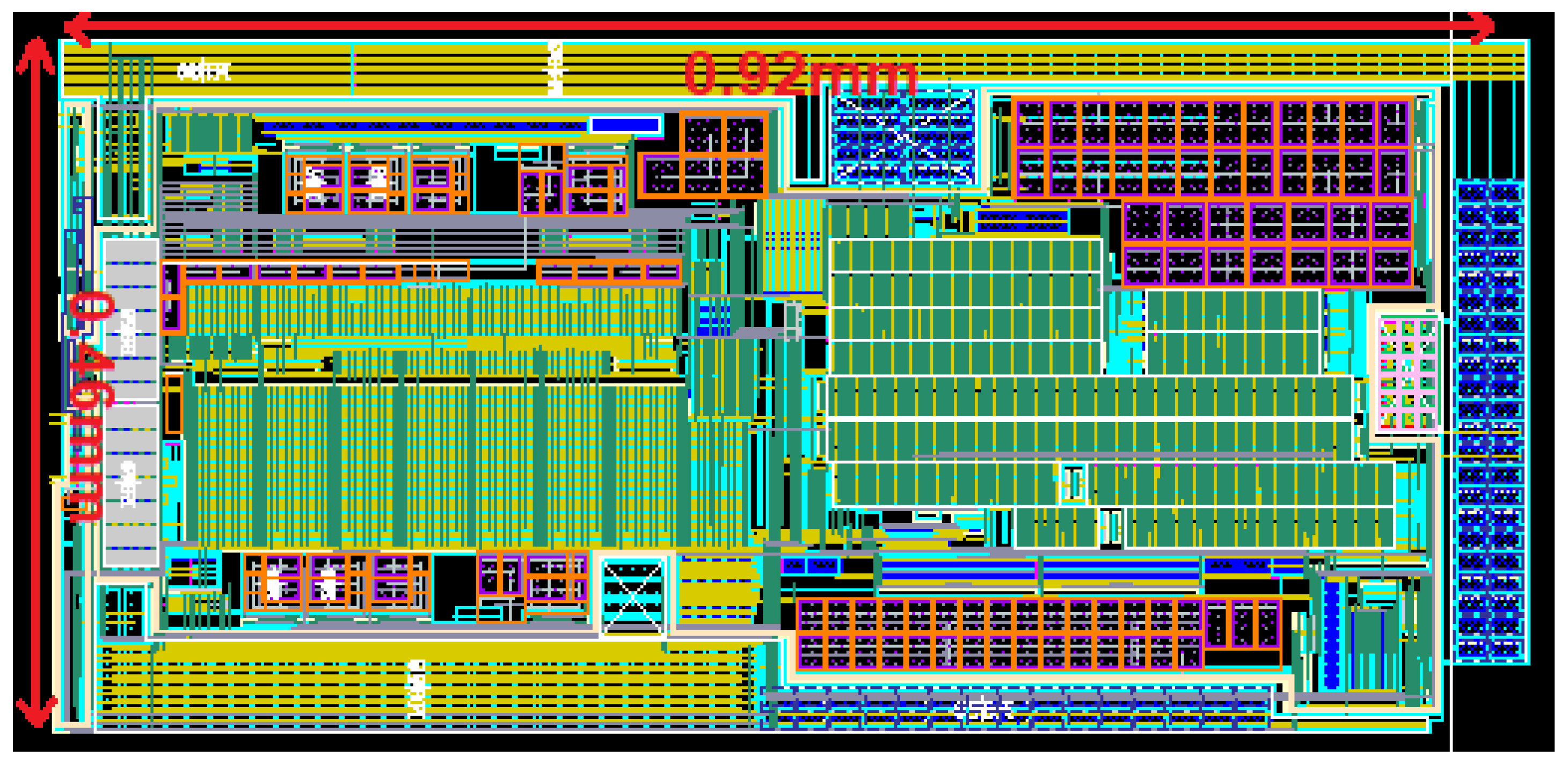
Figure 14 shows the circuit layout of the CT-DS modulator and
Figure 15 illustrates the chip micrograph, fabricated in a 180 nm CMOS process and occupying an active area of 0.42 mm
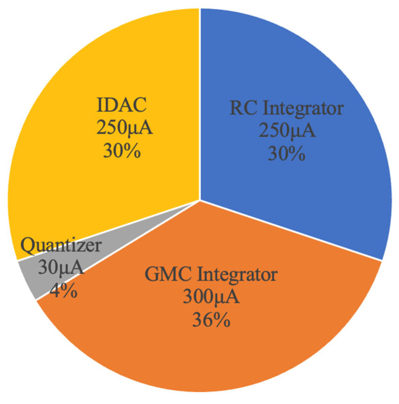
2. The measured total current consumption is 0.8 mA with a 1.8 V supply. The power distribution of the ADC is shown in
Figure 16. The first-stage integrator consumes 30% of the total power, primarily due to its high transconductance requirement for noise and linearity optimization.
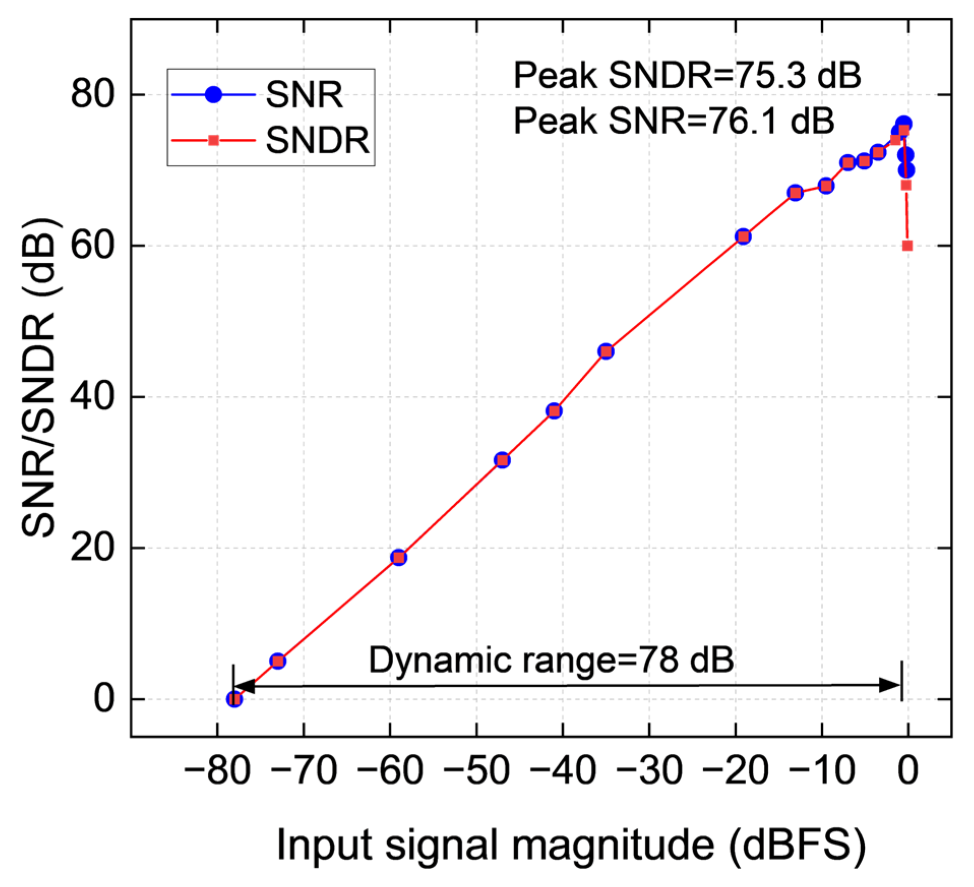
Figure 17 shows the SNDR and SNR as a function of the input signal amplitude with the input signal frequency of 250 kHz. It can be seen that the ADC achieves 78 dB DR, 75.3 dB peak SNDR and 76.1 dB peak SNR.
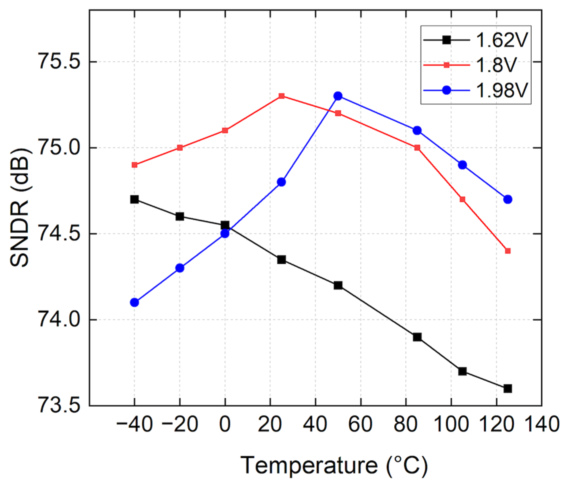
Figure 18 demonstrates the robustness of the presented CTSD ADC against power supply and temperature variations. It can be seen that the SNDR changes by less than 1.7 dB within the −40 °C to +125 °C and ±10% supply variation range. Therefore, the effectiveness of the PVT stabilization scheme is verified. In
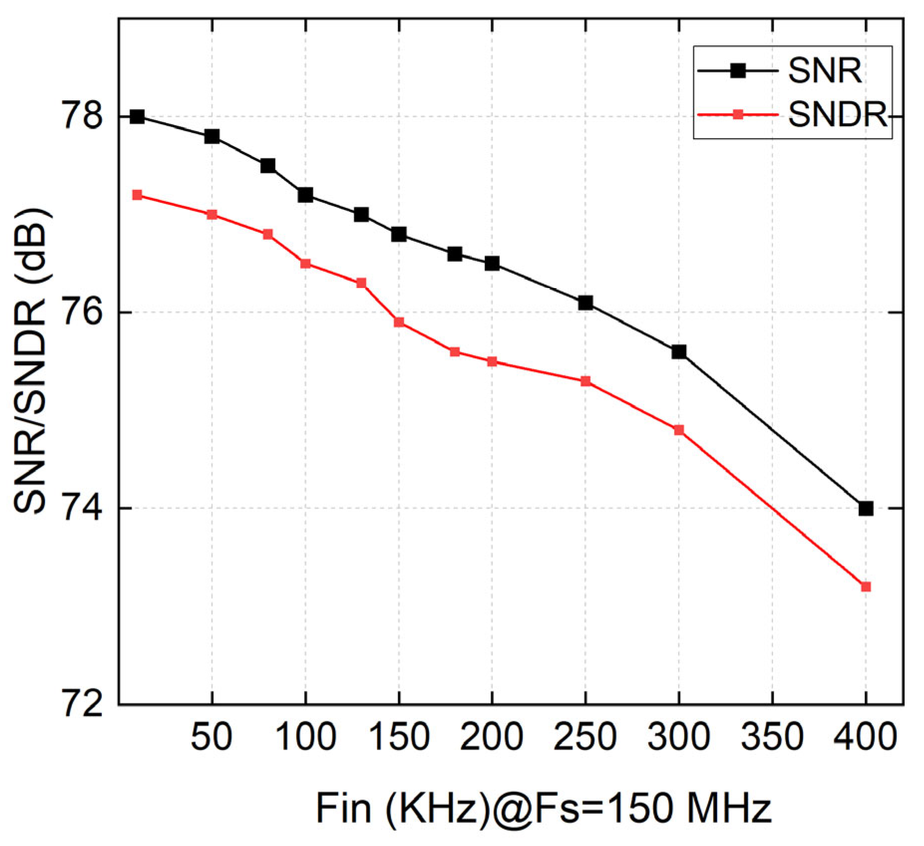
Figure 19, we can see that the SNR and SNDR of ADC decrease as the input frequency increases.
The ADC chip was mounted on a dedicated PCB test board. The board included SMA connectors for analog input and clock signals, decoupling capacitors for all power supplies, and high-speed I/O interfaces for digital data output. A high-precision signal generator provided the input signal, and the on-chip bandgap reference was utilized. The raw modulator bitstream output was captured and processed in MATLAB using a digital decimation filter identical to the on-chip design.
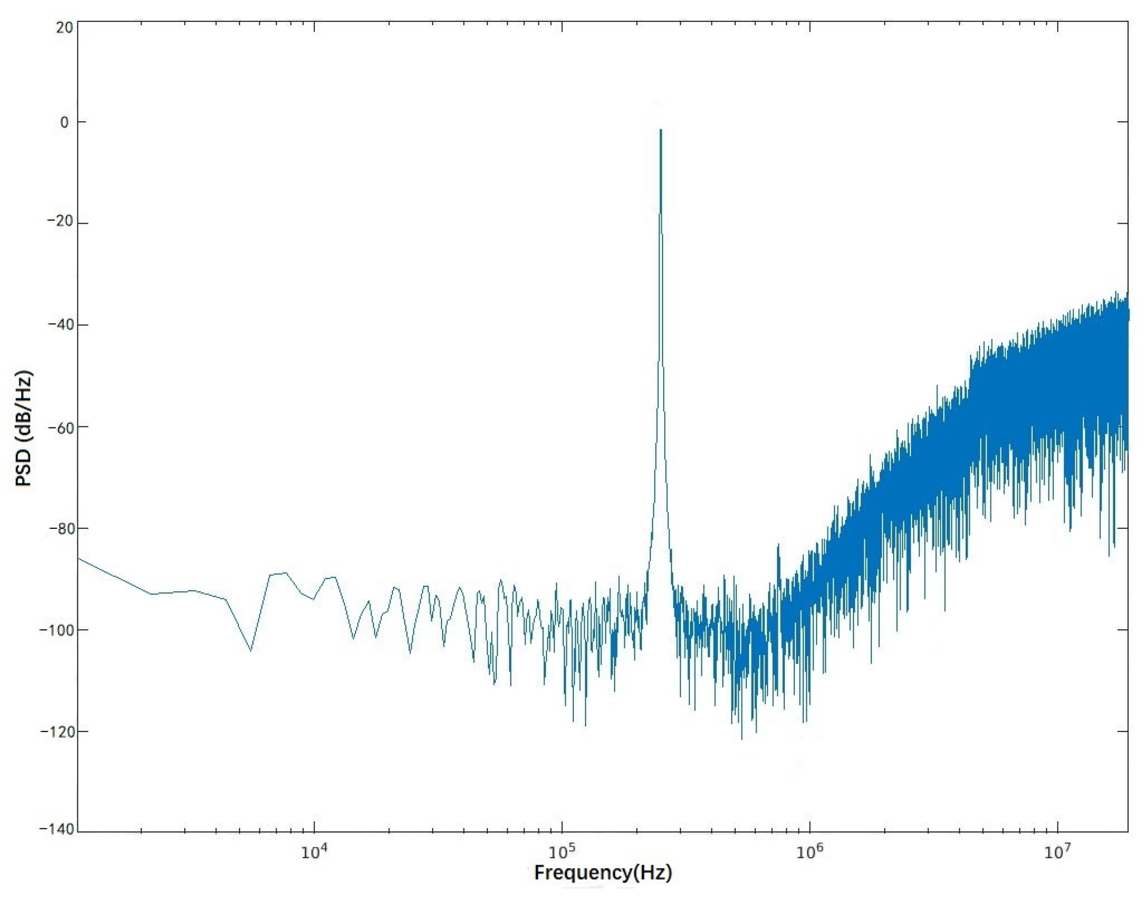
Figure 20 shows the measured output power spectral density of the CT-DS ADC with a 250 kHz −0.5 dBFS input signal. A data record of 2
17 points was collected for analysis, and a Hann window was applied to minimize spectral leakage. The ADC achieves a peak SNR 76.1 dB, and the sensitivity of the receiver is −105.5 dBm. In view of above results, it is concluded that the Schreier FOM based on SNDR is 160.7 dB with a bandwidth of 500 kHz.
The testing was conducted in full compliance with the AEC-Q100-002-REV-E 2013 standard [
20], which defines the Human Body Model (HBM) test method. The temperature of the test was 24 °C and the humidity was 45%. A sample size of six devices per test group was used to ensure statistical significance and result reliability, which were confirmed using a certified, calibrated HBM ESD tester, Thermo Keytek MK2 TE (Thermo Fisher Scientific, Waltham, MA, USA). Each pin was stressed with both positive- and negative-polarity pulses. The “standard step stress” method was followed and the ESD zap interval was 300 ms. The test began at ±500 V and the step voltage was 500 V. Two stringent failure criteria were applied to detect both parametric shifts and failures. A device was considered a failure if the voltage at the reference point (1 μA or IREF) deviated by more than ±30% after ESD testing. This criterion catches changes in internal biasing circuits or reference generators, which are often sensitive to ESD stress. For each pin, we performed a full I-V sweep and established an acceptance envelope (±10%) around the I–V curve before any ESD stress was applied. After each ESD testing, the I–V curve was re-measured. If any part of the new I–V curve fell outside the pre-defined envelope, the device was marked as a failure. This is a very sensitive method to detect any minor damage to protection diodes, junction leakages, or gate oxide impairments that a simple leakage test at one voltage might miss. According to the failure criteria, the ESD sensitivity of the chips can pass the test at ±8000 V. The class is 3B according to the AEC-Q100-002-REV-E 2013 classification.
This CT-DS ADC achieves good FOM in the 180 nm process and demonstrates good stability throughout the entire receiver. It passes relevant automotive-grade tests and meets the requirements of automotive-grade products.
Table 1.
Performance table and comparison to prior work.
Table 1.
Performance table and comparison to prior work.
| Ref. | Tech. (nm) | Area (mm2) | Architecture | Supply (V) | Fs (MHz) | BW (MHz) | SNR | SNDR | Power (mW) | FoM * (dB) |
|---|
| This work | 180 | 0.42 | CT | 1.8 | 150 | 0.5 | 76.1 | 75.3 | 1.44 | 160.7 |
| [21] | 180 | 0.7 | CT | 1.8 | 312.5 | 4.88 | 85.3 | 81.5 | 46.6 | 158.7 |
| [22] | 180 | 0.039 | CT | 1.4 | 500 | 4 | data | 60.23 | 1.92 | 159.2 |
| [23] | 28 | 0.072 | CT | 1.1/1.0 | 500 | 15.625 | 83.9 | 81.6 | 6.4 | 175.5 |
| [24] | 65 | 0.084 | CT | 1.2/1.8 | 400 | 10 | data | 76.7 | 15.1 | 164.9 |
| [25] | 40 | 0.675 | CT | 1.1/1.8 | 2400 | 75 | 68.1 | 67.3 | 38 a | 160.3 a |
| 27 b | 161.7 b |
