1. Introduction
Organic-inorganic halide perovskite solar cells (PSCs) have emerged as a highly promising class of photovoltaic materials due to their exceptional optoelectronic properties [
1]. Since their initial report with a power conversion efficiency (PCE) of ~3% in 2006, PSCs have witnessed rapid progress, reaching certified efficiencies exceeding 26.7% in recent years [
2]. This unprecedented advancement positions PSCs as a strong contender for next-generation solar energy conversion technologies. However, the widespread deployment of lead (Pb)-based perovskites is hindered by the intrinsic toxicity of lead, raising concerns about their environmental and health impacts. As a result, the development of lead-free perovskite materials has become a central research focus [
3,
4,
5,
6,
7,
8,
9,
10].
Among various alternatives, formamidinium tin iodide (FASnI
3, where FA = CH(NH
2)
2+) has gained significant attention as a potential lead-free perovskite absorber. FASnI
3 exhibits several desirable properties, including a narrow direct bandgap of approximately 1.4 eV, high charge carrier mobility, and strong light absorption across a broad spectrum [
11,
12]. Owing to the similarity in valence electron configuration between Sn and Pb—both having two electrons in their outermost shell—Sn can structurally and electronically replace Pb in the perovskite lattice without drastically altering the perovskite framework [
13,
14]. Despite these advantages, Sn-based perovskite solar cells still face critical challenges, particularly regarding material stability and device efficiency. Tin is more prone to oxidation than lead, with Sn
2+ easily oxidizing to Sn
4+, leading to nonradiative recombination centers and poor air stability. Furthermore, Sn vacancies, which form readily due to their low formation energy, further degrade device performance.
FASnI
3 has gained significant attention as a promising lead-free perovskite absorber material, prompting extensive research to improve its photovoltaic performance. Initial reports by Koh et al. [
15] demonstrated a modest PCE of 2.10% for FASnI
3-based PSCs. Subsequent efforts to enhance the material performance have involved compositional engineering and additive strategies. For instance, Ke et al. [
16] introduced phenylethylammonium (PN) and thiophenemethylammonium (TN) into FASnI
3 films, achieving improved efficiencies of 5.85% and 5.53%, respectively. Additionally, further progress was reported with optimized processing of the FASnI
3 absorber, leading to a PCE of 5.4% [
17]. Additional studies have reported enhancements in FASnI
3 absorber properties through various approaches. A mixed-cation strategy involving azetidinium (Az) resulted in AZ
xFA
1−xSnI
3 films with tunable optoelectronic properties and a PCE of 9.6% [
18]. Liu et al. [
19] employed n-propylammonium iodide as an organic additive, achieving a PCE of 11.22% via a spin-coating method. Further improvements have been realized through microstructural control of the FASnI
3 film. Cui et al. [
20] fabricated films with micrometer-scale grains, yielding a PCE of 12.11%. Nishimura et al. [
21] demonstrated over 13% PCE in Sn halide-based devices, underscoring the viability of this material system. Abdelaziz et al. [
22] conducted optical simulations to optimize device parameters, reporting a PCE of 14.03%. Most notably, a fully optimized FASnI
3-based PSC design has been reported to reach a PCE of 19.08% [
23]. In addition to absorber optimization, recent studies have explored the role of hole transport layers (HTLs) in improving device performance. Numerical simulations using SCAPS-1D have revealed the significant influence of different HTL materials on the photovoltaic parameters of FASnI
3-based devices [
24].
The development of hole transport layer (HTL)-free PSCs has attracted growing interest due to their simplified architecture and potential for improved stability. The first HTL-free PSC was reported by Etgar et al. [
25] using the architecture FTO/compact-TiO
2/TiO
2 sheets/MAPbI
3/Au, achieving a PCE of 5.5%. In this configuration, the gold electrode was placed in direct contact with the perovskite layer, which led to device degradation due to gold diffusion into the absorber. To address this issue, more stable carbon-based electrodes became the preferred alternative. For instance, Yang et al. [
26] employed candle soot as a carbon electrode in devices with the structure FTO/compact-TiO
2/mesoporous-TiO
2/MAPbI
3/candle soot, resulting in an improved PCE of 11.2%. Further, Mousoi et al. [
27] investigated the influence of the antisolvent on the performance of HTL-free PSCs using a sandwich structure of glass/FTO/compact-TiO
2/mesoporous-TiO
2/MAPbI
3/Au, achieving a PCE of 5.65%. Njema et al. [
28] numerically presented a novel high-performance HTL-free PSC with the configuration ITO/PC
61BM/CH
3NH
3SnI
3/Pt. The study focused on optimizing electron transport materials, metal back contacts, front contact materials, and, in particular, the integration of various buffer layers—such as cadmium sulfide (CdS)—to enhance the device performance. The optimized cell model achieved a notable PCE of 38.11%. There is a strong demand for HTL-free perovskite solar cells that combine high efficiency with simple fabrication and low-temperature processing.
Computational modeling has become a crucial tool for accelerating the design and optimization of next-generation photovoltaic devices. Methods such as finite-difference time-domain (FDTD) and finite element simulations allow researchers to explore light–matter interactions at the nanoscale. Additionally, drift-diffusion models and device solvers can predict charge transport behavior. These techniques reduce the experimental overhead and enable rapid prototyping of advanced architectures, including nanostructured, HTL-free perovskite solar cells. In this study, the finite-difference time-domain (FDTD) as the computational approach is employed to investigate the optical performance limits of a photonic HTL-free PSC design.
This study presents a numerical analysis of a novel, eco-friendly PSC design based on FASnI
3 nanoparticles. The proposed architecture incorporates a 2D photonic crystal (PhC) structure integrated with a cylindrical titanium dioxide (TiO
2) electron extraction layer and utilizes an HTL-free configuration to simplify fabrication and reduce cost. The optical behavior of the design is systematically investigated using the FDTD method (Ansys Lumerical 2025 R1.3, Lumerical Solutions, Inc., Vancouver, BC, Canada) [
29]. Simulation results reveal a notable enhancement in ultimate efficiency exceeding 16% compared to conventional planar designs. To understand the mechanisms underlying this improvement, the electromagnetic field distribution within the device is analyzed. The observed absorption enhancement is attributed to the strong coupling of photonic modes with surface plasmon polaritons. Moreover, the spectral absorption remains nearly independent of polarization and incident angle, maintaining high performance for both TM and TE polarizations up to an angle of 60°. The influence of key geometric parameters of the 2D photonic structure on device efficiency is also explored, highlighting the potential for further optimization.
2. Design Considerations
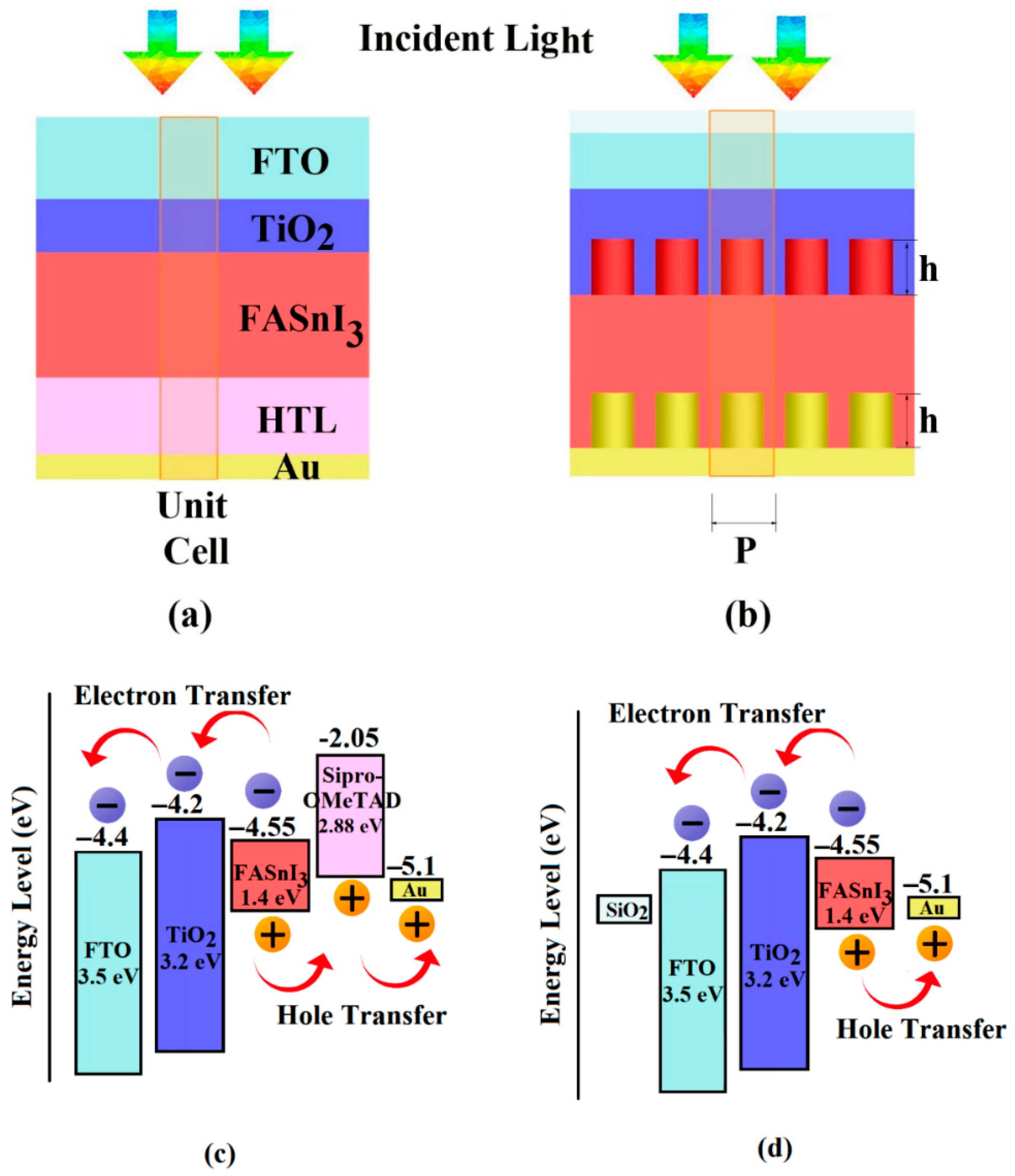
Schematic representations of the conventional planar PSC and the proposed 2D PhC structure incorporating FASnI
3 as the active absorber layer are presented in
Figure 1. FASnI
3 is a promising candidate for environmentally friendly PSCs due to its direct bandgap of 1.41 eV, offering strong light absorption in the visible spectrum. Additionally, its high thermal stability and relatively large bandgap make it a durable and efficient material for photovoltaic applications.
The conventional PSC architecture, illustrated in
Figure 1a, consists of a transparent conductive oxide (TCO) layer—specifically fluorine-doped tin oxide (FTO)—with a thickness of 500 nm. This is followed by a 60 nm layer of titanium dioxide (TiO
2) serving as the electron transport layer (ETL). The absorber layer is composed of a 350 nm film of FASnI
3. A 200 nm thick p-type layer of Spiro-OMeTAD acts as the hole transport layer (HTL), and a gold (Au) layer is used as the back contact, providing reflectivity and blocking light transmission. The corresponding energy band alignment for this planar configuration (FTO/TiO
2/FASnI
3/Spiro-OMeTAD/Au) is shown in
Figure 1c.
The proposed novel PSC design, shown in
Figure 1b, incorporates a 2D photonic crystal structure within the FASnI
3 absorber layer. This PhC is realized as a periodic array of TiO
2 cylindrical nanostructures, arranged in a 4×4 lattice. Each cylinder has a height of h = 30 nm and a radius of r = 50 nm. In this configuration, the device operates without an HTL layer, relying instead on a conformal gold layer to serve as the back contact. The HTL-free architecture simplifies the device fabrication process, reduces production cost, and minimizes interfacial recombination by eliminating potential instability introduced by organic HTL materials. Accordingly, the simplified layer stack for the proposed HTL-free design is FTO/TiO
2/FASnI
3/Au, as illustrated in
Figure 1d, which presents the corresponding energy band alignment for the structure. This structural modification not only enhances light trapping through photonic and plasmonic effects but also offers a scalable and low-cost approach for fabricating high-performance lead-free PSCs.
The optical characteristics of the proposed and reference perovskite solar cell designs are investigated using the FDTD method, implemented via commercial software (Lumerical Solutions, Inc.) [
29]. A normally incident plane wave, propagating perpendicular to the x–y plane, is employed to simulate solar illumination across a wavelength range of from 300 to 900 nm.
To reduce computational complexity, a single unit cell of the photonic crystal structure is modeled, with a periodic hole pitch of 125 nm in both the x and y directions, as shown in
Figure 1b. Periodic boundary conditions (PBCs) are applied in these lateral directions to simulate an infinitely repeating structure. In the vertical direction (
z-axis), perfectly matched layer (PML) boundary conditions are implemented at both the top and bottom of the simulation domain to eliminate spurious reflections and emulate an open-boundary condition. For simulations involving oblique incidence, Bloch boundary conditions are employed in the x and y directions to account for wavevector components parallel to the surface.
This optical modeling framework is employed to comprehensively evaluate the performance of the proposed 2D PhC-based HTL-free perovskite solar cell. The simulation workflow is structured in three main stages to ensure a thorough understanding and optimization of the device’s optical behavior. First, the photonic crystal geometry is systematically optimized to enhance light absorption within the FASnI3 active layer. The radius, height, and periodicity of the TiO2 cylindrical nanostructures are adjusted to identify configurations that support resonant light trapping and constructive interference, thereby maximizing the ultimate efficiency. Second, the spatial distribution of the electromagnetic field and the wavelength-dependent optical generation rate are analyzed to elucidate the physical mechanisms driving absorption enhancement. This includes evaluating the excitation of photonic modes and the coupling of incident light into surface plasmon polariton (SPP) modes at the perovskite–metal interface, as well as examining field confinement within the photonic crystal cavity. These analyses offer insight into how structural resonances enhance light–matter interaction. Third, the influence of critical design variables on device performance is investigated to assess the robustness and tunability of the PhC-enhanced structure. Parameters such as the incident light angle, polarization state (TE/TM), and lattice symmetry are examined to determine their effects on absorption efficiency and angular/polarization insensitivity. This comprehensive modeling strategy enables a quantitative comparison between the proposed and conventional architectures and serves as a foundation for guiding the design of high-efficiency, scalable, and environmentally friendly HTL-free perovskite solar cells.
The optical performance of the proposed 2D PhC-HTL-free perovskite solar cell design is optimized to enhance light absorption and, consequently, the ultimate efficiency. Optical simulations are performed using the FDTD method implemented in the Lumerical software package [
29].
The wavelength-dependent absorbed power,
, is calculated as follows:
where
denotes the reflectance, obtained from a frequency-domain monitor placed at the top surface of the device, and
represents the transmittance of the design. In this configuration, transmission is negligible due to the opaque gold (Au) back contact, hence
.
The theoretical maximum efficiency, also referred to as the ultimate efficiency
, assumes ideal conditions with no recombination losses and a perfect conversion of absorbed photons into electron–hole pairs. It is calculated using the following expression [
30,
31]:
Here,
is the incident wavelength,
is the cutoff wavelength corresponding to the bandgap of the absorber layer, and
is the spectral photon flux density from the standard AM 1.5 solar spectrum [
32,
33]. In this study,
= 886 nm, corresponding to the bandgap energy of FASnI
3.
The short-circuit current density,
, is calculated based on
, Planck’s constant
, the elementary charge
, and the speed of light
, as follows [
34]:
In addition, the optical generation rate G(λ) represents the number of electron–hole pairs generated within a semiconductor material per unit volume and per unit time as a result of the absorption of incident light at a specific wavelength λ. This rate depends on the material’s optical properties, the intensity and wavelength of the incoming light, and the absorption coefficient at that wavelength. The G(λ) is given by the following:
where
is the speed of light in a vacuum.
These equations provide the fundamental framework for analyzing and optimizing the optical absorption behavior and overall photovoltaic efficiency of the proposed 2D PhC structure without HTL.
3. Numerical Results and Optical Performance Analysis
3.1. Optical Absorption and Device Performance
Figure 2 presents the wavelength-dependent optical absorption spectra for both the conventional planar perovskite solar cell (PSC) and the proposed 2D photonic crystal (PhC) HTL-free design. As evident from the results, the 2D PhC-HTL-free design exhibits significantly enhanced optical absorption across the entire visible spectrum compared to the conventional structure.
The simulated performance metrics reveal that the 2D PhC-HTL-free design achieves an ultimate efficiency of 42.3% and a short-circuit current density of 27.2 mA/cm2, whereas the conventional PSC attains an efficiency of 36.6% and This corresponds to a performance enhancement of more than 16% in favor of the proposed structure. Additionally, when comparing planar designs with and without the HTL, the HTL-free configuration slightly outperforms the one with HTL, achieving an efficiency of 40.9% and .
It is also noteworthy that the theoretical maximum ultimate efficiency for FASnI3-based PSCs is approximately 46%, with a corresponding maximum photocurrent density of . The performance of the proposed design approaches these ideal values, highlighting its potential for high-efficiency, eco-friendly solar energy harvesting.
The proposed HTL-free photonic design has theoretically demonstrated an ultimate efficiency of 42.3%. However, the experimental efficiency remains lower due to several non-ideal factors, including interface defects, series resistance, contact-related limitations, and non-radiative recombination losses. Notably, the absence of a hole transport layer can exacerbate challenges related to charge extraction and interface-induced recombination, particularly at the perovskite–metal interface.
To bridge the gap between theoretical and experimental performance, a range of strategies can be employed. Surface passivation techniques—such as the use of self-assembled monolayers (SAMs) or atomic layer deposition (ALD) of thin dielectric films—can effectively mitigate interfacial trap states. Additionally, contact engineering can improve energy level alignment and reduce contact resistance in HTL-free architectures. Materials such as molybdenum oxide (MoOx), nickel oxide (NiOx), or doped graphene have shown promise in this context. Furthermore, the photonic design can be refined to preserve optical enhancement while accounting for practical material constraints.
These measures, taken together, have the potential to significantly reduce the discrepancy between simulated and experimental results, thereby advancing the development of high-efficiency HTL-free perovskite solar cells.
Figure 2b,c illustrates the spatial profile of the optical generation rate within the device for both the conventional and proposed structures. As shown in
Figure 2b, the optical generation rate in the 2D PhC-HTL-free design is notably higher, confirming superior light confinement and absorption enhancement. This improvement is primarily attributed to the excitation of multiple resonant optical modes, including Bloch modes, cavity modes, and surface plasmon polaritons, which collectively enhance light-matter interaction in the active region.
In terms of photocurrent generation, the conventional planar design yields a calculated value of , while the proposed 2D PhC-HTL-free structure achieves , again demonstrating an enhancement of over 16%.
The operation of the HTL-free mechanism can be described as follows: In the conventional planar configuration, the FASnI
3 perovskite absorber generates electron–hole pairs upon illumination. Electrons are extracted via the electron transport layer (ETL), while holes are transported through the HTL toward the anode. In contrast, the HTL-free design eliminates the hole transport layer by directly interfacing the active FASnI
3 layer with a conformal gold (Au) electrode, as depicted in
Figure 1b,d. This structural simplification enables direct hole extraction at the FASnI
3–Au interface, reducing complexity and material cost while maintaining efficient charge separation and collection.
The proposed novel design is assumed at the FASnI
3–Au interface, without the use of a conventional HTL. This assumption is supported by the close energy alignment between the valence band maximum (VBM) of FASnI
3 (~4.55–5.2 eV) and the work function of gold (~5.1–5.4 eV), as shown in
Figure 1d. Similar HTL-free architectures have been demonstrated in lead-free perovskites, including FASnI
3 [
35,
36,
37]. However, direct metal–perovskite interfaces may introduce interfacial recombination due to unpassivated defect states or insufficient band offset selectivity. In experimental implementation, several strategies may be employed to reduce this recombination by introducing a thin interfacial buffer layer (e.g., MoOx or self-assembled monolayers). This buffer layer is to enhance selectivity and reduce recombination. These approaches enable effective charge extraction while maintaining the simplified HTL-free architecture envisioned in our simulation.
3.2. Physical Mechanism of Absorption Enhancement
To elucidate the underlying physical mechanism responsible for the observed absorption enhancement, the electromagnetic field distributions were analyzed.
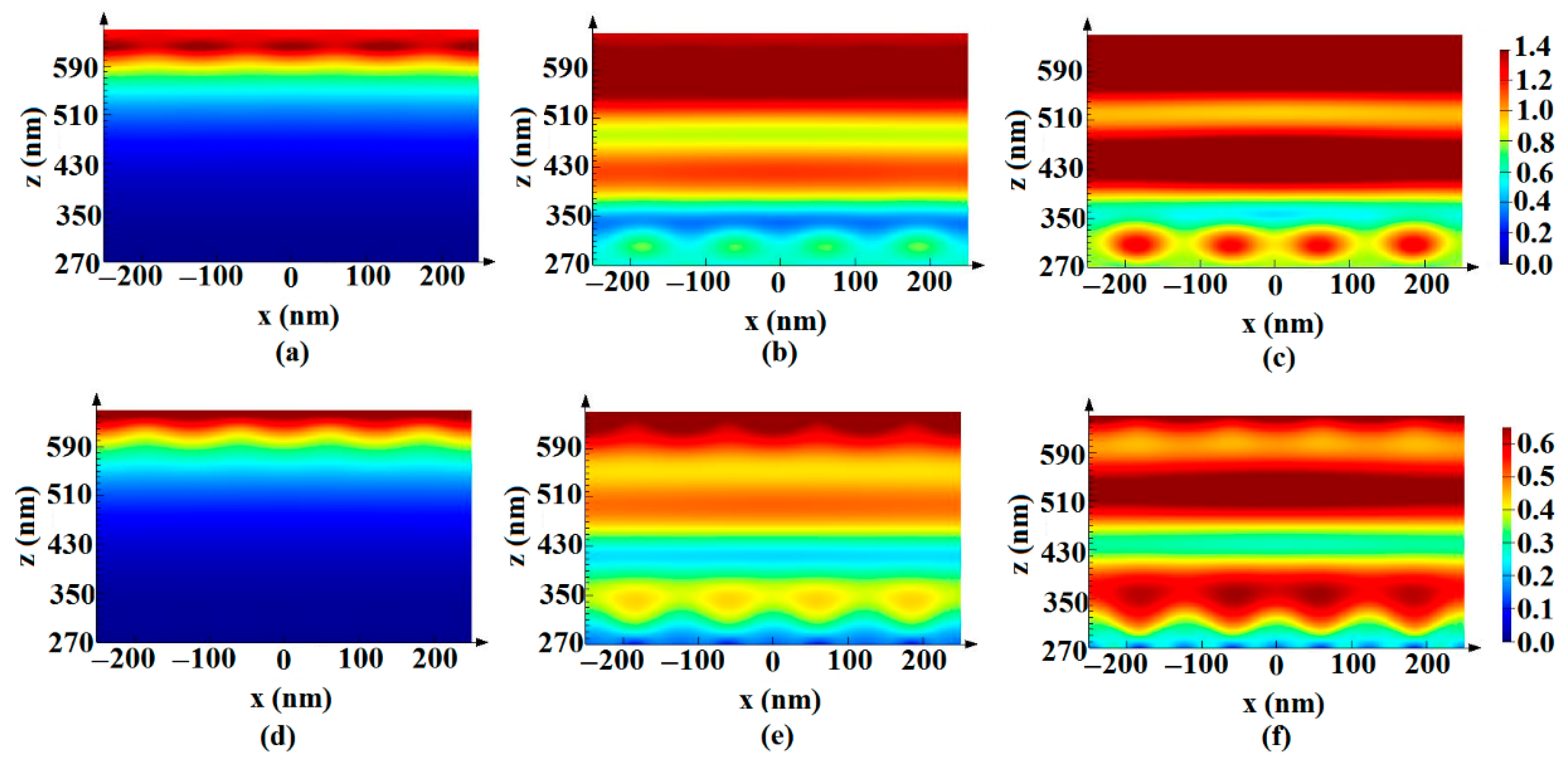
Figure 3 presents the amplitude distributions of the magnetic field (|H|) and electric field (|E|) in the x–z plane under normal incidence at three representative resonant wavelengths: λ = 475 nm, λ = 735 nm, and λ = 820 nm. The magnetic field distributions for the proposed 2D PhC-HTL-free structure are shown in
Figure 3a–c, corresponding to the aforementioned wavelengths, while the corresponding electric field distributions are illustrated in
Figure 3d–f.
As seen in
Figure 3, the intensity and localization of electromagnetic fields within the photoactive layer increase significantly with longer wavelengths. In particular, enhanced field confinement is observed at λ = 735 nm and λ = 820 nm compared to λ = 475 nm, indicating stronger light–matter interaction at these wavelengths. This enhancement contributes to increased absorption within the active layer at longer wavelengths.
Furthermore, as the wavelength increases from λ = 735 nm to λ = 820 nm, both the magnetic and electric fields exhibit pronounced localization around the rear-side Au cylinders. This behavior can be attributed to dipole-like localized surface plasmon resonance (LSPR) effects. Additionally, within the photoactive layer, both Bloch photonic modes and optical cavity modes are excited, while at the perovskite/Au interface, surface plasmon polariton (SPP) modes are also observed.
These findings suggest that the simultaneous excitation of photonic and plasmonic resonant modes plays a crucial role in the enhanced optical absorption observed in the 2D PhC-HTL-free device architecture.
3.3. Angular Dependence of Absorption
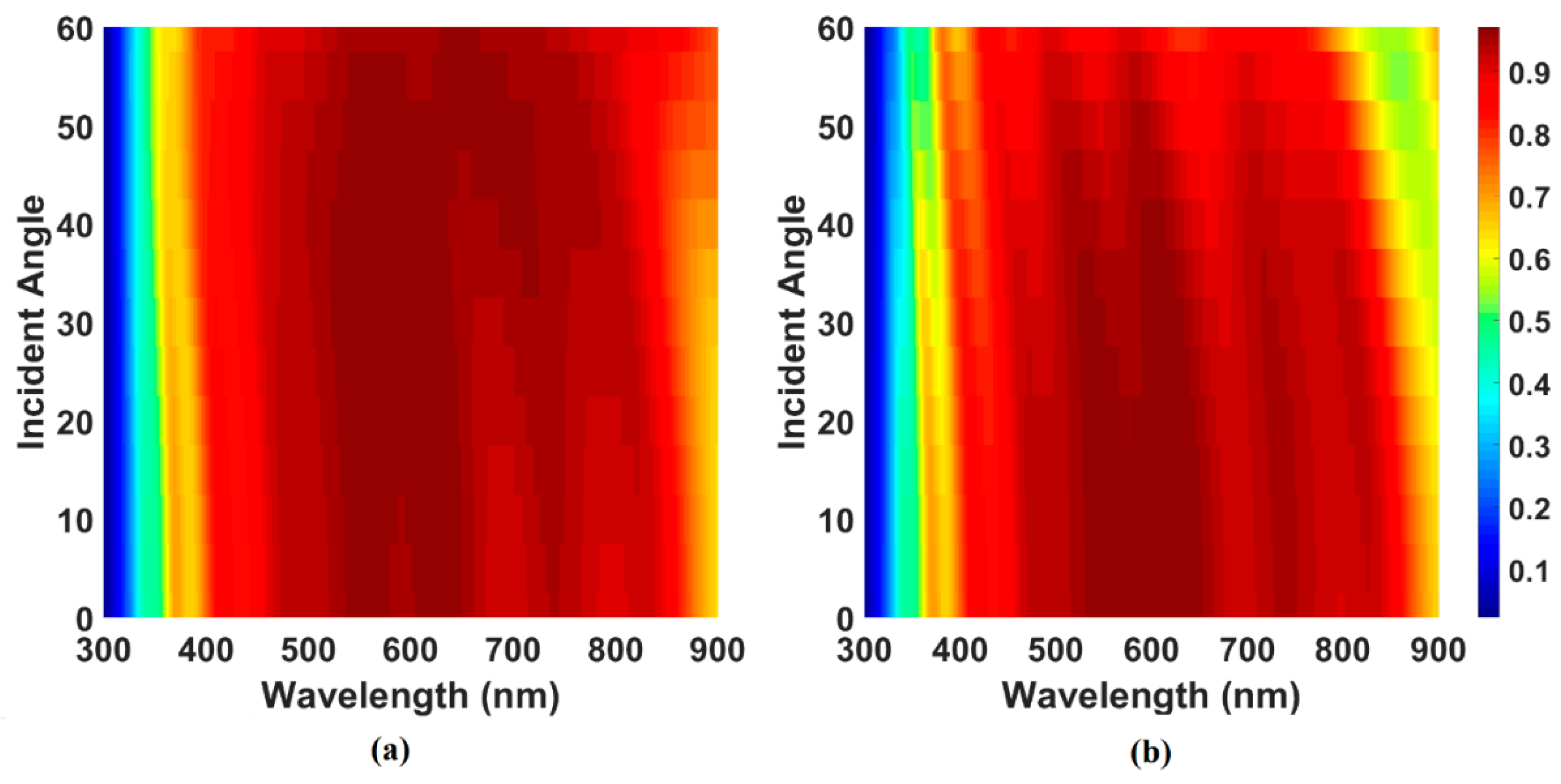
The incident angle of light plays a critical role in determining the absorption characteristics of nanophotonic structures. To evaluate the angular robustness of the proposed design, the absorption spectra of the 2D PhC-HTL-free structure are calculated for both transverse magnetic (TM) and transverse electric (TE) polarized waves as a function of the polar incidence angle.
Figure 4a and 4b illustrate the angle-resolved absorption spectra for TM and TE polarizations, respectively. In the simulation, the incident plane wave is transformed using the Bloch-mode-based finite-angle spectral technique (BFAST), and the periodic boundary conditions are adapted to support Bloch-mode propagation. The results demonstrate that the proposed structure maintains strong absorption performance for both TM and TE polarizations over a broad angular range, specifically from normal incidence (0°) up to 60°.
However, as the incident angle increases beyond 60°, a noticeable weakening of the resonance features occurs, leading to a significant reduction in absorption efficiency. This degradation is attributed to reduced coupling efficiency between the incident light and the resonant modes within the structure at oblique angles. Overall, these findings indicate that the 2D PhC-HTL-free design exhibits angular insensitivity and stable absorption performance for incident angles up to 60°, making it a promising candidate for practical solar energy harvesting applications.
3.4. Polarization Angle Dependence of Absorption
To further assess the optical robustness of the proposed design, the influence of the polarization angle on the absorption spectrum was investigated.
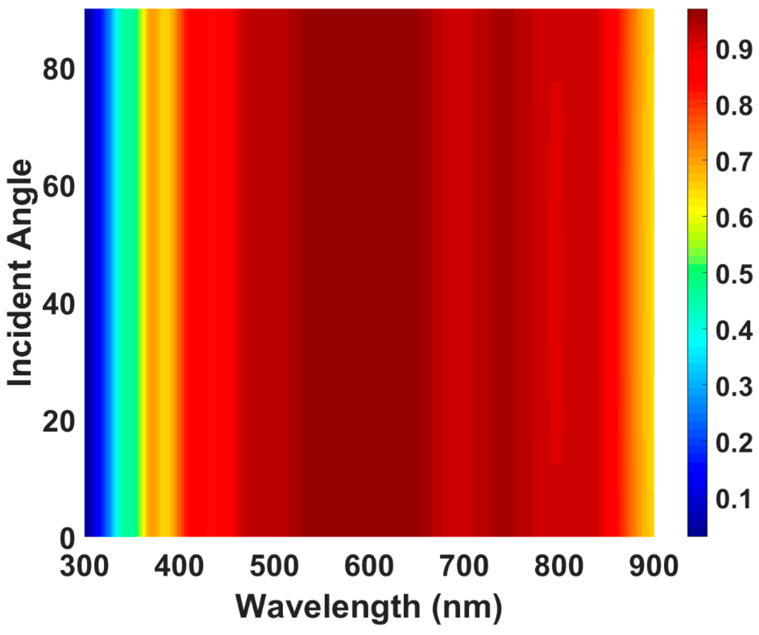
Figure 5 presents the absorption spectra of the 2D PhC-HTL-free structure under normal incidence for varying polarization angles ranging from 0° (TM-polarized) to 90° (TE-polarized). As shown in the figure, the absorption remains consistently high across the entire spectral range of λ = 300–900 nm, regardless of the polarization angle. The nearly identical absorption profiles observed for all polarization angles indicate that the proposed structure exhibits polarization-independent optical behavior. Specifically, the absorption spectra for the two orthogonal polarizations—TM (0°) and TE (90°)—are indistinguishable under normal incidence.
This polarization insensitivity is attributed to the structural symmetry of the 2D PhC-HTL-free design, which ensures that the electromagnetic response does not vary with the orientation of the incident electric field. Consequently, the separation of TE and TM modes by the electric field vector does not influence the absorption characteristics of the device. These results confirm that the proposed structure maintains efficient and stable absorption performance irrespective of the polarization state of incident light, further enhancing its applicability in practical photovoltaic and optoelectronic systems.
3.5. Influence of Geometrical Parameters on Absorption Performance
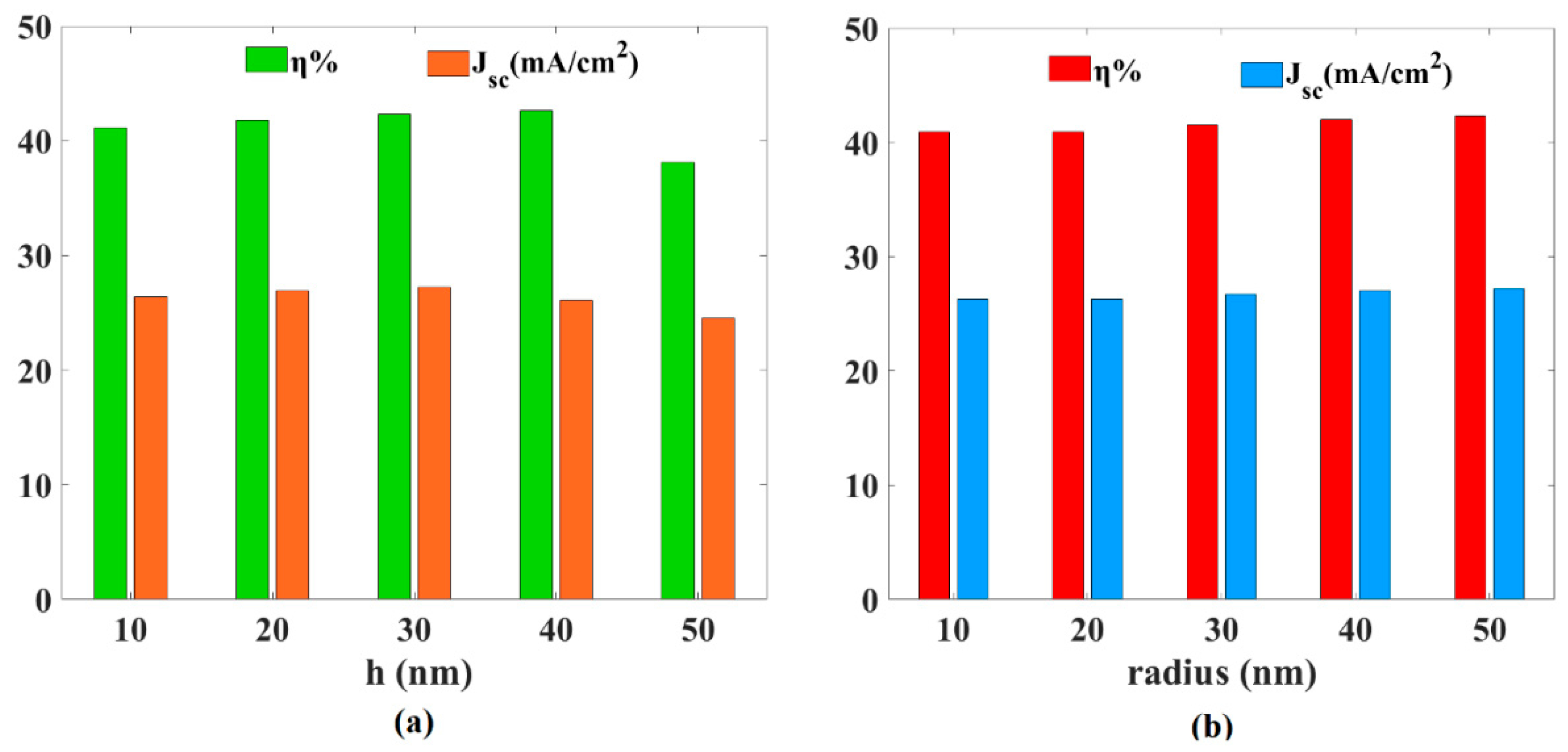
The impact of structural geometry on the optical performance of the 2D PhC-HTL-free design is investigated under normal TM-polarized light incidence. Specifically, the effects of the height (h) and radius (r) of the TiO
2 cylinders are evaluated, with absorption spectra plotted in
Figure 6 over the wavelength range of λ = 300–900 nm.
Figure 6a shows the absorption spectra for different values of height h, varied from 10 nm to 50 nm, while keeping all other parameters constant. As h increases from 10 nm to 30 nm, the average absorption efficiency (
η) improves from 41.0% to 42.3%. However, further increasing the height to 50 nm leads to a decline in efficiency, reducing
η to 38.5%, likely due to optical losses or impedance mismatch.
Similarly,
Figure 6b demonstrates the influence of the cylinder radius. The radius r is varied from 10 nm to 50 nm, resulting in an increase in
η from 40.8% to 42.3%. These results indicate the existence of an optimal geometrical configuration that maximizes light absorption by enhancing the coupling of incident light into resonant modes within the structure.
3.6. Effect of Back-Contact Metal Selection
To assess the influence of the back-contact material on device performance, various metals are considered, including silver (Ag), copper (Cu), iron (Fe), gold (Au), tungsten (W), nickel (Ni), palladium (Pd), and platinum (Pt).
Table 1 summarizes their respective work functions, along with the calculated absorption efficiency (η%) and short-circuit current density (
).
Among the evaluated metals, silver (Ag) and gold (Au) exhibit the best performance, both achieving a value of . The structure with a gold back contact yields an efficiency of 42.3%, attributed to the favorable work function of Au (5.1 eV), which aligns well with the energy levels in the perovskite layer, ensuring efficient charge extraction.
3.7. Parametric Analysis of Pillar Spacing for Fabrication-Tolerant PhC Integration
The integration of photonic crystal (PhC) structures into perovskite solar cells (PSCs) offers substantial optical benefits, particularly through solution-based methods. However, the suggested optical simulations of the proposed design do not account for the high density of structural defects and non-uniform perovskite crystallization. To address this, the parametric study is demonstrated by varying the pillar spacing (lattice pitch) while maintaining a consistent fill factor by proportionally adjusting the pillar radius.
Table 2 summarizes the corresponding data and shows the variation in optical absorption between designs with varying fabrication restrictions. This study reveals that pitches in the range of 150–175 nm (Cases C and D) exhibit a slight reduction in absorption (90.2% and 88.3%, respectively), compared to denser configurations, with significant improvements in expected fabrication feasibility. These results highlight a practical design trade-off: moderate pitch values enable effective light trapping while improving accessibility for solution infiltration. This suggests a promising direction for experimentally realizable PhC-enhanced PSCs. Future work may further mitigate defect formation through conformal deposition techniques such as nanoimprint lithography, atomic layer deposition (ALD), or vapor-phase perovskite growth.
4. Conclusions
In this work, a novel lead-free, HTL-free perovskite solar cell design incorporating a two-dimensional (2D) photonic crystal (PhC) structure is investigated through numerical simulations. The active layer is based on the environmentally friendly material FASnI3, and titanium dioxide (TiO2) cylinders are used to form the PhC. Using the finite-difference time-domain (FDTD) method, the optical response of the proposed structure is simulated and optimized. The results show a significant enhancement in optical absorption, with the proposed design achieving an efficiency of 42.3%, compared to 36.6% for the reference structure—an improvement of more than 16%. This enhancement is attributed to the strong coupling between photonic and plasmonic resonant modes. Additionally, the structure demonstrates excellent angular and polarization insensitivity, maintaining high absorption at incidence angles up to 60° and across all polarization states. The effects of geometrical parameters, such as cylinder height and radius, are systematically analyzed, identifying optimal configurations for maximum absorption. The influence of various back-contact metals is also evaluated, with gold (Au) and silver (Ag) emerging as the most effective due to their suitable work functions and superior optical properties. Overall, this design presents a promising pathway for the development of high-efficiency, lead-free, and low-cost perovskite solar cells with enhanced stability and environmental compatibility.
