Abstract
This paper proposes a second-order low-pass Butterworth multiple-feedback (MFB) filter with a reconfigurable bandwidth and gain, implemented in a 28 nm CMOS. The filter supports independent tuning of the bandwidth from 10 MHz to 100 MHz and the gain from 0 dB to 19 dB, effectively addressing the challenge of a tightly coupled gain and quality factor in traditional MFB designs. Notably, compared to the widely adopted Tow–Thomas structure, the proposed filter achieves second-order filtering and the same degree of flexibility using only a single operational amplifier (OPA), significantly reducing both the power consumption and area. Additionally, an RC tuning circuit is employed to reduce fluctuations in the RC time constant under process, voltage, and temperature (PVT) variations. To meet the requirements for high linearity and low power consumption in broadband applications, a three-stage push–pull OPA with current re-use feedforward and an RC Miller compensation technique is proposed. With the current re-use feedforward, the OPA’s loop gain at 100 MHz is significantly enhanced from 22.34 dB to 28.75 dB, achieving a 2.14 GHz unity-gain bandwidth. Using this OPA, the filter achieves a 48.2 dBm in-band (IB) OIP3, a 53.4 dBm out-of-band (OOB) OIP3, and a figure of merit (FoM) of 185.5 dBJ−1 at a100 MHz bandwidth while consuming only 3.6 mW from a 1.8 V supply.
1. Introduction
With the development of smart devices, mobile wireless devices increasingly demand multi-standard compatibility, higher linearity, and a lower power consumption. Filters play a crucial role in analog basebands for wireless transceivers. Wideband low-pass filters are greatly desired from 20 MHz in LTE to up to 200 MHz in 5G New Radio (NR). According to 3GPP [1], the EVM requirement is less than 2.5% for 1024-QAM signals in FR1 and less than 3.5% for 256-QAM signals in FR2, with the maximum channel bandwidth for FR1 being 100 MHz and the commonly used bandwidth for FR2 being 200 MHz. However, the power budget allocated to baseband filters is very limited and typically consumes several mW. Therefore, how to trade off between power consumption, bandwidth (BW), stability, linearity, and noise is a significant challenge.
The most widely used active filter topologies include -C filters, Active-RC filters, and so on. The open-loop architecture of -C filters makes them more suitable for wideband applications, and thus, they are commonly employed in broadband applications. However, the open-loop nature degrades the linearity, particularly in high-frequency and high-order designs [2,3]. Ref. [4] proposed a floating-gate MOS transistor design technique in the -C filter which improved the linearity and relaxed the trade-off between the power consumption and the input range. However, its linearity is still inferior to that of Active-RC filters, and it is sensitive to variations in the process, voltage, and temperature (PVT). Ref. [5] extends this technique to fourth-order Butterworth filters for low-power applications. However, the linearity of this technique is still worse than that of a typical Active-RC filter. Compared to -C filters, Active-RC filters generally offer a higher linearity and dynamic range. The system will be more stable because the amplifier operates in a closed-loop state, which also limits the bandwidth and gain of the system.
As illustrated in [6,7,8,9,10], the bandwidth of an Active-RC filter is typically in the tens of megahertz range, limiting its applicability in wideband communication systems. The bandwidth, linearity, and power consumption of these filters depend on the slew rate and the unity-gain bandwidth (UGB) of the operational amplifiers (OPAs). The UGB of an OPA is usually several times that of an Active-RC filter’s BW. As explained in [11], the UGB required in an OPA is at least 8 × Q × the filter’s UGB, where Q represents the quality factor. If a higher filter performance is desired, the OPA’s UGB needs to be higher. Therefore, phase compensation techniques need to be used in the OPAs, which may increase the power consumption of the system. In order to mitigate the trade-off among the power consumption, bandwidth, stability, and linearity, refs. [12,13] employ feedforward compensation techniques in OPAs to achieve high UGBs and phase margins. However, this technique degrades the loop gain at low frequencies, thereby worsening the in-band linearity, while the feedforward stage consumes additional power. A highly reconfigurable analog baseband was reported in [9], where its BW, gain, order, power, noise, and linearity were all tunable to accommodate different multi-standard wireless receivers. However, due to the limitations of the single-stage operational amplifier, it cannot maintain a high gain at high frequencies, making it suitable only for applications with low bandwidth and linearity requirements. A 22.5 MHz fourth-order low-pass filter achieving an output third-order intercept point (OIP3) of 21.5 dBm was proposed in [8]. It combines Active-RC and Active--RC stages to enhance the linearity and also employs a closed-loop, multi-loop, follow-the-leader-feedback filter topology. Although it utilizes complex system-level feedback and feedforward techniques to address power consumption, noise, and linearity issues, these mechanisms also introduce significant parasitic effects at high frequencies. Additionally, its bandwidth and linearity performance are lower than our target. A low-power, compact Active-RC filter with a power consumption of 0.5 mW was presented in [14]. An output buffer was incorporated, enabling the output stage to operate as a single stage while allowing output voltage scaling to minimize the power consumption. However, its bandwidth is limited to 0.6 MHz, making it suitable only for low-speed applications. Among the recently published Active-RC filters, the OPAs used in broadband, high-performance Active-RC filters, characterized by high linearity, a high slew rate, low noise, and a high UGB, are highly attractive for supporting more advanced communication protocols.
Common Active-RC filter topologies include Tow–Thomas and multiple-feedback (MFB) structures. The Tow–Thomas structure allows for independent control of the bandwidth, gain, and quality factor Q, so this structure has a greater advantage in reconfigurable applications. However, this structure requires an additional OPA, leading to a higher power consumption. The MFB structure, also a second-order filter, offers lower power consumption and a simpler structure compared to those in a Tow–Thomas structure. Due to the limitation in its structure, the gain and Q of the MFB filter are interdependent and cannot be adjusted independently, making it less suitable for reconfigurable applications.
Recent research has explored AI-assisted analog circuit design, such as reinforcement-learning-based optimization frameworks [15]. However, these approaches primarily focus on parameter tuning and often demand higher design costs, computational resources, and fabrication complexity. In contrast, this article introduces cost-effective and efficient topological improvements to the MFB filter in a 28 nm CMOS process. To address the above issues in traditional MFB filters, we propose a second-order Butterworth low-pass filter with RC tuning for wireless transceivers. In order to meet the requirements of advanced protocols such as 5G New Radio better, which demand a high dynamic range, linearity, and efficiency, the proposed MFB filter achieves a tunable bandwidth from 10 MHz to 100 MHz, ensuring compatibility with NR specifications. It further attains an OIP3 greater than 41 dBm to optimize the overall system’s EVM. In addition, the proposed MFB filter provides a gain range from 0 to 19 dB. Unlike the previous approach [16], which divided the MFB filter into several segments to adjust the gain, this work decouples the coupling between the Q factor and gain, thus greatly expanding the potential application scenarios for MFB filters. Moreover, a three-stage OPA with current re-use feedforward and RC Miller compensation is proposed to achieve a higher linearity, efficiency, and BW.
This article has the following organization. Section 2 analyzes the structure and transfer function of the MFB filter and details the system architecture, as well as the transistor-level design considerations. Section 3 presents the layout and the post-simulation results on the linearity performance, stability, and noise. Finally, Section 4 summarizes the conclusions.
2. System Implementation
2.1. The MFB Filter Structure
MFB is a widely used filter structure. A conventional MFB filter is shown in Figure 1a. Based on Kirchhoff’s Current Law (KCL), its transfer function is derived as
The system’s gain (), bandwidth (), and quality factor (Q) are given by
respectively. Notably, affects only the gain and Q of the MFB filter, without altering the system bandwidth. Here, the Q factor measures the ratio of stored to dissipated energy per cycle. A higher Q implies lower damping and a narrower 3 dB bandwidth with stronger in-band peaking and longer ringing. Therefore, the resistor and capacitor values must be carefully chosen to fulfill specific design specifications in terms of the gain, bandwidth, and quality factor. Due to the strong interdependence between the gain and the Q factor, the MFB topology offers much less design flexibility than that of the conventional Tow–Thomas filter. While an MFB filter can realize two poles with a single operational amplifier, this drawback severely restricts its applicability in broadband and reconfigurable systems.
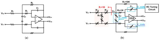
Figure 1.
(a) Conventional MFB filter. (b) The proposed MFB filter with a T-resistor network.
In MFB structures, the Q factor is influenced not only by the gain settings but also by the non-idealities of the OPA, which can deteriorate the actual Q performance further. As pointed out in [17], the non-ideal characteristics of the OPA can lead to an increased Q factor in practical MFB filters, resulting in underdamped frequency responses and degraded in-band flatness. The relationship between the actual Q of the MFB filter () and the finite gain and of the non-ideal OPA is given by [17]
When the filter’s corner frequency is relatively low, remains close to Q. However, as increases, the deviation between and Q becomes more significant. In such cases, a higher gain–bandwidth product is required for the OPA, or, alternatively, a lower Q can be selected to compensate for this effect.
Different gain settings are realized by tuning the ratio between and . However, from the above equations, varying the gain also alters the system’s quality factor Q, impacting both flatness and stability. To address this issue, this paper proposes a T-resistor network, highlighted with the red block in Figure 1b. This approach enables gain adjustment without altering the system’s bandwidth or quality factor. Equally, an RC tuning circuit is adopted, which will be introduced in Section 2.4.
For the subsequent stage, the equivalent resistance of the proposed T-resistor network is given by
The gain of the proposed MFB structure comprises two stages. As the signal flows in, it is first attenuated by the voltage divider formed by and , and then, its gain is adjusted by the MFB core circuit. Therefore, the overall gain of the MFB filter is the product of these two stages. The MFB filter gain with the addition of a T-resistor network is given by
To ensure that gain variations do not affect Q, the proposed T-resistor network’s equivalent resistance value must remain constant throughout the gain adjustment range. Given that and are constant, the gain is only related to . In other words, and must ensure that is constant and that can be changed at the same time to obtain a flexible MFB filter gain.
A set of and values is derived using MATLAB2022 by solving Equations (7) and (8) to achieve a gain adjustment range of 0–19 dB in 1 dB steps while maintaining a constant bandwidth and quality factor. The corresponding resistance values of and for each gain level are listed in Table 1. Additionally, , and .

Table 1.
Equivalent resistance of and in gain control block.
and are implemented as 8-bit binary resistor banks, and the resistor values corresponding to Table 1 are obtained by looking up the table and giving the appropriate codes.
Equally, an MFB filter provides second-order filtering. For higher-order filtering scenarios, multiple MFBs can be cascaded to achieve the desired functionality.
2.2. Nonlinearity Analysis
Since the proposed filter is located at the end of the system chain, it prioritizes linearity and efficiency while ensuring that the noise performance meets the system requirements without incurring excessive power consumption. Figure 2 illustrates the nonlinear output voltage estimation model for the filter. Because the resistor and the capacitor are passive elements, the nonlinearity of the filter is predominantly attributed to the OPA. In multi-stage OPAs, the output stage primarily contributes to distortion because it handles a larger voltage swing compared to that in the pre-stages [18], as shown in Figure 2.
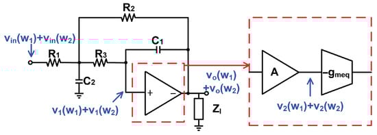
Figure 2.
The nonlinear output voltage estimation model.
As illustrated in Figure 2, the nonlinear behavior of the OPA is modeled using a linear amplifier (A) in combination with a nonlinear equivalent output transconductor , where denotes the effective transconductance of the output-stage NMOS and PMOS transistors, as defined in Equation (9).
It should be noted that as the process corner shifts from fast to typical and finally to slow, the effective decreases, whereas the absolute value of increases. When the circuit is excited by a fixed two-tone input signal (), the input voltage of the output stage is , and the corresponding output voltage of the output stage is . Due to the nonlinear behavior of the output stage, a third-order intermodulation current is injected into the output node, where is the third-order nonlinear coefficient of . Using the model illustrated in Figure 2, we derive the impedance at the output node where the nonlinear current is injected:
Therefore, the nonlinear output voltage at is obtained by multiplying the nonlinear current by the impedance at the output node where the current is injected:
As shown in Equation (13), is inversely proportional to A and while being directly proportional to . Therefore, in order to reduce the component, A and should be increased, while should be reduced.
However, an excessively large A may introduce stability issues, and an overly large would require significant power consumption. Similarly, the value of is constrained by the specific operating region of the transistors. Hence, a reasonable trade-off among stability, power consumption, and linearity must be made.
2.3. The Proposed Operational Amplifier
With growing demand for broadband in modern communication systems, ranging from 20 MHz in LTE to up to 200 MHz in 5G NR, the requirements for broadband low-pass filters have become increasingly stringent. These filters are essential for suppressing out-of-band (OOB) interference, eliminating noise and image signals, and regulating signal strength. As the core component of active low-pass filters, the OPA plays a critical role; its UGB and slew rate directly impact the filter’s frequency response, efficiency, and linearity. Therefore, the design of a high-performance OPA is of paramount importance. Previous studies [13,19,20,21] have introduced feedforward compensation techniques to enhance the phase margin and high-frequency gain. However, since the feedforward transconductance stage () in these designs is placed in the output stage, a large significantly reduces the output resistance, thereby degrading the overall gain. Additionally, the output stage cannot operate in a push–pull manner due to the location of , which compromises the slew rate, linearity, and power efficiency. To address these limitations, this work proposes a three-stage, high-linearity, and high-efficiency current re-use feedforward OPA targeting an enhanced UGB, efficiency, and linearity. Given that the zero introduced by current re-use feedforward compensation is inversely proportional to the feedforward transconductance, this work introduces coupling capacitors to mitigate the adverse impact of the feedforward path on the OPA’s low-frequency performance. Meanwhile, the zero generated by the current re-use feedforward path boosts the high-frequency gain, phase margin, and gain margin further. In addition, an extra Miller zero is introduced to improve the phase margin and the gain margin.
2.3.1. The Design of the Proposed OPA
As illustrated in Figure 3, the proposed OPA consists of an input stage, an inter-stage amplifier, a current re-use feedforward stage, coupling capacitors, a floating bias circuit, a class-AB output stage, and a common-mode feedback error amplifier. The biased circuit of Vbp1, Vbp2, Vbn1, and Vbn2 is omitted for simplicity. To achieve a high loop gain, a three-stage OPA is adopted. The first stage is realized using a telescopic cascode amplifier topology and is self-biased by the large resistors , and small capacitors , . Capacitors and are employed to stabilize the local common-mode loop generated by and . In the second stage, an inverter-based amplifier is used by transistors MN4, MN5, MP6, and MP7 to achieve double . In the last stage, a push–pull output stage is used to achieve a complementary in a large output swing. The output common-mode voltage is regulated by the error amplifier, which feeds back to MP5 in the second stage. The current-re-use feedforward stage with coupling capacitors not only doubles the transconductance to save power but also improves both the low- and high-frequency gain, thereby increasing gain A in Equation (13), which effectively suppresses the nonlinearity of the OPA. Compared to [22], this capacitive coupling reduces the adverse impact of the feedforward path on the low-frequency gain. Furthermore, the current consumption based on current mirrors ensures a robust performance under PVT variations.
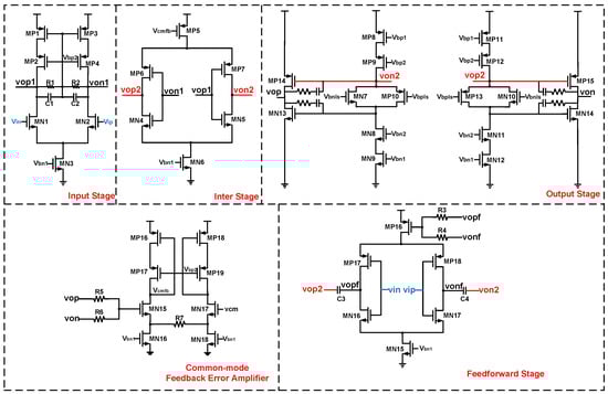
Figure 3.
A schematic of the simplified proposed OPA.
2.3.2. A Stability Analysis
The small-signal model of the proposed OPA is shown in Figure 4. As the frequency increases, the AC-coupling capacitor () gradually acts as a short circuit, allowing the feedforward current to combine with the second-stage current. Although this introduces some deviation in the low-frequency loop gain characteristics, it has a negligible impact on the stability analysis. In this analysis, the coupling capacitor is approximated as a short circuit. For simplification, we assume that the DC gain and the output resistance of each stage are sufficiently large, and all compensation capacitances are significantly larger than the relevant parasitic capacitances but smaller than the load capacitance, as given by
Based on the KCL, the dominant-pole approximation, and the above assumptions, the small-signal open-loop transfer function of the proposed OPA is derived as follows:
where and represent the resistance and capacitance at the node of the Nth output stage, respectively. and represent the transconductance of the Nth stage and the current re-use feedforward stage. is the dominant pole, and is the non-dominant pole, located below the UGB. and are outside of the UGB to ensure the stability of the OPA. generated by RC Miller compensation and generated by the current re-use feedforward stage are located around the UGB to compensate for the phase margin and enhance the high-frequency gain. The locations of the zeros and poles both with the current re-use feedforward technique (WIFF) and without the current re-use feedforward technique (WOFF) are illustrated in Figure 5b. The UGB and phase margin are expressed as
where is the unity-gain bandwidth of the OPA. As can be seen from Equations (13) and (25), increasing at the expense of a higher power consumption can improve the phase margin and reduce the nonlinear output components. Similarly, increasing , also at the cost of a higher power consumption, shifts the zero to a lower frequency, thereby enhancing the phase margin and improving the high-frequency gain, which in turn reduces the nonlinear output components further. can be appropriately reduced to improve the phase margin, with the condition that its noise performance does not affect the overall OPA noise and the driving capability is sufficiently strong. In addition, is mainly determined by the noise requirement, while and are determined by the load, and is determined by the phase margin and the UGB.
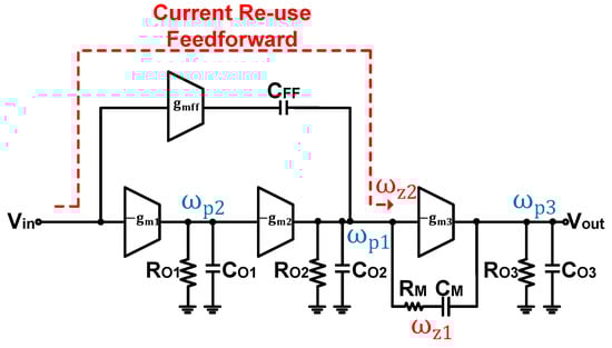
Figure 4.
A small-signal model of the proposed OPA.
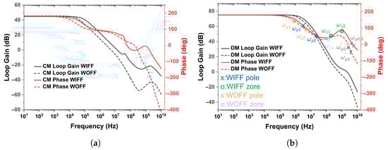
Figure 5.
A comparison of the compensation scheme using Bode plots with a feedback factor of 1/2. (a) A common-mode Bode plot. (b) A differential-mode Bode plot.
According to Equation (23), a large transconductance is required for the zero introduced by the current re-use feedforward path to be located around the UGB, which leads to a high current in the current re-use feedforward stage and subsequently reduces the output impedance. As shown in Equation (17), without the coupling capacitor , would be in parallel with the output resistance of the current re-use feedforward stage, thereby degrading the overall gain . Fortunately, the introduction of not only decouples the output resistance of the current re-use feedforward and second gain stages at low frequencies but also isolates their static currents. This provides greater flexibility to independently adjust the feedforward stage current without impacting the current of the second stage. Furthermore, the feedforward stage adopts a current re-use architecture, combined with a localized common-mode feedback mechanism, which together contribute to improved power efficiency and an enhanced linearity performance. Compared with three-stage OPAs employing two separate feedforward paths [19,23,24], the proposed design utilizes both Miller and current re-use feedforward effects to introduce two zeros more efficiently. This not only reduces the power consumption but also avoids placing the feedforward stage at the output, thereby preserving the linearity and the slew rate. Instead, the proposed OPA employs a push–pull output stage to enhance the linearity and slew rate further.
Figure 5 and Table 2 show simulated differential-mode (DM) and common-mode (CM) Bode plots of the proposed WIFF OPA and a conventional WOFF OPA in a unity-gain inverting feedback structure, where the feedback factor () is 0.5. The proposed OPA demonstrates a substantial improvement in the high-frequency gain and UGB while maintaining a similar power consumption and phase margin. Compared to conventional OPAs, this improvement highlights the effectiveness of the proposed OPA based on current re-use feedforward and Miller compensation. At similar phase margins for both structures, the loop gain at 100 MHz, the BW, and the UGB for the WIFF structure are 28.75 dB, 2.14 MHz, and 2.14 GHz, respectively, compared to only 22.34 dB, 1.33 MHz, and 0.61 GHz for the conventional WOFF structure.
Table 2.
Simulation results of the compared compensation technique.
2.4. The RC Tuning Circuit
From the derivation in Section 2, the filter bandwidth . It can be seen that the bandwidth of the filter is closely related to the resistance and capacitance in the circuit. However, variations in the PVT cause deviations in resistance and capacitance, leading to bandwidth fluctuations that impact system performance. To maintain bandwidth stability, an RC tuning circuit is required to compensate for variations in the RC time constant. The RC tuning circuit, shown in Figure 6a, consists of four components:
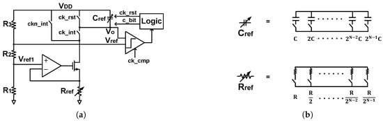
Figure 6.
(a) RC tuning circuit. (b) Resistor bank and capacitor bank in RC tuning circuit.
(1) An integration circuit: This facilitates charging and discharging of the capacitor bank to measure the RC time constant. (2) A clock circuit: This generates the required RC tuning clock, integration clock, and comparator sampling clock from an external input clock. A specific schematic of the clock generation circuit is shown in Figure 7. First, two D latches connected in positive feedback halve the input clock CLK frequency and convert it into four-phase signals with a 50% duty cycle: P1, P2, P3, and P4. Then, by combining inverters and logic gates, the required clock signals ck_rst, ck_int, and ck_cmp are obtained. The timing sequence is shown in Figure 8b. (3) A comparator: This detects the integration voltage to determine whether the RC tuning has reached the target time constant. As shown in Figure 8a, a double-tail comparator is employed in this work. The double-tail comparator exhibits minimal delay, enabling completion of the comparison within ck_cmp without affecting subsequent integration cycles in ck_int. (4) Digital logic control: This adjusts the RC tuning input according to the output of the comparator.

Figure 7.
RC tuning clock circuit.

Figure 8.
(a) Comparator circuit. (b) RC tuning timing diagram.
The basic principle of RC tuning is based on the charge and discharge characteristics of the integral circuit. The timing diagram is shown in Figure 8b. During each tuning cycle, ck_rst is enabled first, driving to to establish the initial state. The high-gain amplifier forces the voltage across at , ensuring a constant current. Then, ck_rst is disabled and ck_int is enabled; integration begins charging and follows the equation below:
The integration time remains constant. Once the integration is complete, ck_int is disabled, ck_cmp is enabled, and the comparator starts to check whether reaches . If not, the capacitor bank code adds one and repeats the above process until the comparator output transitions. Multiple comparisons are made between the codes at which the comparator output transitions, and the most suitable code is chosen as the final output.
Upon the completion of tuning, the tuning circuit automatically shuts down to reduce the power consumption and prevent interference with the signal path. After tuning, the system satisfies the following equation:
Combining Equations (26) and (27) gives
From Equation (28), it follows that after tuning, remains constant and is only related to .To enable RC time constant tuning across different bandwidths, is implemented as a resistor bank. The capacitor bank and the resistor bank used in the tuning circuit are illustrated in Figure 6b.
3. Post-Simulation Results
The proposed MFB filter has been designed using 28 nm CMOS technology. The layout of the MFB filter with the RC tuning circuit is shown in Figure 9. The areas of the MFB filter and the RC tuning circuit are 0.036 mm2 and 0.02 mm2, respectively. Under process corners and supply voltage variations at , the MFB filter exhibits an average power consumption ranging from to , with a standard deviation of to . The RC tuning circuit shows an average power consumption between and , with a standard deviation of to . At the typical TT corner at , the power consumption of the MFB filter is , which excludes the contribution of the RC tuning circuit.
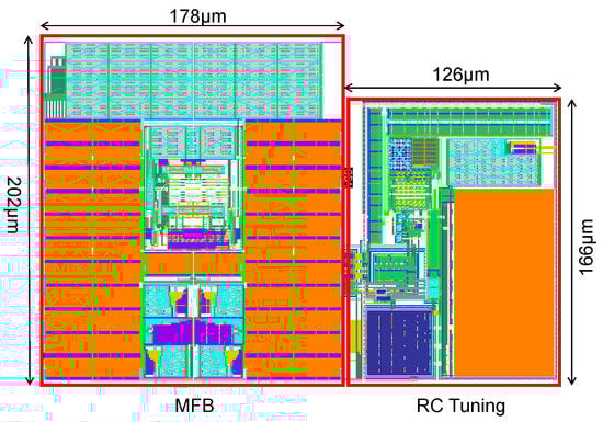
Figure 9.
Layout of 2nd-order MFB filter with RC tuning circuit.
Post-simulation results for the proposed circuits are obtained with the aid of Cadence Virtuoso. As shown in Figure 10a, the proposed structure maintains a constant Q, whereas in the conventional MFB filter, Q and BW vary with the gain, as depicted in Figure 10b, which can further adversely affect the in-band (IB) flatness, the error vector magnitude (EVM), and the adjacent channel leakage ratio (ACLR). Figure 10b is simulated in Figure 1a’s structure, using the same bandwidth and gain settings as those in Figure 1b. Figure 11 shows the frequency responses of the MFB filter under PVT variations before and after tuning in the 10 MHz bandwidth. It can be observed that the bandwidths of the MFB filter are all closer after tuning under PVT variations. The bandwidths before and after tuning, along with the tuning error, are shown in Table 3. The proposed approach allows for independent adjustment of the bandwidth and gain, as illustrated in Figure 12a.

Figure 10.
(a) Proposed gain control in MFB filter. (b) Conventional gain control in MFB filter.
Figure 11.
(a) A 10 MHz bandwidth without tuning. (b) A 10 MHz bandwidth with tuning.
Table 3.
Bandwidth under PVT variations.
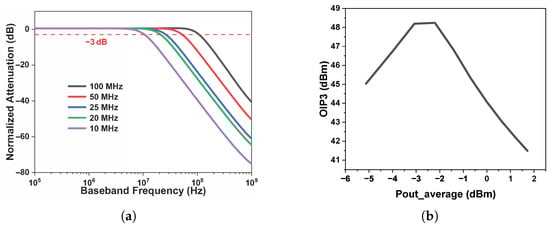
Figure 12.
(a) Proposed programmable bandwidth in MFB filter. (b) OIP3 versus average output power for two-tone signals at 92 MHz and 100 MHz.
To evaluate the performance under the most demanding conditions, the bandwidth of the MFB filter is configured to its maximum value of 100 MHz. The OIP3 at the band edge, with input frequencies of 92 MHz and 100 MHz, is shown in Figure 12b, and it remains above 41.5 dBm across different output power levels. The IB and OOB two-tone intermodulation post-simulation results are shown in Figure 13a. For the IB OIP3, the two-tone space is 1 MHz. The first tone changes from 10 MHz to 90 MHz, and the IB OIP3 changes from 48.2 dBm to 47.7 dBm. For the OOB OIP3, is fixed at 1 MHz. As the first tone sweeps from 110 MHz to 170 MHz, the OOB OIP3 increases from 48.8 dBm to 53.4 dBm. Figure 13c shows that the IB OIP3 is 48.2 dBm when the two-tone frequencies are 10 MHz and 11 MHz, and the OOB OIP3 is 53.4 dBm when the two-tone frequencies are 170 MHz and 339 MHz. The spectrum when two-tone frequencies of 10 MHz and 11 MHz are applied is shown in Figure 13d, demonstrating an output power of −1.7 dBm and an IM3 of −101.5 dBm. So, this filter can achieve high linearity with 3.6 mW of power consumption (). The post-simulation 1 dB compression point (P1dB) is 15.5 dBm, as shown in Figure 14a. The IB integrated noise is 147 () from 1 MHz to 100 MHz. The equivalent IB spectral noise density is 14.8 , as shown in Figure 14b. The CM and DM phase margins are shown in Table 4, where the CM phase margin exceeds 47° and the DM phase margin exceeds 40°. In order to evaluate the stability and performance of the MFB filter based on the proposed OPA, Monte Carlo (MC) simulations are conducted, and histograms are shown for the , DC gain, phase margin, and gain margin in Figure 15. Figure 16a illustrates the step response of the proposed OPA in the MFB filter when the phase margin is . With large-signal excitation (a input step), the circuit exhibits a overshoot, indicating stable operation. Since the MFB is a continuous-time filter, the resulting ripple does not have a significant impact on the performance.

Figure 13.
(a) OIP3 vs. first-tone frequency (). (b) OIP3 vs. IM3 frequency. (c) OIP3 with two-tone frequencies at 10 MHz and 11 MHz and 170 MHz and 339 MHz. (d) Spectrum with two-tone frequencies at 10 MHz and 11 MHz.
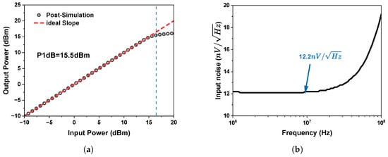
Figure 14.
(a) P1dB with single tone at 10 MHz. (b) Input-referred noise density of MFB filter.
Table 4.
Phase margin in corners.
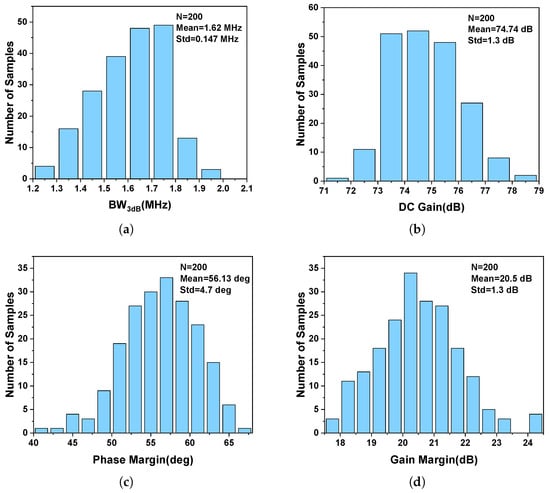
Figure 15.
MC histograms. (a) . (b) DC gain. (c) Phase margin. (d) Gain margin.
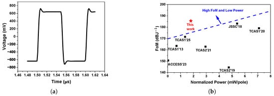
Figure 16.
(a) The simulated step response of the proposed OPA in MFB for an input signal (1.28-Vpp). (b) FoM versus normalized power.
Moreover, the post-simulation results are discussed and compared with the state-of-the-art in active filters in Table 5. The proposed MFB filter achieves a wider bandwidth, a lower power, and the highest linearity compared to [18,22,25,26]. This work and [11] are both wideband filters, while the SFDR and IB OIP3 in this work are better. Compared to the work [27], this work demonstrates a slightly improved power consumption and linearity, along with a notably wider bandwidth. The noise performance of this work is less prominent than that in some recent works because the proposed filter operates in the back-end of the system chain, where linearity is more critical than noise. Since improving noise usually requires a much higher power consumption, we adopt a reasonable trade-off between noise and efficiency. It is worth noting that this work achieves the highest linearity and figure-of-merit (FoM) in the table. Typically, Fom and power consumption are positively correlated. As shown in Figure 16b, this work breaks this relationship and achieves a better FoM with a lower power consumption.
Table 5.
Comparison with state-of-the-art works.
4. Conclusions
Wideband Active-RC filters are commonly used in the baseband of wireless transceivers. In this work, we propose a novel MFB filter with a reconfigurable bandwidth and gain, supporting up to a 100 MHz bandwidth. Unlike conventional MFB filters, where the gain and quality factor are difficult to decouple, the proposed design allows for independent adjustment of the bandwidth and gain without affecting the quality factor. This method makes the MFB filter behave like a Tow–Thomas filter in terms of flexible gain and bandwidth tuning while retaining the advantage of using only one operational amplifier, significantly reducing the power consumption and area, and thereby broadening its application scenarios. The bandwidth is tunable from 10 MHz to 100 MHz, while the gain can be adjusted from 0 dB to 19 dB with a 1 dB gain step. Additionally, a three-stage OPA with current re-use feedforward and RC Miller compensation is proposed to achieve high efficiency and linearity. RC tuning is implemented to maintain a stable bandwidth across PVT variations. The proposed MFB filter achieves an IB OIP3 of 48.2 dBm and an OOB OIP3 of 53.4 dBm, along with a FoM of 185.5 dBJ−1, while consuming only 3.6 mW of power under a 100 MHz bandwidth configuration. Notably, the proposed MFB filter achieves the highest FoM compared to that in prior works, highlighting its superior linearity and power efficiency.
Author Contributions
Conceptualization: M.J. and T.X.; methodology: M.J. and T.X.; software: M.J. and T.X.; validation: M.J. and T.X.; formal analysis: M.J. and T.X.; investigation: M.J. and T.X.; resources: M.J. and T.X.; data curation: M.J. and T.X.; writing—original draft preparation: M.J. and T.X.; writing—review and editing: M.J., T.X. and Y.C.; visualization: M.J. and T.X.; supervision: M.J. and T.X.; project administration: J.W. and Y.C.; funding acquisition: J.W. All authors have read and agreed to the published version of the manuscript.
Funding
This research was funded by a National Natural Science Foundation of China Project, grant number 62090044.
Data Availability Statement
The data are contained within the article.
Conflicts of Interest
The authors declare no conflicts of interest.
References
- 3GPP. NR; Base Station (BS) Radio Transmission and Reception, 3GPP TS 38.104, Version 18.5.0. 3rd Generation Partnership Project (3GPP). 2024. Available online: https://www.3gpp.org/dynareport/38104.htm (accessed on 31 August 2025).
- Tsividis, Y. Integrated Continuous-Time Filter Design. In Proceedings of the IEEE Custom Integrated Circuits Conference—CICC’93, San Diego, CA, USA, 9–12 May 1993. [Google Scholar] [CrossRef]
- Houfaf, F.; Egot, M.; Kaiser, A.; Cathelin, A.; Nauta, B. A 65nm CMOS 1-to-10GHz Tunable Continuous-Time Low-Pass Filter for High-Data-Rate Communications. In Proceedings of the 2012 IEEE International Solid-State Circuits Conference, San Francisco, CA, USA, 19–23 February 2012; pp. 362–364. [Google Scholar] [CrossRef]
- Algueta-Miguel, J.M.; De La Cruz Blas, C.A.; Lopez-Martin, A.J. Balanced Gm-C Filters with Improved Linearity and Power Efficiency. Int. J. Circuit Theory Appl. 2015, 43, 1147–1166. [Google Scholar] [CrossRef]
- Algueta-Miguel, J.M.; De la Cruz Blas, C.A.; Lopez-Martin, A.J. A 760μW 4th Order Butterworth FGMOS Gm-C Filter with Enhanced Linearity. In Proceedings of the 2015 IEEE International Symposium on Circuits and Systems (ISCAS), Lisbon, Portugal, 24–27 May 2015; pp. 277–280. [Google Scholar] [CrossRef]
- Le-Thai, H.; Nguyen, H.H.; Nguyen, H.N.; Cho, H.S.; Lee, J.S.; Lee, S.G. An IF Bandpass Filter Based on a Low Distortion Transconductor. IEEE J. Solid-State Circuits 2010, 45, 2250–2261. [Google Scholar] [CrossRef]
- Kim, J.; Lee, Y.; Chang, S.; Shin, H. Low-Power CMOS Complex Bandpass Filter with Passband Flatness Tunability. Electronics 2020, 9, 494. [Google Scholar] [CrossRef]
- De Matteis, M.; Pipino, A.; Resta, F.; Pezzotta, A.; D’Amico, S.; Baschirotto, A. A 63-dB DR 22.5-MHz 21.5-dBm IIP3 Fourth-Order FLFB Analog Filter. IEEE J. Solid-State Circuits 2017, 52, 1977–1986. [Google Scholar] [CrossRef]
- Wang, Y.; Ye, L.; Liao, H.; Huang, R.; Wang, Y. Highly Reconfigurable Analog Baseband for Multistandard Wireless Receivers in 65-nm CMOS. IEEE Trans. Circuits Syst. II Express Briefs 2015, 62, 296–300. [Google Scholar] [CrossRef]
- Wang, Y.; Wu, B.; Huang, H. A 3rd/5th Order Active RC Chebyshev Analog Baseband Low-Pass Filter with Reconfigurable Bandwidth and Gain. IEEE Access 2021, 9, 129319–129328. [Google Scholar] [CrossRef]
- Ye, L.; Shi, C.; Liao, H.; Huang, R.; Wang, Y. Highly Power-Efficient Active-RC Filters with Wide Bandwidth-Range Using Low-Gain Push-Pull Opamps. IEEE Trans. Circuits Syst. I Regul. Pap. 2013, 60, 95–107. [Google Scholar] [CrossRef]
- Zhan, J.H.C.; Carlton, B.R.; Taylor, S.S. A Broadband Low-Cost Direct-Conversion Receiver Front-End in 90 nm CMOS. IEEE J. Solid-State Circuits 2008, 43, 1132–1137. [Google Scholar] [CrossRef]
- Thandri, B.; Silva-Martinez, J. A Robust Feedforward Compensation Scheme for Multistage Operational Transconductance Amplifiers with NO Miller Capacitors. IEEE J. Solid-State Circuits 2003, 38, 237–243. [Google Scholar] [CrossRef]
- Rasekh, A.; Sharif Bakhtiar, M. Design of Low-Power Low-Area Tunable Active RC Filters. IEEE Trans. Circuits Syst. II Express Briefs 2018, 65, 6–10. [Google Scholar] [CrossRef]
- Cao, W.; Gao, J.; Ma, T.; Ma, R.; Benosman, M.; Zhang, X. RoSE-Opt: Robust and Efficient Analog Circuit Parameter Optimization With Knowledge-Infused Reinforcement Learning. IEEE Trans. Comput.-Aided Des. Integr. Circuits Syst. 2025, 44, 627–640. [Google Scholar] [CrossRef]
- Tang, C.C.; Lee, Y.B.; Sun, C.H.E.; Lin, C.C.; Syu, J.S.; Wu, M.H.; Chen, Y.; Chueh, T.C.; Bryant, C.; Collados, M.; et al. 21.4 An LTE-A Multimode Multiband RF Transceiver with 4RX/2TX Inter-Band Carrier Aggregation, 2-Carrier 4×4 MIMO with 256QAM and HPUE Capability in 28nm CMOS. In Proceedings of the 2019 IEEE International Solid-State Circuits Conference—(ISSCC), San Francisco, CA, USA, 17–21 February 2019; pp. 350–352. [Google Scholar] [CrossRef]
- Thomas, L. The Biquad: Part I-Some Practical Design Considerations. IEEE Trans. Circuit Theory 1971, 18, 350–357. [Google Scholar] [CrossRef]
- Lei, L.; Tao, C.; Chen, Z.; Hong, Z.; Huang, Y. A Power-Efficient Active-RC Filter Using Passive Integrator and OTA with Push-Pull Output. IEEE Trans. Circuits Syst. I Regul. Pap. 2025, 1–11. [Google Scholar] [CrossRef]
- Harrison, J.; Weste, N. A 500 MHz CMOS Anti-Alias Filter Using Feed-Forward Op-Amps with Local Common-Mode Feedback. In Proceedings of the 2003 IEEE International Solid-State Circuits Conference, 2003, Digest of Technical Papers, ISSCC, San Francisco, CA, USA, 13 February 2003; Volume 1, pp. 132–483. [Google Scholar] [CrossRef]
- Zhou, D.; Briseno-Vidrios, C.; Jiang, J.; Park, C.; Liu, Q.; Soenen, E.G.; Kinyua, M.; Silva-Martinez, J. A 13-Bit 260MS/s Power-Efficient Pipeline ADC Using a Current-Reuse Technique and Interstage Gain and Nonlinearity Errors Calibration. IEEE Trans. Circuits Syst. I Regul. Pap. 2019, 66, 3373–3383. [Google Scholar] [CrossRef]
- Yun, S.; Cho, C.; Jo, S.; Kwon, K. A 2.7-dB NF 55-dBm IIP2 Blocker-Tolerant Receiver Front End Employing Dual RF and BB N-Path Filters for 5G New Radio Cellular Applications. IEEE Trans. Microw. Theory Tech. 2025, 73, 1558–1572. [Google Scholar] [CrossRef]
- Jung, H.; Utomo, D.R.; Han, S.K.; Kim, J.; Lee, S.G. An 80 MHz Bandwidth and 26.8 dBm OOB IIP3 Transimpedance Amplifier With Improved Nested Feedforward Compensation and Multi-Order Filtering. IEEE Trans. Circuits Syst. I Regul. Pap. 2020, 67, 3410–3421. [Google Scholar] [CrossRef]
- Hu, Y.; Liu, Y.; Qin, X.; Liu, Y.; Guo, M.; Sin, S.W.; Wang, G.; Lian, Y.; Qi, L. A Two-Channel Time-Interleaved Continuous-Time Third-Order CIFF-Based Delta-Sigma Modulator. IEEE Trans. Circuits Syst. I Regul. Pap. 2023, 70, 4729–4741. [Google Scholar] [CrossRef]
- Wu, B.; Chiu, Y. A 40 nm CMOS Derivative-Free IF Active-RC BPF With Programmable Bandwidth and Center Frequency Achieving Over 30 dBm IIP3. IEEE J. Solid-State Circuits 2015, 50, 1772–1784. [Google Scholar] [CrossRef]
- Lim, J.; Kim, J. A 20-kHz 16-MHz Programmable-Bandwidth 4th Order Active Filter Using Gain-Boosted Opamp With Negative Resistance in 65-nm CMOS. IEEE Trans. Circuits Syst. II Express Briefs 2019, 66, 182–186. [Google Scholar] [CrossRef]
- Park, C.; Tavares, Y.A.; Lee, J.; Wo, J.; Lee, M. 5th-Order Continuous-Time Low-Pass Filter Achieving 56 MHz Bandwidth 30.5 dBm IIP3 With a Novel Low-Distortion Amplifier. IEEE Trans. Circuits Syst. II Express Briefs 2021, 68, 1768–1772. [Google Scholar] [CrossRef]
- Pini, G.; Manstretta, D.; Castello, R. Analysis and Design of a 20-MHz Bandwidth, 50.5-dBm OOB-IIP3, and 5.4-mW TIA for SAW-Less Receivers. IEEE J. Solid-State Circuits 2018, 53, 1468–1480. [Google Scholar] [CrossRef]
- Ghasemi, A.R.; Aminzadeh, H.; Ballo, A. Ladder-Type Gm-C Filters With Improved Linearity. IEEE Access 2023, 11, 41503–41513. [Google Scholar] [CrossRef]


Disclaimer/Publisher’s Note: The statements, opinions and data contained in all publications are solely those of the individual author(s) and contributor(s) and not of MDPI and/or the editor(s). MDPI and/or the editor(s) disclaim responsibility for any injury to people or property resulting from any ideas, methods, instructions or products referred to in the content. |
© 2025 by the authors. Licensee MDPI, Basel, Switzerland. This article is an open access article distributed under the terms and conditions of the Creative Commons Attribution (CC BY) license (https://creativecommons.org/licenses/by/4.0/).