Article

A Modulated Marx Generator Capable of Outputting Quasi-Square Waves

1
College of Advanced Interdisciplinary Studies, National University of Defense Technology, Changsha 410073, China
2
State Key Laboratory of Pulsed Power Laser Technology, Changsha 410073, China
*
Author to whom correspondence should be addressed.
Electronics 2025, 14(17), 3517; https://doi.org/10.3390/electronics14173517
Submission received: 13 August 2025 / Revised: 28 August 2025 / Accepted: 29 August 2025 / Published: 2 September 2025
(This article belongs to the Section Power Electronics)

Abstract

A pulse generator capable of outputting quasi-square-wave pulses at the hundred-nanosecond scale is designed. With the development of high-power microwaves, the pulse flat-top is required to be more and more stable. However, at the hundred-nanosecond scale, an equal-value pulse-forming network is prone to being affected by stray parameters in the output waveform. To meet this requirement, a Marx generator and an anti-resonant network is used as the pulse boosting component and the pulse modulation component, respectively. Taking advantage of the anti-resonant network’s fewer sections and good modulation effect, the output waveform of the Marx generator is improved. The modulation ability of two-section and three-section modulation networks on waveforms, the output characteristics of two-section modulation networks, and the effect of stray parameters on the modulation network are explored. The experimental results show that both networks were able to achieve a quasi-square waveform of 100 kV on a 50 Ω load. Compared to the two-section network (165 ns pulse width, 41 ns rise time, 54.54% waveform flatness), the proposed three-section network achieves a pulse width of 185 ns with faster rise time (25 ns) and better waveform flatness (63.78%). Both topologies generate 100 kV quasi-square pulses on 50 Ω loads, with the three-section design demonstrating superior waveform control. In the repetition experiment, the pulse power source achieved stable operation at a repetition frequency of 20 Hz, and a quasi-square waveform with an output voltage of 100 kV was obtained. Finally, compared with previous studies, the modulated Marx generator based on an anti-resonant network has better waveform modulation effect and fewer network sections when generating a Square wave pulse of 100–200 ns.

1. Introduction

Pulse power technology, as a key supporting technology in the field of high-energy physics, has been widely applied in various areas such as defense technology, industrial manufacturing, and environmental protection. Typical application scenarios include high-power microwave (HPM) systems, inertial confinement fusion, and industrial waste gas treatment [1,2,3]. Particularly in HPM systems, the pulse flat-top design of the pulse power source is a critical technical requirement. The flat-top characteristics of the pulse directly affect system performance, and its core role can be reflected in the following two aspects: ➀ enhancing energy conversion efficiency by suppressing interference from reflected waves [4]; and ➁ maintaining the stability of the electron beam, providing stable operating conditions for microwave generation [5]. Furthermore, the pulse width of the majority of narrowband GW and sub-GW class HPM systems ranges from 20 to 200 ns [6,7,8,9,10,11,12,13,14,15,16,17,18,19], which is limited by both physical mechanisms and application requirements. An excessively long pulse width can lead to detrimental effects, such as the potential burnout of the microwave tube and the occurrence of pulse shortening [20,21,22,23,24,25,26,27,28,29]. Moreover, the pulse width of HPM should not be excessively short; in electronic countermeasures, the effectiveness of HPM against autonomous aerial vehicles is directly proportional to the pulse width [30]. According to the current application requirements for HPM [31], the development trend of pulse power sources is to generate higher-quality high-voltage square-wave pulses.
With the rapid development of switching devices and compact pulse power technology, the Marx generator, with its modular topology and cascading voltage boosting characteristics, has been widely used in the design of pulse power source [32,33,34,35]. The modulated Marx generator is a pulse power source that combines the voltage boosting function of the Marx generator with the waveform modulation function of a pulse-forming network (PFN). The PFN–Marx generator, based on equal capacitance and equal inductance pulse-forming networks, is the most common type that can output square waves [36]. The PFN–Marx generator simulates transmission line characteristics through an LC network to output square waves. However, this simulated transmission line requires a large number of LC units to produce sufficiently good pulse square waves [37]. This not only increases the size of the PFN–Marx generator but also makes it very susceptible to the influence of parasitic parameters [38]. Therefore, an equal inductance and equal capacitance network is more suitable for outputting a long pulse width, as the impact of parasitic parameters becomes more pronounced when the pulse width shortens. Additionally, considering the manufacturing tolerances of inductors and capacitors, these factors limit the PFN–Marx generator’s ability to output higher-quality square waveforms.
An anti-resonant network is a type of PFN with unequal component parameters. Unlike a PFN, based on the principle of simulated transmission lines with equal capacitance and inductance, an anti-resonant network is designed using the Fourier frequency analysis method. Due to its characteristic of having unequal component parameters, this network can achieve the effect of square-wave modulation with fewer network sections, making it easier to compact and stabilize the pulse modulation unit [39]. Currently, anti-resonant networks have been experimentally studied in some pulse devices, such as the Fractional Ratio Saturable Pulse Transformer [40] and the Transmission Line Transformer [41]. Experimental results indicate that anti-resonant networks demonstrate good waveform modulation effects in microsecond and sub-microsecond pulses. Due to their fewer network sections, they are more suitable for outputting high-quality waveforms of short pulse width compared to equal capacitance and equal inductance networks.
Due to the characteristic of anti-resonant networks requiring only a few network sections (2–3 sections) to modulate square-wave pulses, they are less affected by parasitic parameters. As a result, within the pulse range of 100–200 ns, compared to the equivalent PFN, an anti-resonant network can produce pulses with better waveform flatness. This meets the high-power microwave demand for improved pulse waveform quality. Meanwhile, the Marx generator, as a capacitor energy storage-based voltage boosting device, has the potential to be combined with an anti-resonant network, making the implementation of a modulated Marx generator based on an anti-resonant network possible.
A short pulse modulated Marx generator based on an anti-resonant network is proposed and designed in this paper. The system consists of three parts: primary energy, pulse boosting, and pulse modulation. The Marx generator is mainly used for pulse boosting. To accommodate applications in the hundreds of kV range, a gas spark gap is used as the working switch for the Marx generator. The anti-resonant network is the core of pulse modulation to achieve high-quality square-wave pulses. The main contributions are summarized as follows.
  • A modulated Marx generator capable of outputting square-wave short pulses is proposed based on an anti-resonant network.
  • The circuit characteristics of the modulated Marx generator designed in this paper are studied, including the modulation effect of the anti-resonant network, the output characteristics of the system and the influence of stray parameters on the system.
  • Experiments are conducted on the modulated Marx generator designed in this paper, including single experiments and repetition experiments. The quality and stability of the waveforms are analyzed, and the energy efficiency of the modulated Marx generator is calculated.
In order to better reflect the research value of this paper, the metrics of the pulse waveform are quantified. The usual metrics of pulse are pulse width (full width at half maximum), leading edge, trailing edge, etc. The schematic diagram of the metrics is shown in Figure 1. On this basis, this paper introduces waveform flatness γ, which is used to measure the flatness of the pulse flat-top. It can be calculated from Equation (1).
γ = t f τ o
In the above equation, t f is the duration of 90% of the peak voltage, which can also be defined by 80% of the peak voltage. τ o is the pulse width of the pulse. The larger the waveform flatness γ, the better the flatness of the pulse waveform.
Chapter 2 provides a detailed introduction to the design of a modulated Marx generator based on an anti-resonant network. Chapter 3 presents the experimental results of the output waveforms of the pulse power source (including single experiment and repetition experiment), then compares and analyzes the modulation effects of different numbers of sections of the anti-resonant network in the Marx generator. Finally, Chapter 4 compares some other PFN–Marx generators for high-power microwave applications and summarizes the design of this paper.

2. Design of Modulated Marx Generator

2.1. Overview of the Modulated Marx Generator

This part introduces the system composition of the modulated Marx generator, with the system schematic shown in Figure 2. The pulse power source consists of a rectifier circuit, pulse air-core transformer, Marx generator, anti-resonant network, triggering system, and load. The rectifier circuit and the pulse air-core transformer serve as the primary energy for the system, charging the capacitors in the Marx generator. The Marx generator acts as the core pulse boosting component, and the waveform is modulated through the anti-resonant network. The triggering system is used to trigger the first switch of the Marx generator.
The workflow of the entire system is as follows: The AC 220 V is first rectified and stepped up by the rectifier circuit and the pulse air-core transformer, charging the capacitors in the Marx generator. Once the Marx generator is fully charged, the triggering system activates the first switch of the Marx generator, causing the next switch to turn on, and this continues until all switches are activated, resulting in voltage addition. The voltage waveform directly output by the Marx generator is an exponentially decaying triangular wave, which is modulated by the anti-resonant network to form a quasi-square wave, ultimately releasing it to the load.

2.2. The Structure of the Marx Generator

The Marx generator is the core boosting component in the system. Its principle is to achieve high-voltage pulse output by charging capacitors in parallel and then discharging them in series. The circuit diagram of the Marx generator is shown in Figure 3.
The designed Marx generator has 12 stages, with a load resistance of 50 Ω. To improve the charging efficiency and operational stability of the pulse power source, a bipolar charging method is used, which reduces the number of switches by half. The energy storage capacitors used are 17.5 nF/50 kV film capacitors, with dimensions of 211 mm × 62 mm × 153 mm. To enhance the repetition frequency operation capability and energy efficiency of the pulse power source, an inductor is used as an isolation component during the charging of the energy storage capacitors, with an inductance value of approximately 35 μH for each stage.
The Marx generator in this paper adopts a compact design method, dividing the 12 energy storage capacitors into two groups, arranged in an insulating framework that serves both insulation and support functions. Additionally, 4 modulation capacitors are also placed within the insulating framework. All switches are arranged in a single row, which facilitates synchronous triggering of the switches [42]. The entire Marx generator is housed in a sealed aluminum cylinder, allowing for the filling of insulating gas inside the cylinder to enhance the system’s insulation capability. The structure diagram of the designed modulated Marx generator is shown in Figure 4.

2.3. Pulse Square Wave Modulator

The core of pulse modulation is the anti-resonant network, which consists of multiple sections of resonant networks. Generally, an N-section anti-resonant network is composed of a series LC resonant network and N-1 parallel LC resonant networks. The circuit diagram is shown in Figure 5:
Due to the presence of a series LC resonant network in the structure of the anti-resonant network, and the fact that the Marx generator can be equivalently represented as an LCR series discharge during the discharge process, the anti-resonant network can be well combined with the Marx generator. In the specific design, it just needs to cascade N-1 sections of LC parallel resonant networks after the Marx generator to form an N-section anti-resonant network. The values of C1 and L1 are mainly determined by the Marx generator, and only the remaining N-1 sections of the LC parallel resonant network need to be designed to achieve the effect of pulse shaping.
A square-wave pulse can be expressed using a Fourier series expansion with variable coefficients. Since the Guillemin network is constructed from the Fourier series of a periodic square wave, the output voltage expression of the anti-resonant network based on the Guillemin type-A network can be expanded into a Fourier series with variable coefficients. The number of terms in the Fourier series corresponds to the number of sections in the anti-resonant network. According to Figure 5, the circuit’s KCL and KVL equations can be established. By applying the Laplace transform, the Laplace transform expression of the current on the load can be solved. Then, by matching this with the Laplace transform of the Fourier series expansion with variable coefficients, the parameters of each component in the anti-resonant network can be determined.
Previous studies have shown that the more sections an anti-resonant network has, the better the waveform modulation effect [43]. However, to avoid the increase in stray parameter effects caused by too many sections in the network, an anti-resonant network with no more than three sections is chosen as the pulse-forming network for the modulated Marx generator. This can meet the dual requirements of pulse modulation and compactness. Specifically, experiments are conducted on both a two-section anti-resonant network and a three-section anti-resonant network. The parameters for the two-section anti-resonant network can be determined by Equation (2), while the parameters for the three-section anti-resonant network can be determined by Equation (3).
C 1 = 0.420 τ ρ L 1 = 0.328 τ ρ C 2 = 0.315 τ ρ L 2 = 0.057 τ ρ
C 1 = 0.435 τ ρ L 1 = 0.2201 τ ρ C 2 = 0.450 τ ρ L 2 = 0.0121 τ ρ C 3 = 0.250 τ ρ L 3 = 0.0838 τ ρ
In the above equation, τ is the pulse width (in ns), ρ is the load resistance (in Ω), C1 and L1 are the capacitance and inductance values in the series resonant circuit, C2 and L2 are the capacitance and inductance values in the first parallel resonant circuit, and C3 and L3 are the capacitance and inductance values in the second parallel resonant circuit.

2.4. Simulation of Complete Circuits

Using PSpice to establish a circuit simulation model, the main purpose is to verify the modulation effect of the anti-resonant network on the output waveform of the Marx generator. The designed Marx generator is a 12-stage bipolar charging and isolated by inductance, with each stage capacitor at 17.5 nF, an ideal pulse width of 150 ns, and a load of 50 Ω. Based on the capacitance, pulse width, load, and Equations (1) and (2), the parameters of the anti-resonant network can be calculated, with the specific results as follows:
C 1 1.458   n F L 1 = 2460   n H C 2 = 0.945   n F L 2 = 427.5   n H
C 1 1.458   n F L 1 = 1650.75   n H C 2 = 1.35   n F L 2 = 90.75   n H C 3 = 0.75   n F L 3 = 628.5   n H
The simulation solver and switch settings are shown in Table 1 below. Unless otherwise specified, all simulations are conducted using the following settings.
The load voltage of the two types of Marx generators is shown in Figure 6. With a load of 50 Ω, the pulse width of the output voltage from the two-section anti-resonant network is approximately 170 ns, while the pulse width from the three-section anti-resonant network is about 150 ns. From the perspective of waveform quality, the three-stage anti-resonant network has a faster rise time, a longer flat-top duration, and a pulse width that is closer to the design value compared to the two-section anti-resonant network. However, the three-stage anti-resonant network increases the size and complexity of the system. Overall, both types of networks basically meet the design requirements.

2.5. Output Characteristics of Anti-Resonant Networks

An anti-resonant network is a pulse-forming network with unequal parameters. The component parameters calculated by Equations (2) and (3) are often difficult to fabricate precisely. Additionally, due to manufacturing tolerances in capacitance and inductance, some approximation is necessary in practice. To achieve acceptable accuracy, the influence of the parameters of different components in the anti-resonant network on the output characteristics is analyzed.
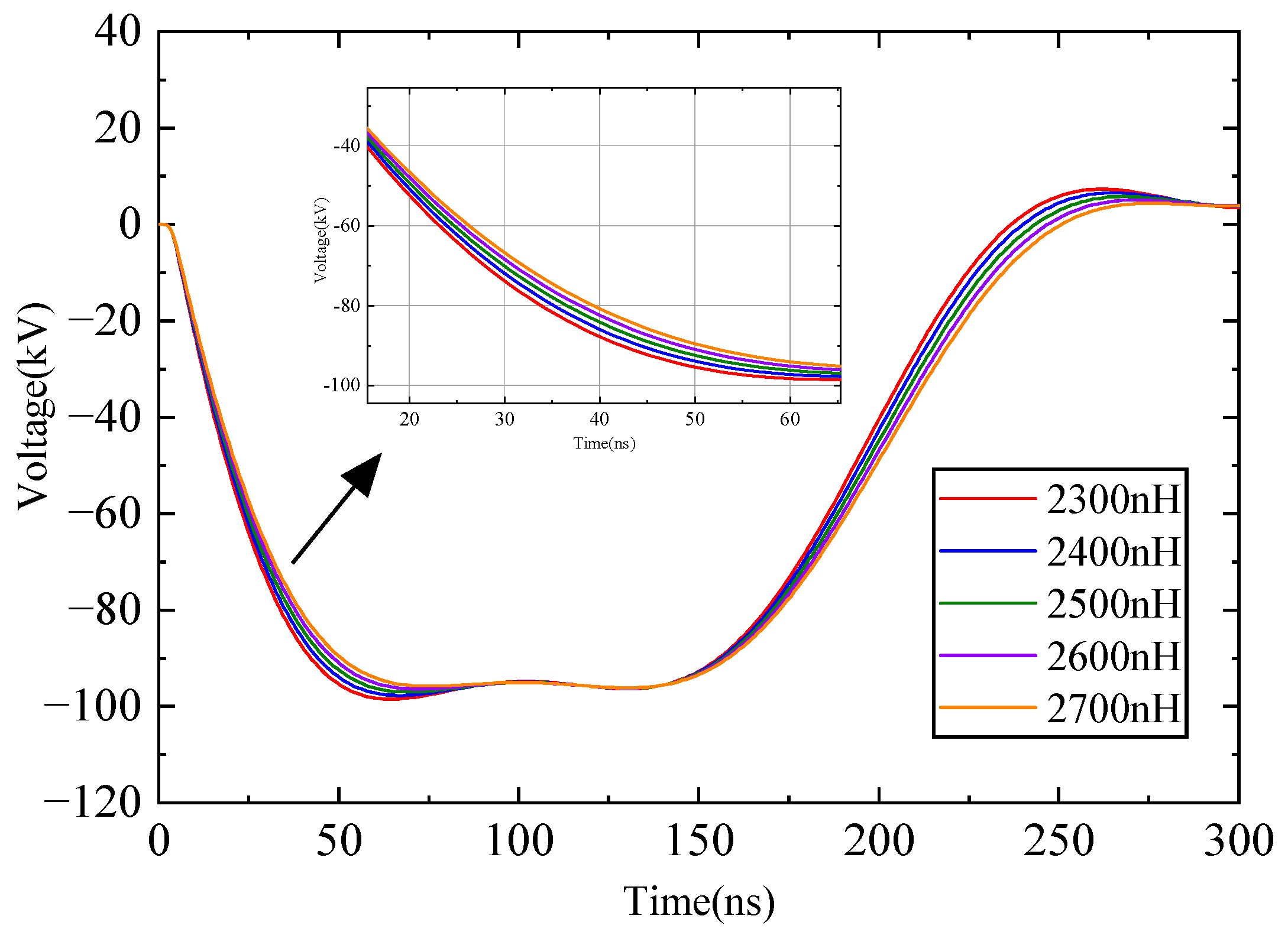
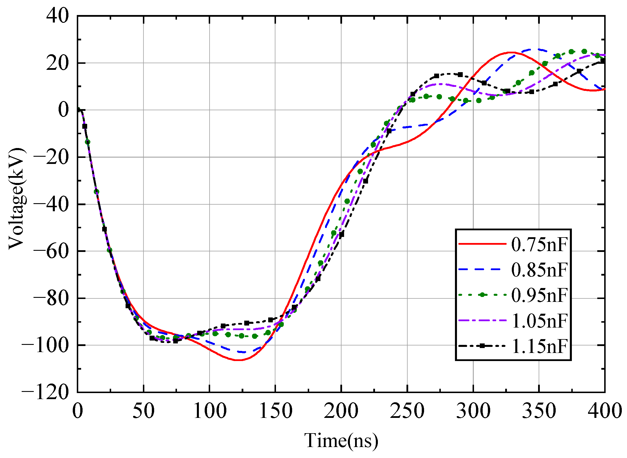
To simplify the analysis, the parameters of the two-section anti-resonant network were varied to observe their effects on the output waveform. Figure 7, Figure 8 and Figure 9 show the influence of the series resonant inductance, parallel resonant inductance, and parallel resonant capacitor on the output voltage, respectively. The series resonant inductance is primarily determined by the loop inductance of the Marx generator itself. Once the Marx generator is designed, the loop inductance changes minimally. As shown in Figure 7, the series resonant inductance has little effect on the output characteristics of the anti-resonant network.
The parallel resonant circuit plays a crucial role in modulating the waveform. Both the parallel resonant inductor and the parallel resonant capacitor influence the slope of the flat-top. However, the parallel resonant capacitor has a greater impact on the waveform. Therefore, the value of the parallel resonant capacitor must meet stricter specifications. Based on the above results, in practice, the modulated capacitor value should be maintained within a 5% relative error of the theoretical value, the parallel modulated inductor value can be maintained within a 10% relative error of the theoretical value, and the series modulated inductor value can be maintained within a 15% relative error of the theoretical value.
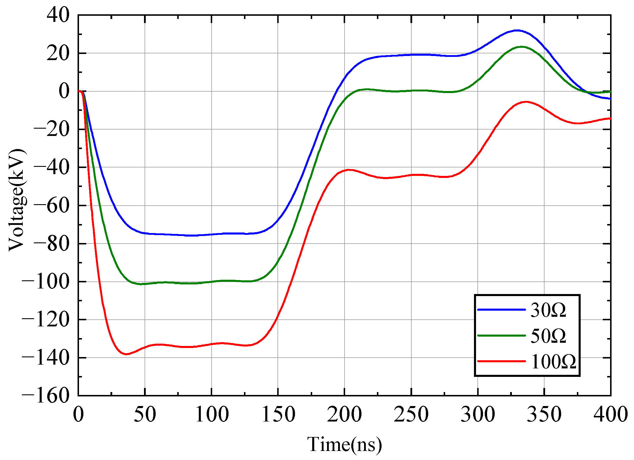
The physical characteristics of high-power microwave loads are typically complex, and their resistance value are not a fixed. To verify the practicality and scalability of the anti-resonant network, the output characteristics of the anti-resonant network under different load impedances are explored. Figure 10 shows the output voltage waveform of the three-section anti-resonant network under different load impedances. Variations in load impedance cause corresponding changes in voltage, and when the impedance is not matched, reflected waves occur in the circuit. However, the waveform at the peak remains stable.
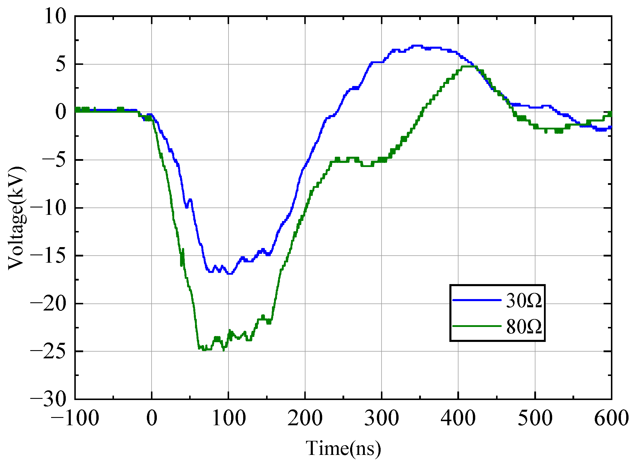
The waveform modulation capability of the anti-resonant network under impedance mismatch conditions was further verified through low-voltage experiments. Taking a three-section anti-resonant network as an example, the output voltage waveforms were measured with loads of 30 Ω and 80 Ω, as shown in Figure 11. Since the low-voltage experiments were conducted in an air environment, slight oscillations appeared on the flat-top of the output waveforms. The experimental results show that when the load was 30 Ω, a reverse pulse occurred. When the load was 80 Ω, a stepped reflected pulse appeared. However, overall, the anti-resonant network was able to ensure the stability of the pulse flat-top, which is consistent with the previous simulation results.

2.6. Anti-Resonant Networks with Stray Parameters

For anti-resonant networks, the most influential stray parameters are the parasitic inductance of the modulation capacitor and the grounding capacitance. In addition, the non-ideal characteristics of the load also affect the output waveform of anti-resonant networks. To clearly identify the influence of stray parameters on the output waveform, different types of stray parameters can be analyzed separately in PSpice.
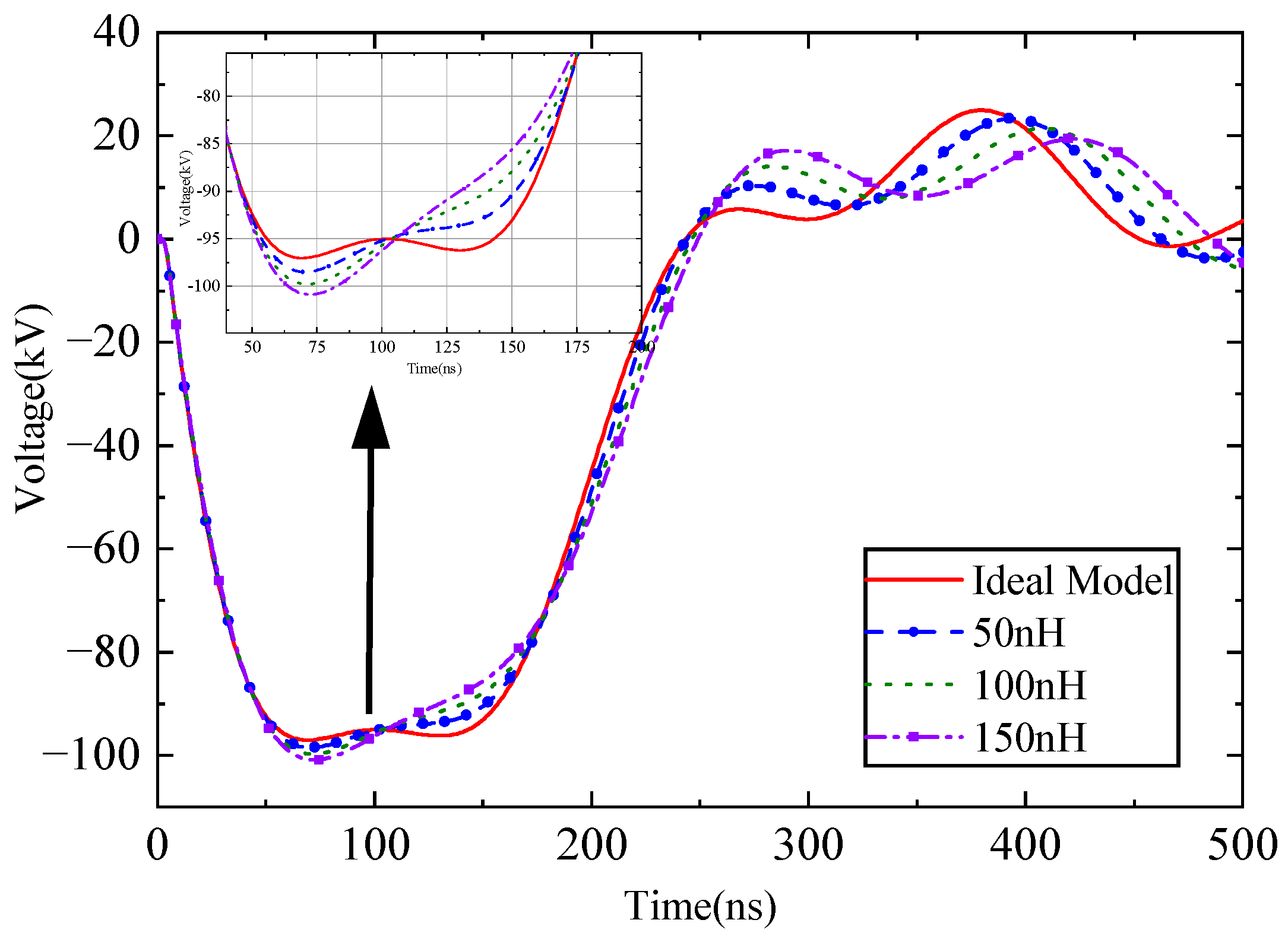
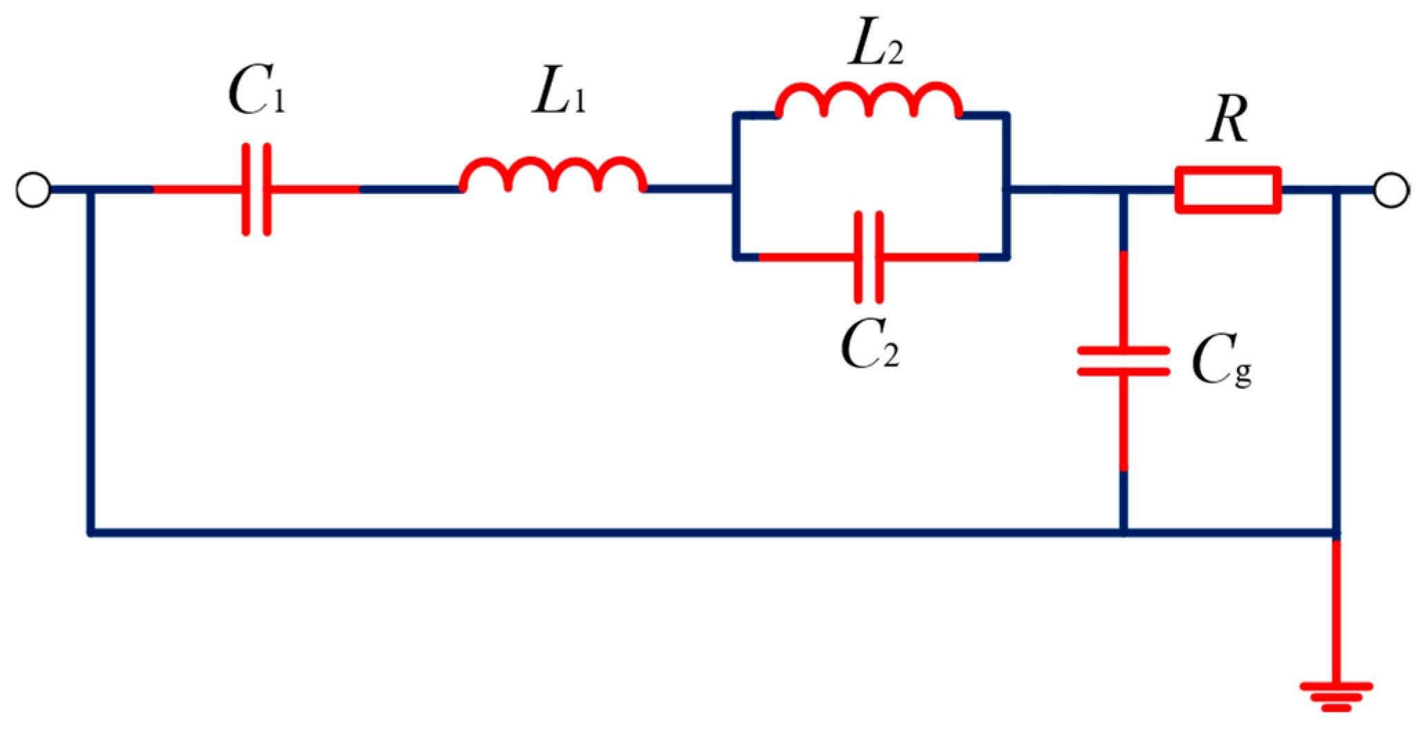
The parasitic inductance of the modulated capacitor primarily arises from its physical structure, such as the ring current loop within the thin-film capacitor. The larger the loop area, the greater the parasitic inductance, typically ranging from tens to hundreds of nanohenries (nH). To simplify the analysis, PSpice is used to calculate the effect of the parasitic inductance of the modulated capacitor on the output voltage waveform in two-section anti-resonant networks. The circuit diagram of a two-section anti-resonant network with parasitic inductance is shown in Figure 12.
The simulation of parameter variations was conducted in PSpice, with parasitic inductance values set at 50 nH, 100 nH, and 150 nH. The results are shown in Figure 13. As illustrated, the parasitic inductance in the modulation capacitor primarily affects the flat-top of the output waveform, causing distortion. As the parasitic inductance value increases, the slope of the pulse flat-top becomes progressively steeper. However, the parasitic inductance has little effect on the leading edge and trailing edge of the waveform.
Since the pulse power source for high-power microwave applications is typically housed within a closed cylinder, the purpose is to reduce external interference and maintain airtightness, which is conducive to the improvement of insulation performance. But being in a cylinder significantly increases the effect of ground capacitance. A circuit diagram of a two-section anti-resonant network with ground capacitance is presented in Figure 14.
The simulation of parameter changes was performed in PSpice, with the ground capacitance values set to 30 pF, 50 pF, and 100 pF. The results are shown in Figure 15. It can be observed that the effect of ground capacitance on the waveform is very minimal, causing only a slight increase in leading edge of the output waveform, while having a negligible for the flat-top of the waveform.
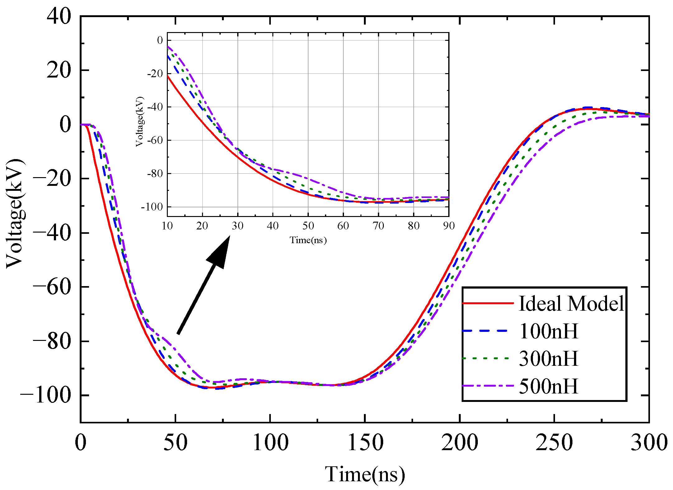
The non-ideal characteristics of the load are typically caused by the parasitic inductance of the resistance. On one hand, the parasitic inductance slows the pulse leading edge by increasing the series inductance of the loop, and on the other hand, it causes waveform distortion by forming a resonant circuit with the ground capacitance. PSpice is used to analyze the influence of different load parasitic inductors on the waveform under the condition of the ground capacitance of 30 pF, as shown in Figure 16. As can be seen from the figure, the leading edge and trailing edge of the waveform are elongated due to the load’s parasitic inductance, resulting in the waveform distortion.

3. Results

3.1. Trigger Source

The first stage switch of the modulated Marx generator designed in this paper uses a trigger switch, while the other switches employ a self-breakdown switch. The first stage utilizes a trigger switch to precisely control the discharge initiation time. The Marx generator based on magnetic switch is used as the trigger source for the first stage, and its circuit schematic is shown in Figure 17:
The secondary inductance in the Marx generator based on the magnetic switch is both used as a charging device and a switching device. When the energy storage capacitor is charged, the secondary inductance is magnetically saturated, the impedance drops rapidly, and it is approximately short-circuited, which in turn causes the series superposition voltage of the energy storage capacitor. The physical photo of the trigger source in the experiment is shown in Figure 18. The number of stages of the Marx generator in the trigger source is 5, and the volume of the trigger source is 400 mm * 230 mm * 150 mm. Transformer oil is used to strengthen the insulation. Since the conduction of all magnetic switches is essentially the saturation of the magnetic core, and all magnetic switches are wound around the same magnetic core, the synchronization of the magnetic switch is perfect. Figure 19 shows the output waveform of the trigger source operating at 20 Hz. The results demonstrate that the output voltage of the trigger source can reach 50 kV, with minimal output voltage jitter.

3.2. Single Experiment

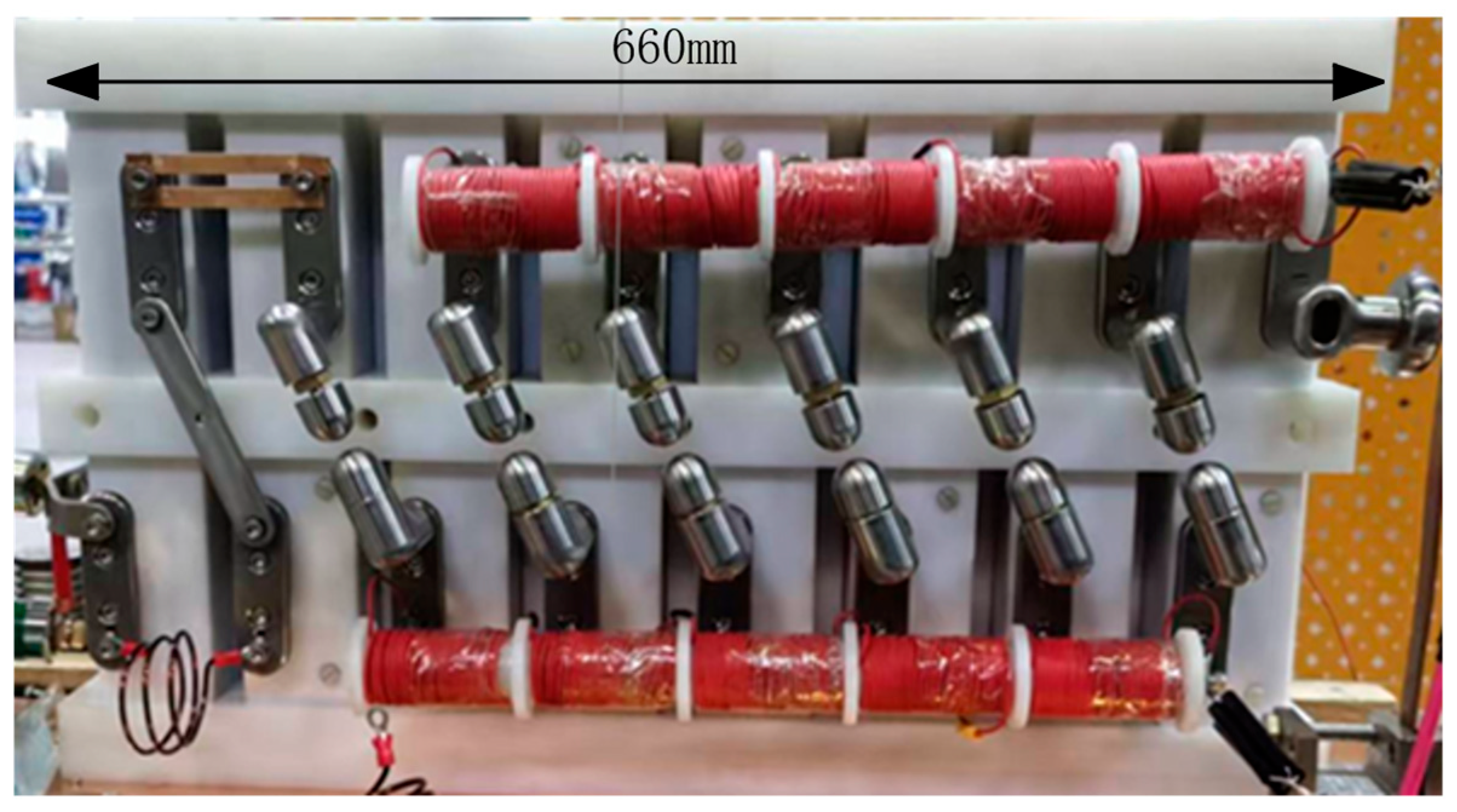
Figure 20 shows the photo of the modulated Marx generator, with all capacitors placed in an insulated frame. The dimensions of the insulated frame are 660 mm in length, 360 mm in width, and 125 mm in height. The charging port of the Marx generator is connected to the output of the pulse air-core transformer. In the experiment, a capacitive voltage divider is used to measure the voltage at the load, and a Rogowski coil is used to measure the current at the load. The sensitivity of voltage divider and Rogowski coil are 3379.3 kV/V and 214.7 A/V, respectively. Since the Rokowski coil is hand-made, it causes slight distortion in the current measurement.
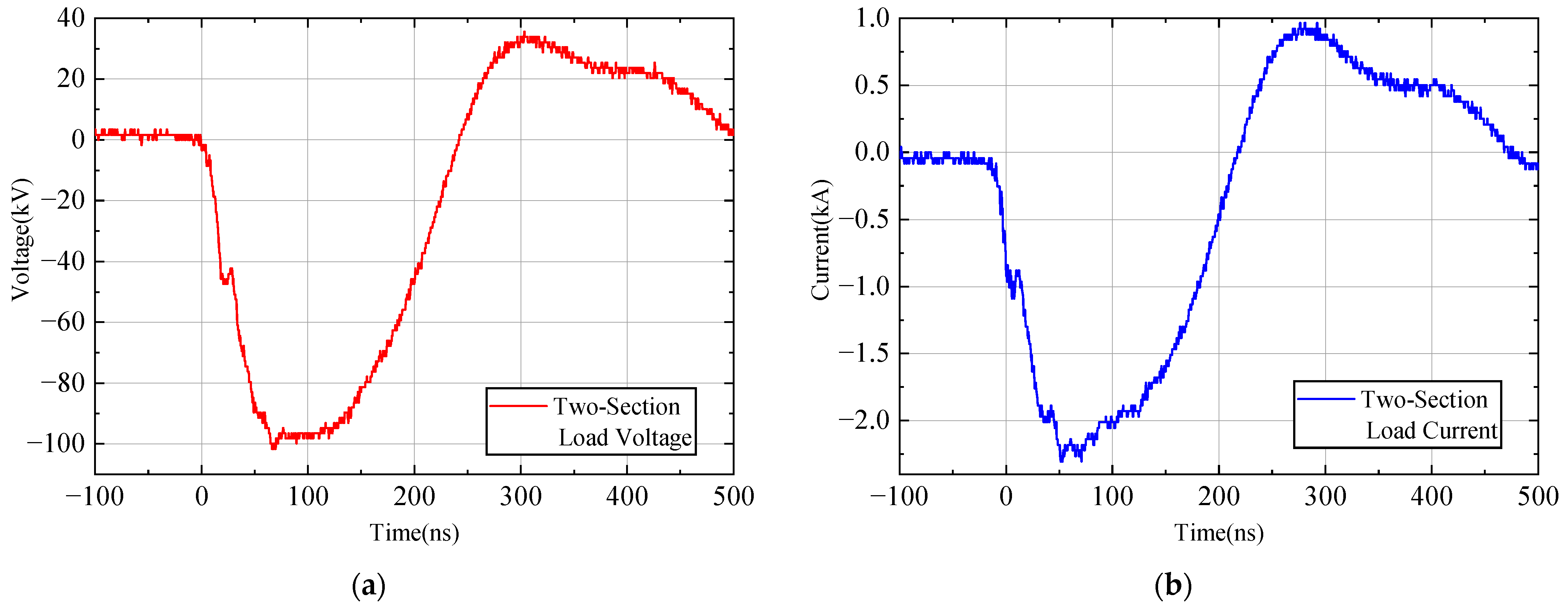
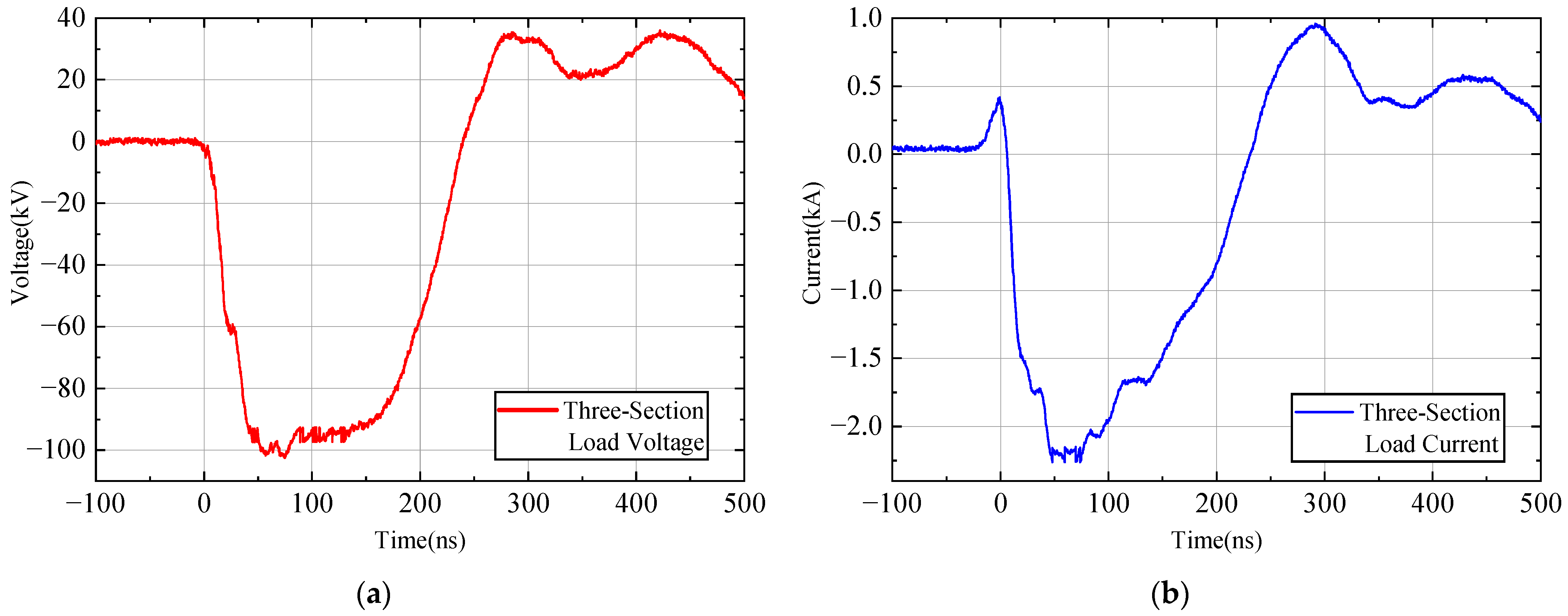
When the primary capacitance was charged to 580 V, the output voltage was measured using a capacitive divider. Figure 21 shows the output waveform of the modulated Marx generator using a two-section anti-resonant network, with a voltage amplitude of approximately 100 kV, a pulse width of about 165 ns, and a rise time of approximately 41 ns. Figure 22 shows the output waveform of the modulated Marx generator using a three-section anti-resonant network, with a voltage amplitude of approximately 100 kV, a pulse width of about 185 ns, and a rise time of approximately 25 ns. The above experimental results (rise time and pulse width) can be consistently reproduced within a 5% margin of error.
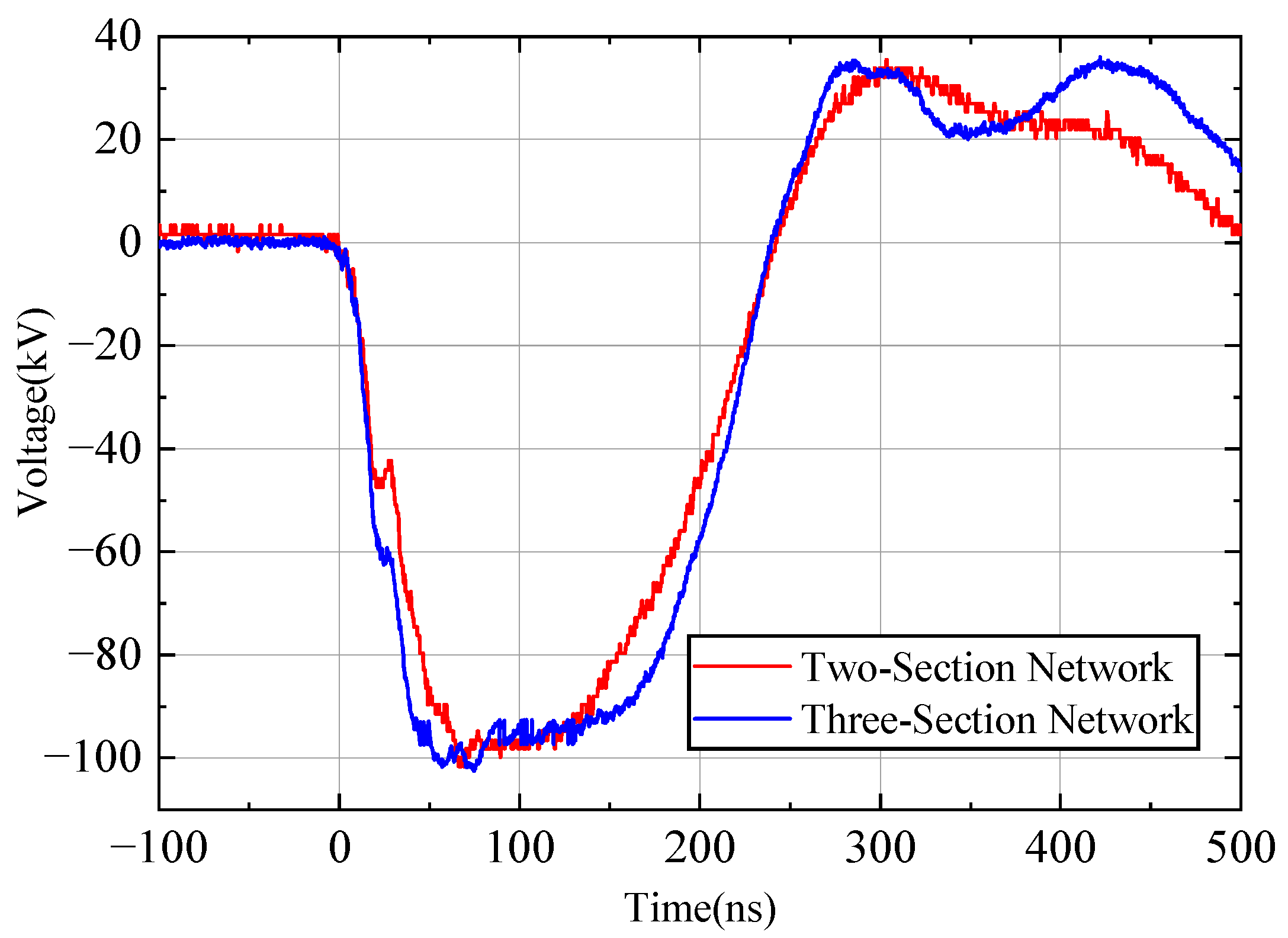
Figure 23 shows a comparison of the output waveforms from the two-section anti-resonant network and the three-section anti-resonant network. The results indicate that the three-section modulation network has a faster rise time and a longer pulse flat-top, which is consistent with the simulation results. Unlike the simulation, the pulse width of the three-section modulation network is longer compared to that of the two-section modulation network.

3.3. Comparison of Simulation and Experiment

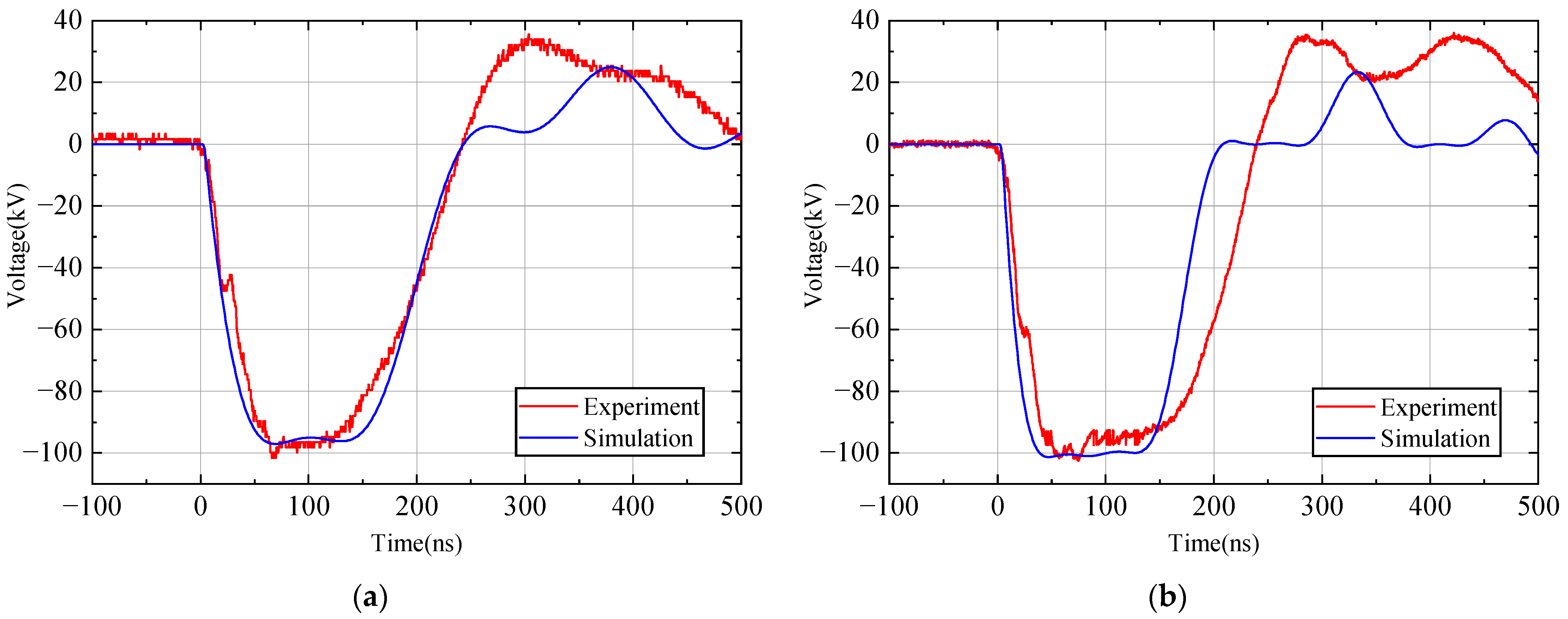
Figure 24 presents a comparison between the experimental and simulation results for the two-section and three-section networks. The experimental results are consistent with the PSpice simulation in terms of waveform trends. However, due to the presence of stray parameters, some waveform distortions occur, resulting in longer rise times and increased pulse widths. The stray parameters in the system include the inductance when the switch is on, the parasitic inductance of the capacitors, and other factors. Additionally, since the device operates in a metal cylinder, the effect of ground capacitance also influences the system.
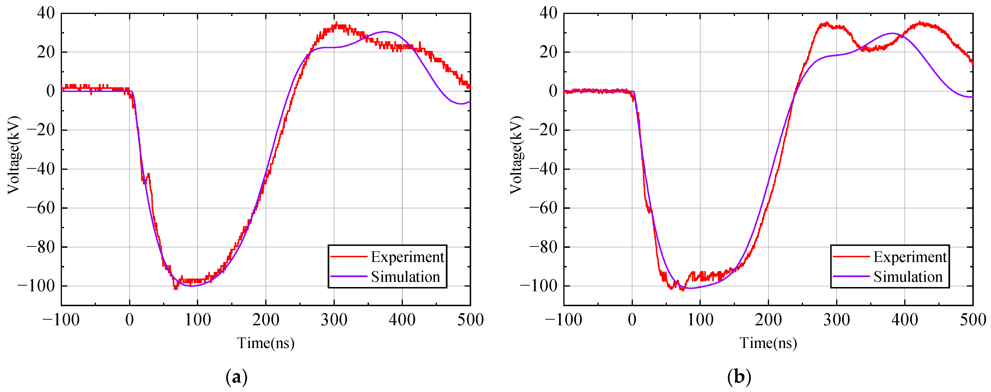
Based on previous analysis of anti-resonant networks, by adding capacitor parasitic inductance and stray grounding capacitance in the simulation and comparing the results with the experimental output waveform shown in Figure 25, it was found that the simulated waveform closely matches the experimental waveform. This comparison validates the previous assumptions.
As shown in Figure 25, stray parameters primarily affect the leading edge, pulse width, and trailing edge of the waveform. The simulation results indicate that the ground capacitance mainly causes an extension of the waveform’s leading and trailing edges, while the parasitic inductance of the capacitor and the switching inductance are the main components of the loop inductance. The loop inductance is equivalent to the first section series inductance in the anti-resonant network. Previous calculations reveal that the loop inductance value in two-section anti-resonant networks is greater than that in three-section anti-resonant networks. This indicates that the increase in the first section series inductance caused by stray inductance has a greater impact on a three-section anti-resonant network, resulting in a longer pulse width compared to a two-section network. Additionally, the parasitic inductance of the capacitor can also affect the parallel modulation network, thereby influencing the modulation performance of the anti-resonant network. This portion of parasitic inductance can lead to the elongation of the waveform’s trailing edge. Since the three-section anti-resonant network contains more parallel resonant networks, the distortion of its waveform is also more severe, which is one of the reasons for the increased pulse width in the three-section anti-resonant network.
Overall, combining simulation and experiment, it can be found that the anti-resonant network has an excellent optimizing effect on the waveform and has great development potential.

3.4. The Energy Efficiency of the System

Energy efficiency is an important metric of the Marx generator, being used to evaluate the performance of a Marx generator circuit design. A Marx generator with high energy efficiency demonstrates greater reliability. According to the energy storage of the energy storage capacitor and the energy obtained by the load, the energy efficiency of the modulated Marx generator can be obtained from Equation (6). In the formula, N is the number of stages of the Marx generator, Cm is the equivalent capacitance of the Marx generator (in farads), Uc is the charging voltage of the energy storage capacitor (in volts), T1 is the pulse start time, and T2 is the pulse end time.
η = 2 T 1 T 2 u ( t ) i ( t ) d t N 2 C m U c 2
According to Equation (6), the energy efficiency of the modulated Marx generator designed in this paper is 75.7%, confirming the high efficiency of the modulated Marx generator based on the anti-resonant network.

3.5. Repetition Experiment

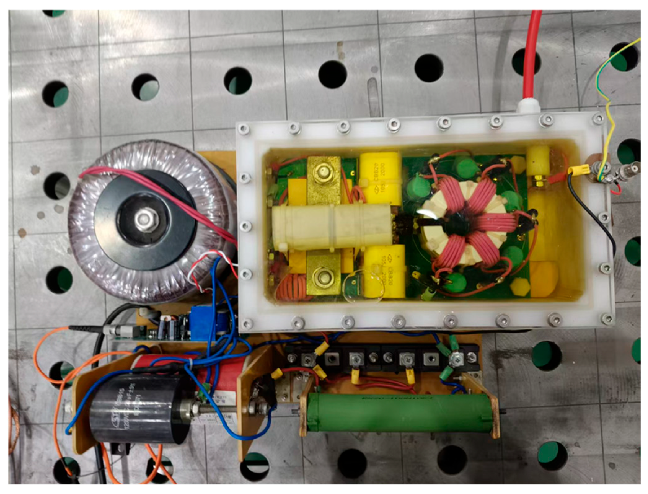
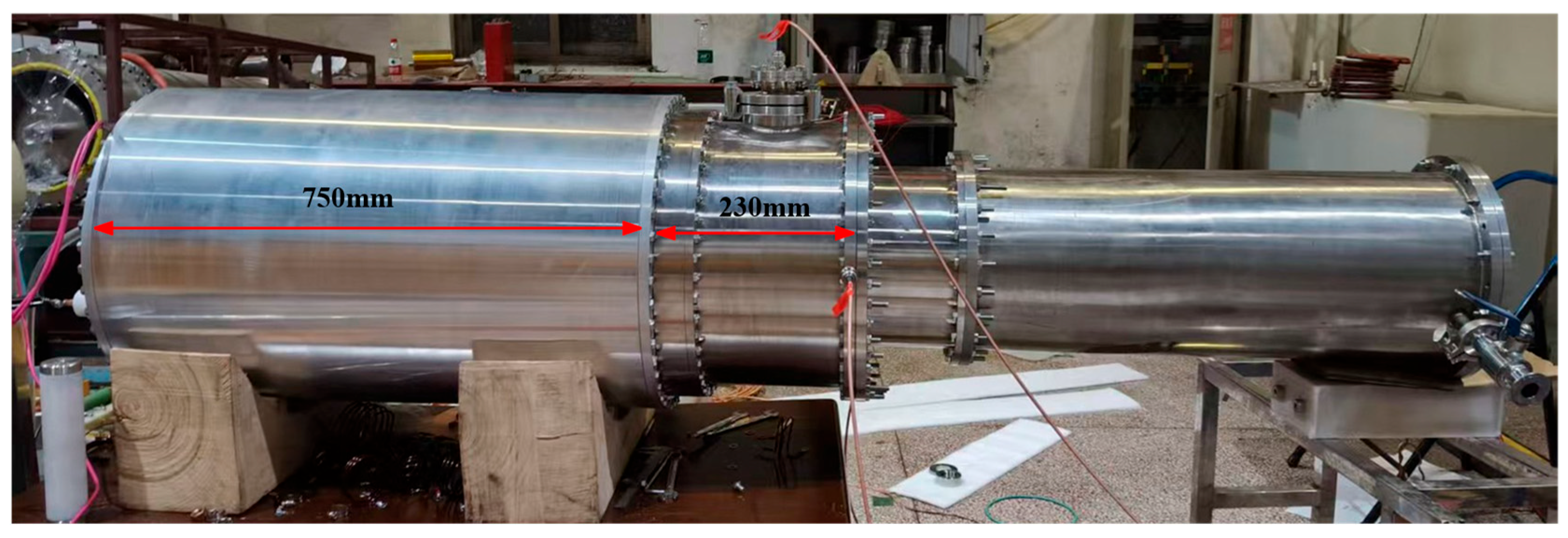
Based on the single experiment system, by adding the charging power supply and the charging control system, the experimental system can operate in burst mode. A mixture of SF6 and N2 gases is filled into the Marx generator to enhance the insulation strength of the system. A complete, real photo of the pulse power source is shown in Figure 26.
The repetition experiment employed a three-section anti-resonant network as the modulation network for the Marx generator. After completing the debugging of the entire pulse power source, the system ran at a repetition frequency of 20 Hz. A quasi-square-wave pulse with an output voltage of 100 kV was obtained on the resistor with a load of 50 Ω, the experimental waveform results are shown in Figure 27. The results show that the output waveform is basically consistent with the single experiment, and the waveform between different pulses is consistent.
In order to evaluate the stability of the designed modulated Marx generator in repetition mode, a total of 100 pulses were output at 20 Hz. The superimposed output voltage waveform is shown in Figure 28. Based on these data, the synchronous jitter σ s was calculated by Equations (7) and (8).
t s ¯ = 1 M i = 1 M t s i
σ s = 1 M i = 1 M ( t s i t s ¯ ) 2
In Formula (7) t s i is the pulse width of the i-th pulse, t s ¯ is the average of the pulse width of all pulses, and M is the number of pulses output. From this, it can be calculated that t s ¯ is 186.214 ns and the synchronous jitter is 1.7614 ns. To further verify the stability of the repeated frequency operation, the average and standard deviation of the pulse rise time were calculated to be 28.764 ns and 0.7465 ns, respectively, while the average and standard deviation of the pulse flatness were 62.89% and 4.45%, respectively. These results indicate that the pulse power source developed in this study exhibits good stability when working in burst mode.

4. Discussion

Currently, the mainstream method for generating square-wave high-voltage pulses involves using Marx generators with equal inductance and capacitance, known as PFN–Marx generators. These typically require multiple network sections to produce a smooth flat-top, and the output waveform often exhibits overshoot, which cannot be mitigated simply by increasing the number of network sections. In order to verify the advantages of waveform modulation using anti-resonant networks, this paper compares its results with those of PFN–Marx generators employed in recent high-power microwave generation. The three selected PFN–Marx generators were designed by Haoran Zhang et al. (2021) [44], Ankur Patel et al. (2022) [45], and Liyang Huang et al. (2023) [6]. The comparison of design parameters is shown in Table 2.
The PFN–Marx generator designed by Haoran Zhang employs a modulation network consisting of three equal-value PFN sections. However, the relatively small number of modulation sections results in the poorest waveform flatness. Despite this, the limited number of network sections and the compact design yield a very high J/L ratio for the generator. In contrast, the PFN–Marx generator designed by Ankur Patel uses a modulation network with eight equal-value PFN sections, producing a relatively flat output voltage waveform overall. Nevertheless, due to the characteristics of equal capacitance and inductance pulse-forming networks, the leading edge of its output voltage waveform exhibits a noticeable overshoot. The PFN–Marx generator designed by Liyang Huang incorporates a modulation network with twelve equal-value PFN sections and adjusts the output waveform by adding inductors at both ends of the switch. This approach mitigates the overshoot issue in the output voltage waveform. However, the addition of inductors may cause impedance mismatches, which in turn reduce waveform flatness. Comparing these PFN–Marx generators reveals that a three-section anti-resonant network achieves the best waveform flatness and the smallest rising edge ratio, while also using the fewest modulation network sections. This comparison demonstrates that a modulated Marx generator based on an anti-resonant network can produce a superior output voltage waveform with fewer modulation network sections.
Overall, both simulation and experimental results show that the anti-resonant network has great advantages in pulse waveform modulation. The anti-resonant network has the ability to generate square-wave pulses with durations of 100 to 200 ns and requires fewer sections than traditional PFN. In practical applications of high-power microwaves, the anti-resonant network is directly cascaded after the Marx generator for modulation. Compared to the PFN–Marx integrated modulation and voltage boosting, the pulse power source based on the anti-resonant network can achieve flexible waveform modulation by directly changing the component values within the anti-resonant network or by replacing the network structure. In short pulse modulation, pulse-forming lines are also commonly used for modulation. Compared to pulse-forming lines, the anti-resonant network is more compact in size and has better environmental adaptability. Due to the specificity of the parameters of the anti-resonant network, precise control of component parameters is required in practice, especially the modulation capacitor. Although it has lower sensitivity to parasitic parameters compared to the equivalent PFN, as the number of sections in the network increases, the anti-resonant network also becomes more susceptible to the effects of parasitic parameters. Limited by switch jitter and the insulation recovery time of the mixed gas, the pulse power source developed in this paper can currently operate stably at 20 Hz. With the continuous advancement of high-power microwave technology, pulse power technology is moving toward higher voltages and higher repetition frequency. Against this background, our upcoming research will focus on developing a modulated Marx generator capable of operating at higher voltage levels and higher repetition frequency.

Author Contributions

Conceptualization, R.L. and X.C.; methodology, Z.P.; validation, R.L. and X.Z.; formal analysis, R.L.; investigation, R.L.; resources, R.C.; writing—original draft preparation, R.L.; writing—review and editing, X.C. and R.C.; supervision, X.C.; project administration, X.C.; funding acquisition, X.C. All authors have read and agreed to the published version of the manuscript.

Funding

This research received no external funding.

Data Availability Statement

The data that support the findings of this study are available from the corresponding author upon reasonable request.

Acknowledgments

The authors would like to thank Xia Chen and Min Zhu for their support and assistance during assembly and experimentation.

Conflicts of Interest

The authors declare no conflicts of interest.

References

  1. Zhang, J.; Ge, X.; Zhang, J.; Zhang, J.; He, J.; Fan, Y.; Li, Z.; Jin, Z.; Gao, L.; Ling, J.; et al. Research progresses on Cherenkov and transit-time high-power microwave sources at NUDT. Matter Radiat. Extrem. 2016, 1, 163–178. [Google Scholar] [CrossRef]
  2. Rubery, M.; Kemp, G.; Jones, M.; Pelepchan, N.; Stolte, W.; Heinmiller, J. Soft x-ray power diagnostics for fusion experiments at NIF, Omega, and Z facilities. Rev. Sci. Instrum. 2023, 94, 031101. [Google Scholar] [CrossRef]
  3. Akiyama, H.; Sakai, S.; Sakugawa, T.; Namihira, T. Environmental applications of repetitive pulsed power. IEEE Trans. Dielectr. Electr. Insul. 2007, 14, 825–833. [Google Scholar] [CrossRef]
  4. Zhang, Z.; Zhou, Y.; Zhang, Y.; Yang, F.; Ge, X.; He, J. Waveform response to high power microwave pulse in time-division multiplexing RF front end. High Power Laser Part Beams 2023, 35, 103004-1–103004-7. [Google Scholar]
  5. Ding, Y.; Abe, D.; Shen, B.; Gao, D.; Ding, H. An Overview of Multibeam Klystron Technology. IEEE Trans. Electron Devices 2023, 70, 2656–2665. [Google Scholar] [CrossRef]
  6. Huang, L.; Xiang, Z.; Deng, B.; Wang, H.; Yuan, Y.; Mao, Q.; Cui, Y.; Xie, M.; Meng, J. Compact Gigawatt Pulsed Power Generator for High-Power Microwave. IEEE Trans. Electron Devices 2023, 70, 3885–3891. [Google Scholar] [CrossRef]
  7. Xun, T.; Zhao, Y.; Yang, H.; Hu, T.; Zhang, Z.; Cheng, X.; Zhang, J.; Zhang, J.; Zhong, H. Developments of Pulsed Electron Beam Sources for High-Power Microwave Applications. IEEE Access 2020, 8, 101351–101358. [Google Scholar] [CrossRef]
  8. Andreev, A.; Bosman, H.; Schamiloglu, E. Simulation of Anode Material Erosion in the Internal Environment of HPM Devices. In Proceedings of the IEEE International Conference on Plasma Science, Monterey CA, USA, 20–23 June 2005. [Google Scholar]
  9. Schamiloglu, E. High power microwave sources and applications. In Proceedings of the IEEE MTT-S International Microwave Symposium Digest, Fort Worth, TX, USA, 6–11 June 2004. [Google Scholar]
  10. Ghosh, P.; Chaudhury, B. Investigation of Microwave Induced Local Gas Heating in HPM Switching and Protection Using Two-dimensional Computations. In Proceedings of the IEEE Microwaves, Antennas, and Propagation Conference, Bangalore, India, 12–16 December 2022. [Google Scholar]
  11. Zhang, J.; Jin, Z.; Yang, J.; Zhang, D.; Shu, T.; Zhang, J.; Zhong, H. Successful Suppression of Pulse Shortening in an X-Band Overmoded Relativistic Backward-Wave Oscillator with Pure TM01 Mode Output. IEEE Trans. Plasma Sci. 2015, 43, 528–531. [Google Scholar] [CrossRef]
  12. Gao, J.; Li, S.; Qian, B.; Zhang, J.; Zhang, J.; Yang, H. Development of a GW-Level Solid-State Long Pulse Generator. IEEE Trans. Plasma Sci. 2019, 47, 4512–4517. [Google Scholar] [CrossRef]
  13. Wang, L.; Zhang, Z.; Liu, Q.; Zhang, T. Development of a 500-kV All Solid-State Linear Transformer Driver. IEEE Trans. Plasma Sci. 2021, 49, 1915–1919. [Google Scholar] [CrossRef]
  14. Niu, X.; Wu, Q.; Wang, B.; Yao, J.; Chu, X.; Yi, M.; Gu, Y.; Wang, L.; Xun, T.; Yang, H. Test of KW Class Photonic Microwave Generation Using Vanadium-Compensated 6H-SiC PCSS and Burst-Mode-Operation Pulse Laser. IEEE Photonics J. 2023, 15, 1–7. [Google Scholar] [CrossRef]
  15. Liu, Z.; Huang, H.; Jin, X.; Li, S.; Wang, T.; Fang, X. Investigation of an X-Band Long Pulse High-Power High-Gain Coaxial Multibeam Relativistic Klystron Amplifier. IEEE Trans. Electron Devices 2019, 66, 722–728. [Google Scholar] [CrossRef]
  16. Appiah, G.; Martinez, D.; Albarracin, F.; Kasmi, C.; Mora, N. Analytical Design and Simulation of a 9.3GW Tesla Transformer for HPM Sources. IEEE Trans. Plasma Sci. 2022, 50, 4897–4904. [Google Scholar] [CrossRef]
  17. Shanmuganathan, U.; Saket, K.; Kumar, S.; Das, K.; Nekkanti, S.; Gupta, K. A Compact Repetitive Marx Generator for Generating Intense Electron Beams for HPM Sources. IEEE Trans. Electron Devices 2023, 70, 1256–1261. [Google Scholar] [CrossRef]
  18. Belozerov, O.; Krasik, Y.; Leopold, J.; Pavlov, S.; Hadas, Y.; Kuchuk, K.; Schamiloglu, E. Characterizing the high-power-microwaves radiated by an axial output compact S-band A6 segmented magnetron fed by a split cathode and powered by a linear induction accelerator. J. Appl. Phys. 2023, 133, 133301. [Google Scholar] [CrossRef]
  19. Sporer, B.; Shah, A.; Dowhan, G.; Shapovalov, R.; Packard, D.; Wisher, M.; Leckbee, J.; Hendricks, K.; Hoff, B.; Lau, Y.; et al. Multicavity linear transformer driver facility for Z-pinch and high-power microwave research. Phys. Rev. Accel. Beams 2021, 24, 100402. [Google Scholar] [CrossRef]
  20. Benford, J. History and Future of High Power Microwaves. IEEE Trans. Plasma Sci. 2024, 52, 1137–1144. [Google Scholar] [CrossRef]
  21. Jordan, N.; Greening, G.; Exelby, S.; Packard, D.; Lau, Y.; Gilgenbach, R. Pulse Shortening in Recirculating Planar Magnetrons. IEEE Trans. Electron Devices 2018, 65, 2354–2360. [Google Scholar] [CrossRef]
  22. Benford, J.; Benford, G. Survey of pulse shortening in high-power microwave sources. IEEE Trans. Plasma Sci. 1997, 25, 311–317. [Google Scholar] [CrossRef]
  23. Zhang, Y.; Shao, H.; Sun, J.; Song, Z.; Zhang, X. Investigation of Pulse Shortening Suppressions on the Coaxial Vircator. In Proceedings of the Progress in Electromagnetic Research Symposium, Shanghai, China, 8–11 August 2016. [Google Scholar]
  24. Chung, S. Particle-In-Cell Simulations on Long Pulse Large Current Behavior of Magnetron with Diffraction Output. IEEE Trans. Plasma Sci. 2022, 50, 2085–2096. [Google Scholar] [CrossRef]
  25. Yuan, Y.; Meng, J.; Zhang, J.; Zhu, D.; Cui, Y. Influence of RF Breakdown Plasma on Dispersion Relation of High Frequency Structures and Characteristics of Generated Microwave in Relativistic Backward Wave Oscillators. In Proceedings of the Photonics & Electromagnetics Research Symposium, Xiamen, China, 17–20 December 2019. [Google Scholar]
  26. Cao, Y.; Sun, J.; Fan, Z.; Wu, P.; Song, Z.; Zhu, M.; Bai, X. Plasma effects in the relativistic backward wave oscillator. In Proceedings of the IEEE International Conference on Plasma Science, Beijing, China, 16–20 June 2024. [Google Scholar]
  27. Ge, X.; He, J.; Ju, J.; Ling, J.; Song, L. Long-pulse high-efficiency relativistic Cherenkov oscillators at L-and S-bands. In Proceedings of the International Conference on Infrared, Millimeter, and Terahertz Waves, Paris, France, 1–6 September 2019. [Google Scholar]
  28. Benford, J.; Benford, G. Pulse shortening in high power microwave sources. In Proceedings of the IEEE International Pulsed Power Conference, Baltimore, MD, USA, 29 June–2 July 1997. [Google Scholar]
  29. Hendricks, K.; Haworth, M.; Spencer, T.; Shiffler, D.; Arman, M.; Hackett, K. Research on pulse shortening of GW class HPM sources. In Proceedings of the IEEE Conference Record-Abstracts. 1996 IEEE International Conference on Plasma Science, Boston, MA, USA, 3–5 June 1996. [Google Scholar]
  30. Zhang, Z.; Zhou, Y.; Zhang, Y.; Qian, B. Investigation on the Effect of HPM Pulse Width and Repetition Frequency on the AAV. IEEE Trans. Electromagn. Compat. 2024, 67, 530–537. [Google Scholar] [CrossRef]
  31. Luo, J.; Feng, J.; Gong, Y. A Review of Microwave Vacuum Devices in China: Theory and Device Development Including High-Power Klystrons, Spaceborne TWTs, and Gyro-TWTs. IEEE Microw. Mag. 2021, 22, 18–33. [Google Scholar] [CrossRef]
  32. Pouncey, J.; Lehr, J.; Giri, D. Erection of Compact Marx Generators. IEEE Trans. Plasma Sci. 2019, 47, 2902–2909. [Google Scholar] [CrossRef]
  33. Song, F.; Li, F.; Zhang, B.; Zhu, M.; Li, C.; Wang, G.; Gong, H.; Gan, Y.; Jin, X. Recent advances in compact repetitive high-power Marx generators. Laser Part Beams 2019, 37, 110–121. [Google Scholar] [CrossRef]
  34. Zhang, H.; Yang, J.; Lin, J.; Yang, X. A compact bipolar pulse-forming network-Marx generator based on pulse transformers. Rev. Sci. Instrum. 2014, 84, 114705. [Google Scholar] [CrossRef]
  35. Aranganadin, K.; Zhang, Z.; Lin, Y.; Chang, P.; Hsu, H.; Lin, M. A Mini-Marx Generator Powered by a Cockcroft-Walton Voltage Multiplier. IEEE Trans. Plasma Sci. 2022, 50, 3393–3399. [Google Scholar] [CrossRef]
  36. Liu, S.; Zhang, J.; Zhang, Z. Review of high power compact pulse forming network-Marx generators. High Power Laser Part Beams 2022, 34, 075001. [Google Scholar]
  37. Zhang, H.; Li, Z.; Zhang, Z.; Shu, T. Investigation on the generation of high voltage quasi-square pulses with a specific two-node PFN-Marx circuit. Rev. Scientific. Instrum. 2020, 91, 024702. [Google Scholar] [CrossRef] [PubMed]
  38. Koseki, K. The fast extraction kicker power supply for the main ring of J-PARC. Nucl. Instrum. Methods Phys. Res. Sect. A Accel. Spectrometers Detect. Assoc. Equip. 2013, 729, 3–7. [Google Scholar] [CrossRef]
  39. Song, F.; Zhang, B.; Li, C.; Li, F.; Wang, G.; Gong, H.; Gan, Y.; Jin, X. Development and testing of a three-section pulse-forming network and its application to Marx circuit. Laser Part Beams 2019, 37, 408–414. [Google Scholar] [CrossRef]
  40. Chen, R.; Yang, J.; Cheng, X.; Pan, Z. An all-solid-state microsecond-range quasi-square pulse generator based on fractional-turn ratio saturable pulse transformer and anti-resonance network. Rev. Scientific. Instrum. 2017, 88, 034701. [Google Scholar] [CrossRef] [PubMed]
  41. Cheng, X.; Hu, Y.; Chen, R.; Yang, J.; Pan, Z. A sub-microsecond-range pulse generator based on antiresonance network and transmission line transformer. Rev. Sci. Instrum. 2019, 90, 094703. [Google Scholar] [CrossRef] [PubMed]
  42. Wu, H.; Ding, M.; Zhao, Y.; Feng, Y.; Wang, X.; Li, X. Compact fast raising-edge X-ray system. High Power Laser Part Beams 2014, 26, 055005. [Google Scholar]
  43. Cheng, X.; Chen, R.; Pan, Z.; Yang, J.; Geng, J. Research on a modularized long pulse generator based on anti-resonance network and transmission line transformer. Rev. Sci. Instrum. 2021, 92, 044702. [Google Scholar] [CrossRef]
  44. Zhang, H.; Shu, T.; Liu, S.; Zhang, Z.; Song, L.; Zhang, H. A compact Modular 5GW Pulse PFN-Marx Generator for Driving HPM Source. Electronics 2021, 10, 545. [Google Scholar] [CrossRef]
  45. Patel, A.; Chandra, R.; Basak, A.; Senthil, K.; Roy, A. Design, simulation, and development of bipolar pulse forming network based Marx generator for S band backward wave oscillator. Rev. Sci. Instrum. 2022, 93, 094703. [Google Scholar] [CrossRef] [PubMed]
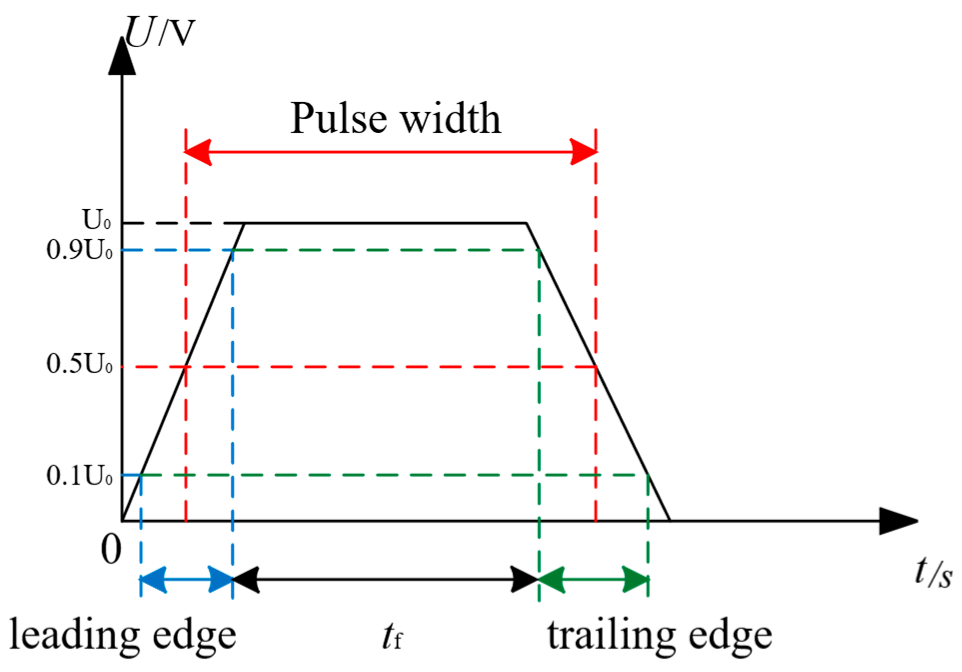
Figure 1. Schematic of the pulse waveform’s metrics.
Electronics 14 03517 g001
Figure 2. System schematic of the modulated Marx circuit.
Electronics 14 03517 g002
Figure 3. Circuit diagram of the Marx generator.
Electronics 14 03517 g003
Figure 4. Structure diagram of the modulated Marx generator.
Electronics 14 03517 g004
Figure 5. Circuit diagram of the N-section anti-resonant network.
Electronics 14 03517 g005
Figure 6. Simulation results of the modulated Marx generator using the two-section anti-resonant network and the three-section anti-resonant network.
Electronics 14 03517 g006
Figure 7. Output voltage waveforms of anti-resonant networks with different series resonant capacitors (red line: 2300 nH, blue line: 2400 nH, green line: 2500 nH, purple line: 2600 nH, orange line: 2700 nH).
Electronics 14 03517 g007
Figure 8. Output voltage waveforms of anti-resonant networks with different parallel resonant inductors (red line: 300 nH, blue dashed line: 365 nH, green dotted line: 430 nH, purple dashed line: 495 nH, black dotted line: 560 nH).
Electronics 14 03517 g008
Figure 9. Output voltage waveforms of anti-resonant networks with different parallel resonant capacitors (red line: 0.75 nF, blue dashed line: 0.85 nF, green dotted line: 0.95 nF, purple dashed line: 1.05 nH, black dotted line: 1.15 nF).
Electronics 14 03517 g009
Figure 10. Output voltage waveforms of the three-section anti-resonant network with different load impedances.
Electronics 14 03517 g010
Figure 11. Experimental results of the output voltage of the three-section anti-resonant network under different load impedances.
Electronics 14 03517 g011
Figure 12. Two-section anti-resonant network circuit with parasitic inductance.
Electronics 14 03517 g012
Figure 13. Influence of parasitic inductance of modulated capacitor on output voltage waveform (signal presents output voltage with different parasitic inductance of modulated capacitor).
Electronics 14 03517 g013
Figure 14. Two-section anti-resonant network circuit with ground capacitance.
Electronics 14 03517 g014
Figure 15. Influence of ground capacitance on output voltage waveform (signal presents output voltage with different ground capacitance).
Electronics 14 03517 g015
Figure 16. Influence of parasitic inductance of resistance on output voltage waveform (signal presents output voltage with different parasitic inductance of resistance).
Electronics 14 03517 g016
Figure 17. Circuit diagram of the trigger source.
Electronics 14 03517 g017
Figure 18. Photo of the trigger source.
Electronics 14 03517 g018
Figure 19. Output voltage diagram of the trigger source at 20 Hz.
Electronics 14 03517 g019
Figure 20. Photo of the modulated Marx generator.
Electronics 14 03517 g020
Figure 21. Experimental results of the modulated Marx generator with a two-section anti-resonant network with 580 V charging voltage and 50 Ω load: (a) load voltage; (b) load current.
Electronics 14 03517 g021
Figure 22. Experimental results of the modulated Marx generator with a three-section anti-resonant network with 580 V charging voltage and 50 Ω load: (a) load voltage; (b) load current.
Electronics 14 03517 g022
Figure 23. Comparison of output voltages of the modulated Marx generator with a two-section anti-resonant network and a three-section anti-resonant network under charging voltage of 580 V and load of 50 Ω.
Electronics 14 03517 g023
Figure 24. Comparison of experimental results and simulation results: (a) Marx generator output voltage with a two-section anti-resonant network; (b) Marx generator output voltage with a three-section anti-resonant network.
Electronics 14 03517 g024
Figure 25. Comparison of experimental results and corrected simulation results: (a) Marx generator output voltage with a two-section anti-resonant network; (b) Marx generator output voltage with a three-section anti-resonant network.
Electronics 14 03517 g025
Figure 26. Photo of the pulse power source.
Electronics 14 03517 g026
Figure 27. Screenshot of the pulse waveform at 20 Hz.
Electronics 14 03517 g027
Figure 28. Waveform superposition of 100 pulses at 20 Hz.
Electronics 14 03517 g028
Table 1. Settings of simulation.
Parameters/SettingsValues/Configurations
solverTransient Analysis
time step1 ns
switch on-time30 ns
switch closed resistance0.01 Ω
final time1000 ns
Table 2. Comparison of design parameters.
ParametersTwo-SectionThree-SectionHaoran Zhang [44]Ankur Patel [45]Liyang Huang [6]
Pulse width (ns)1651859520093
Leading edge (ns)4125286035
Leading edge percentage24.85%13.51%29.47%30%37.63%
Waveform flatness (90%)54.54%63.78%42.11%62.5%53.76%
Waveform flatness (80%)66.06%77.8%73.68%75%64.52%
The number of stages of the Marx generator 1212221824
The number of sections of the modulation network123812
Volume (L)31.3335.8176.923418.051000
Energy density (J/L)1.05330.921536.50.46810.465
Load (Ω)5050598040
Disclaimer/Publisher’s Note: The statements, opinions and data contained in all publications are solely those of the individual author(s) and contributor(s) and not of MDPI and/or the editor(s). MDPI and/or the editor(s) disclaim responsibility for any injury to people or property resulting from any ideas, methods, instructions or products referred to in the content.