Article

Redundancy-Interpolated Three-Segment DAC with On-Chip Digital Calibration for Improved Static Linearity

Department of Electrical and Computer Engineering, Iowa State University, Ames, IA 50011, USA
*
Author to whom correspondence should be addressed.
Electronics 2025, 14(17), 3477; https://doi.org/10.3390/electronics14173477 (registering DOI)
Submission received: 16 July 2025 / Revised: 25 August 2025 / Accepted: 28 August 2025 / Published: 30 August 2025

Abstract

This paper presents a three-segment interpolating Digital-to-Analog Converter (DAC) that employs a redundancy-based interpolation scheme and digital calibration to enhance linearity. The proposed architecture consists of a Most Significant Bit (MSB) resistor string DAC, an Intermediate Significant Bit (ISB) resistor string DAC, and a Least Significant Bit (LSB) interpolating differential buffer. The MSB segment uses a split-unit resistor structure ( r A , r B ) to improve post-calibration differential nonlinearity (DNL) by minimizing voltage step errors. A fully digital calibration algorithm is implemented to compensate for process variations, component mismatches, and finite switch resistance, ensuring a highly linear DAC output. The proposed 16-bit DAC is implemented in a 180 nm CMOS process and is segmented into a 5-bit MSB stage, a 5-bit ISB stage, and a 6-bit LSB stage. The structure achieves post-calibration integral nonlinearity (INL) and differential nonlinearity (DNL) values of less than ±1 LSB. Simulation results validate the proposed design, demonstrating enhanced linearity and reduced area overhead compared with conventional segmented architectures.

1. Introduction

With the advent of the Internet of Things (IoT), the semiconductor industry has witnessed an unprecedented demand for low-power, small-area, and high-functioning integrated circuits [1,2]. This trend has been historically propelled by the relentless pace of Moore’s Law, which has enabled the exponential scaling of digital logic, leading to more powerful processors, larger memories, and more complex digital systems on a single chip [3]. This miniaturization has been a key enabler of the proliferation of smart devices, from wearable health monitors and remote environmental sensors to complex industrial automation systems [4,5]. These applications universally demand long battery life and compact form factors, placing stringent constraints on the power consumption and physical footprint of their electronic components [6].
While digital circuits have thrived under Moore’s Law, the same cannot be said for their analog counterparts. Analog and mixed-signal circuits, which form the critical interface between the digital processing core and the physical world, face a scaling crisis. As transistor dimensions shrink into deep sub-micron regimes, analog performance metrics often degrade. Lower supply voltages reduce the available signal headroom and dynamic range, while the decreased intrinsic gain of short-channel transistors makes designing high-performance amplifiers more difficult. Furthermore, the inherent variability and mismatch of components increase at smaller scales. This dichotomy presents a formidable challenge for designers of Systems on a Chip (SoCs), where the performance of the entire system is often bottlenecked by its analog front-end [7,8]. Among the most critical of these analog blocks is the Digital-to-Analog Converter (DAC), which is fundamental for applications requiring signal synthesis, actuation, or control.
Among the available DAC architectures, the resistor string DAC, often referred to as the R-string or string DAC, remains a popular choice, particularly for applications where low power consumption and inherent monotonicity are crucial [9]. The architecture’s elegance lies in its simplicity: a series of identical resistors form a voltage divider, and a set of switches select a specific tap point to generate the desired analog output voltage. Because selecting a physically higher tap on the string can only ever produce a higher or equal voltage, the architecture is inherently monotonic by design [9,10]. This property is highly desirable since it guarantees that the output will consistently increase or remain constant for increasing digital input codes, preventing the large-scale errors associated with non-monotonic behavior [10].
The principal drawback of the non-segmented string DAC is its prohibitive area cost at higher resolutions [10,11]. A standard n-bit implementation requires an array of 2 n unit resistors and 2 n switches, together with an n-to- 2 n thermometer decoder. As the resolution n increases, this exponential growth in component count leads to an impractically large silicon footprint [12]. To circumvent this scaling issue, designers almost universally employ segmentation. In a segmented design [12,13], the DAC is partitioned into two or more sub-DACs. In a typical two-stage arrangement, an n 1 -bit coarse DAC selects a voltage range and an n 2 -bit fine DAC interpolates within that range. This approach reduces the component count to approximately 2 n 1 + 2 n 2 , making high-resolution designs practical [11,14]. The concept can be extended to a three-segment architecture comprising Most Significant Bit (MSB), Intermediate Significant Bit (ISB), and Least Significant Bit (LSB) stages.
Although segmentation removes the raw area problem [15,16,17], it introduces new challenges that compromise the very benefits for which the string DAC is valued. The clean monotonicity of the original design is lost, and the converter’s linearity becomes highly susceptible to two dominant error mechanisms [16,18]: inter-stage loading and component mismatch. Inter-stage loading occurs when the fine-DAC stage draws current from the coarse stage, altering the voltage at the selected tap and introducing a systematic nonlinearity [15]. Moreover, the transitions between segments, for example, the MSB-to-ISB boundary, become critical points where resistor mismatches can cause large linearity errors [19]. A conventional mitigation strategy is to insert power-hungry buffer amplifiers between the stages [18,19]. These buffers provide impedance isolation but at the cost of increased power, design complexity, and silicon area. This counteracts the motivations for choosing the string DAC in the first place.
The static performance of a string DAC is governed by the matching accuracy of its unit resistors, which directly determines its differential and integral nonlinearities [16,20]. DNL quantifies the deviation in step size between adjacent digital codes from the ideal 1 LSB, whereas INL measures the maximum deviation in the entire transfer curve from a fitline [10]. Process-induced mismatch produces both DNL and INL errors [16,17,21,22]. These variations can be systematic, such as wafer-level gradients, or random, such as microscopic fluctuations in resistor width and thickness [16]. Systematic errors can often be alleviated with careful layout, for example, common-centroid placement [23], yet random mismatch remains a fundamental physical limitation whose standard deviation is inversely proportional to the square root of the component area.
Failure to meet the matching requirement leads to discontinuities in the DAC transfer curve [14]. Not all discontinuities are equally harmful: negative DNL steps can often be tolerated or calibrated, whereas positive DNL steps are far more pernicious [24]. A large positive jump creates a missing code, a range of output values the DAC can never produce, representing a permanent loss of information that is effectively uncalibrated [17]. This insight motivates redundancy-based or sub-radix design, which shifts the goal from perfect analog matching to permitting digitally correctable imperfections [25].
The sub-radix approach intentionally sets major-bit step sizes slightly below the ideal, so the effective radix is less than 2. This produces small, predictable negative DNL errors, ensuring that there are no positive jumps and therefore no missing codes. Redundancy sharply reduces the chance of large, uncalibrated errors from random mismatch. As a result, resistor-matching constraints can be relaxed, smaller components can be used, and the overall area shrinks. Accuracy is then recovered in the digital domain: an all-digital calibration stage maps the nonlinear but monotonic DAC output to a fully linear transfer curve. A small lookup table or digital state machine stores this mapping, and modern SoCs have sufficient logic and memory to implement it without difficulty.
This paper presents a novel 16-bit, three-segment interpolating DAC that fully capitalizes on this redundancy-based calibration strategy to achieve high linearity and area efficiency. The architecture, implemented in a 180 nm CMOS process, is segmented into a 5-bit MSB stage, a 5-bit ISB stage, and a 6-bit LSB stage. The key innovations of this work are as follows:
  • MSB Stage: The MSB segment introduces a split-unit resistor structure ( r A , r B ). This technique enhances the DAC’s sub-radix property to reduce post-calibration differential nonlinearity (DNL).
  • ISB Stage: The ISB employs redundancy-based interpolation, achieved by adding an extra resistor to the string, which reduces voltage step errors and improves static linearity. The extra resistor directly counteracts the inter-stage loading effect. This loading effect is a source of nonlinearity, occurring when the ISB string draws current from the Most Significant Bit (MSB) stage and alters its tap voltages. By incorporating this extra resistor, we increase the total number of unit resistors ( D I ) in the ISB string, which in turn raises its equivalent total resistance ( E M ). This increased resistance effectively compensates for the loading, a critical factor in achieving the precise sub-radix behavior required for calibration.
  • LSB Interpolating Buffer: The LSB segment departs from the traditional design by replacing the resistor ladder with a custom-designed differential interpolating buffer. This buffer is built with a two-stage folded cascode amplifier and a Class AB output stage and interpolates between ISB outputs to eliminate the need for a fine resistor string DAC.
  • Integrated Buffer Functionality: This integrated LSB interpolator serves a dual purpose: it performs high-resolution voltage interpolation while simultaneously acting as the load driving output buffer. This approach eliminates the need for a separate area-intensive buffer, reduces static loading on the ISB string, and lowers overall power consumption.
A fully digital calibration algorithm compensates for process variations, mismatches, and finite switch resistance to ensure a highly linear DAC output. Simulation results validate the proposed architecture, demonstrating that both post-calibration integral nonlinearity (INL) and differential nonlinearity (DNL) are less than ± 1 LSB.

2. Proposed DAC Architectures

2.1. Existing Design

The utilization of multi-stage string DACs devoid of buffer amplifiers is a known technique for creating area- and power-efficient converters [26]. In this general approach, the first-string DAC processes the Most Significant Bits (MSBs) to generate a pair of voltages that serve as the high and low references for the subsequent stage. This interpolation scheme continues through the stages; however, the absence of a buffer means that the individual-string DACs exhibit a loading effect on each other, which can degrade the overall linearity of the converter. A notable architecture that builds on this principle consists of three stages: an n M -bit MSB, an n I -bit ISB, and an n L -bit LSB resistor string ladder [25]. This design comprises D M = 2 n M + 1 , D I = 2 n I , and D L = 2 n L 1 unit resistors, respectively. The key feature of this architecture is the introduction of negative jumps in the DAC’s transfer curve, which creates a sub-radix characteristic in the output. This inherent redundancy facilitates digital calibration, allowing for the correction of nonlinearities even when resistor matching is limited. This enables a significant area reduction compared with conventional 2 n resistor implementation, by segmenting the DAC without resorting to buffer amplifiers.
Despite these advancements, critical limitations remain. A buffer is still required to drive any external load, which is a crucial function for a DAC. Furthermore, in designs with a higher number of LSBs, a conventional LSB resistor DAC interpolation stage requires a larger area. This increased footprint leads to higher static loading on the ISB string DAC, resulting in greater static power consumption. In the next sub-section, we present our architecture, which overcomes these challenges and enhances the performance of multi-stage string DACs.

2.2. Review of Proposed DAC Structure 1

The proposed architecture consists of three stages, an n M -bit MSB, an n I -bit ISB resistor string ladder, and an n L -bit LSB differential pair interpolator, forming an n-bit resolution DAC. The digital input codes, S w M [ 0 , 2 n M 1 ] , S w I [ 0 , 2 n I 1 ] , and S w L [ 0 , 2 n L 1 ] , are used to control switches in the MSB ladder, ISB ladder, and the LSB differential interpolator, respectively. A specific decoding scheme, similar to that presented in [25], is employed. Lower-order bits are handled by the ISB resistor ladder and the LSB differential interpolator. Under ideal conditions, without resistor mismatch or switch non-idealities, the combination of the ISB and LSB stages has been shown to yield a linear ( n I + n L )-bit output by providing D I + 1 unique node voltages from the ISB string. The respective stages are discussed below.

2.2.1. MSB String DAC

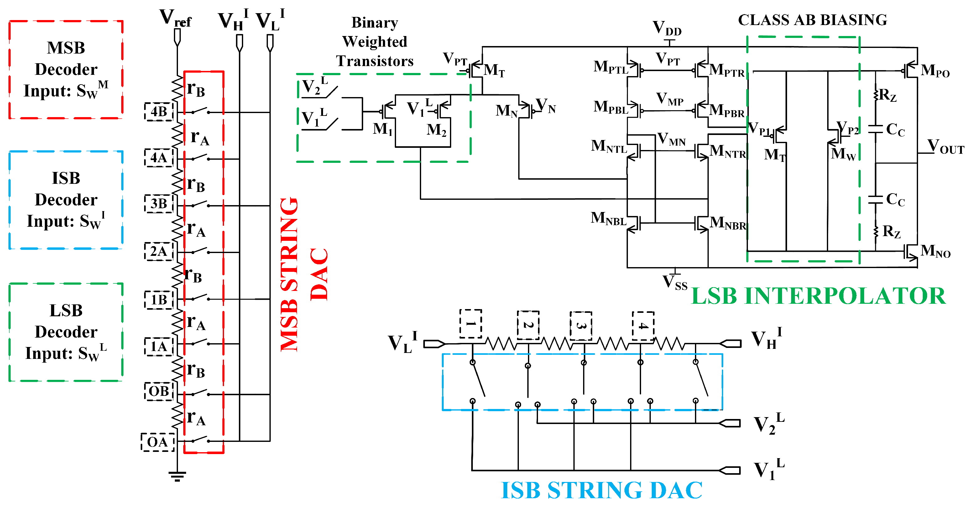
An n M -bit MSB subword of the digital input word is decoded to close two unique switches along the resistive string. A switch at node S w M connects to the first conductor to produce a voltage V 1 I , and a second switch at node S w M + 2 connects to a second conductor to produce a voltage V 2 I . The pair of voltages ( V 1 I , V 2 I ) serves as the high and low references for the subsequent ISB stage. The resistor string and the corresponding set of switches constitute the MSB string DAC, and the voltage pair is a coarse analog representation of the MSB subword. This coarse analog representation is intentionally non-monotonic. A key feature of this MSB switching method is the creation of negative jumps in the full DAC transfer curve, giving the converter a sub-radix characteristic. The result is a transfer function composed of 2 n M straight-line segments separated by these negative jumps, which occur whenever S w M changes. A total of 2 n M + 1 resistors are used in the MSB resistive string DAC if the MSB subword has n M bits. The schematic of the proposed MSB string DAC in context is presented in Figure 1 for an implementation where n M = 3 bits.

2.2.2. ISB String DAC

The proposed architecture also includes an Intermediate Significant Bit (ISB) string DAC. This stage performs an intermediate interpolation between the two reference voltages, V 1 I and V 2 I , provided by the MSB stage. This interpolation occurs in response to the n I -bit ISB subword. The schematic of the proposed ISB string DAC in context is presented in Figure 1 for an implementation where n I = 3 bits.

2.2.3. LSB Segment

The concept of an LSB differential pair interpolator was initially introduced in [13]. However, that work did not extend the idea to an interpolator that functions as a load-driving buffer. In our design, we implement a two-stage folded cascode amplifier with a Class AB biasing stage that serves as an interpolator and buffer for DAC output. The proposed architecture includes an n L -bit LSB segment which produces a fine interpolation between the reference voltages V 1 L and V 2 L provided by the ISB stage, wherein the interpolation occurs in response to an n L -bit LSB subword. The LSB segment is a two-stage cascode amplifier with a Class AB output stage, in which accuracy is assured by the precise summing of differential currents. This is accomplished by one of the amplifier’s PMOS input pairs being implemented as a binary-weighted transistor structure. The gates of the transistors within this structure are selectively connected to either V 1 L or V 2 L by switches, respectively, in response to the decoding of the n L -bit LSB subword. For an n L -bit LSB subword, the decoder is arranged so that each increment in the value of the subword switches the gate connection of a corresponding portion of the binary-weighted transistor structure, altering the effective transconductance of the differential pair. The output of the differential input pair drives the folded cascode stage, which provides high gain. The output of this first stage is then connected to a second stage, which includes the Class AB output buffer. The gate biases for the Class AB stage are provided by a Monticelli biasing circuit, which ensures stable rail-to-rail output performance. The amplifier’s input pair, implemented as a binary-weighted transistor structure, generates a differential signal current. This current is then processed by the folded cascode stage, and subsequently buffered by the Class AB stage to produce the final output voltage. This integrated design serves the dual purpose of being both an interpolator and the final output buffer. This integrated architecture eliminates the need for a separate buffer, reduces static loading on the ISB string, provides the necessary input common-mode range, and ensures rail-to-rail output performance to meet load requirements. The power consumption of the operational amplifier is 630 µW. Figure 2 provides a detailed circuit diagram of the proposed LSB interpolator for an implementation where n L = 2 bits.
Figure 3 shows the schematic of the proposed DAC design with an LSB differential pair interpolator connected in a unity feedback configuration.
The decoding scheme for the proposed DAC structure 1 is summarized in Table 1.
Under the assumption that the resistors and switches are ideal, the expressions for V 1 I and V 2 I are given below:
V 1 I = S w M D M 2 + E M × V REF
V 2 I = S w M + E M D M 2 + E M × V REF
where
E M = ( 2 ) D I 2 + D I
The ISB segment interpolates between the two voltages, V 1 I and V 2 I , provided by the MSB segment. Following this, the LSB segment performs a final interpolation between the two voltages, V 1 L and V 2 L , generated by the ISB. The expressions for V 1 L and V 2 L are shown below:
V 1 L = S w I D I ( V 2 I V 1 I ) + V 1 I
V 2 L = S w I + 1 D I ( V 2 I V 1 I ) + V 1 I
From the LSB interpolator, the DAC’s output is given below:
V out = S w L 2 n L ( V 2 L V 1 L ) + V 1 L
By substituting all the necessary parameters, we end up with the expression for V out given below:
V out = S w M · 2 n L · D I + ( S w L + 2 n L · S w I ) E M 2 n L · D I ( D M 2 + E M ) × V REF
Suppose that the target resolution post-calibration is n D A C ; then the expected step size is V L S B D = V REF 2 n D A C , and to attain good post-calibration linearity, n D A C < n , where n = n M + n I + n L . Consequently, for any change of 1 in the DAC code, S w , while the MSB code remains fixed, the change in output normalized to LSB is given below:
Δ V out V L S B D = E M ( 2 n D A C ) 2 n L · D I ( D M 2 + E M )
This equation captures the desired sub-radix and redundancy properties in the proposed architecture.

2.3. Improved Redundancy-Interpolated Three-Segment DAC

Simulation results for the proposed DAC structure 1 indicate that the proposed architecture exhibits a fundamental limitation in its post-calibration DNL at the target resolution of n D A C = n 1 . While simply lowering the target resolution ( n D A C ) improves the DNL metric, this approach presents an unfavorable trade-off between resolution and linearity. Analysis of the DAC’s transfer characteristic reveals that for a fixed MSB code, a single LSB step results in an output voltage change of approximately 0.92 LSB. To achieve superior DNL performance, this intra-segment step size must be reduced, thereby increasing the available redundancy for the calibration algorithm.
One effective method to reduce the step size is to decrease the effective resistance, E M , in the MSB string DAC where the ISB string connects. To accomplish this while preserving the essential sub-radix nature required for calibration, this effective resistance value must be constrained to be less than 2 r but greater than r. This is achieved in a modified architecture, referred to as DAC structure 2, by splitting each unit resistor r in the MSB string DAC into two parts, r A and r B . The relationship between these resistors is defined as
r A = γ r , r B = ( 1 γ ) r
where γ < 1 . The ISB and LSB string DACs remain unchanged. In this structure, for each MSB code, S w M , the high V 2 I and low V 1 I references of the ISB string DAC are connected to nodes, S w M ( A ) and S w M + 1 ( B ) , respectively, in the modified MSB string. A schematic of the improved structure is shown in Figure 4.
The corresponding decoding scheme for the proposed DAC structure 2 is summarized in Table 2.
Under the assumption that the resistors and switches are ideal, the output from the DAC can be expressed as
g m 1 S w L V 2 I + g m 1 ( 2 n L S w L ) V 1 I = g m 1 2 n L V out
g m 1 S w L ( V 2 I V 1 I ) + g m 1 2 n L V 1 I = g m 1 2 n L V out
V O U T ( S W ) = S w L 2 n L ( V 2 L V 1 L ) + V 1 L
where g m 1 is the transconductance of the LSB differential interpolator. Since the LSB is not a string DAC, there is no loading effect across the ISB. The ISB voltages can be expressed as
V 1 L = S w I D I ( V H I V L I ) + V L I
V 2 L = S w I + 1 D I ( V H I V L I ) + V L I
where D I is the total number of resistors in the ISB string DAC. Due to the loading effect of the ISB on the MSB string, the resistors in the MSB string across the ISB connection have their values altered. Taking that into consideration, the expressions for V H I and V L I are derived as
V H I = S w M ( 1 + γ ) + E m ( 2 n M 1 ) ( 1 + γ ) + E m V REF ,
V L I = S w M ( 1 + γ ) ( 2 n M 1 ) ( 1 + γ ) + E m V REF
where
E m = ( 2 γ + 1 ) D I 2 γ + D I + 1
Thus, the overall output voltage of the improved DAC architecture is given by
V OUT = S w L E m + 2 n L [ S w I E m + S w M ( 1 + γ ) ] 2 n L D I [ ( 2 n M 1 ) ( 1 + γ ) + E m ] V REF

3. Optimum Calibration (Binary Search Calibration)

The proposed optimum-chip calibration algorithm is as follows: For any desired post-calibration resolution n DAC , the INL of the n-bit DAC is first obtained pre-calibration. From the computed INL, the output of the DAC, V out , can be represented in the digital domain as V out LSB :
V out LSB ( S w ) = S w 2 n DAC 1 2 n 1 + INL ( S w )
A linear n DAC -bit DAC must generate 2 n DAC 1 unique voltages on a straight line. For this target resolution, the input code to the DAC is represented by C. For every C, the calibration scheme finds an S w that minimizes the error between C and V out LSB ( S w ) . The code C is then mapped to this optimal S w . This is performed for all C [ 0 , 2 n DAC 1 ] , thereby minimizing the post-calibration INL. The maximum of V out LSB is capped at 2 n DAC 1 . For a code C, the optimal S w which generates the desired output is obtained as shown in (20).
S w opt = arg min S w [ 0 , 2 n 1 ] V out LSB ( S w ) C
The optimization problem in (20) is solved via a binary search algorithm to obtain a mapping from C to S w opt . This requires an initial sorting of the V out LSB vector, which is a one-time cost [27,28]. The subsequent search for each C has a complexity of O ( n ) . The algorithm identifies which pre-calibration code ensures the desired linear response at the n D A C -bit level. This mapping is repeated across the full code space, and the resulting calibrated codes are stored for subsequent usage. This one-time calibration eliminates the need for repeated re-calibration, which offers an efficient and robust solution for integrated systems.

4. Implementation

The proposed DAC architectures are implemented in the TSMC 180 nm process with a 5-bit MSB, 5-bit ISB, and 6-bit LSB, giving a pre-calibration resolution of n = 16 . For both designs, each unit resistor is a 1 k Ω poly-resistor, ensuring a high level of matching while reducing area overhead. For DAC structure 2, a γ of 0.50 is chosen, setting both r A and r B to 500 Ω . This design sets the maximum post-calibration resolution, n DAC , to 15. Transmission gate switches are utilized in all string DACs. The decoders for the MSB and ISB stages are simple n-to- 2 n decoders. An external, ideal voltage source of 1.8 V is used to generate V REF .

5. Results

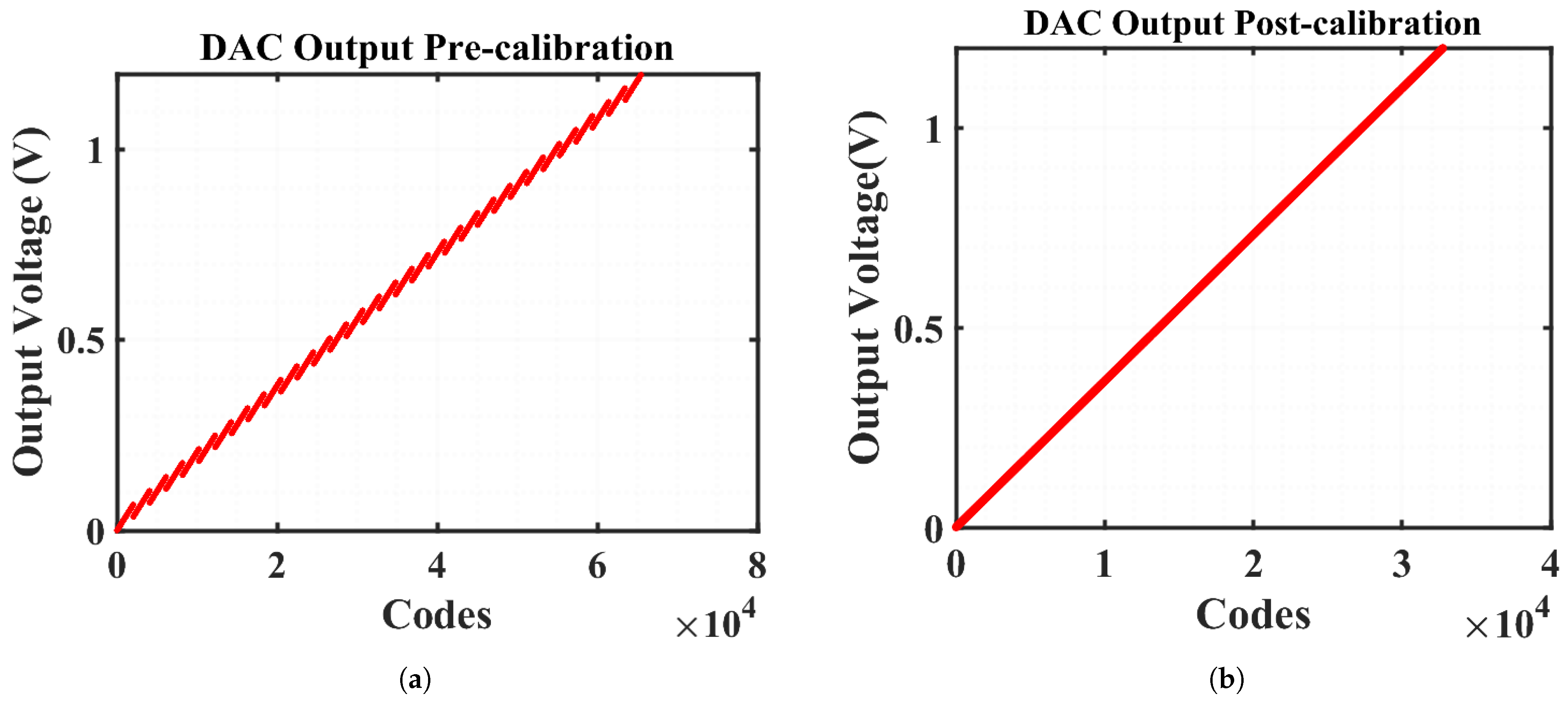
Simulations for both circuit designs were conducted in Cadence Spectre. To calibrate the design to a final resolution of n D A C = 15 , the binary search algorithm described above was implemented using MATLAB. The overall output characteristics for DAC structure 1 is illustrated in Figure 5, showing the transfer curve for the target resolution prior to and after calibration. The calibrated design achieved an INL of 0.48 LSB (14.54 ppm) and a DNL of 0.92 LSB (27.96 ppm). Figure 6 and Figure 7 provide a detailed comparison of the INL and DNL plots, both before and after calibration. Furthermore, the stability of the LSB differential pair interpolator is confirmed by a measured gain of 108 dB and a phase margin of 66°.
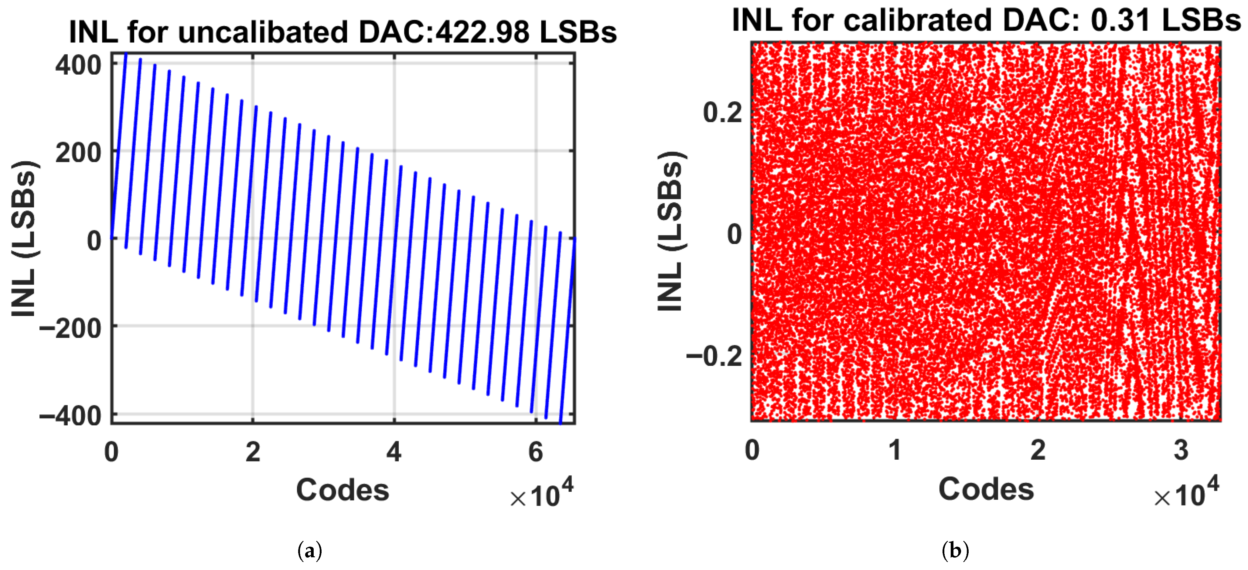
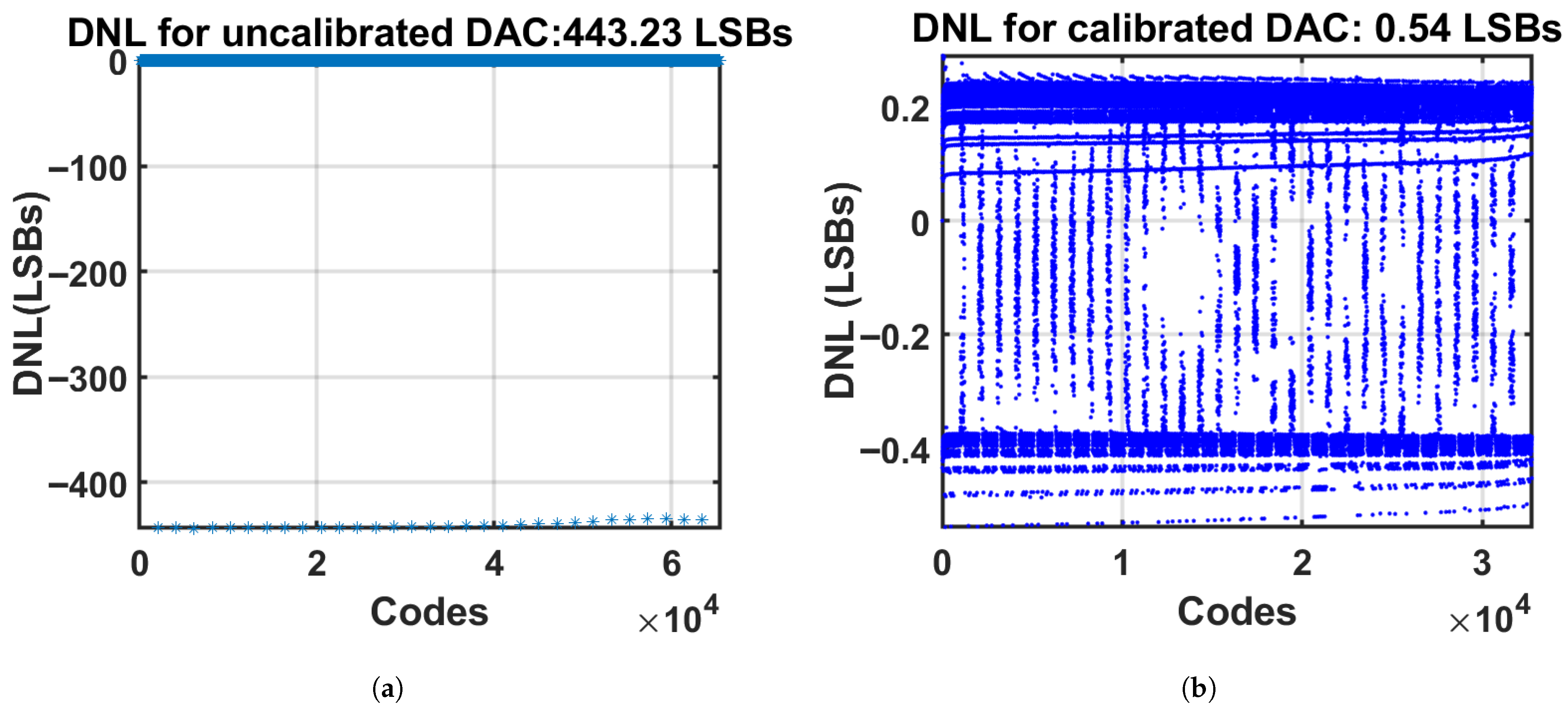
DAC structure 2 achieves a significant improvement in linearity over both DAC structure 1 and the architecture in [25] at the nominal and PVT (Process, Voltage, Temperature) corners. Simulation results at the nominal corner show a post-calibration INL of 0.31 LSB (9.51 ppm) and DNL of 0.54 LSB (16.43 ppm). A detailed comparison of the pre- and post-calibration INL and DNL plots is provided in Figure 8 and Figure 9, while the overall transfer curve for the target resolution is shown in Figure 10. The stability of the design is supported by the robust performance of its LSB differential pair interpolator, which exhibits a measured gain of 108 dB and a phase margin of 66°, as depicted in Figure 11.
To verify the robustness of DAC structure 2 against non-idealities, a Monte Carlo simulation was performed. A total of 100 Monte Carlo runs were conducted to assess the impact of both process and mismatch variations. The number of Monte Carlo runs was chosen to provide a fair comparison with the architecture proposed in [25]. In each simulation run, component values were varied randomly; this included not only the unit resistors but also transistor parameters such as width and length, which models variations in switch resistance and differential interpolator. The post-calibration linearity results for the target resolution are summarized in Figure 12. The analysis of the 100 iterations shows a worst-case INL of 0.48 LSB and a worst-case DNL of 0.68 LSB, confirming the architecture’s resilience to process and mismatch effects.
The probability density function (PDF) plots for INL and DNL are presented in Figure 13. The simulation yields a mean ( μ ) of 0.36 LSB and a standard deviation ( σ ) of 0.04 LSB for the maximum INL across 100 Monte Carlo runs. Similarly, the maximum DNL shows a mean of 0.48 LSB and a standard deviation of 0.11 LSB.
The dynamic performance of DAC structure 2 was evaluated through the spectral analysis of its output, both before and after calibration, as illustrated in the magnitude spectrum plots (Figure 14). The post-calibration spectrum demonstrates a substantial enhancement in signal integrity, characterized by a marked suppression of spurious tones and a significant reduction in harmonic distortion. This improvement is quantified by key performance metrics, with the Signal-to-Noise Ratio (SNR) increasing from 39.76 dB to 91.51 dB, the Spurious-Free Dynamic Range (SFDR) improving from 48.94 dB to 104.90 dB, the Signal-to-Noise and Distortion Ratio (SNDR) increasing from 39.11 dB to 91.48 dB, and the Total Harmonic Distortion (THD) reducing from 47.71 dB to 112.28 dB. Consequently, the Effective Number of Bits (ENOB) increased from 6.20 bits to 14.90 bits. These results underscore the efficacy of the proposed digital calibration algorithm in mitigating nonlinearities. The significant improvements across all measured dynamic performance metrics confirm that the calibration process not only enhances static linearity but also translates directly into a cleaner, more accurate analog output signal under dynamic conditions. The substantial increase in ENOB, in particular, validates the design’s ability to achieve high resolution.

6. Discussion

A data converter’s robustness against device mismatches and random manufacturing variations is primarily quantified by its static linearity metrics, namely, INL and DNL. For high-precision applications, achieving an INL below 0.5 LSB and a DNL of less than 1 LSB is a critical design target. The Monte Carlo simulation results confirm that our design comfortably meets these targets.
This represents a significant improvement over the prior state of the art. For instance, the architecture in [25] reported a worst-case post-calibration INL of 0.78 LSB and a DNL of 0.94 LSB for a 13-bit target resolution. An INL greater than 0.5 LSB can compromise a device’s effective resolution. Under the same post-calibration resolution, the proposed design achieves a worst-case INL of 0.24 LSB and a DNL of 0.38 LSB. This substantial enhancement is attributed to key architectural innovations.
A primary limitation in conventional segmented string DACs is the static loading that the LSB stage imposes on the preceding ISB string, which degrades DNL performance. The proposed architecture fundamentally overcomes this issue by implementing the LSB segment as an interpolating differential buffer. This approach eliminates any static loading from the LSB stage onto the ISB string DAC, directly contributing to the improved linearity. It is observed that the proposed design is comparable in terms of accuracy with other string DAC architectures present in the literature.
The proposed DAC structure 2 is compared to other interpolating string DAC designs from the literature, with a summary of the comparison provided in Table 3.

7. Conclusions

This paper introduces a 16-bit, three-segment string DAC that uses a redundancy-based architecture and on-chip digital calibration to enhance static linearity while minimizing area. The design’s key features include a split-resistor MSB stage, a redundancy-based ISB interpolator, and an LSB segment implemented with a folded-cascode amplifier that also serves as the output buffer. The design’s performance is validated through simulation, achieving post-calibration INL and DNL of less than ±1 LSB across process and mismatch variations. Subsequent work will focus on fabricating the design for empirical verification and characterization.

Author Contributions

Conceptualization, G.B. and I.B.; methodology, G.B.; software, G.B. and E.N.D.; validation, G.B., K.T. and E.N.D.; formal analysis, G.B.; investigation, G.B.; resources, D.C.; writing—original draft preparation, G.B.; writing—review and editing, K.T., I.B., E.N.D. and D.C.; supervision, D.C. All authors have read and agreed to the published version of the manuscript.

Funding

This work was supported by Semiconductor Research Corporation (Task No. 3160.012).

Data Availability Statement

No new data were created or analyzed in this study. Data sharing is not applicable to this article.

Conflicts of Interest

The authors declare no conflicts of interest.

References

  1. Toledo, P.; Rubino, R.; Musolino, F.; Crovetti, P. Re-Thinking Analog Integrated Circuits in Digital Terms: A New Design Concept for the IoT Era. IEEE Trans. Circuits Syst. II Express Briefs 2021, 68, 816–822. [Google Scholar] [CrossRef]
  2. Amankrah, E.; Geiger, R.; Tutuani, P. A Strategic Approach to Enhancing INL Performance in 10-Bit MOS-Based R-2R DACs through Area Allocation. In Proceedings of the IEEE National Aerospace and Electronics Conf. (NAECON), Dayton, OH, USA, 15–18 July 2024; pp. 163–167. [Google Scholar] [CrossRef]
  3. Mack, C.A. Fifty Years of Moore’s Law. IEEE Trans. Semicond. Manuf. 2011, 24, 202–207. [Google Scholar] [CrossRef]
  4. Beach, C.; Krachunov, S.; Pope, J.; Fafoutis, X.; Piechocki, R.J.; Craddock, I. An Ultra-Low-Power Personalizable Wrist-Worn ECG Monitor Integrated with IoT Infrastructure. IEEE Access 2018, 6, 44010–44021. [Google Scholar] [CrossRef]
  5. Yang, G.; Xie, L.; Mäntysalo, M.; Zhou, X.; Pang, Z.; Xu, L.D.; Kao-Walter, S.; Chen, Q. A Health-IoT Platform Based on the Integration of Intelligent Packaging, Unobtrusive Bio-Sensor, and Intelligent Medicine Box. IEEE Trans. Ind. Inform. 2014, 10, 2180–2191. [Google Scholar] [CrossRef]
  6. IEEE Innovation at Work. Make Batteries Last Longer: IEEE 802.11 Wake-Up Radio; IEEE: New York, NY, USA, 2017. [Google Scholar]
  7. Annema, A.-J.; Nauta, B.; van Langevelde, R.; Tuinhout, H. Analog Circuits in Ultra-Deep-Submicron CMOS. IEEE J. Solid-State Circuits 2005, 40, 132–143. [Google Scholar] [CrossRef]
  8. Murmann, B.; Nikaeen, P.; Connelly, D.J.; Dutton, R.W. Impact of Scaling on Analog Performance and Associated Modeling Needs. IEEE Trans. Electron. Devices 2006, 53, 2160–2167. [Google Scholar] [CrossRef]
  9. Maloberti, F. Data Converters; Springer: Dordrecht, The Netherlands, 2007. [Google Scholar] [CrossRef]
  10. Pelgrom, M. Analog-to-Digital Conversion; Springer: Cham, Switzerland, 2017. [Google Scholar] [CrossRef]
  11. Neidorff, R.A. Digital to Analog Converter Having Multiple Resistor Ladder Stages. U.S. Patent 5,554,986, 10 September 1996. Available online: https://patents.google.com/patent/US5554986A (accessed on 5 July 2025).
  12. Yenuchenko, M.S.; Pilipko, M.M.; Morozov, D.V. A 10-bit Segmented M-String DAC. In Proceedings of the 2018 IEEE Conference of Russian Young Researchers in Electrical and Electronic Engineering (EIConRus), Moscow, Russia, 29–31 January 2018; pp. 265–268. [Google Scholar] [CrossRef]
  13. Remper, W.C. Digital to Analog Converter. U.S. Patent 5,396,245, 7 May 1995. Available online: https://patents.google.com/patent/US5396245A (accessed on 5 July 2025).
  14. Basic DAC Architectures III: Segmented DACs by Walt Kester. Available online: https://www.analog.com/media/en/training-seminars/tutorials/MT-016.pdf (accessed on 27 August 2025).
  15. Sarkar, S.; Banerjee, S. A 10-Bit 500 MSPS Segmented DAC with Optimized Current Sources to Avoid Mismatch Effect. In Proceedings of the 2015 IEEE Computer Society Annual Symposium on VLSI, Montpellier, France, 8–10 July 2015; pp. 172–177. [Google Scholar] [CrossRef]
  16. Alvarez-Fontecilla, E.; Wilkins, P.S.; Rose, S.C. Understanding High-Resolution Dynamic Element Matching DACs. IEEE Circuits Syst. Mag. 2024, 23, 34–43. [Google Scholar] [CrossRef]
  17. Chang, K.-H.; Hsieh, C.-C. A 12-bit 150-MS/s Sub-Radix-3 SAR ADC with Switching Miller Capacitance Reduction. J. Solid-State Circuits 2018, 53, 1755–1764. [Google Scholar] [CrossRef]
  18. Baker, R.J. CMOS Circuit Design, Layout, and Simulation, 3rd ed.; Wiley-IEEE Press: Hoboken, NJ, USA, 2010; Available online: https://www.wiley.com/en-us/-p-9780470891179 (accessed on 12 July 2025).
  19. Gagliardi, F.; Dei, M. Accuracy Enhancement of Resistor-String Digital-to-Analog Converters through Averaging Dynamic Element Matching. In Proceedings of the 2025 IEEE 28th International Symposium on Design and Diagnostics of Electronic Circuits and Systems (DDECS), Lyon, France, 5–7 May 2025; pp. 74–79. [Google Scholar]
  20. IEEE Std 1658-2023; IEEE Standard for Terminology and Test Methods of Digital-to-Analog Converter Devices. IEEE: Piscataway, NJ, USA, 2023. [CrossRef]
  21. Cong, C.; Geiger, R.L. Formulation of INL and DNL yield estimation in current-steering D/A converters. In Proceedings of the 2002 IEEE International Symposium on Circuits and Systems (ISCAS), Phoenix-Scottsdale, AZ, USA, 26–29 May 2002; p. III. [Google Scholar]
  22. Ting, H.-W.; Wu, Z.-T.; Yan, J.-Z.; Wu, H.-Y. A Segmented Resistor-String DAC-Based Stimulus Generator for ADC Linearity Testing. In Proceedings of the 2018 International Symposium on Next-Generation Electronics (ISNE), Hsinchu, Taiwan, 7–9 May 2018; pp. 1–4. [Google Scholar] [CrossRef]
  23. Liu, N.; Todsen, J.; Chen, D. An 8-bit Low-Cost String DAC with Gradient-Error Suppression to Achieve 16-bit Linearity. IEEE Trans. Circuits Syst. I Regul. Pap. 2020, 67, 2157–2168. [Google Scholar] [CrossRef]
  24. Wen, M.K.K.; Ahmad, N.b.; Yusoff, Y.b.; Majid, H.A. Design of a 14-bit Hybrid DAC for High Resolution Applications in SAR ADCs. In Proceedings of the 6th IEEE International Conference on Recent Advances and Innovations in Engineering (ICRAIE), Kedah, Malaysia, 1–3 December 2021; pp. 1–6. [Google Scholar]
  25. Bruce, I.; Darko, E.N.; Odion, E.O.; Crabb, M.; Chen, D. Redundancy-Based Resistor-String DAC with an All-Digital Calibration Algorithm. In Proceedings of the 2024 IEEE 67th International Midwest Symposium on Circuits and Systems (MWSCAS), Springfield, MA, USA, 4–7 August 2024; pp. 571–575. [Google Scholar] [CrossRef]
  26. Dempsey, D. Digital to Analog Converter. U.S. Patent 5,969,657, 22 July 1997. Available online: https://patents.google.com/patent/US5969657A/en (accessed on 5 July 2025).
  27. Binary Search Algorithm. Wikipedia. 1 June 2024. Available online: https://en.wikipedia.org/w/index.php?title=Binary_search_algorithm&oldid=1226792725 (accessed on 6 June 2025).
  28. Cormen, T.H.; Leiserson, C.E.; Rivest, R.L.; Stein, C. Introduction to Algorithms, 4th ed.; MIT Press: Cambridge, MA, USA, 2022. [Google Scholar]
  29. Parthasarathy, T.; Kuyel, T.; Yu, Z.; Chen, D.; Geiger, R. A 16-bit resistor string DAC with full-calibration at final test. In Proceedings of the IEEE International Test Conference, Austin, TX, USA, 8 November 2005. [Google Scholar] [CrossRef]
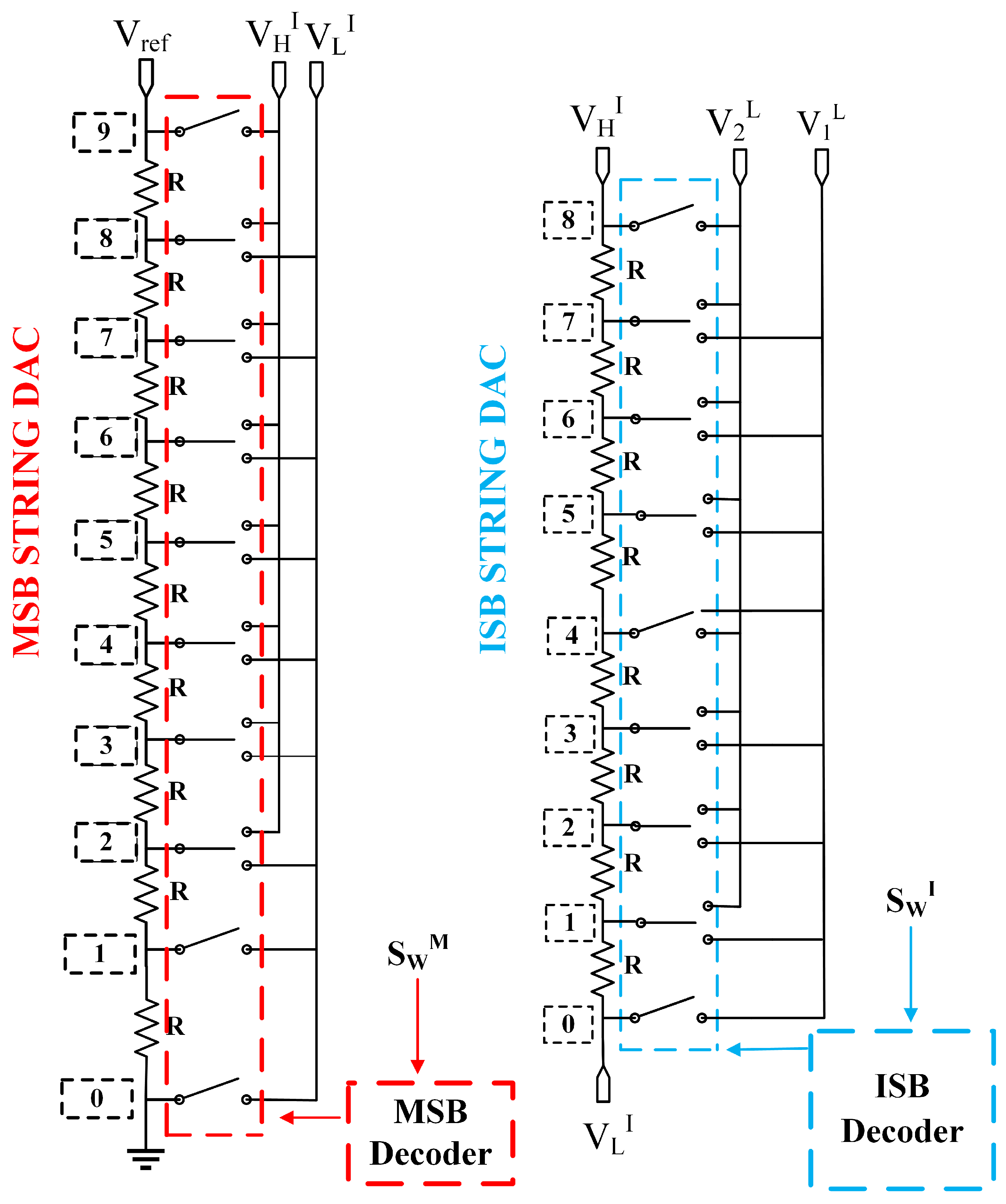
Figure 1. Implementation of MSB and ISB string DACs for n I = n M = 3 bits.
Electronics 14 03477 g001
Figure 2. Implementation of proposed differential interpolator for n L = 2 .
Electronics 14 03477 g002
Figure 3. Schematic of the proposed DAC design, with its LSB differential pair interpolator configured for unity feedback.
Electronics 14 03477 g003
Figure 4. Schematic of improved DAC structure for n M = n I = n L = 2 bits.
Electronics 14 03477 g004
Figure 5. (a) Pre-calibration DAC transfer curve for DAC structure 1. (b) Post-calibration DAC transfer curve for DAC structure 1.
Electronics 14 03477 g005
Figure 6. (a) Pre-calibration INL characteristics at the nominal corner for DAC structure 1. (b) Post-calibration INL characteristics at the nominal corner for DAC structure 1.
Electronics 14 03477 g006
Figure 7. (a) Pre-calibration DNL characteristics at the nominal corner for DAC structure 1. (b) Post-calibration DNL characteristics at the nominal corner for DAC structure 1.
Electronics 14 03477 g007
Figure 8. (a) Pre-calibration INL characteristics at the nominal corner for DAC structure 2. (b) Post-calibration INL characteristics at the nominal corner for DAC structure 2.
Electronics 14 03477 g008
Figure 9. (a) Pre-calibration DNL characteristics at the nominal corner for DAC structure 2. (b) Post-calibration DNL characteristics at the nominal corner for DAC structure 2.
Electronics 14 03477 g009
Figure 10. (a) Pre-calibration DAC transfer curve for DAC structure 2. (b) Post-calibration DAC transfer curve for DAC structure 2.
Electronics 14 03477 g010
Figure 11. Gain and phase margin plots at the nominal corner.
Electronics 14 03477 g011
Figure 12. (a) Post-calibration INL across 100 different Monte Carlo simulations. (b) Post-calibration DNL across 100 different Monte Carlo simulations.
Electronics 14 03477 g012
Figure 13. (a) Maximum INL for 100 MC runs. (b) Maximum DNL for 100 MC runs.
Electronics 14 03477 g013
Figure 14. (a) Magnitude spectrum of the uncalibrated DAC output for DAC structure 2. (b) Magnitude spectrum of the calibrated DAC output for DAC structure 2.
Electronics 14 03477 g014
Table 1. Summary of decoding scheme employed in proposed DAC structure 1.
Voltage (V)Node NumberSegmented DACs
V 2 I S w M + 2 MSB
V 1 I S w M MSB
V 2 L S w I + 1 ISB
V 1 L S w I ISB
V out S w I is even: S w L LSB
S w I is odd: 2 n L 1 S w L LSB
Table 2. Summary of decoding scheme employed in proposed DAC structure 2.
Voltage (V)Node NumberSegmented DACs
V 2 I S w M + 1 ( B ) MSB
V 1 I S w M ( A ) MSB
V 2 L S w I + 1 ISB
V 1 L S w I ISB
V out S w I is even: S w L LSB
S w I is odd: 2 n L 1 S w L LSB
Table 3. Comparison of the proposed design with the existing literature.
ParameterElConRus [12]ITC [29]TCAS-1 [23]MWSCAS [25]This Work
Technology (µm)0.180.50.130.180.18
Resistor MaterialPolyTaNPolyPoly
ArchitectureSegmented
string DAC
String DAC +
calibration DAC
String DAC +
interpolating
amplifier
Segmented
string DAC
String DAC +
differential
interpolator
Resolution (bits)101681315
Output range (V)1.853.31.21.2
INL (ppm/LSB)9k/9.4122/7.9921/5.37m95/0.7816/0.48
DNL (ppm/LSB)273/0.286.1/0.4918/4.61m124/0.9421/0.68
MeasurementNoYesYesNoNo
Disclaimer/Publisher’s Note: The statements, opinions and data contained in all publications are solely those of the individual author(s) and contributor(s) and not of MDPI and/or the editor(s). MDPI and/or the editor(s) disclaim responsibility for any injury to people or property resulting from any ideas, methods, instructions or products referred to in the content.