Article

High-Density Neuromorphic Inference Platform (HDNIP) with 10 Million Neurons

1
The State Key Laboratory of Electronic Thin Films and Integrated Devices, University of Electronic Science and Technology of China, Chengdu 610054, China
2
The Shenzhen Institute for Advanced Study, University of Electronic Science and Technology of China, Shenzhen 518110, China
*
Author to whom correspondence should be addressed.
Electronics 2025, 14(17), 3412; https://doi.org/10.3390/electronics14173412
Submission received: 14 July 2025 / Revised: 13 August 2025 / Accepted: 19 August 2025 / Published: 27 August 2025
(This article belongs to the Special Issue Feature Papers in Artificial Intelligence)

Abstract

Modern neuromorphic processors exhibit neuron densities that are orders of magnitude lower than those of the biological cortex, hindering the deployment of large-scale spiking neural networks (SNNs) on single chips. To bridge this gap, we propose HDNIP, a 40 nm high-density neuromorphic inference platform with a density-first architecture. By eliminating area-intensive on-chip SRAM and using 1280 compact cores with a time-division multiplexing factor of up to 8192, HDNIP integrates 10 million neurons and 80 billion synapses within a 44.39 mm 2 synthesized area. This achieves an unprecedented neuron density of 225 k neurons/ mm 2 , over 100 times greater than prior art. The resulting bandwidth challenges are mitigated by a ReRAM-based near-memory computation strategy combined with input reuse, reducing off-chip data transfer by approximately 95%. Furthermore, adaptive TDM and dynamic core fusion ensure high hardware utilization across diverse network topologies. Emulator-based validation using large SNNs, demonstrates a throughput of 13 GSOP/s at a low power consumption of 146 mW. HDNIP establishes a scalable pathway towards single-chip, low-SWaP neuromorphic systems for complex edge intelligence applications.

1. Introduction

Neuromorphic computing, drawing inspiration from the remarkable efficiency of the biological brain, holds immense promise for developing low-power intelligent systems [1]. Significant achievements have progressively shaped the neuromorphic ecosystem [2,3,4,5]. However, realizing this promise for large-scale, bio-inspired spiking neural networks (SNNs) presents unique and formidable architectural demands.
Conventional high-performance architectures, such as GPUs and TPUs [6,7], while offering high theoretical performance through extensive parallel arithmetic units, are fundamentally mismatched with SNN characteristics. Their general-purpose nature is ill-suited for 1-bit sparse spike processing, leading to considerable overhead and energy efficiency [8]. Even specialized SNN accelerators, often composed of fewer, larger cores [9,10,11,12], encounter substantial challenges when mapping cortical-scale networks [13]. These networks, typically comprising millions to tens of billions of neurons and billions to trillions of synapses, necessitate distributing neurons and synapses across limited processing units or memory blocks, thereby incurring significant data movement overhead from inter-neuronal communication. This constraint restricts the integration of large-scale parallel processing units, which are indispensable for accurately simulating the inherent parallelism of biologically faithful models or realizing cortical-scale computation [14,15].
A critical factor for emulating the massive intrinsic parallelism of SNNs in near-real-time is achieving a comparable level of hardware parallelism. Biological systems, such as the human cerebral cortex (16–23 billion neurons over ∼1800 cm 2 ), exhibit remarkable computational power within a compact volume, boasting neuron densities around 100 k neurons/ mm 2 [16,17,18]. In stark contrast, current state-of-the-art neuromorphic VLSI chips are severely constrained by low areal density. For instance, IBM’s TrueNorth [19,20] integrated 1 million neurons on a large 430 mm 2 die (28 nm), limiting cost-effectiveness. Intel’s Loihi series [21,22,23], while improving integration (Loihi-2: 1 M neurons, 31 mm 2 , Intel 4), incorporated complex features like on-chip learning, which added area overhead and constrained pure computational density for inference-focused designs. Other platforms also highlight this density constraint, from custom ASICs like Tianjic [24,25] (39 k neurons, 14.44 mm2, 28 nm) and MorphIC [26] (2 k neurons, 65 nm), to architectures with different design goals. For instance, the asynchronous mixed-signal DYNAP-SE2 [27] processor prioritizes biological fidelity, implementing 1024 physical neurons on a 98 mm 2 chip (180 nm), while flexible FPGA platforms like SNAVA [28] are designed for research reconfigurability rather than optimized density. Consequently, existing digital neuromorphic chips have largely stagnated around an effective density of approximately 1 k virtual neurons/ mm 2 at 40 nm, creating a significant gap compared to their biological counterparts.
Consequently, digital neuromorphic chips have largely stagnated around an effective density of approximately 1 k virtual neurons/ mm 2 at 40 nm, a two-orders-of-magnitude gap compared to biological counterparts. This low integration density means that attempting to model cortical-scale networks [13,16,17,18] or advanced AI models like large-scale spiking Transformers [29,30] on such platforms would necessitate hundreds of chips, leading to impractical systems crippled by inter-chip communication bottlenecks. Conversely, densities exceeding 100 k neurons/ mm 2 could enable their integration onto a single die or a few chiplets, making large-scale deployment feasible, especially for size-, weight-, and power-constrained (SWaP) edge applications [31,32,33,34,35]. Boosting on-chip neuron density is, therefore, the foremost challenge for scalable and impactful neuromorphic hardware [36].
Achieving densities approaching the 100 k neurons/ mm 2 baseline necessitates radical architectural shifts, primarily the elimination of area-hungry on-chip SRAM for weights, a component known for poor scaling in advanced nodes (e.g., TSMC 7-3nm [37,38,39]) and a primary density limiter in prior designs. Furthermore, aggressive time-division multiplexing (TDM) is often employed to increase virtual neuron count. However, these strategies introduce significant new VLSI challenges: (1) Static TDM, while increasing virtual neuron capacity, often suffers from poor hardware utilization when mapping diverse network structures, thereby diluting effective density gains, as observed in our previous work [40] where large networks could not be deployed efficiently, and small networks led to idle hardware. (2) Removing SRAM storage shifts a massive data traffic burden to package pins, creating an external-bandwidth wall, inflating I/O energy, and throttling throughput. While any accelerator can support many virtual neurons given sufficient external memory, doing so typically incurs substantial energy and latency penalties for frequent off-chip data access.
This work is an extension of our previous conference work [41], which primarily introduced the structural design and feasibility experiments of HDNIP’s flexible network computing. To address these fundamental issues, we introduce HDNIP, a 40 nm high-density neuromorphic inference platform architecture. HDNIP differs by maximizing the physical density of computational cores on-chip. It integrates 80 flexible-core clusters (FCCs), comprising 1280 parallel cores, capable of hosting up to 10 million neurons and 80 billion synapses within a single die. Our contributions are as follows:
(1) Density-First Architecture: We prioritize computational density by eliminating on-chip weight SRAM, employing a highly reusable core, achieving a synthesis estimated at 225 k neurons/ mm 2 (synthesized at 40 nm).
(2) Adaptive Utilization Enhancement: We improved hardware utilization across diverse network topologies compared to static schemes through adaptive TDM and dynamic core fusion, approaching significantly high utilization.
(3) Bandwidth Wall Mitigation: We introduce a ReRAM-based near-memory computing (NMC) strategy for off-chip weight storage, drastically cutting weight bandwidth needs (∼80%). A 4-input-reuse scheme was implemented to achieve a 4-times reduction in input bandwidth, resulting in an overall bandwidth reduction of ∼95%. Moreover, the multi-lane interface was optimized to enhance data transmission and facilitate system scalability.
(4) System Validation: We demonstrated capabilities via FPGA emulation and synthesis, achieving 13.64 GSOP/s average throughput for large SNNs at a projected 146 mW, including ReRAM estimates.
In summary, HDNIP addresses the critical limitations of low neuron density, on-chip SRAM bottlenecks, TDM inefficiency, and the external memory bandwidth wall that have constrained previous neuromorphic processors, aiming to provide a promising, scalable path towards monolithic cortex-scale neuromorphic systems.
The remainder of this paper is organized as follows. Section 2 details the proposed HDNIP architecture and its enabling circuit techniques. Section 3 presents the evaluation results. Section 4 concludes and discusses the paper.

2. HDNIP’s Architecture

To meet the computational density and throughput requirements for large-scale SNN inference, the overall organizational structure and key modules of the HDNIP architecture have been devised, as illustrated in Figure 1. Without advancing the process node, the architecture achieves large-scale integration of neurons and synapses through a series of density-oriented design strategies. This section delineates HDNIP’s architectural details from four perspectives: the overall design philosophy, high-density core array, bandwidth optimization strategy, and a simplified cluster-based communication scheme.

2.1. Overall Organization and Design Philosophy

The overall structure provides the foundation for achieving high computational density, primarily realized through the innovative core design discussed next. The overall architecture of HDNIP is constructed around expanding the core array and simplifying the on-chip support logic. The chip has an extensive parallel core array comprising 1280 configurable computation cores distributed across 80 FCCs, each cluster containing 16 cores. This computation core cluster array enables support for up to 10 million neurons and 80 billion synaptic connections on a single chip, thereby substantially enhancing computational density to a scale approaching biological neural systems. The cores are integrated in a tightly packed arrangement to maximize computational functionality per unit area.
Moreover, to obviate the need for fine-grained independent control of each core, which would incur additional control overhead and circuit complexity, a cluster-level organizational approach is adopted, whereby every 16 cores are grouped into an FCC managed by a unified controller (UC). This grouping retains the essential core functionalities and communication capabilities while effectively reducing resource overhead related to control and power management, thereby realizing an efficient clustered organizational structure.
Surrounding the core array, HDNIP incorporates a series of lightweight on-chip peripheral modules to provide data transmission and configuration management support. The primary modules include a multi-lane interface for high-speed data input; a configuration controller responsible for global configuration control; a data packet module (DPM) for input data distribution and sequence synchronization; two transmission modules that employ temporary registers for buffering intermediate data and weights; and a serial-to-parallel conversion module (S2P) dedicated to retrieving weight data from external storage. These peripheral modules operate in concert to efficiently interface external storage and transport resources with the internal core array.
Regarding clock design, HDNIP is partitioned into three mutually independent clock domains to balance performance and power consumption across different functional modules: a high-speed computational clock domain drives the core array for neuronal computations; a moderate-frequency, flexibly scalable interface clock domain facilitates chip-to-external communication; and a low-speed non-volatile memory (NVM) clock domain is dedicated to the read and write operations of weight storage devices such as ReRAM. This multi-clock domain design guarantees that each circuit component functions at optimal frequency, minimizing unnecessary power consumption and enhancing overall efficiency.
Importantly, this multi-core architecture, built on configurable cores and organized into FCCs, supports seamless expansion, allowing additional clusters to be integrated with minimal complexity to scale the system further. Although current hardware simulation constraints limit scaling to higher levels, advancements in future process technology and design methodologies are expected to enable chips with even larger neuron scales, ultimately facilitating full cortical simulation.
Thus, through these comprehensive organizational choices and design trade-offs, encompassing the large-scale clustered core array, lightweight peripheral support, and optimized multi-domain clocking, HDNIP establishes the foundational framework necessary for achieving ultra-high computational density. Building upon this robust foundation, the innovative design and optimization of the core computational units become critical for fully realizing this density and enhancing overall efficiency, as elaborated in the following.

2.2. High-Density-Oriented Versatile Core Design

To maximize the integration of neurons and synapses within the limited silicon area, each HDNIP core minimizes logic and storage overhead. Increasing the TDM factor, although yielding a higher neuron density, reduces deployment flexibility and performance degradation. This section delineates the realization of variable TDM through a compact core implementation and the adoption of cluster sharing to enhance deployment versatility.

2.2.1. Compact Core Design

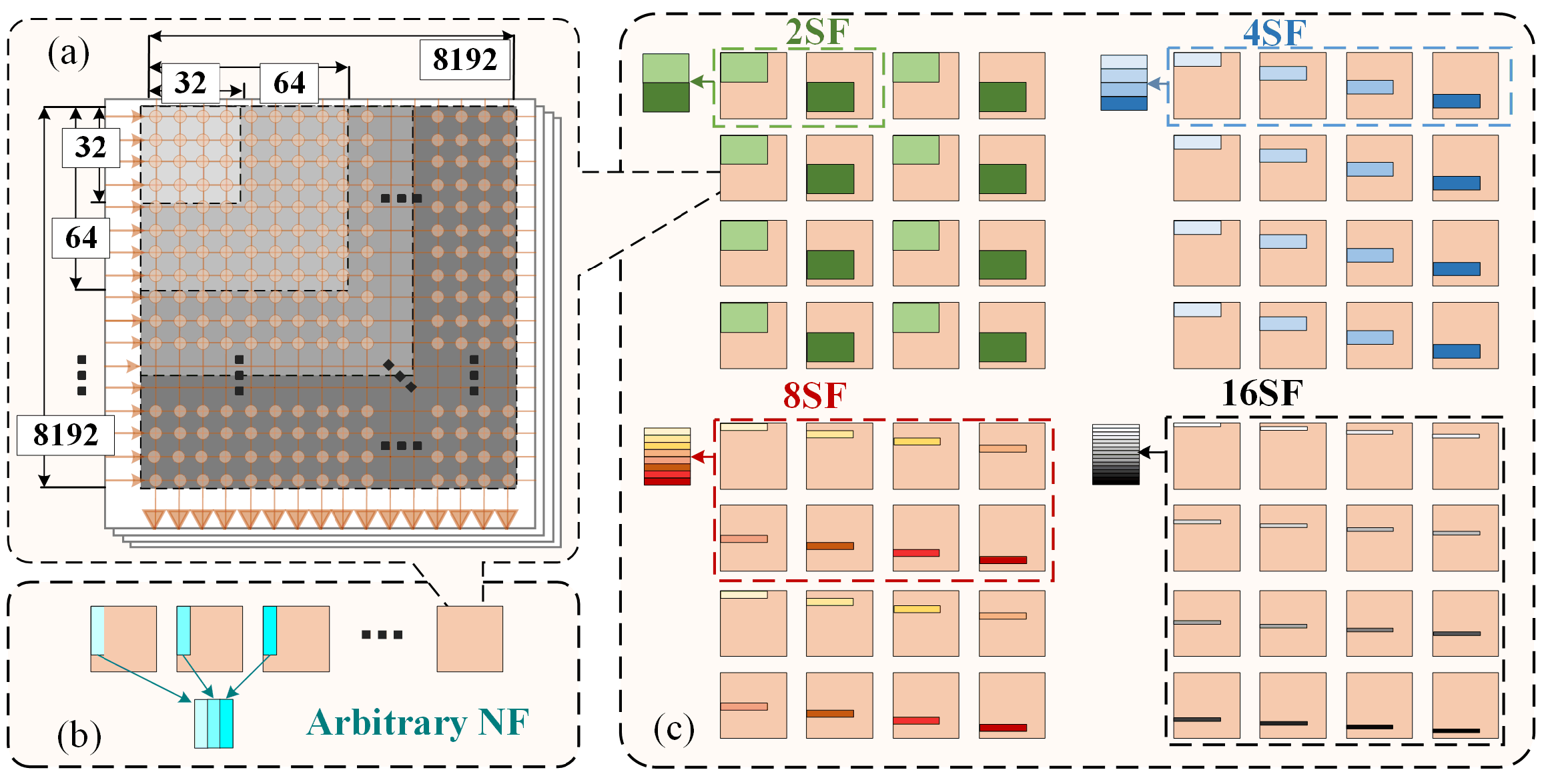
The 1280 computation cores are divided into 80 core clusters to simplify the scale of hardware control circuits, reduce costs, and lower overhead. As shown in Figure 2a, each flexible core cluster contains 16 cores with consistent virtual neuron array sizes and is controlled by a unified configuration module for the cluster.
Figure 2b shows the circuit design of the compact core, which includes the synapse unit, dendrite unit, and soma unit. In the synapse unit, a weight-sharing method is used. A 4-bit weight state is obtained from outside the core, and the corresponding 16-bit weight data are retrieved from the internal lookup table for computation. TDM saves area overhead in the dendrite unit, where one of the four membrane potentials is accumulated per input data. In the soma unit, leakage, reset, and output generation are performed. The input buffer holds 1-bit values, which, after undergoing accumulation with 16-bit weights, produce a 16-bit accumulated value. Following activation by the soma unit, the output remains a 1-bit value.
The most popular LIF neuron model is implemented, as shown in the following:
M P t = M P t 1 + W l ( D ) S t 1 S t = H ( M P t )
where W l is a weight lookup table (LUT), and when the weight state variable D is inputted, the output weight is calculated. H ( x ) is a step function: if x is less than 0, no spike is fired; otherwise, a spike is fired. The input buffer in Figure 2b stores spikes. In the dendrite unit, the inverter for weights is disabled, and after the membrane potential calculation, the soma structure in the LIF neuron fires spikes and outputs the membrane potential.

2.2.2. Adaptive Time-Division Multiplexing

Compact cores employ a high-TDM technique in the dendrite unit. Each physical core is time-multiplexed to emulate a virtual neuron–synapse crossbar array that substantially exceeds its inherent hardware scale. In other words, a compact physical core can sequentially compute state updates for neurons over rapid, consecutive temporal segments, effectively expanding the compact core into a large-scale crossbar array. This mechanism facilitates an order-of-magnitude increase in neuron/synapse density, establishing the basis for the architecture’s high density.
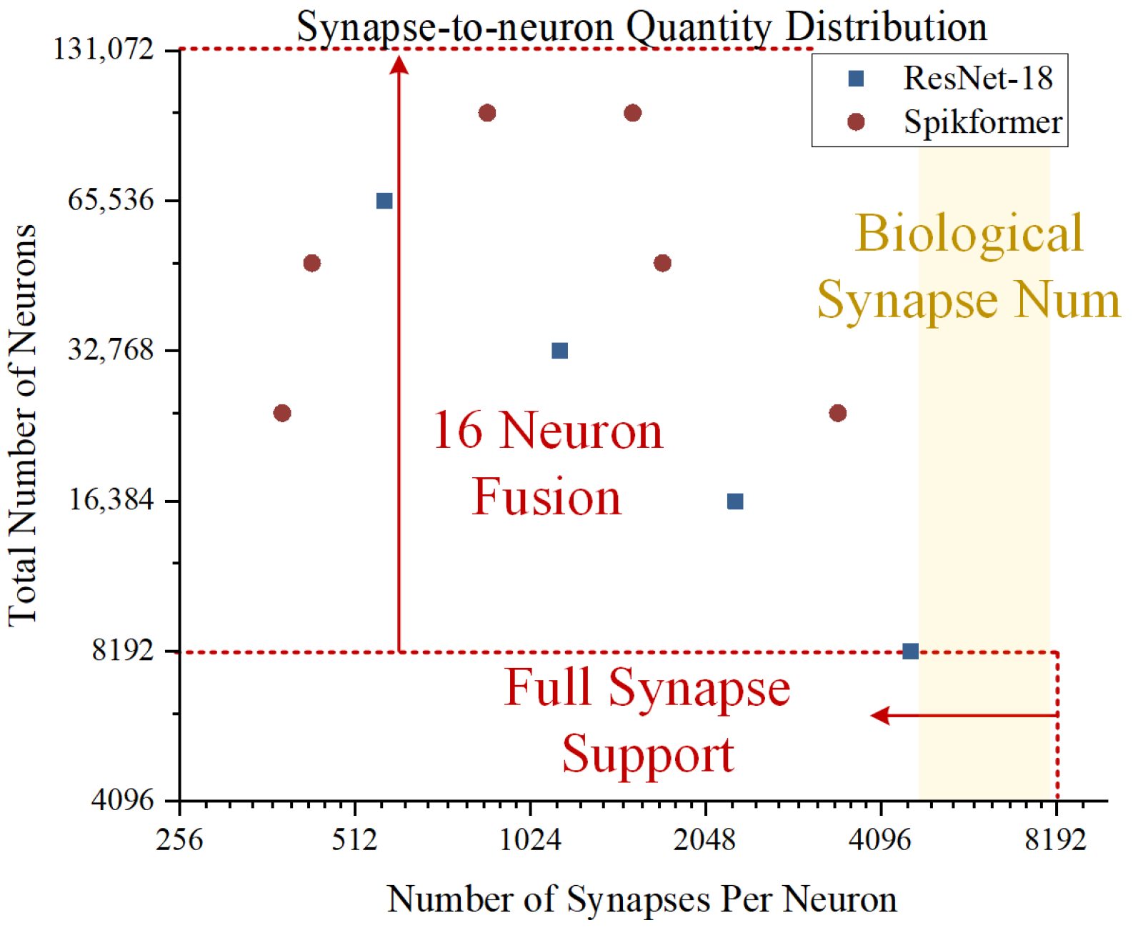
For medium-to-large-scale networks [29,42], as shown in Figure 3, the number of required synapses typically exceeds 4096, and neurons surpass 8192. By configuring the crossbar scale appropriately, our design better approximates the connectivity observed in the human brain, where each neuron typically connects to 5000–8000 synapses [43]. Our configuration supports up to 8192 neurons per core, allowing the output of one core to serve directly as the synaptic input for the next, which enhances inter-core connectivity.
To improve the flexible deployment capability of high-density computation, the cores within the flexible core cluster support a variable-scale virtual crossbar structure. As shown in Figure 4a, the core can simulate 32–8192 synapses and neurons, and they can be freely combined to form virtual crossbar computation arrays that match the scale of the network mapping. The TDM ratio of each core is not fixed but can be configured before runtime to suit the scale of the targeted neural network layer. When a layer requires a relatively small number of neurons and synapses to be emulated, the number of TDM cycles is reduced to minimize idle overhead; conversely, when the layer’s scale approaches the core’s maximum capacity, the hardware is fully exploited. Consequently, network layers of varying scales can be executed on a single core with nearly 100% utilization, avoiding resource underutilization inherent in fixed TDM configurations.

2.2.3. Shared Core Fusion

For large network layers that exceed the capacity of a single core, or for small network layers where parallel core computation is desired to reduce latency, HDNIP permits the fusion of multiple cores in the FCC into a single logical computing unit to collaboratively execute the layer’s computation. The FCC supports both neuron and synapse splitting and inherently supports neuron-level fusion. The SCF module also supports synapse-level fusion.
Neuron-level fusion (NF), as shown in Figure 4b, is expressed as follows:
M P = M P + W M × N X N = M P + [ W m × N X N , , W m × N X N k ]
where m = M / k . The complete weight matrix is split into k blocks from the output direction, with each block sized m × N , and k supports arbitrary sizes. Since the computation core outputs data only after completing the neuron calculations, the output data are integrated and fused externally without requiring support from the SCF module. As shown on the left of Figure 2c), the soma unit inside the core operates normally, and after bypassing the SCF module, the data are directly output.
For synapse-level fusion, the situation becomes much more complex:
M P = M P + W M × N X N = M P + k W M × n X n
where n = N / k . The complete weight matrix is split into k blocks from the input direction, with each block sized M × n . Since synapse fusion requires summing the partial results from each core, only a limited number of synapse fusions are supported, as shown in Figure 4c. Synapse fusion cannot support arbitrary scales, and all cores must participate in the fusion process to simplify circuit control. For example, in a 4-neuron core fusion, the results of every 4 cores are fused and output. The summation of partial results and the new output spike generation are integrated into the SCF module. At this point, the soma inside the core ceases operation.
Figure 2c shows the circuit design details of the shared core fusion module. Since the output bandwidth is significantly 32–8192-times lower than the input bandwidth, considering the compact design, the SCF module with pipeline structure is shared among the 80 FCCs. Within the module, to achieve the accumulation and summation of partial results for various types of synapse fusion, an array of 32 adders is constructed. The buffer registers’ design allows for the reuse to implement the addition trees of different scales. In SF mode, the core shown in Figure 2b only outputs partial results, while the result is generated within the SCF. Therefore, an additional shared soma (SS) unit must be incorporated into the module to ensure the correct output of the result.
The decision to share the SCF module across 80 FCCs is a deliberate design choice aimed at maximizing area efficiency without compromising performance at the target scale. This approach is justified for three main reasons. First, the core’s output bandwidth is 32–8192-times lower than its input bandwidth, making a single pipelined SCF capable of handling the reduced data flow from all clusters. Second, synapse-level fusion is a specialized operation; having dedicated SCFs for each cluster would result in significant idle hardware and unnecessary area overhead, which contradicts our high-density goal. Finally, while this shared resource could pose a bottleneck in vastly larger systems, our extensive validations confirm that for the 10-million-neuron scale, the SCF does not limit the overall performance, even when deploying large and complex networks.
In summary, the high-density core array of HDNIP, in conjunction with configurable TDM and core fusion techniques, ensures a high neuron integration density per unit area and fully utilizes computational resources through adaptation to varying task scales. Experimental results presented in Section 3 further substantiate deploying a practical large-scale SNN. Compared to conventional fixed TDM, our architecture allows for extremely high utilization, and resource efficiency was further optimized via core fusion, thereby reducing overall latency.

2.3. Bandwidth Optimization Strategy

In pursuit of extremely high density by removing on-chip weight SRAM, HDNIP employs a multifaceted bandwidth optimization strategy to preclude external data transfers from emerging as a system bottleneck.

2.3.1. General Compact-Weight Near-Memory Computing

In large-scale, high-density neuromorphic computing at the 10 M scale, the bandwidth overhead of computation cores is significant. Figure 5a shows the bandwidth proportions of different data types, where the weight overhead far exceeds that of input and MP data. Caching weights can significantly alleviate external bandwidth pressure, enabling near-memory computing and improving computation core utilization.
Non-volatile memory has seen rapid development over the past decade. Figure 5b demonstrates that NVMs significantly outperform SRAM in density, which is advantageous for large-scale neuromorphic computing [44,45,46]. The differences among various NVM types also determine their different applications, but all NVMs generally suffer from lower read–write windows and lower endurance for write–erase cycles [47,48]. This limitation constrains the role of NVMs in tasks requiring frequent read–write operations. Fortunately, the necessary weights for large-scale neuromorphic computing are relatively predictable and do not change with different inputs.
As illustrated in Figure 5b, ReRAM was specifically chosen for this work because it offers the superior density and energy efficiency that are essential for achieving our primary goal of a density-first architecture. While ReRAM is known for having lower write endurance compared to other memories, this was a carefully considered trade-off. This limitation is not a bottleneck for HDNIP because it is an inference-focused platform. In this context, weights are learned offline and written to the memory infrequently. The operational workload is overwhelmingly dominated by read operations, which do not degrade endurance. This “write-once, read-many” usage model effectively neutralizes the impact of low write endurance, a limitation that primarily constrains applications requiring frequent data re-writing.
Therefore, we proposed a general near-memory computing design, primarily intended for frequent NVM read communication, as shown in Figure 5c. Considering the size of the NVM, its bit width, and the fact that the computation core may not be fully active, leading to varying required weight bit widths, the design adopts a flexible configuration to achieve data reading and serial-to-parallel conversion for different scales. The weight data is pre-stored and predictable, allowing it to be prefetched and stored in a FIFO buffer. The serial-to-parallel conversion uses a pipelined merge shift register, supporting arbitrary input and output bit widths while improving throughput. While this approach increases the area overhead, once the input memory bit width is fixed, it can be replaced with a fixed-size design to reduce the overhead.

2.3.2. Input Reuse

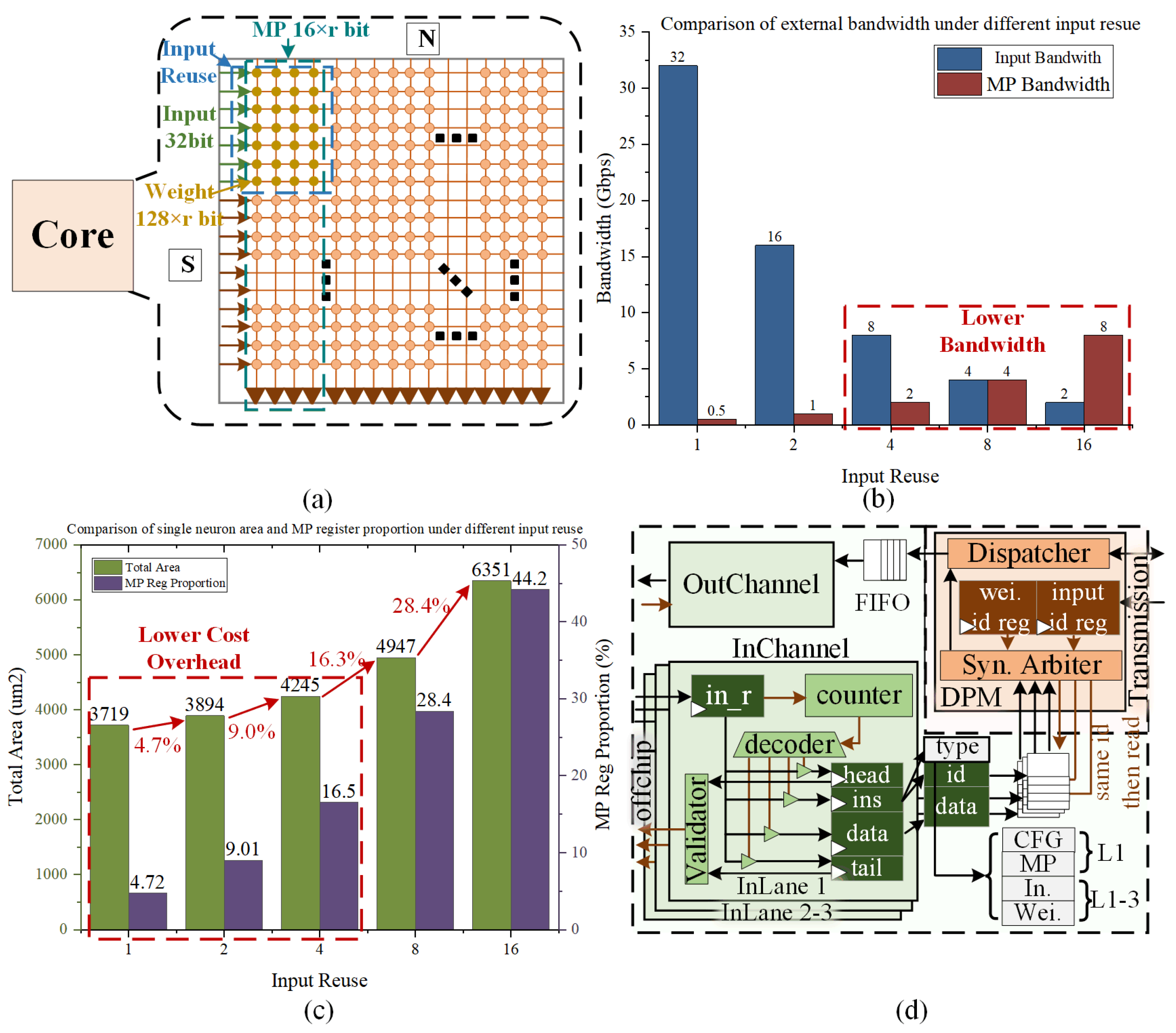
Although we utilized NVM to store weight data, significantly reducing the bandwidth demand of the computation core, the statistical results in Figure 5a also indicate that input bandwidth overhead cannot be ignored. Therefore, in our architecture, the data flow of the computation core is modified, as shown in Figure 6a, with a proposed input reuse method to alleviate external bandwidth pressure. For a set of incoming input data, it is not only used for the computation of a single neuron but is repeatedly reused for the computations of different neurons. This means that the core simultaneously calculates the results of multiple neurons.
After adopting the input reuse method, let the reuse factor be r. For the computation of a single core in Figure 6a, the input bandwidth overhead B W i n is reduced to
B W i n = S × N r
where S represents the number of synapses and N represents the number of neurons. Figure 6b shows the external bandwidth requirements under different values of r, where the input bandwidth is significantly reduced. However, since computations for different neurons are required, the membrane potential data must be cached r times within the core.
Considering the bandwidth pressure illustrated in Figure 6b and the area overhead depicted in Figure 6c resulting from reuse, a 4× reuse factor was chosen to achieve an optimal balance between bandwidth and area overhead.

2.3.3. Multi-Lane Interface

Although the measures have alleviated the bandwidth constraints, high-bandwidth communication between the off-chip memory system and the HDNIP core array remains necessary to satisfy the residual bandwidth requirements and facilitate future expansion, as depicted in Figure 6d. The multi-lane interface comprises three parallel input lanes and a single output channel. Each input lane has a validator and decoder to parse incoming data packets from off-chip, stripping protocol headers/tails, extracting the payload, instruction, and an ID. Based on bandwidth requirements and data type, the lanes are specialized. Configuration and MP data, possessing lower bandwidth needs partially due to the TDM scheme reducing MP update frequency, are exclusively handled by Lane 1. High-bandwidth data, specifically input spikes and synaptic weights, can be transmitted across all three lanes to maximize throughput. Extracted data and associated identifiers are temporarily stored in lane-specific buffers before being processed by the DPM.
A synchronization mechanism is crucial given that input spike and weight data related to the same computational step may arrive asynchronously across the three input lanes. This is implemented via an ID-ACK handshake protocol coordinated between the off-chip data source. The DPM contains internal ID registers holding the expected transaction ID. The Synchronization Arbiter compares the ID of the data waiting in the input lane buffers with the corresponding expected internal ID. Data are only dispatched for computation when the ID matches exactly, effectively stalling lanes with mismatched or subsequent IDs. This ensures that data packets belonging to the same transaction are consumed coherently across the parallel lanes before processing proceeds to the next transaction, maintaining data integrity. Since CFG and MP data are serialized on Lane 1, they bypass this multi-lane ID synchronization. On the output side, the TDM core design significantly reduces the peak output data rate, allowing a single out channel, buffered by a FIFO, to adequately handle the transmission of both generated spikes and updated membrane potentials off-chip.
Our proposed design leverages NVM for weight storage to reduce external bandwidth overhead by 80%, while the pipelined universal near-memory read design alleviates bandwidth bottlenecks. The 4-input reuse further reduced the primary input spike bandwidth to 25% of its original requirement, resulting in a 95% decrease in overall data volume needing off-chip transmission. The multi-lane interface design, featuring three parallel input lanes and supported by dedicated input buffers and a DPM for distribution, was devised to directly address the increasing bandwidth requirements associated with a growing number of active cores and neurons. The aggregate bandwidth can be linearly expanded by employing these parallel data channels. Furthermore, the ID-ACK mechanism acts as an essential flow control protocol, ensuring data integrity, consistency, and synchronization across these parallel lanes, which is especially critical during concurrent operations across many active cores and prevents data overrun.
These bandwidth optimization strategies operate synergistically, encompassing near-memory computing for weight access, input reuse, a scalable multi-lane interface, and ID-ACK flow control. It ensures that the core array can continuously and reliably access necessary weights and input data to support sustained computation, even as the number of active cores and neurons grows, thereby preventing bottlenecks and supporting scalable performance.

3. Experiments and Results

3.1. Deployment of the Emulation System

We expanded upon our previous experiments [41] and performed detailed functional verification for circuit emulation using the S2C OmniArk emulator, as shown in Figure 7a, composed of 12 Quartus Stratix FPGAs. A deployment of the typical configuration for the HDNIP was implemented on the emulator, as shown in Table 1. We utilized 16 NVM macro arrays, each with a size of 3072 bits × 2048, totaling 100 Mbits. In the actual deployment on the emulator, DDR is used to store NVM data, serving as an equivalent mapping. The actual synthesized resource overhead is also reflected in Table 1, with 131 k ALMs used and 100.66 Mbits of DDR utilized. The clock frequency ratio of computation, interface, and NVM is 2:8:1. With an NVM bit width of 3072, near-memory computing achieves good throughput without bottlenecks.
In our emulation and verification framework (Figure 7b), the off-chip functionalities are realized within a software-based Runtime Server. This server, implemented primarily in C/C++, interfaces with the Verilog hardware emulator via the DPI-C protocol using SCE-MI. High-level AI model mapping from PyTorch 2.3.1 and driver functions reside in Python 3.10, generating configuration and data tensors deserialized and passed to the C/C++ layer. Within the Runtime Server, the Multi-Lane Hub and Mem Pool module manages the dynamic data flow, effectively simulating the routing and memory interactions discussed previously. Data are formatted using pack/unpack functions and buffered via thread-safe queues before transmission to/from the emulator. Concurrently, the Mem editor component manages synaptic weights generated by the high-level driver to program the emulated NVM.
The emulation system automatically partitions the HDNIP across 12 FPGAs. Figure 7c–e illustrate how the FPGAs are allocated, placed, and routed within the emulator. For the 10 M-scale architecture, the NVM is mapped using DDR, resulting in only boards 10 and 11 being extensively utilized. In contrast, boards 0–9 are sparsely deployed, with more resources dedicated to routing overhead. The layout of each module is shown in Figure 7d, with 69% of the overhead attributed to the computation core array, represented in brown. Unlike chip layouts and single-FPGA layouts, the layout of multi-FPGA partitions is tightly concentrated near the FPGA pads, as shown in the purple areas in Figure 7d. As a result, the DTM and DPM are partitioned onto boards 10 and 11, while the core cluster arrays on boards 7 and 9 are also placed near the pads to facilitate communication with other boards. Figure 7e shows the routing congestion levels. This congestion is manageable since the actual bottleneck of the simulation system is caused by PCB communication between different boards and DDR delay.

3.2. Emulation Deployment of Neural Network Architectures

Furthermore, while the platform utilizes a simple neuron model, our validation on complex tasks demonstrates its high capability. As detailed in Table 2, various networks were successfully mapped and deployed on the HDNIP emulation system. This includes the successful deployment of a large-scale Spikingformer on the ImageNet dataset, which proves that network-level architectural complexity can effectively solve challenging problems, even with computationally simple neurons. We argue that massive scale is, in itself, a crucial capability. By providing a single-chip platform with 10 million neurons, HDNIP opens the door to a new class of complex, scale-dependent applications in both AI and computational neuroscience that were previously intractable on a single device.

3.2.1. N-MNIST

We deployed SNN on the HDNIP to recognize N-MNIST, with a structure consisting of three fully connected layers (2304 × 1024 × 512 × 10). The networks were fully mapped onto the platform, with each FCC handling one layer of data for 16 images, using 78 FCCs to recognize 416 data samples. Figure 8a shows the datasets’ batch recognition accuracy for 10 k images. LUT and weight states were obtained using layer-wise quantization and K-means clustering. The accuracy of our emulator-simulated network batches is shown by the blue squares in Figure 8a, achieving an average accuracy of 98.45%, which remains excellent compared to the full-precision software recognition accuracy of 98.54%.

3.2.2. CIFAR-10

Our work trained a Spikingformer [29] to infer the CIFAR-10 dataset. The Spiking Self-Attention (SSA) module was deployed on the emulator. The number of heads is 12, resulting in the linear layer scale for Query, Key, and Value being 384 × 384. We used a core size of 96 × 32 to deploy the linear layers, utilizing 72 FCCs, with 9 FCCs per layer. The computation for Q K T V was deployed on the remaining 8 FCCs, with a core size of 32 × 8192. The software result is 94.37%, as shown in Figure 9b—orange line. Table 2 shows that only 8 data samples were deployed on the HDNIP, and results for a random selection of 1000 data samples in blue squares indicate that the accuracy did not significantly drop, achieving an accuracy of 94.09%. In contrast to deployed quantized CNN models, Liu et al. [49] achieved an accuracy of 91.53% on a 5.1 M-parameter CNN employing 9-bit quantization on Loihi. At the same time, Tianjic [19,20] attained an accuracy of 93.52% with an int8-quantized VGG-8 model comprising 5.7 M parameters.

3.2.3. ImageNet

To validate the effectiveness of large-scale data, we employed the dataset from Spikingformer-8-768 to perform deployment validation on the ImageNet-1k dataset. In the emulator deployment, we unfolded the 196 eight-head outputs from the SSA for linear layer computation, with each linear layer consuming 768 × 768 operations. A set of unfolded linear layers utilized 49 cores, each with dimensions of 768 × 3072, and employed a 4-NF fusion strategy. Additionally, 80 FCCs were deployed to compute the SSA component within eight Transformer layers. The open-source Spikingformer-8-768 model achieved an accuracy of 75.68%, as depicted in Figure 8c. After executing the emulator simulation on a random sample of 1000 images, shown as blue squares in Figure 8c, the HDNIP achieved an accuracy of 74.2%, demonstrating its efficacy.

3.3. Results and Measurements

3.3.1. Chip Synthesies

The architecture proposed in this paper, excluding the NVM, was synthesized using the SMIC 40 nm process at 200 MHz, yielding the results shown in Figure 9a. The total synthesized area of the HDNIP is 9.88 mm 2 , with the cores accounting for 70.16%, which is close to the 69% layout proportion seen in the emulator’s layout in Figure 7d. Under the same clock frequency as specified in Table 1, near-memory computing operating with 8192 fully multiplexed cores exhibited a power consumption (excluding NVM) of 119.22 mW, with cores accounting for 67.92% of the total. The power consumption of the external interface diluted this proportion.
For the general compact-weight near-memory computing, a 100 Mbits ReRAM memory replaces SRAM. Table 3 shows that the ReRAM IP demonstrates a 1.9-times reduction in area and a 2.25-times reduction in power consumption compared to SRAM, closely aligning with the data reported in other studies [50,51]. Considering the area overhead of the NVM storage, as shown in Table 3, the HDNIP architecture achieves a 1.7-times reduction in area and a 1.2-times reduction in power compared to the SRAM-based version.

3.3.2. NMC and Off-Chip Computing Measurements

By incorporating the ReRAM IP, 1280 cores were utilized, thereby realizing an overall throughput of 13.64 GSOP/s with a total power consumption of 146.37 mW. Conversely, in the absence of ReRAM, with weights being supplied from off-chip, overall performance was constrained by a bandwidth bottleneck, yielding a throughput of 1.4 GSOP/s and a power consumption of 83.41 mW. The current evaluation used randomized networks and workloads rather than specific ones. A comprehensive configuration was adopted, with all 1280 cores active, a TDM factor of 8192, and complete consideration of power consumption.
As shown in Figure 9b, the results indicate that the throughput improvement achieved by using NVM near-memory computation is up to 9.7 times, primarily due to a 9.0-times increase in bandwidth. The throughput improvement exceeding 9.0 times is attributed to the reduction in external bandwidth loss, which improved the actual bandwidth utilization. The average maximum energy efficiency ratio is 10.73 pJ/SOP, which is 5.5 times higher than the energy efficiency ratio of off-chip computation. The throughput and energy efficiency improvements of near-memory computing benefit from alleviating external bandwidth bottlenecks. The bandwidth bottleneck is eliminated by adopting general-weight near-memory computing and input reuse designs.

3.3.3. Core Fusion Measurements

HDNIP’s flexible architecture, featuring variable-scale cores and core fusion, significantly enhances mapping efficiency compared to fixed-scale designs. For instance, when deploying a 384 × 384 linear layer (e.g., in Spikingformer for Cifar-10), a prior fixed-core approach suffered from very low utilization (14%) and 7.1-times higher latency. In contrast, HDNIP’s variable-scale cores achieve nearly 100% utilization. Furthermore, its core fusion mechanism can parallelize computation across 48-times more resources (e.g., using 4-way synapse and 12-way neuron fusion), theoretically reducing latency 48-fold while maintaining 100% utilization.
Cycle-accurate simulations demonstrate these benefits: the previous fixed-scale work [40] took 126.7 ms with a 0.223 GSOP/s throughput for one linear layer. HDNIP with variable-scale cores reduced runtime 14.2-fold and doubled throughput to 0.531 GSOP/s. Employing core fusion across 72 FCCs further slashed runtime to 0.2654 ms (a 477-fold improvement over the previous work) and boosted throughput to 13.3 GSOP/s. While this high parallelism revealed a minor input bottleneck due to the synapse TDM factor of 96 (which a larger TDM could alleviate), the results strongly affirm the substantial performance gains from HDNIP’s architectural flexibility.
To quantify the trade-off between density and latency inherent to our high TDM factor, we analyzed the neuron update rate under varying core configurations. The results highlight HDNIP’s designed versatility. When mapping smaller, agile networks (e.g., a 96 × 32 virtual array), a core achieves a high update rate of 3380 Hz, suitable for real-time applications, with latency further reducible via our core fusion mechanism. Conversely, when configured for maximum capacity with an 8192 × 8192 array, the rate becomes 0.16 Hz. This lower rate is tailored for high-throughput, non-real-time tasks such as large-scale scientific simulations, where emulating the network’s full complexity is prioritized over single-step latency. Thus, HDNIP’s adaptive architecture allows it to effectively serve a wide spectrum of applications, from latency-sensitive tasks to massive-scale computational research.

3.4. Comparison

3.4.1. Comparison with Conventional GPU

As mentioned in the introduction, traditional high-performance GPU architectures are inefficient when handling sparse, event-driven spiking neural networks. To quantify this disparity, we compared HDNIP with the top-tier NVIDIA RTX 4090 GPU while executing the Spikingformer (ImageNet) task, as mentioned in Table 4. The results clearly highlight the advantages of a specialized architecture; although the RTX 4090 achieves high performance at 28.12 TSOPS, its power consumption reaches 450 W, resulting in an energy efficiency of only 16.00 pJ/SOPS.
In contrast, HDNIP delivers an exceptional energy efficiency of 10.73 pJ/SOP while consuming just 146.37 mW, outperforming the RTX 4090 by approximately 1.5×. More importantly, HDNIP’s power consumption is over three orders of magnitude lower than that of the GPU. This significant advantage in energy efficiency and power consumption validates our core argument: despite GPUs’ high computational power, their substantial energy overhead makes them unsuitable for SWaP-constrained edge applications. For deploying large-scale SNNs in energy-limited scenarios, specialized high-density platforms like HDNIP represent a more feasible and efficient solution.

3.4.2. Comparison with Other Neuromorphic Works

The HDNIP achieved 10 million neurons and 80 G synapses using a synthesized area of 9.88 mm 2 without NVM’s area and 44.39 mm 2 with 100 Mbits ReRAM. We use the number of virtual neurons N n e u . that can be deployed per unit area as a measure of the architecture’s density, as shown below:
ρ n e u . = N n e u . A r e a
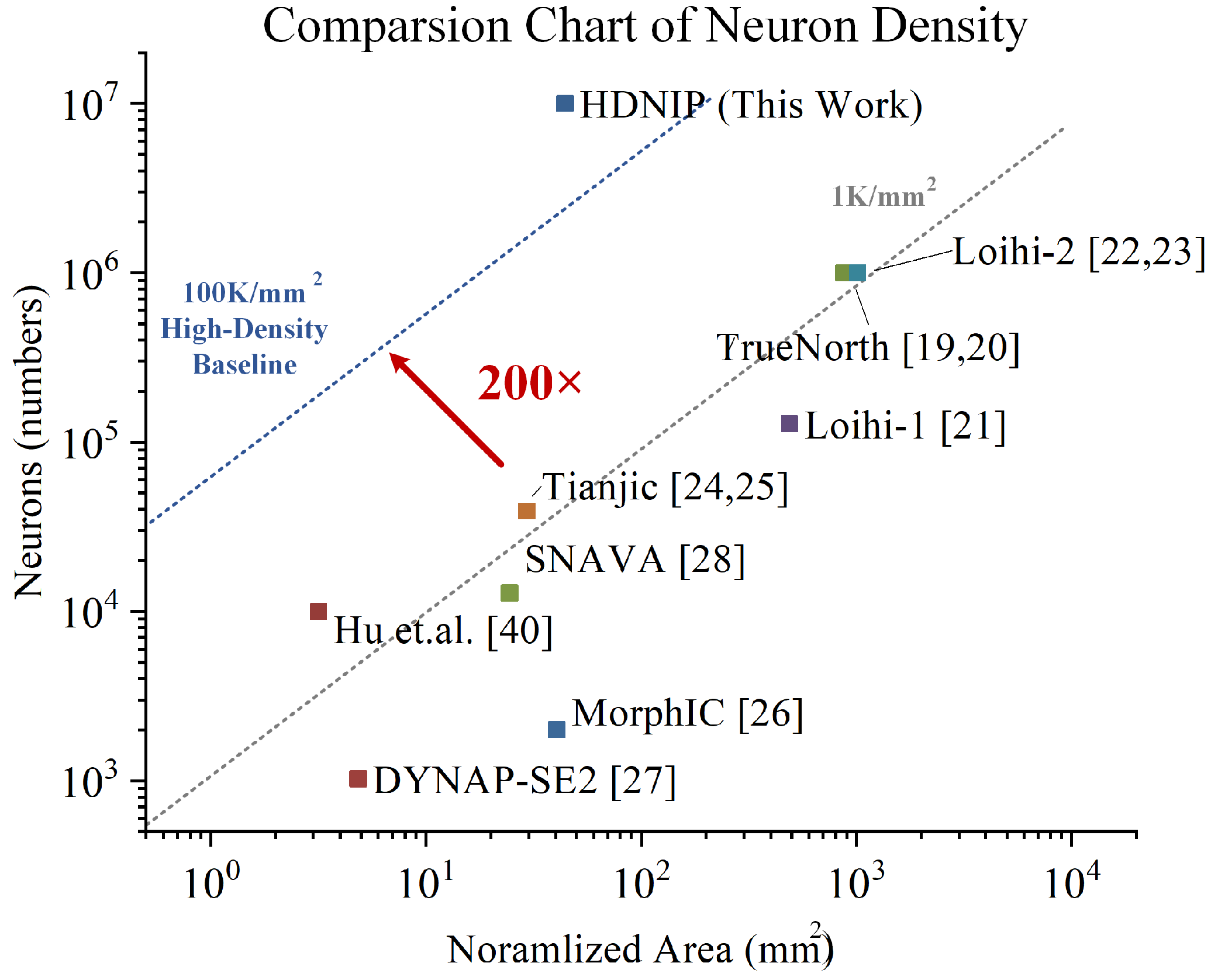
Table 5 indicates whether HDNIP incorporates NVM, and when normalized to the same process node, its neuron density outperforms other works by 2–3 orders of magnitude. As illustrated in Figure 10, the neuron density of other works normalized to a 40 nm process is approximately 1 K/ mm 2 . In contrast, this design’s HDNIP achieves a 225–1012 K/ mm 2 density, which is remarkably 71–320-times greater than the results of our previous work [40] and far ahead of other works. This approach involved not only architectural choices, such as removing low-density SRAM and employing a highly reusable core, but also a deliberate focus on inference by implementing a computationally efficient neuron model and omitting area-intensive features like on-chip learning. Additionally, the synthesized area, rather than the chip layout and routing area, makes the density improvement very significant. However, the density improvement remains highly substantial even when accounting for layout, routing, and more NVM overhead. HDNIP’s neuron density is already two-times higher than our proposed high-density baseline, offering promise for deploying brain-scale, human-brain-like simulations on a single device with SOTA technology.
Table 5 reports throughput measured at the maximum sustainable clock (or equivalent asynchronous scan rate) with all virtual neurons active. The proposed HDNIP integrates 1280 cores and operates at a 50 MHz, achieving 13.64 GSOP/s. In contrast, the design reported by Hu et al. [40] incorporates nine cores operating at 100 MHz, yielding 0.22 GSOP/s, while MorphIC [26] implements four cores operating at 55 MHz to achieve 0.11 GSOP/s. Moreover, TrueNorth [52] features 4096 asynchronous cores and, when normalized to an equivalent 65 MHz scan frequency, sustains 2.99 GSOP/s.
Table 5 reports two harmonized metrics: energy per synaptic operation (pJ/SOP) and normalized compute density (MSOPS/ mm 2 ) to facilitate a fair cross-chip assessment. In contrast to neuron density, which represents the network deployment capacity per unit area, computational density denotes the throughput per unit area. Our HDNIP achieves leading performance with 10.7 pJ/SOP and 307 MSOPS/ mm 2 , significantly outperforming our previous work [40] (33.26 pJ/SOP, 69 MSOPS/ mm 2 ) by offering an efficiency ratio of 3 times and computational density of 4.4 times. In terms of energy efficiency, the HDNIP architecture exhibits certain deficiencies relative to Tianjic’s work [24,25], yet outperforms other approaches; moreover, it achieves a 3.7× improvement in computational density over MorphIC [26]. Therefore, the HDNIP architecture achieves high neural density and, through architectural optimization, attains elevated performance; compared with other works, it exhibits a competitive energy efficiency ratio and superior computational density.

4. Conclusions and Discussion

In conclusion, this work presents a high-density neuromorphic inference platform that surmounts key hurdles in scaling neuromorphic hardware. The proposed architecture combines several novel strategies: elimination of on-chip SRAM, ReRAM-based NMC, input reuse, and adaptive TDM with core fusion, boosting neuron integration density, performance, and utilization efficiency beyond what prior designs have achieved. Through these techniques, HDNIP delivers a single-chip capacity of up to 10 million spiking neurons and 80 billion synapses, reaching 225 K/ mm 2 and demonstrating effective inferencing throughput on the 13 GSOP/s at 146 mW power. Regarding neuronal density, neuromorphic processors have improved by two orders of magnitude compared to the most advanced neuromorphic processors, effectively bridging the long-standing density gap between silicon neural engines and biological engines.
The HDNIP architecture demonstrates that a density-first design can achieve high performance by leveraging advanced memory technologies like ReRAM and carefully considered architecture-level adaptations. Its design is particularly well suited for large-scale spiking neural network inference in energy-constrained scenarios, where maximizing neuron numbers and energy efficiency is paramount. A key aspect of this density-first approach was the intentional focus on inference, utilizing a computationally efficient LIF neuron model while omitting area-intensive on-chip learning mechanisms like STDP. Crucially, this simplification at the neuron level does not limit the platform to simple problems; our successful deployment of complex models like the Spikingformer on the ImageNet dataset demonstrates that network-level architectural complexity can effectively address challenging, large-scale tasks. The platform’s adaptive TDM is engineered to effectively manage resource utilization and throughput for its target SNN workloads. While the inherent nature of time-multiplexing might require careful consideration for applications with exceptionally stringent, hard real-time constraints, this is a common trade-off for the significant density achieved. Furthermore, reliance on an off-chip interface is addressed through a scalable multi-lane design that allows for future external high-throughput interface (e.g., NVLink [53], SerDes [54]), expected to provide enough bandwidth to support even cortex-scale network models.
The design experience with HDNIP offers valuable insights for the field: the considerable potential of aggressive on-chip memory reduction, the importance of co-designing computation with advanced memory solutions, and the benefits of architectural flexibility. Building upon the high-density foundation established by HDNIP, our future work will focus on integrating on-chip learning capabilities, such as STDP, and more complex neuron dynamics, exploring novel circuit and architectural techniques to balance the trade-off between neuron density and functional complexity. Overall, HDNIP represents a notable step in neuromorphic VLSI, suggesting a viable direction for embedding many neurons on a single chip and inspiring future architectures to continue advancing towards bio-inspired neural computation.

Author Contributions

Conceptualization, Y.Z. and N.N.; methodology, Y.Z.; software, L.M., R.M.; validation, K.C., R.Z. and C.F.; formal analysis, S.W.; investigation, G.Q.; resources, Y.L.; writing—original draft preparation, Y.Z. and S.H.; writing—review and editing, Y.Z. and S.H. All authors have read and agreed to the published version of the manuscript.

Funding

This work was supported in part by STI 2030-Major Projects 2022ZD0209700 and in part by the Sichuan Provincial Science and Technology Programs (Grant No. 2024ZDZX0001 and Grant No. 2024ZYD0253).

Institutional Review Board Statement

Not applicable.

Informed Consent Statement

Not applicable.

Data Availability Statement

The original contributions presented in this study are included in the article. Further inquiries can be directed to the corresponding author.

Acknowledgments

The authors gratefully acknowledge the support provided by the University of Electronic Science and Technology of China (UESTC).

Conflicts of Interest

The authors declare no conflicts of interest. The funders had no role in the design of the study; in the collection, analyses, or interpretation of data; in the writing of the manuscript; or in the decision to publish the results.

References

  1. Mehonic, A.; Kenyon, A.J. Brain-inspired computing needs a master plan. Nature 2022, 604, 255–260. [Google Scholar] [CrossRef]
  2. Li, G.; Deng, L.; Tang, H.; Pan, G.; Tian, Y.; Roy, K.; Maass, W. Brain-Inspired Computing: A Systematic Survey and Future Trends. Proc. IEEE 2024, 112, 544–584. [Google Scholar] [CrossRef]
  3. Zhang, W.; Ma, S.; Ji, X.; Liu, X.; Cong, Y.; Shi, L. The development of general-purpose brain-inspired computing. Nat. Electron. 2024, 7, 954–965. [Google Scholar] [CrossRef]
  4. Shrestha, A.; Fang, H.; Mei, Z.; Rider, D.P.; Wu, Q.; Qiu, Q. A survey on neuromorphic computing: Models and hardware. IEEE Circuits Syst. Mag. 2022, 22, 6–35. [Google Scholar] [CrossRef]
  5. Furber, S. Large-scale neuromorphic computing systems. J. Neural Eng. 2016, 13, 051001. [Google Scholar] [CrossRef]
  6. Jouppi, N.P.; Young, C.; Patil, N.; Patterson, D.; Agrawal, G.; Bajwa, R.; Bates, S.; Bhatia, S.; Boden, N.; Borchers, A. In-datacenter performance analysis of a tensor processing unit. In Proceedings of the 2017 ACM/IEEE 44th Annual International Symposium on Computer Architecture (ISCA), Toronto, ON, Canada, 24–28 June 2017; pp. 1–12. [Google Scholar]
  7. Tirumala, A.; Wong, R. Nvidia blackwell platform: Advancing generative ai and accelerated computing. In Proceedings of the 2024 IEEE Hot Chips 36 Symposium (HCS), Stanford, CA, USA, 25–27 August 2024; pp. 1–33. [Google Scholar]
  8. Rathi, N.; Chakraborty, I.; Kosta, A.; Sengupta, A.; Ankit, A.; Panda, P.; Roy, K. Exploring neuromorphic computing based on spiking neural networks: Algorithms to hardware. ACM Comput. Surv. 2023, 55, 1–49. [Google Scholar] [CrossRef]
  9. Basu, A.; Deng, L.; Frenkel, C.; Zhang, X. Spiking Neural Network Integrated Circuits: A Review of Trends and Future Directions. In Proceedings of the 2022 IEEE Custom Integrated Circuits Conference (CICC), Newport Beach, CA, USA, 24–27 April 2022; pp. 1–8. [Google Scholar] [CrossRef]
  10. Kuang, Y.; Cui, X.; Wang, Z.; Zou, C.; Zhong, Y.; Liu, K.; Dai, Z.; Yu, D.; Wang, Y.; Huang, R. ESSA: Design of a Programmable Efficient Sparse Spiking Neural Network Accelerator. IEEE Trans. Very Large Scale Integr. (VLSI) Syst. 2022, 30, 1631–1641. [Google Scholar] [CrossRef]
  11. Tan, P.Y.; Wu, C.W. A 40-nm 1.89-pJ/SOP Scalable Convolutional Spiking Neural Network Learning Core With On-Chip Spatiotemporal Back-Propagation. IEEE Trans. Very Large Scale Integr. (VLSI) Syst. 2023, 31, 1994–2007. [Google Scholar] [CrossRef]
  12. Xie, C.; Shao, Z.; Chen, Z.; Du, Y.; Du, L. An Energy-Efficient Spiking Neural Network Accelerator Based on Spatio-Temporal Redundancy Reduction. IEEE Trans. Very Large Scale Integr. (VLSI) Syst. 2024, 32, 782–786. [Google Scholar] [CrossRef]
  13. Cadwell, C.R.; Bhaduri, A.; Mostajo-Radji, M.A.; Keefe, M.G.; Nowakowski, T.J. Development and arealization of the cerebral cortex. Neuron 2019, 103, 980–1004. [Google Scholar] [CrossRef]
  14. Ballard, D.H. Cortical connections and parallel processing: Structure and function. Behav. Brain Sci. 1986, 9, 67–90. [Google Scholar] [CrossRef]
  15. Mosier, K.; Bereznaya, I. Parallel cortical networks for volitional control of swallowing in humans. Exp. Brain Res. 2001, 140, 280–289. [Google Scholar] [CrossRef] [PubMed]
  16. Herculano-Houzel, S. The human brain in numbers: A linearly scaled-up primate brain. Front. Hum. Neurosci. 2009, 3, 31. [Google Scholar] [CrossRef] [PubMed]
  17. Azevedo, F.A.; Carvalho, L.R.; Grinberg, L.T.; Farfel, J.M.; Ferretti, R.E.; Leite, R.E.; Filho, W.J.; Lent, R.; Herculano-Houzel, S. Equal numbers of neuronal and nonneuronal cells make the human brain an isometrically scaled-up primate brain. J. Comp. Neurol. 2009, 513, 532–541. [Google Scholar] [CrossRef]
  18. Pakkenberg, B.; Gundersen, H.J.G. Neocortical neuron number in humans: Effect of sex and age. J. Comp. Neurol. 1997, 384, 312–320. [Google Scholar] [CrossRef]
  19. Merolla, P.A.; Arthur, J.V.; Alvarez-Icaza, R.; Cassidy, A.S.; Sawada, J.; Akopyan, F.; Jackson, B.L.; Imam, N.; Guo, C.; Nakamura, Y. A million spiking-neuron integrated circuit with a scalable communication network and interface. Science 2014, 345, 668–673. [Google Scholar] [CrossRef]
  20. Akopyan, F.; Sawada, J.; Cassidy, A.; Alvarez-Icaza, R.; Arthur, J.; Merolla, P.; Imam, N.; Nakamura, Y.; Datta, P.; Nam, G.J. Truenorth: Design and tool flow of a 65 mw 1 million neuron programmable neurosynaptic chip. IEEE Trans. Comput.-Aided Des. Integr. Circuits Syst. 2015, 34, 1537–1557. [Google Scholar] [CrossRef]
  21. Davies, M.; Srinivasa, N.; Lin, T.H.; Chinya, G.; Cao, Y.; Choday, S.H.; Dimou, G.; Joshi, P.; Imam, N.; Jain, S. Loihi: A neuromorphic manycore processor with on-chip learning. IEEE Micro 2018, 38, 82–99. [Google Scholar] [CrossRef]
  22. Orchard, G.; Frady, E.P.; Rubin, D.B.D.; Sanborn, S.; Shrestha, S.B.; Sommer, F.T.; Davies, M. Efficient neuromorphic signal processing with loihi 2. In Proceedings of the 2021 IEEE Workshop on Signal Processing Systems (SiPS), Coimbra, Portugal, 20–22 October 2021; pp. 254–259. [Google Scholar]
  23. Davies, M. Taking neuromorphic computing to the next level with Loihi2. Intel Labs’ Loihi 2021, 2, 1–7. [Google Scholar]
  24. Pei, J.; Deng, L.; Song, S.; Zhao, M.; Zhang, Y.; Wu, S.; Wang, G.; Zou, Z.; Wu, Z.; He, W. Towards artificial general intelligence with hybrid Tianjic chip architecture. Nature 2019, 572, 106–111. [Google Scholar] [CrossRef]
  25. Deng, L.; Wang, G.; Li, G.; Li, S.; Liang, L.; Zhu, M.; Wu, Y.; Yang, Z.; Zou, Z.; Pei, J. Tianjic: A unified and scalable chip bridging spike-based and continuous neural computation. IEEE J. -Solid-State Circuits 2020, 55, 2228–2246. [Google Scholar] [CrossRef]
  26. Frenkel, C.; Legat, J.D.; Bol, D. MorphIC: A 65-nm 738k-Synapse/mm2 Quad-Core Binary-Weight Digital Neuromorphic Processor With Stochastic Spike-Driven Online Learning. IEEE Trans. Biomed. Circuits Syst. 2019, 13, 999–1010. [Google Scholar] [CrossRef]
  27. Richter, O.; Wu, C.; Whatley, A.M.; Köstinger, G.; Nielsen, C.; Qiao, N.; Indiveri, G. DYNAP-SE2: A scalable multi-core dynamic neuromorphic asynchronous spiking neural network processor. Neuromorphic Comput. Eng. 2024, 4, 014003. [Google Scholar] [CrossRef]
  28. Sripad, A.; Sanchez, G.; Zapata, M.; Pirrone, V.; Dorta, T.; Cambria, S.; Marti, A.; Krishnamourthy, K.; Madrenas, J. SNAVA—A real-time multi-FPGA multi-model spiking neural network simulation architecture. Neural Netw. 2018, 97, 28–45. [Google Scholar] [CrossRef] [PubMed]
  29. Zhou, C.; Yu, L.; Zhou, Z.; Ma, Z.; Zhang, H.; Zhou, H.; Tian, Y. Spikingformer: Spike-driven residual learning for transformer-based spiking neural network. arXiv 2023, arXiv:2304.11954. [Google Scholar]
  30. Zhu, R.J.; Zhao, Q.; Li, G.; Eshraghian, J.K. Spikegpt: Generative pre-trained language model with spiking neural networks. arXiv 2023, arXiv:2302.13939. [Google Scholar]
  31. Harbour, S.; Sears, B.; Schlager, S.; Kinnison, M.; Sublette, J.; Henderson, A. Real-time vision-based control of swap-constrained flight system with intel loihi 2. In Proceedings of the 2023 IEEE/AIAA 42nd Digital Avionics Systems Conference (DASC), Barcelona, Spain, 1–5 October 2023; pp. 1–6. [Google Scholar]
  32. Perryman, N.; Wilson, C.; George, A. Evaluation of xilinx versal architecture for next-gen edge computing in space. In Proceedings of the 2023 IEEE Aerospace Conference, Big Sky, MT, USA, 4–11 March 2023; pp. 1–11. [Google Scholar]
  33. Shamwell, E.J.; Nothwang, W.D.; Perlis, D. A deep neural network approach to fusing vision and heteroscedastic motion estimates for low-SWaP robotic applications. In Proceedings of the 2017 IEEE International Conference on Multisensor Fusion and Integration for Intelligent Systems (MFI), Daegu, Republic of Korea, 16–18 November 2017; pp. 56–63. [Google Scholar]
  34. Neuman, S.M.; Plancher, B.; Duisterhof, B.P.; Krishnan, S.; Banbury, C.; Mazumder, M.; Prakash, S.; Jabbour, J.; Faust, A.; de Croon, G.C.; et al. Tiny robot learning: Challenges and directions for machine learning in resource-constrained robots. In Proceedings of the 2022 IEEE 4th International Conference on Artificial Intelligence Circuits and Systems (AICAS), Incheon, Republic of Korea, 13–15 June 2022; pp. 296–299. [Google Scholar]
  35. Kudithipudi, D.; Schuman, C.; Vineyard, C.M.; Pandit, T.; Merkel, C.; Kubendran, R.; Aimone, J.B.; Orchard, G.; Mayr, C.; Benosman, R. Neuromorphic computing at scale. Nature 2025, 637, 801–812. [Google Scholar] [CrossRef]
  36. Chicca, E.; Stefanini, F.; Bartolozzi, C.; Indiveri, G. Neuromorphic Electronic Circuits for Building Autonomous Cognitive Systems. Proc. IEEE 2014, 102, 1367–1388. [Google Scholar] [CrossRef]
  37. Wu, S.Y.; Lin, C.; Chiang, M.; Liaw, J.; Cheng, J.; Yang, S.; Tsai, C.; Chen, P.; Miyashita, T.; Chang, C.; et al. A 7nm CMOS platform technology featuring 4 th generation FinFET transistors with a 0.027 μm 2 high density 6-T SRAM cell for mobile SoC applications. In Proceedings of the 2016 IEEE International Electron Devices Meeting (IEDM), San Francisco, CA, USA, 3–7 December 2016; pp. 2–6. [Google Scholar]
  38. Yeap, G.; Lin, S.; Chen, Y.; Shang, H.; Wang, P.; Lin, H.; Peng, Y.; Sheu, J.; Wang, M.; Chen, X.; et al. 5nm cmos production technology platform featuring full-fledged euv, and high mobility channel finfets with densest 0.021 μm 2 sram cells for mobile soc and high performance computing applications. In Proceedings of the 2019 IEEE International Electron Devices Meeting (IEDM), San Francisco, CA, USA, 7–11 December 2019; pp. 36–37. [Google Scholar]
  39. Wu, S.Y.; Chang, C.H.; Chiang, M.; Lin, C.; Liaw, J.; Cheng, J.; Yeh, J.; Chen, H.; Chang, S.; Lai, K.; et al. A 3nm CMOS FinFlex™ platform technology with enhanced power efficiency and performance for mobile SoC and high performance computing applications. In Proceedings of the 2022 International Electron Devices Meeting (IEDM), San Francisco, CA, USA, 3–7 December 2022; pp. 27.5.1–27.5.4. [Google Scholar]
  40. Hu, S.; Qiao, G.; Liu, X.; Liu, Y.; Zhang, C.; Zuo, Y.; Zhou, P.; Liu, Y.; Ning, N.; Yu, Q. A Co-Designed Neuromorphic Chip With Compact (17.9 KF 2) and Weak Neuron Number-Dependent Neuron/Synapse Modules. IEEE Trans. Biomed. Circuits Syst. 2022, 16, 1250–1260. [Google Scholar] [CrossRef]
  41. Zuo, Y.; Ning, N.; Cao, K.; Zhang, R.; Wang, S.; Meng, L.; Qiao, G.; Liu, Y.; Hu, S. Design of a Highly Flexible Hybrid Neural Network Inference Platform with 10 Million Neurons. In Proceedings of the 2024 IEEE Biomedical Circuits and Systems Conference (BioCAS), Xi’an, China, 24–26 October 2024; pp. 1–5. [Google Scholar]
  42. He, K.; Zhang, X.; Ren, S.; Sun, J. Deep residual learning for image recognition. In Proceedings of the IEEE Conference on Computer Vision and Pattern Recognition, Las Vegas, NV, USA, 27–30 June 2016; pp. 770–778. [Google Scholar]
  43. Tang, Y.; Nyengaard, J.R.; De Groot, D.M.G.; Gundersen, H.J.G. Total regional and global number of synapses in the human brain neocortex. Synapse 2001, 41, 258–273. [Google Scholar] [CrossRef]
  44. Wang, Z.; Song, Y.; Zhang, G.; Luo, Q.; Xu, K.; Gao, D.; Yu, B.; Loke, D.; Zhong, S.; Zhang, Y. Advances of embedded resistive random access memory in industrial manufacturing and its potential applications. Int. J. Extrem. Manuf. 2024, 6, 032006. [Google Scholar] [CrossRef]
  45. Chen, A. A review of emerging non-volatile memory (NVM) technologies and applications. Solid-State Electron. 2016, 125, 25–38. [Google Scholar] [CrossRef]
  46. Kargar, S.; Nawab, F. Challenges and future directions for energy, latency, and lifetime improvements in NVMs. Distrib. Parallel Databases 2023, 41, 163–189. [Google Scholar] [CrossRef]
  47. Strenz, R. Review and outlook on embedded NVM technologies–from evolution to revolution. In Proceedings of the 2020 IEEE International Memory Workshop (IMW), Dresden, Germany, 17–20 May 2020; pp. 1–4. [Google Scholar]
  48. Kim, S.; Yoo, H.J. An Overview of Computing-in-Memory Circuits with DRAM and NVM. IEEE Trans. Circuits Syst. II Express Briefs 2023, 71, 1626–1631. [Google Scholar] [CrossRef]
  49. Liu, S.; Yi, Y. Unleashing Energy-Efficiency: Neural Architecture Search without Training for Spiking Neural Networks on Loihi Chip. In Proceedings of the 2024 25th International Symposium on Quality Electronic Design (ISQED), San Francisco, CA, USA, 3–5 April 2024; pp. 1–7. [Google Scholar]
  50. Zhao, L.; Chen, Z.; Manea, D.; Li, S.; Li, J.; Zhu, Y.; Sui, Z.; Lu, Z. Highly reliable 40nm embedded dual-interface-switching RRAM technology for display driver IC applications. In Proceedings of the 2022 IEEE Symposium on VLSI Technology and Circuits (VLSI Technology and Circuits), Honolulu, HI, USA, 12–17 June 2022; pp. 316–317. [Google Scholar]
  51. Prabhu, K.; Gural, A.; Khan, Z.F.; Radway, R.M.; Giordano, M.; Koul, K.; Doshi, R.; Kustin, J.W.; Liu, T.; Lopes, G.B. CHIMERA: A 0.92-TOPS, 2.2-TOPS/W edge AI accelerator with 2-MByte on-chip foundry resistive RAM for efficient training and inference. IEEE J. Solid-State Circuits 2022, 57, 1013–1026. [Google Scholar] [CrossRef]
  52. Cassidy, A.S.; Alvarez-Icaza, R.; Akopyan, F.; Sawada, J.; Arthur, J.V.; Merolla, P.A.; Datta, P.; Tallada, M.G.; Taba, B.; Andreopoulos, A.; et al. Real-time scalable cortical computing at 46 giga-synaptic OPS/watt with ~100× speedup in time-to-solution and ~100,000× reduction in energy-to-solution. In Proceedings of the SC’14: International Conference for High Performance Computing, Networking, Storage and Analysis, New Orleans, LA, USA, 16–21 November 2014; pp. 27–38. [Google Scholar]
  53. Wei, Y.; Huang, Y.C.; Tang, H.; Sankaran, N.; Chadha, I.; Dai, D.; Oluwole, O.; Balan, V.; Lee, E. 9.3 NVLink-C2C: A coherent off package chip-to-chip interconnect with 40Gbps/pin single-ended signaling. In Proceedings of the 2023 IEEE International Solid-State Circuits Conference (ISSCC), San Francisco, CA, USA, 19–23 February 2023; pp. 160–162. [Google Scholar]
  54. Segal, Y.; Laufer, A.; Khairi, A.; Krupnik, Y.; Cusmai, M.; Levin, I.; Gordon, A.; Sabag, Y.; Rahinski, V.; Ori, G.; et al. A 1.41 pJ/b 224Gb/s PAM-4 SerDes receiver with 31 dB loss compensation. In Proceedings of the 2022 IEEE International Solid-State Circuits Conference (ISSCC), Francisco, CA, USA, 20–26 February 2022; Volume 65, pp. 114–116. [Google Scholar]
Figure 1. HDNIP’s architecture diagram, adapted from [41], reprinted with permission from IEEE Proceedings. ©2024 IEEE.
Electronics 14 03412 g001
Figure 2. Computation core architecture diagram, including module circuit details. (a) The flexible core clusters, adapted from [41], reprinted with permission from IEEE Proceedings. ©2024 IEEE. (b) The compact core’s circuit design, adapted from [41], reprinted with permission from IEEE Proceedings. ©2024 IEEE. (c) The shared core fusion module schematic.
Electronics 14 03412 g002
Figure 3. The neuron–synapse scale diagram of ResNet-18 [42] and Transformer [29], where the synapses in the convolution part represent effective synapses, calculated as the product of convolution kernels and input channels.
Electronics 14 03412 g003
Figure 4. (a) Variable-scale core diagram supporting 32–8192, adapted from [41], reprinted with permission from IEEE Proceedings. ©2024 IEEE. (b) Core cluster supports arbitrary numbers of neuron fusion (NF). (c) Core cluster supports 2, 4, 8, and 16 synapse fusion (SF), represented by green, blue, red, and black, respectively.
Electronics 14 03412 g004
Figure 5. (a) Comparison of bandwidth overhead for weights, inputs, and membrane potentials required by each neuron in the designed core. (b) Comparison of different types of NVMs and SRAM [44,45,46]. (c) General circuit design for the NVM clock domain, where orange represents the control path, and black represents the data path.
Electronics 14 03412 g005
Figure 6. (a) Diagram of input reuse in the core. (b) Comparison of external bandwidth requirements for the computation core array under different input reuse scenarios at 50 MHz. (c) Core gate-level netlist area and membrane potential register area proportion under different reuse scenarios in a 40 nm process. (d) Circuit diagram of the multi-lane input protocol in the architecture, where orange arrows represent control paths and black arrows represent data paths.
Electronics 14 03412 g006
Figure 7. (a) Physical diagram of the deployed emulation system, including the emulator and Runtime Server. (b) Architecture diagram of the deployed system’s software and hardware components, connecting heterogeneous software and hardware data through deserialization and SCE-MI Protocol. (c) Partition ratio diagram of FPGA 0–11 on the emulator, where only 7, 9, 10, and 11 are utilized. (d) Module placement distribution diagram on the main FPGA board, where dark blue represents the effective resources deployed for the DUT and DTM and WTM are abbreviations for the Data Transmission Module and Weight Transmission Module, respectively. (e) Routing congestion level on the main FPGA board, with redder areas indicating higher congestion levels.
Electronics 14 03412 g007
Figure 8. Illustration of inference accuracy for HDNIP across three different datasets with varying random batches. The blue squares represent the final accuracy of individual batch data, while the average accuracy of hardware implementation (blue dashed line) shows only minor differences compared to the full-precision software baseline (orange). (a) N-MNIST’s accuracy; (b) Cifar-10’s accuracy; (c) ImageNet-1k’s accuracy.
Electronics 14 03412 g008
Figure 9. (a) A statistical chart of the synthesized area and power consumption proportions, with the inner circle representing the area distribution and the outer circle representing the power consumption distribution. (b) Throughput and bandwidth comparison between off-chip storage computation and near-memory computation. (c) Overhead comparison of different core cluster deployment methods, adapted from [41], reprinted with permission from IEEE Proceedings. ©2024 IEEE. (d) Comparison diagram of the runtime and throughput consumption between Hu et al. (our previous work) and the HDNIP (variable-scale and CF-scale) when executing eight SSA linear layers.
Electronics 14 03412 g009
Figure 10. A comparison chart of normalized area (under 40 nm process) versus neuron number across different works.
Electronics 14 03412 g010
Table 1. Configuration parameters and detailed FPGA overhead statistics of the HDNIP on the emulator.
Config. NameConfig. Param.Emu. ResourcesUtilization
Computation Clock50 MHzALM1,317,449
Interface Clock200 MHzLUT2,634,898
NVM Clock25 MHzFF785,843
NVM Bit Width3072 bitBRAM1,607,168
NVM Depth2048LUTRAM434
NVM Block16DDR100,663,296
Table 2. Deployment information of four model architectures for different types of tasks.
DatasetsArchitectureDeployed LayersBatch SizeFCC UtilizedNMC Throughput
N-MNIST3FC3FC4167813.29 GSOP/s
Cifar-103Tokenizer +2Transformer1Transformer88013.30 GSOP/s
ImageNet5Tokenizer +8Transformer8Transformer18013.59 GSOP/s
Table 3. A comparison of the area and power consumption of 100 Mbits SRAM and ReRAM, both individually and within the context of HDNIP.
Memory TypeMem. Area ( mm 2 )HDNIP Area ( mm 2 )Mem. Power (mW)HDNIP Power (mW)
SRAM4.1375.9561.16180.38
ReRAM2.1744.3927.15146.37
Table 4. Comparison of results between our work and GPU in the Spikingformer.
PlatformThis Work (HDNIP)RTX4090 (GPU)
Technology (nm)404
Power (mW)146.37450,000
Throughput (GSOP/s)13.6428,121
Energy Efficiency (pJ/SOP)10.7316.00
Table 5. Results of the architecture in this paper and comparison with similar works.
PlatformThis WorkHu et al. [40]True-North [19,20]Loihi-1 [21]Loihi-2 [22,23]Tianjic [24,25]Morph-IC [26]DYN-AP-SE2 [27]SNA-VA [28]
Technology (nm)405528147286518028
Clock (MHz)25–200 a100AsyncAsyncAsync30055/210Async125
Neuron Number10 M10 k1 M128 k1 M39 k2 k1 k12.8 k
Synapse Number80 G10 M256 M128 M114.4 M9.75 M2.06 M65 k20 k
Area ( mm 2 )44.396430603114.443.59812
Normalized neuron density (K/ mm 2 ) b225.283.151.140.260.991.321.50.210.52
Virtual Neurons Per Core819210242561024819225651211024
Core Number12809409612812815644100
Power (mW)146.3714.942–323--95019.9-625
Avg. Throughput (GSOP/s)13.640.222.99---0.11--
Energy Efficiency (pJ/SOP)10.7333.2621.7323.6-1.5451150-
Normalized Compute Density (MSOPS / mm 2 ) c3076934---83--
a The interface clock operates at 200 MHz, the computation clock at 50 MHz, and the NVM clock at 25 MHz, the same as Table 1. b The area is normalized to 40 nm, A r e a Normalized = A r e a × Tech . 40 2 . c The computational density: T h r o u g h p p u t A r e a N o r m a l i z e d .
Disclaimer/Publisher’s Note: The statements, opinions and data contained in all publications are solely those of the individual author(s) and contributor(s) and not of MDPI and/or the editor(s). MDPI and/or the editor(s) disclaim responsibility for any injury to people or property resulting from any ideas, methods, instructions or products referred to in the content.