Article

Injection-Locked Frequency Multipliers with Single Inductor Component

Department of Electronic Engineering, National Taiwan University of Science and Technology, Taipei 106335, Taiwan
*
Author to whom correspondence should be addressed.
Electronics 2025, 14(17), 3360; https://doi.org/10.3390/electronics14173360
Submission received: 10 July 2025 / Revised: 20 August 2025 / Accepted: 21 August 2025 / Published: 24 August 2025
(This article belongs to the Special Issue Advances in Frontend Electronics for Millimeter-Wave Systems)

Abstract

This paper proposes a compact inductor design for LC-tank injection-locked frequency multipliers (ILFMs) fabricated using a 0.18 μm CMOS process. The ILFMs use an 8-shaped inductor with two lobes, suppressing the magnetic field generation. Its contents cover one ×2, one ×3, and one ×6 ILFM. The first ×2 ILFM circuit uses the orthogonal transformer consisting of an 8-shaped inductor and a non-twisted inductor. The total area is 1.137 × 0.797 mm2. The input locking range is from the incident frequency of 1.6 to 3.0 GHz to provide a signal source from 3.2 GHz to 6 GHz. The second ×3 ILFM uses the orthogonal transformer and occupies an area of 1.29 × 0.76 mm2. The output locking range is from 9 GHz to 19.8 GHz. This third ×6 ILFM uses a trifilar consisting of two 8-shaped inductors in perpendicular layout and a non-twisted inductor. The ×6 ILFMs show interference noise suppression via a core two-turn 8-shaped inductor and save die area. The die area is 0.843 × 0.981 mm2. At VDD = 1.3 V and an input power of 0 dBm, the output locking range is from 5.16 GHz to 5.388 GHz. In all the investigated ILFMs, no varactors are added to the LC resonator for a wide-band locking range design. The phase noises of the input signal and the output signal of the ILFM are in agreement with the theoretical value.

1. Introduction

Injection-locked frequency multipliers (ILFMs) are popular circuits used with phase-locked loops (PLLs) [1] to extend the operation frequency. Fundamentally, they cover ×2 ILFMs [2,3,4], ×3 ILFMs [5,6,7] and other high-modulus ILFMs. A 5.7 GHz single-stage LC-tank injection-locked frequency sixtupler (ILFS) [8] has been presented and it uses several octagonal inductors. Two recent millimeter (mm)-wave ILFSs [9] with the schematic as shown in Figure 1a uses five O-shaped inductors or 8-shaped inductors, where the latter is used for magnetic coupling noise suppression. A mm-wave ×6 ILFM as shown in Figure 1b uses a frequency doubler in series with a frequency tripler. The use of multi-inductors increases the die area of the ILFM core and the harmonic coupling between the ILFM-core inductors; it also increases the distance between circuits because of magnetic field coupling.
This paper designs three LC-tank ILFMs fabricated using the CMOS process and the circuit uses only one compact inductive device for die area saving. In the first designed ×2 ILFM, two inductors are configured as a low-coupling orthogonal transformer consisting of an 8-shaped inductor and a non-twisted inductor. The orthogonal transformer [10] uses one 8-shaped inductor and one non-twisted inductor sharing the same hollow area and with a low-coupling coefficient. Because of the low-K coefficient, the two inductors are regarded as two isolated inductors, so the occupied area of the transformer is small. In addition, the 8-shaped inductor [11] reduces the magnetic field radiation by the opposed magnetic field directions due to the two inductor lobes. The second designed ×3 ILFM also uses a low-coupling orthogonal transformer. The previous ×3 ILFM shows a small locking range [12] because it uses varactors to extend the tuning range, but the varactors reduce the locking range, and it uses one buffer filter to reduce harmonics. The present ×3 ILFM without varactors enhances the locking range and uses two buffer filters to reduce the harmonics. The two-coil inductor design can be extended to a three-coil inductor design for ILFMs to save die area. The third designed ×6 ILFM uses a three-coil low-coupling orthogonal trifilar. Experiment verifies the possibility of an orthogonal trifilar.

2. Multiply-by-2 ILFM

A conventional ×2 ILF can be designed with three spiral inductors. The section designs a compact ×2 ILFM with one inductive component.

2.1. ×2 Circuit Design with Single Inductive Component

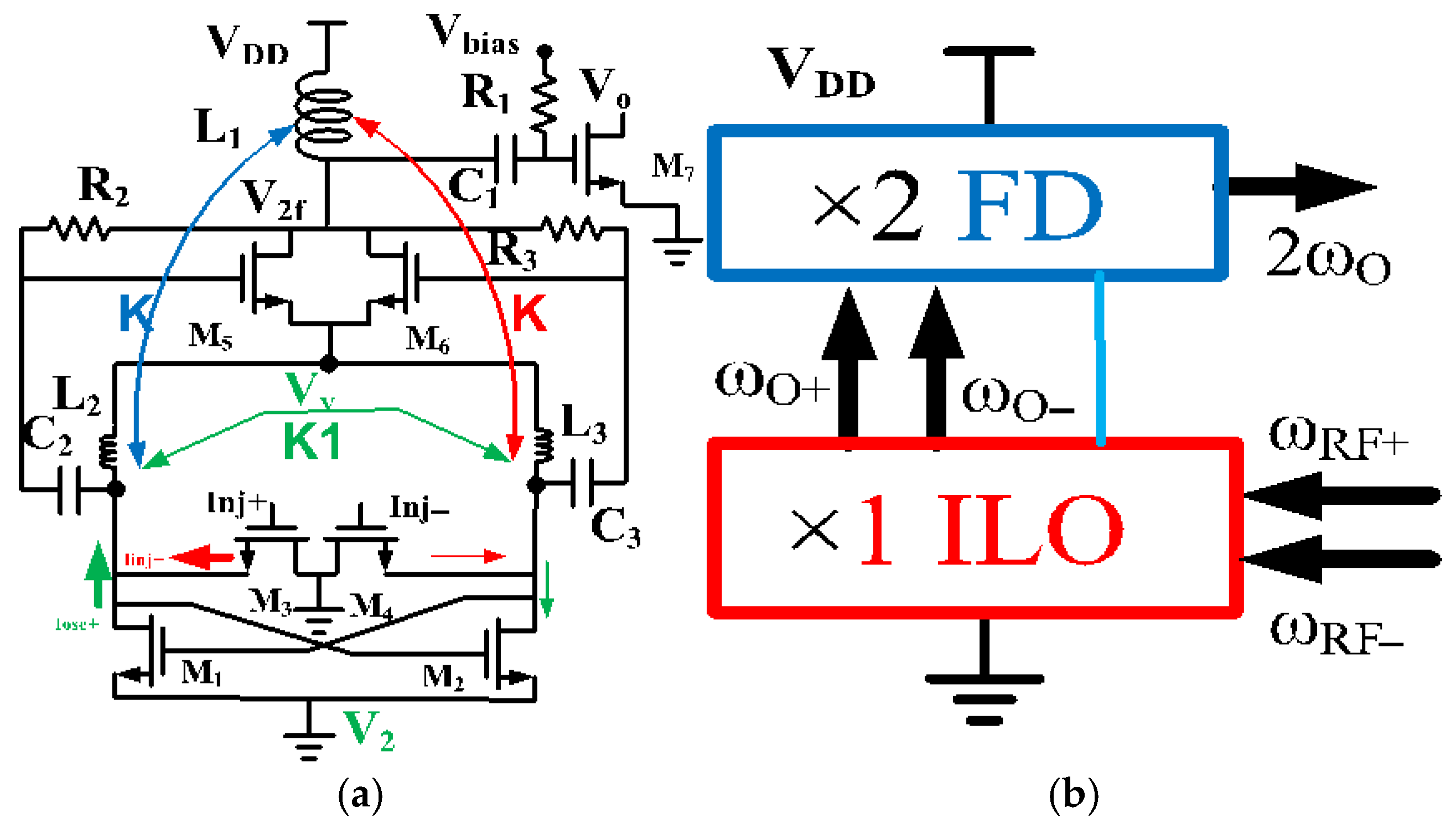
The schematic of the first ×2 ILFM circuit is shown in Figure 2a. Figure 2b shows the circuit block diagram with a differential input/output injection-locked oscillator (ILO) stacked below a single-ended output ×2 FD. The cross-coupled nMOS transistors M1 and M2 and two-turn center-tapped 8-shaped inductors made of L2, L3, and parasitic capacitors form a VCO used as a first-harmonic ILO with two injection nFETs M3 and M4. The common-source Vv of M5 and M6 is a virtual ground for the fundamental signal. A differential injection signal at the frequency finj is applied to the gates M3 and M4. NFETs M5 and M6, and inductor L1 form a balanced frequency doubler. The frequency doubler is based on the MOSFET used as a nonlinear amplifier, which generates the 2nd harmonic essential to the balanced frequency doubler. Transistor M7 is the output buffer for the extraction of the 2 finj signal, and the locking range of the 1st harmonic ILO determines the locking range of the ILFD. Components C1~C3 are DC-blocking capacitors. Components R1~R3 are for DC biasing. Vbias is the gate bias voltage. The nMOS VCO is used as a 1st harmonic ILO with the output oscillation frequency locked to the signal at finj, in case the frequency finj falls in the locking range of the 1st harmonic ILO. No buffer is used for the ILO; this reduces the parasitic capacitance and increases the locking range.
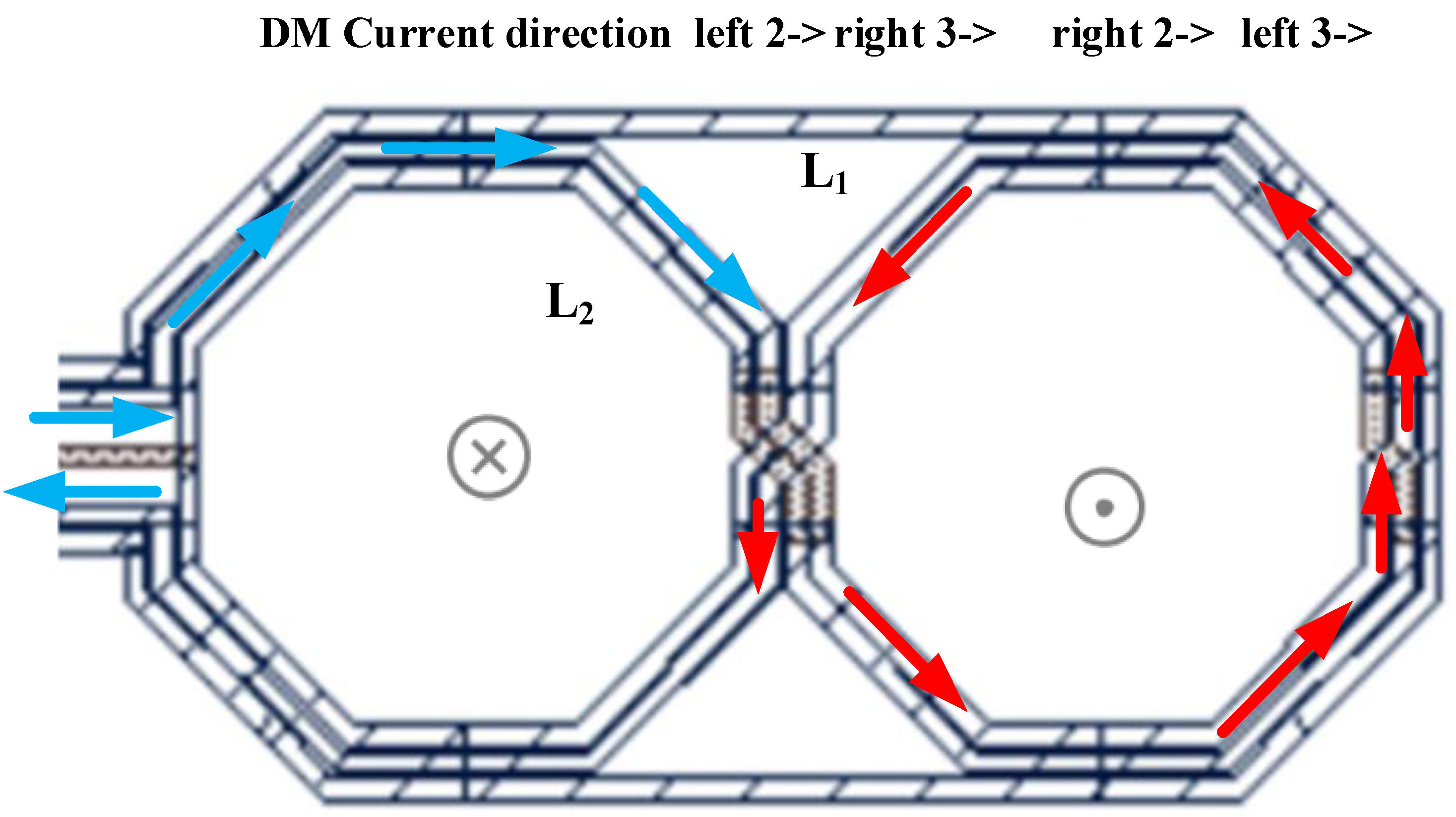
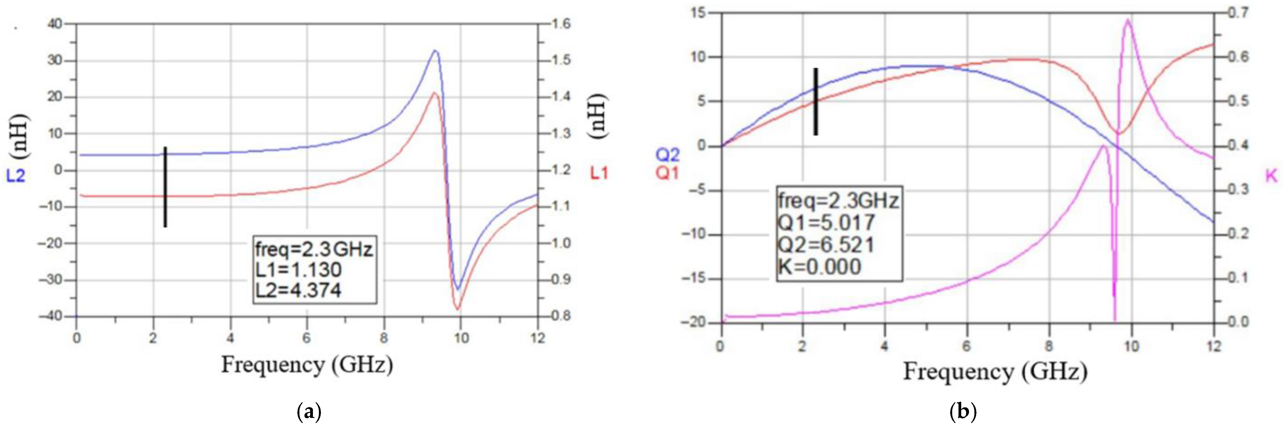
Figure 3 shows the layout of the orthogonal transformer consisting of one two-turn 8-shaped inductor laid inside a one-turn non-twisted inductor. The centre-tapped two-turn 8-shaped inductor consists of a one-turn 8-shaped inductor in series with a one-turn 8-shaped inductor. The two lobes of the 8-shaped inductor generate the magnetic fields in the opposite direction, and the magnetic coupling between the one-turn inductor and the two-turn 8-shaped inductor is small. Figure 4a shows the simulated inductances of inductors L1 and L2. At 2.3 (4.6) GHz, the inductance of L1 is 1.13 (1.37) nH, and the inductance of L2 is 4.373 (5.23) nH. Figure 4b shows the simulated quality factors of inductors L1 and L2. The Q-factor is 5.0 (6.5). The differential mode (DM) K-factor is 0.025 (0.057).

2.2. Experiment of the ×2 ILFM

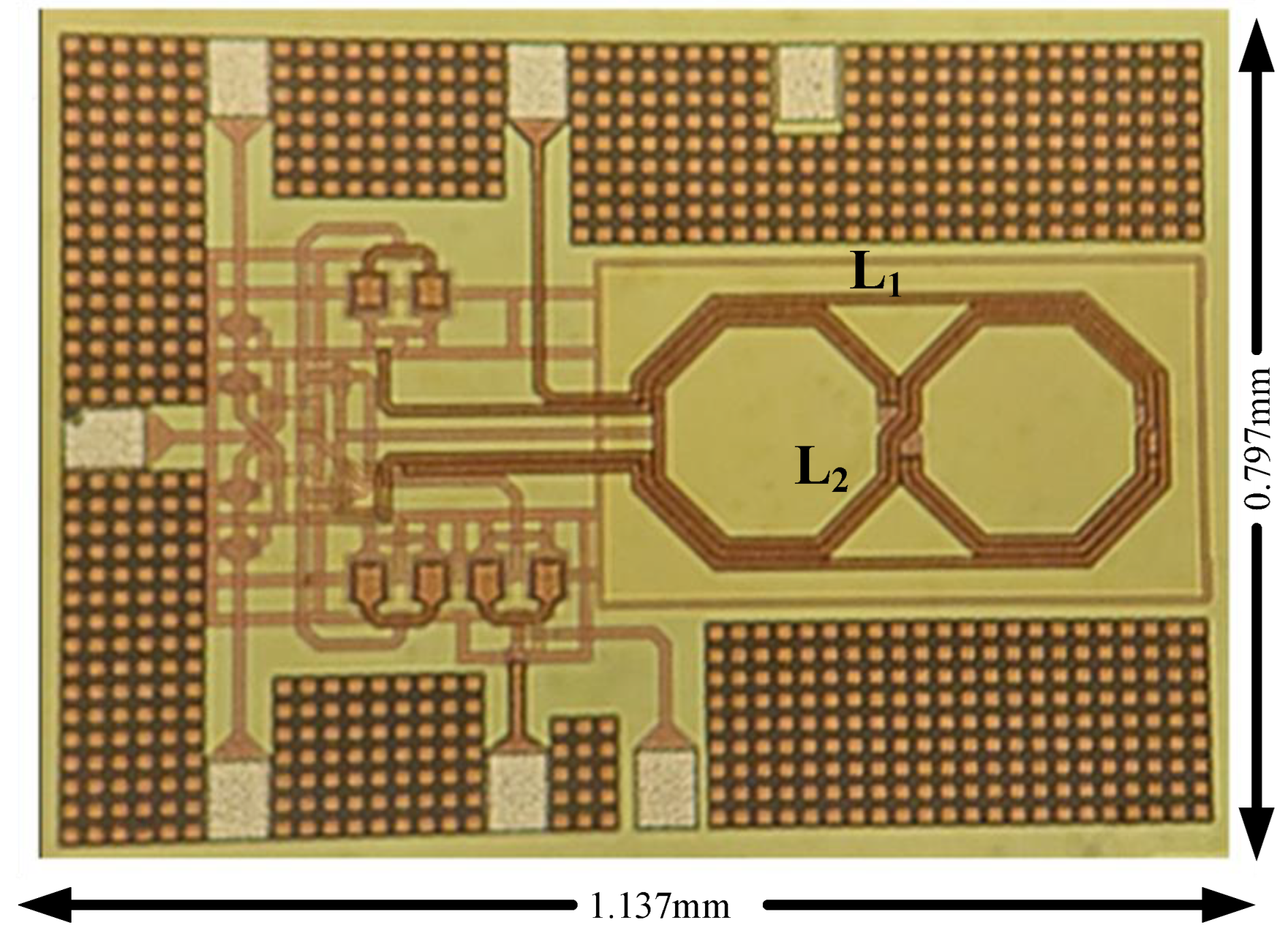
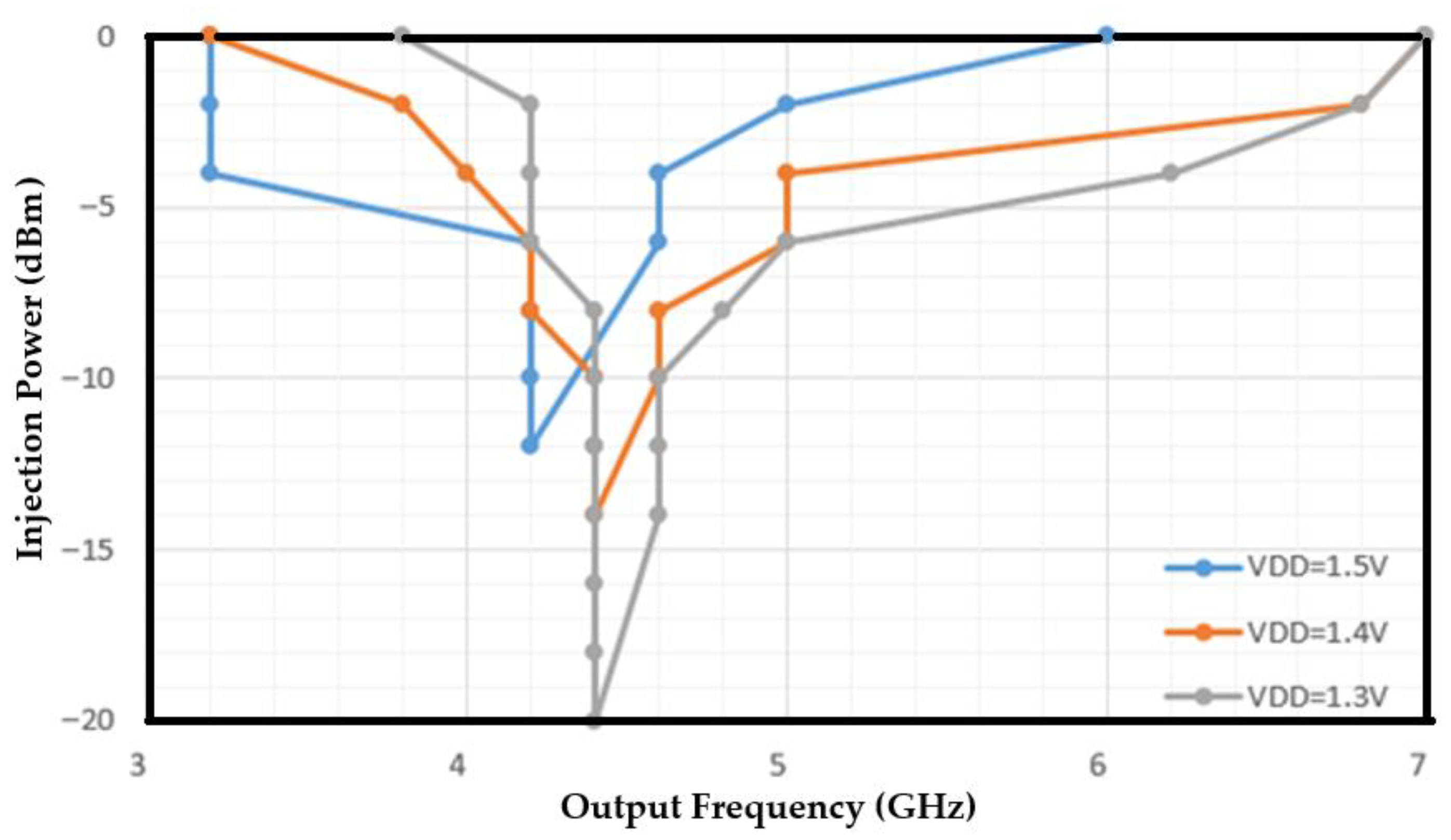
The die micrograph is shown in Figure 5. The total area, including the output buffer and the pads, is 1.137 × 0.797 mm2. At VDD = 1.5 V, the current/power consumption is 2.644 mA/3.966 mW. The setup employs a signal generator Keysight N5183A, CA, USA to provide a single-ended input signal, which is then converted to a differential signal using an external balun. The spectrum analyzer is an Agilent 4407B analyzer, CA, USA. Figure 6a shows the measured output full-span spectrum of the ×2 ILFM. The free-run output signal is at 4.27 GHz with an output power of −6.57 dBm. Figure 6b shows the measured output full-span spectrum of the ×2 ILFM under the locked condition. The output signal is at 4.2 GHz with an output power of −7.73 dBm. Figure 7 shows the measured output sensitivity of the ×2 ILFM at VDD = 1.3, 1.4, 1.5 V. At VDD = 1.3 V, the locking range is from 3.8 GHz to 7 GHz. Figure 8 shows the measured phase noises of the injection reference and the ×2 ILFM output signal. At 1/0.1/0.01 MHz offset frequency, the phase noises are −138.3/−114.94/−114.48 dBc/Hz and −133.59/−108.15/−108.09 dBc/Hz, respectively, for the input and locked output.

3. Multiply-by-3 ILFM

This section covers an ×3 ILFM with a 3-dimensional stacked orthogonal transformer, which is different from the previous ×3 ILFM [12] with a coplanar orthogonal transformer and one-band buffer filter. The ILFM can occupy a small area because the O-shaped inductor is stacked below the 8-shaped inductor. The present ×3 ILFM uses a new orthogonal transformer and buffers with dual-band filters for wide-band harmonic filtering. The present ILFM circuit uses no varactors for a wider locking range in accordance with the theory.

3.1. Circuit Design

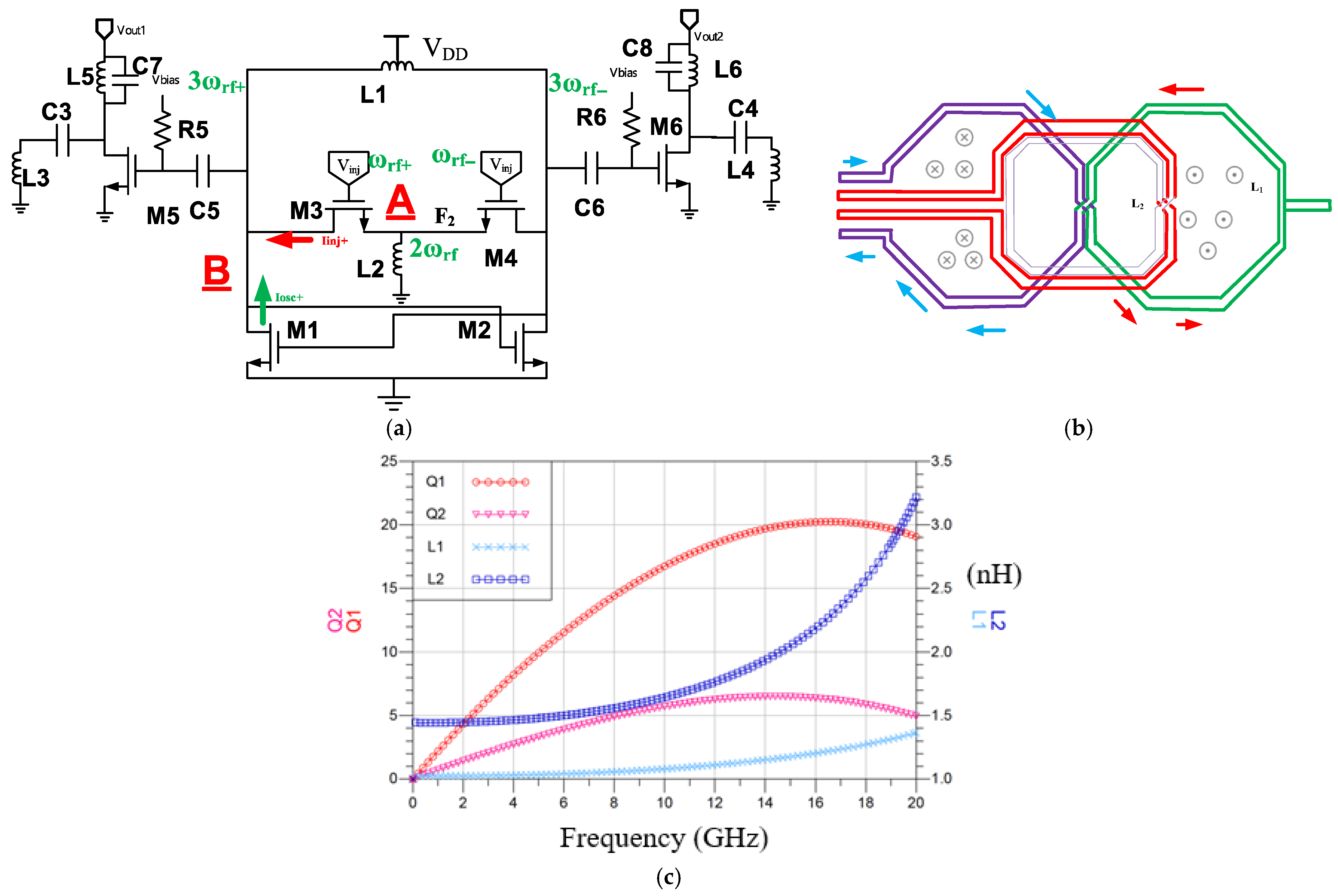
Figure 9a shows the detailed schematic of the designed ×3 ILFM. Figure 9b shows the layout of the orthogonal transformer. The lack of varactors in shunt with inductor L1 increases the locking range. One-turn eight-shaped inductor L1 is shown in Figure 9a, and parasitic varactors form the main resonator. Figure 9b also shows the layout of the orthogonal transformer. Cross-coupled nMOS (M1, M2) are negative resistor emulators. VDD is the supply voltage. NMOS (M3, M4) are injection FETs that form the frequency tripler with L2. Configuring a one-turn 8-shaped inductor L1 and a two-turn non-twisted L2 as one orthogonal transformer saves die area. FETs (M5, M6) are common-source buffers. The series-tuned filter (L3, C3) and the parallel-tuned filter (L5, C7) suppress the undesired harmonics at the buffer’s output. The input frequency is ωrf+ and ωrf-, the frequency at node A is 2ωrf, and the frequency at node B is 3ωrf+. Figure 9a differs from the circuit shown in [12], as it utilizes no tank tuning varactors, allowing the locking range to be measured.
For the ÷1 ILO with a parallel RLC resonator [13], the locking range can be written as follows:
( ω R F ω o ) = ω o I i n j 2 Q   I o s c ,
where ωo is the ILO free running oscillation frequency, ωRF is the frequency of the RF injection signal, and Q is the quality factor of the tank at resonance. Iinj/Iosc is the injection/switching drain current to the tank. The input frequency locking range [14] derived from (1) is given by
( ω R F ω o ) = g m C ,
where gm is the equivalent transconductance of the switching FET, and C is the capacitive load connected to its source and drain. The capacitance reduction leads to the locking range enhancement.
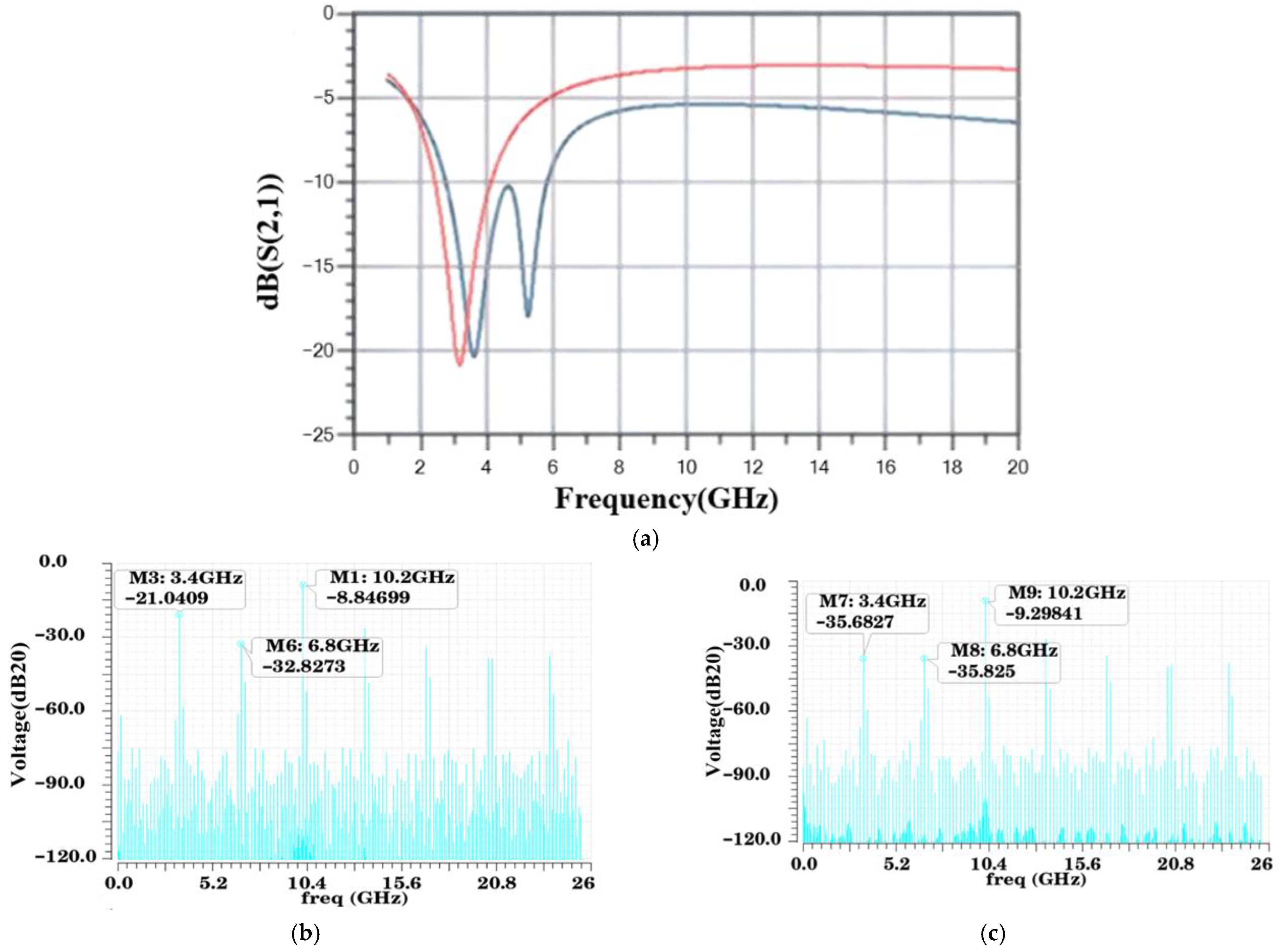
Figure 9c shows the simulated Q-factor and inductance of the transformer in Figure 9b. At 16.5 GHz, simulated inductances are L1 = 1.219 nH and L2 = 2.269 nH. Simulated Q-factors are Q1 = 20.247 and Q2 = 6.283 nH, and the coupling coefficient is 0.03. The self-resonance frequency of L1 is 37 GHz, and the self-resonance frequency of L2 is 22.5 GHz. Figure 10a shows the simulated S21 of the reference single-band filter and the implemented dual-band improved filters. It shows the simulated S21 of the output buffer filter with (L3, C3) to short the 1st harmonic and (L5 and C7) to block the 2nd harmonic from the output. Figure 10b shows a simulated full-span spectrum without a filter. Figure 10c shows the simulated full-span spectrum with a filter. The 2nd harmonic is suppressed by 2.546 dB compared to that in Figure 10b, and the 1st harmonic is further suppressed.
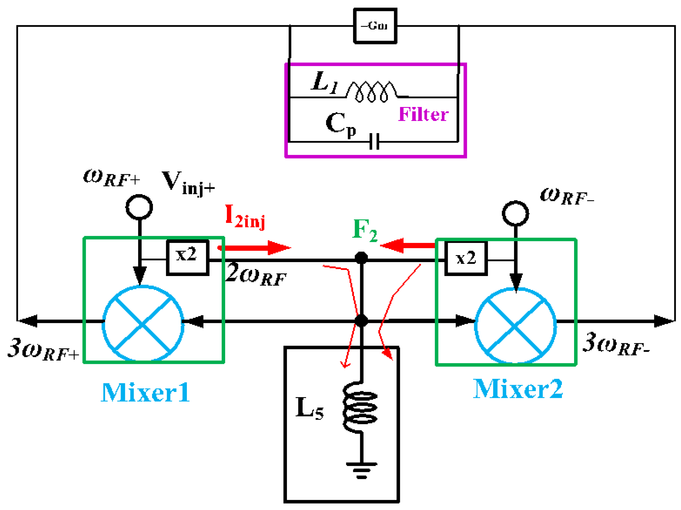
Figure 11 shows a block diagram of the ×3 ILFM. The injection FETs M3 and M4 are switched on and off cyclically. We can express the drain current id1 (id2) of M3 (M4) by memory-less nonlinear Taylor series expansion, as shown below:
i d 1 = i 0 + a 1 v gs + a 2 v gs 2 + a 3 v gs 3 + a 4 v gs 4 + ,
where vgs = A cos(ωRFt) is the fundamental gate input signal. In first order approximation, the output drain current I2inj = B cos(2ωRFt). The filter L1, parasitic capacitor Cp and −Gm form an oscillator. The mixer1 (M3)/mixer2 supplies the 2nd drain harmonic current to the inductor L5 to form a 2nd voltage at the node F2, which is a virtual ground for the odd signals. The input signal ωRF+ mixes with 2ωRF to supply an output signal 3ωRF+. The linear mixer M3 (M4) uses the input–output frequency relationship given by ωRF+ + 2ωRF = 3ωRF+, where ωRF+/3ωRF+ is the frequency of the injection signal/the frequency of the mixer output signal.

3.2. Experimental Results

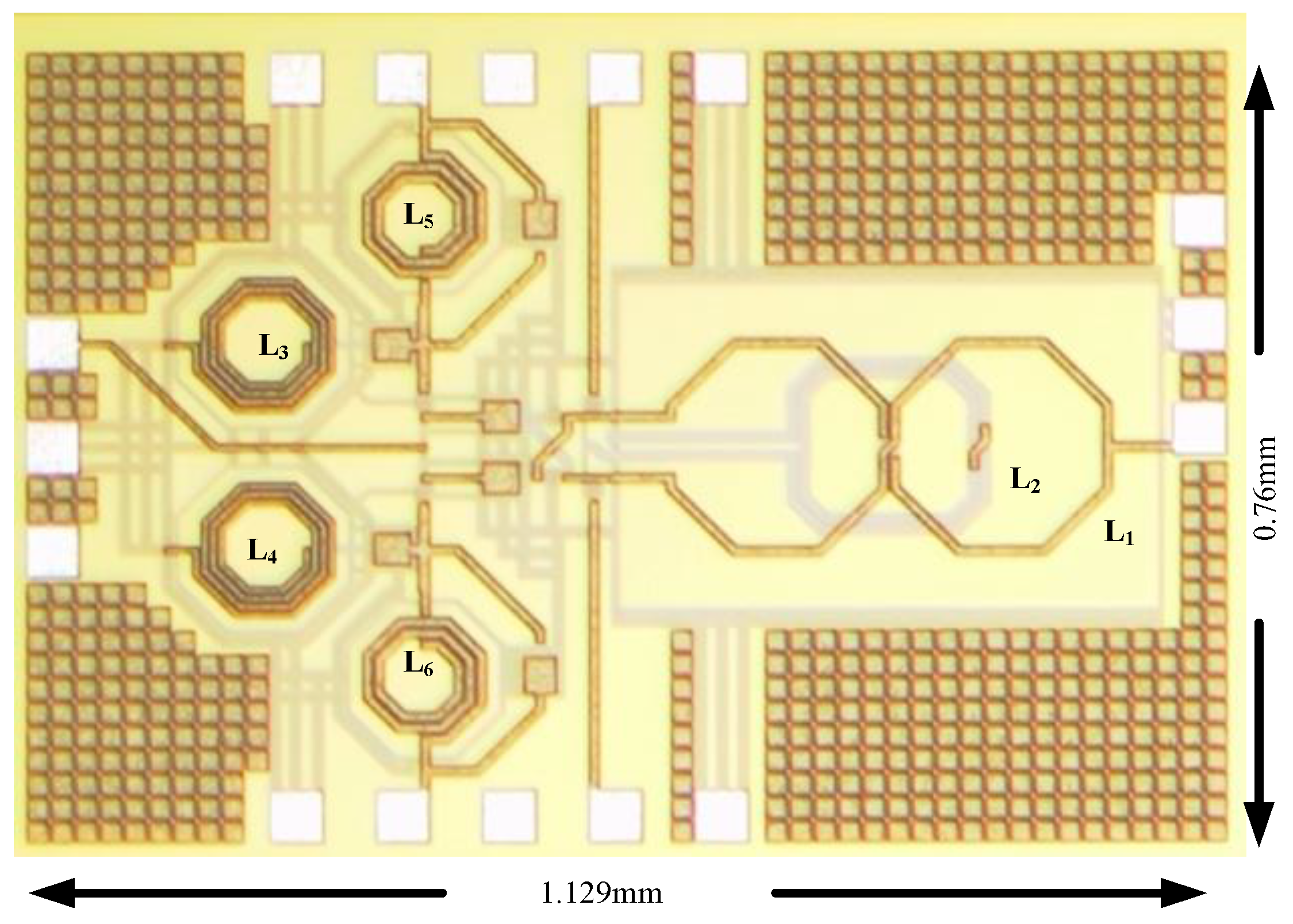
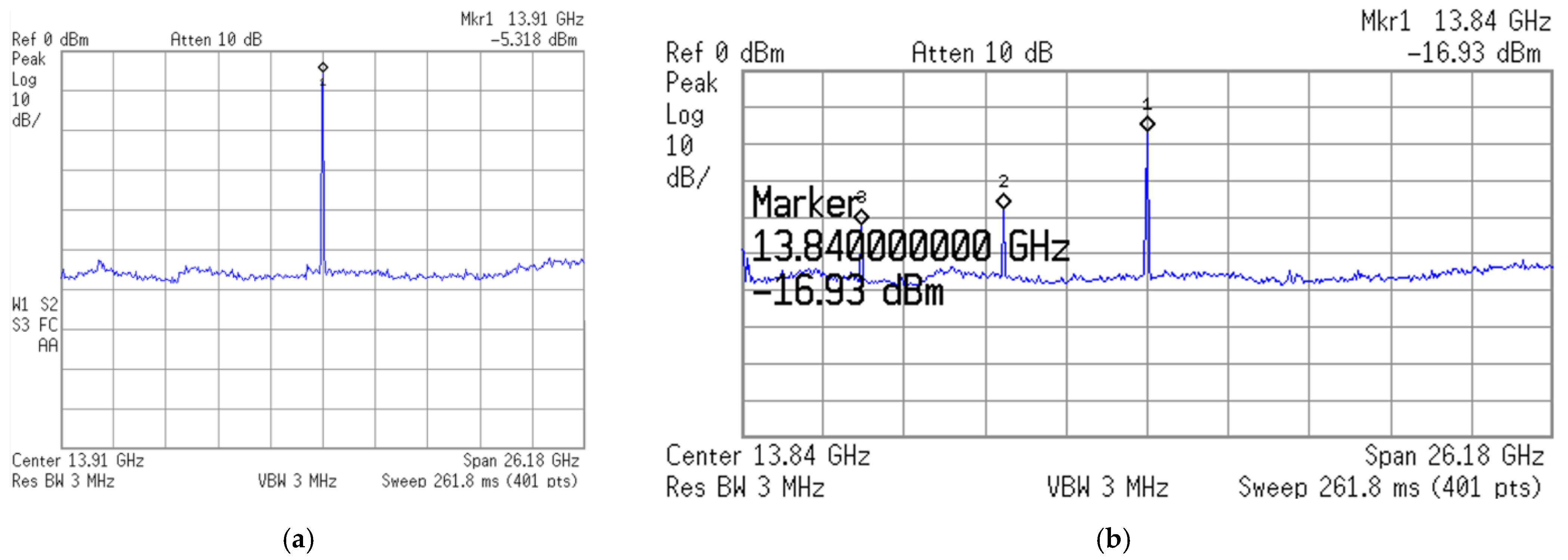
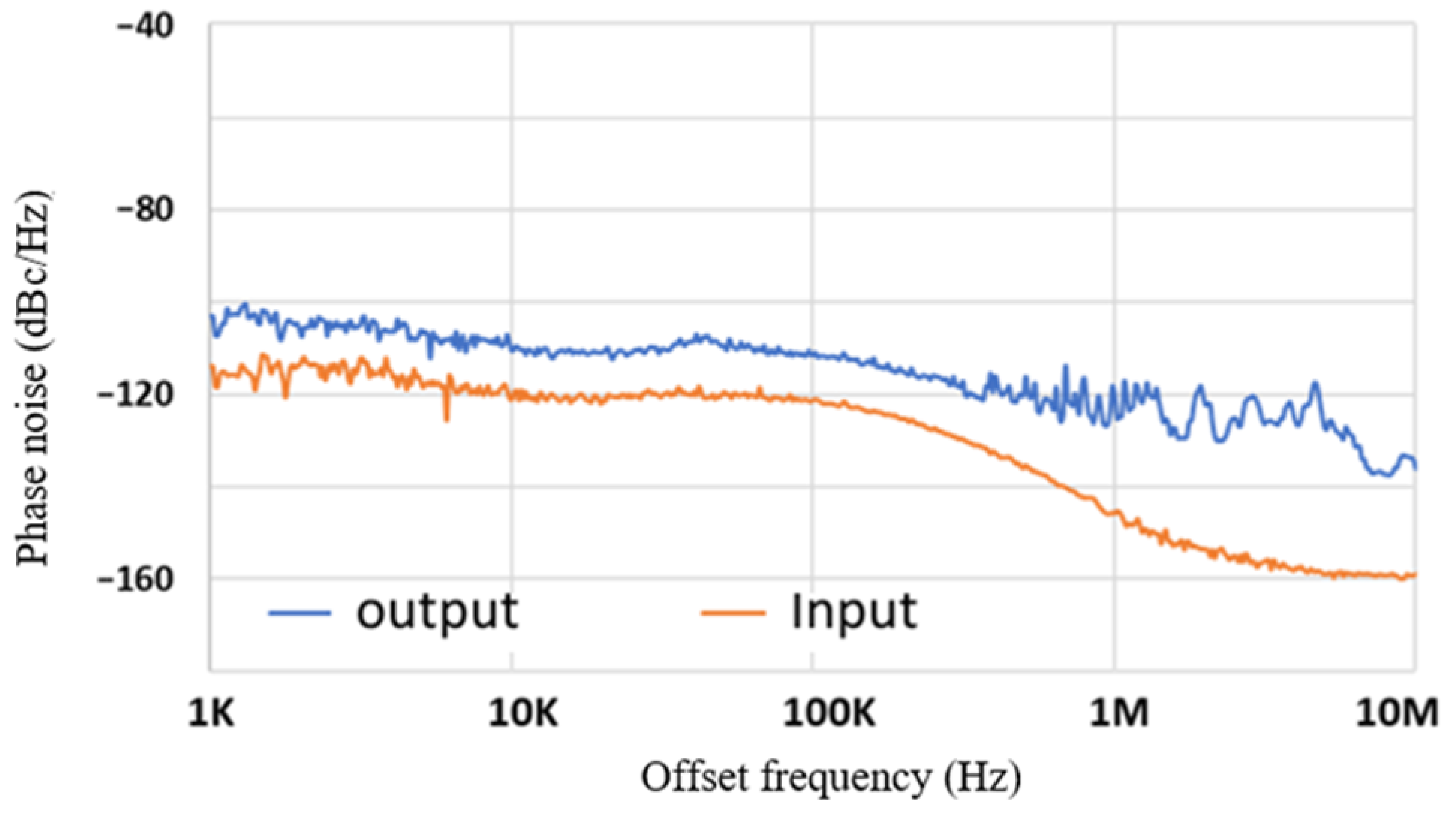
The ×3 ILFM has been designed in the TSMC 0.18 μm 1P6M CMOS technology. The die micrograph occupying an area of 1.129 × 0.76 mm2 is shown in Figure 12. Figure 13a shows the measured free-run full-span spectrum. The carrier is at 13.91 GHz and its power is −5.318 dBm. Figure 13b shows the measured locked full-span spectrum. At VDD = 0.7 V, the power consumption is 10.5 mW. The carrier is at 13.84 GHz and its power is −16.93 dBm. It contains the 1st harmonic with an output power of −37.58 dBm, the 2nd harmonic with an output power of −42.28 dBm, and the peak 3rd harmonic. Figure 14 shows the measured phase noise of the injection source at finj = 6.1 GHz. The phase noise at 1 MHz is −111.845 dBc/Hz. It also shows the measured phase noise of locked ILFT. The phase noise at 1 MHz is −103.38 dBc/Hz. At 100 K offset, the measured phase noise degeneration is close to the theoretical phase noise degeneration. At 1 M offset, the measured phase noise is beyond the theoretical phase noise and is caused by the phase noise of the free-running ×3 ILFM. Figure 15 shows the measured output sensitivity plot with different VDD. As the VDD increases, the output sensitivity plot shifts to a lower frequency.

4. Multiply-by-6 ILFM

A conventional ×6 ILF was designed with five spiral inductors. This section details a compact ×6 ILFM with one inductive component consisting of an orthogonal trifilar due to two 8-shaped inductors and one non-twisted inductor. One inductive trifilar [15] with one 8-shaped inductor was used in a power amplifier.

4.1. Circuit Design

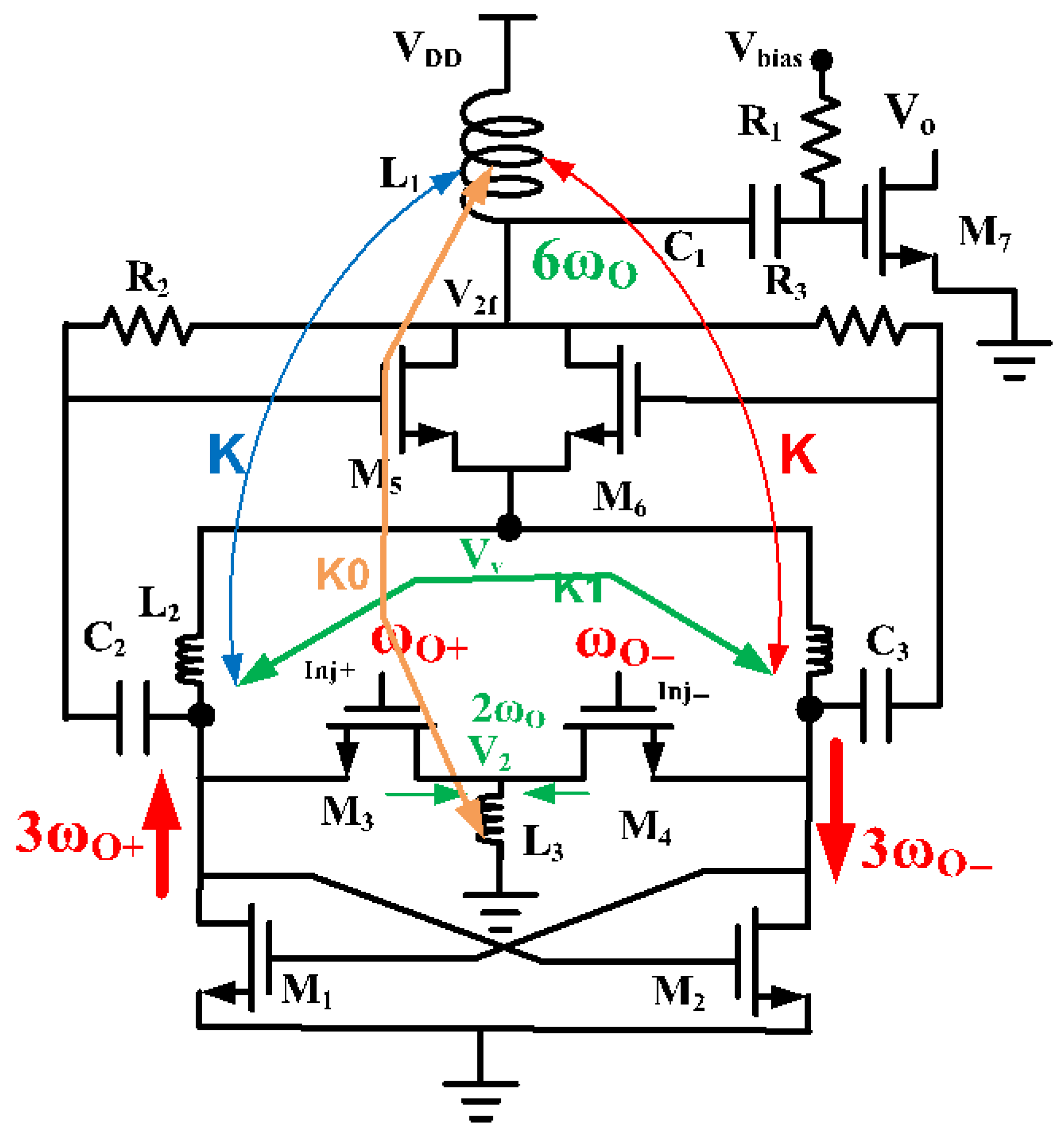
The schematic of the ×6 ILFM circuit is shown in Figure 16. The circuit block diagram of the current-reused ×6 ILFM is similar to that shown in Figure 1b. Figure 1a uses the intrinsic frequency doubler. Figure 16 uses a balanced frequency doubler. The cross-coupled nMOS transistors M1 and M2 and two-turn center-tapped 8-shaped inductors made of L2 and a parasitic capacitor form a VCO used as a first-harmonic injection-locked oscillator (ILO) with two injection nFETs M3 and M4. A differential injection signal at the frequency finj is applied to the gates of M3 and M4, with gate biasing at Vin, sharing a common non-twisted inductor L3. The common-source node Vv of M5 and M6 is a virtual ground for the fundamental signal. NFETs M5 and M6, and one-turn 8-shaped inductor L1 form the balanced frequency doubler. Transistor M7 is the output buffer for the extraction of the 6finj signal, and the locking range of the 1st harmonic ILO determines the locking range of the ×6 ILFM. Components R1~R3 are for DC biasing, and Vbias is the gate bias voltage. The nMOS VCO is used as a 1st harmonic ILO with the output oscillation frequency locked to the signal at 3finj, in case the frequency 3finj falls in the locking range of the 1st harmonic ILO. No buffer is used for the ILO; this reduces the parasitic capacitance and increases the locking range.
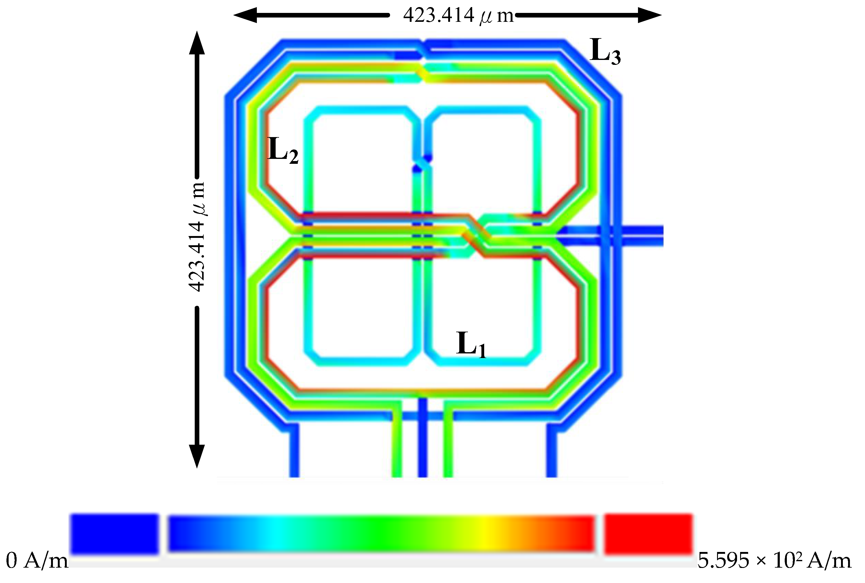
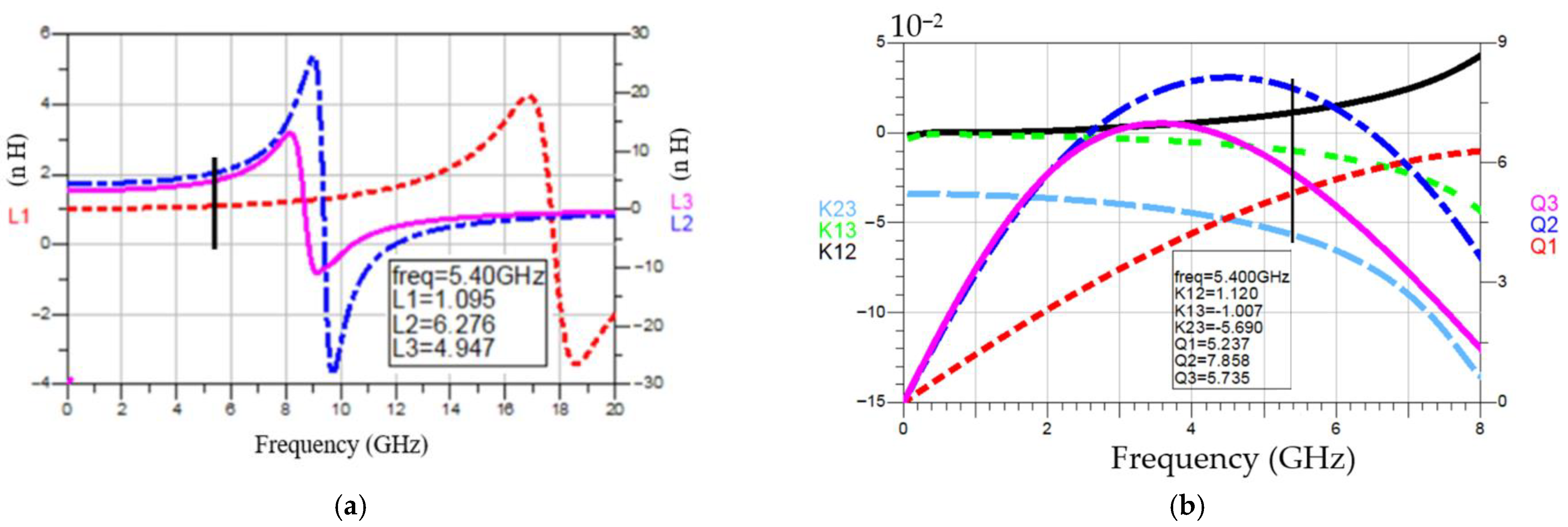
Figure 17 shows the layout of an inductive passive. The outer two-turn non-twisted inductor is L3. The inner one-turn twisted inductor is L1. The intermediate two-turn 8-shaped inductor is L2. The input of the two-turn 8-shaped inductor starts from the bottom right-hand outer turn and then goes to the left-hand inner turn of the top lobe. Figure 16 also shows the simulated current density distribution. The current at L2 is the highest. At 5.3 GHz, as shown in Figure 18, the simulated inductance of L1 (L2, L3) is 1.09 (6.17, 4.61) nH, and the simulated Q-factor of L1 (L2, L3) is 5.23 (7.85, 5.73). The simulated coupling coefficient of k12 (k13, k23) is 0.001 (0.002, 0.036), which indicates that the three inductors are almost orthogonal. The simulated self-resonant frequency of L1 (L2, L3) is 17 (9, 8.3) GHz.
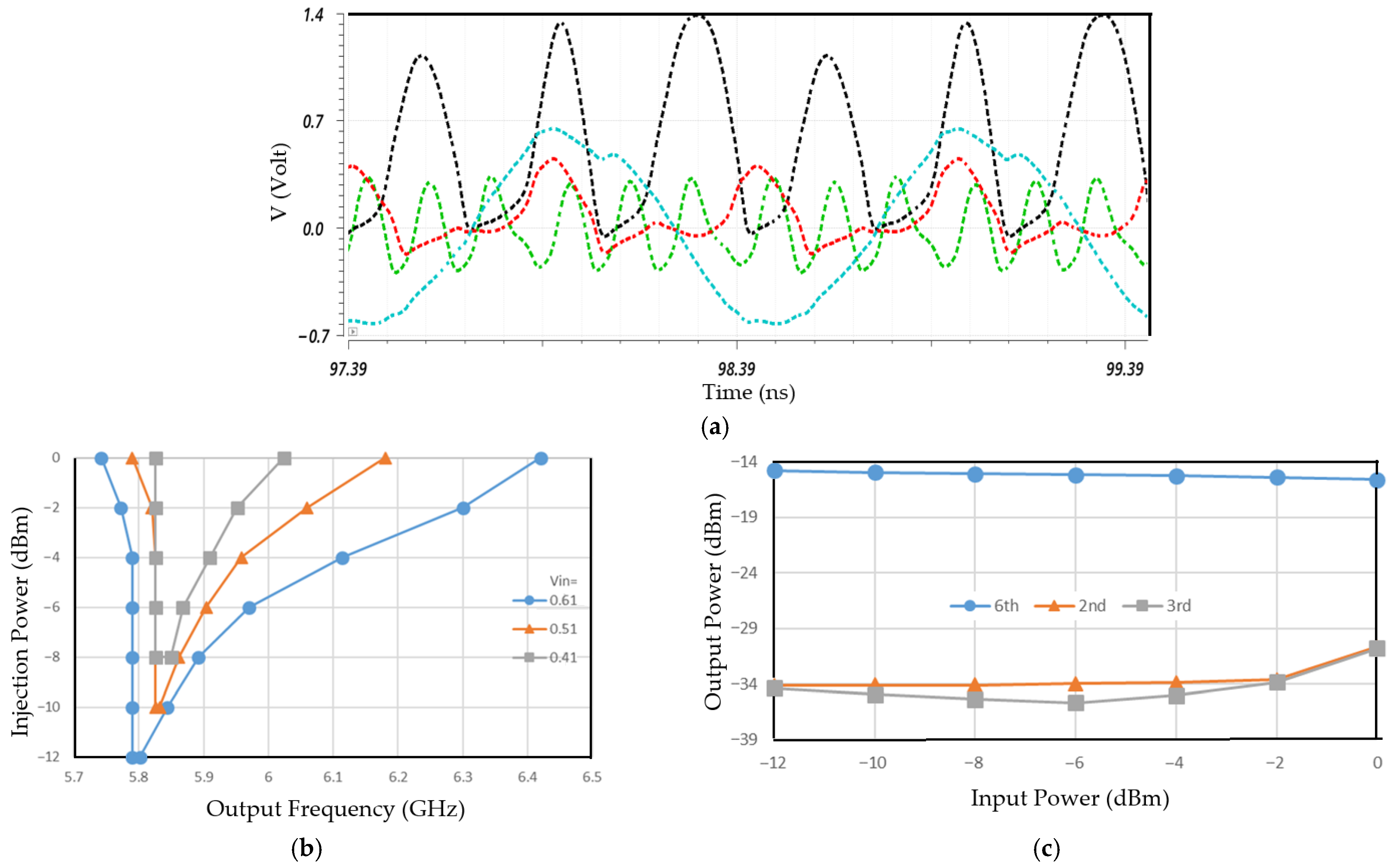
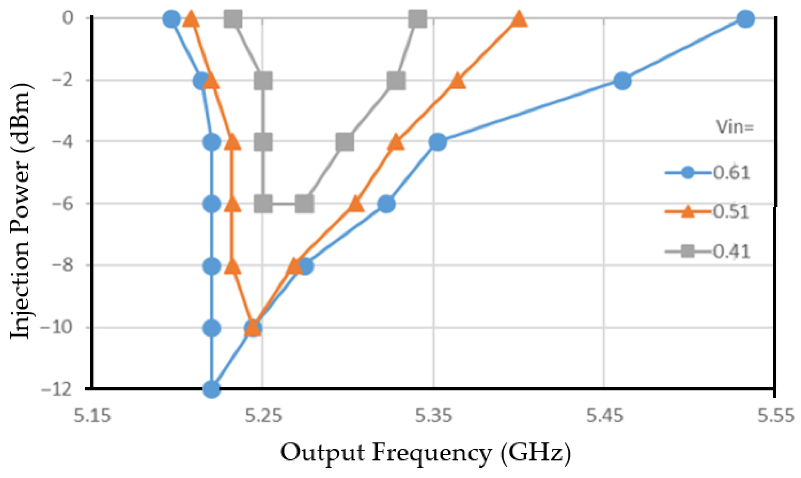
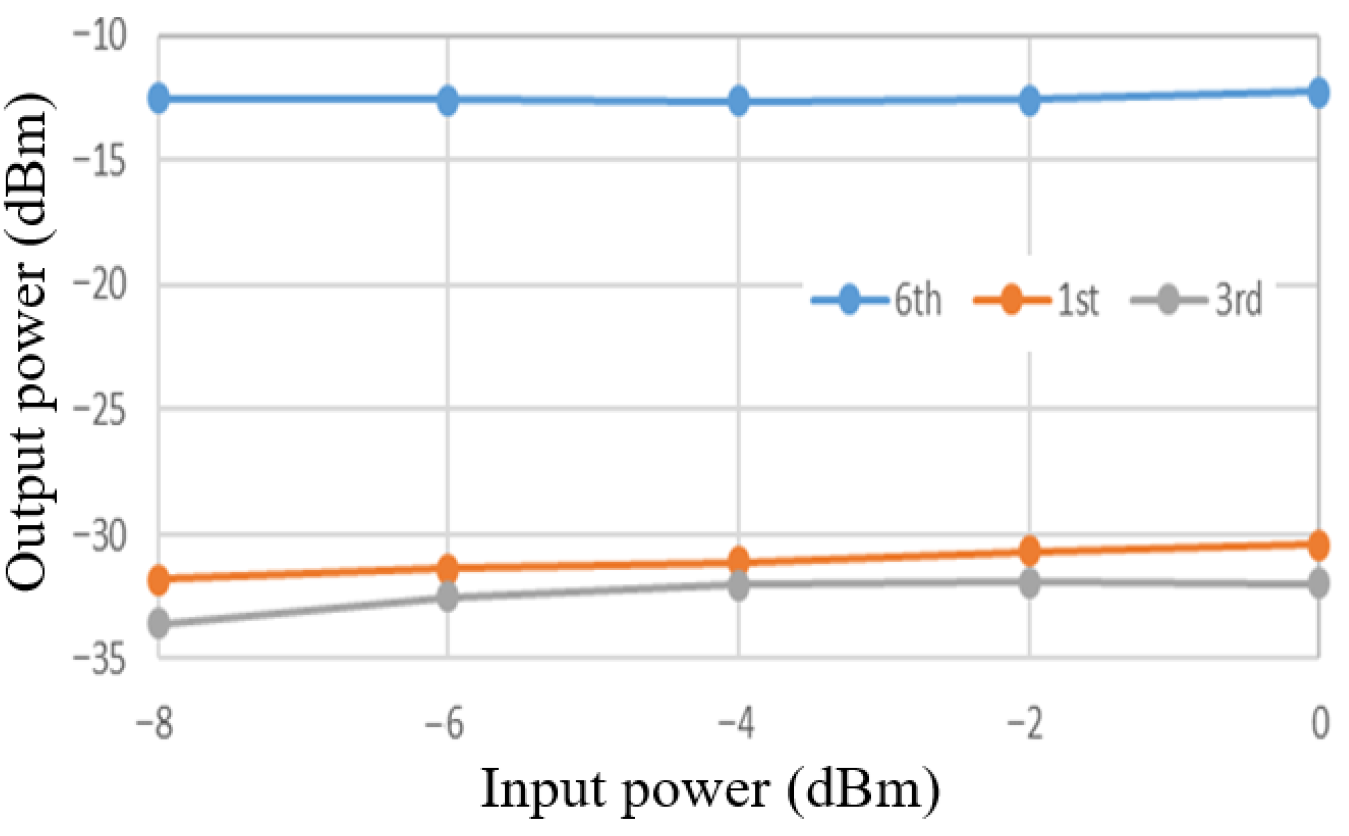
Figure 19a shows the simulated voltage waveforms under the locked condition. An injection signal is applied to the gate of M3 (M4). The frequency doubler is found at the common source of M3 and M4. The frequency tripler is found at the source of M3. The frequency sixtupler is found at the drain of M7. Figure 19b shows the simulated output sensitivity of the ×6 ILFM at three biases. The locking range at the injection gate bias Vin = 0.61 V is the largest. Figure 19c shows the simulated 6th, 2nd, and 3rd harmonic output power of the locked ×6 ILFM versus input power.

4.2. Experimental Results

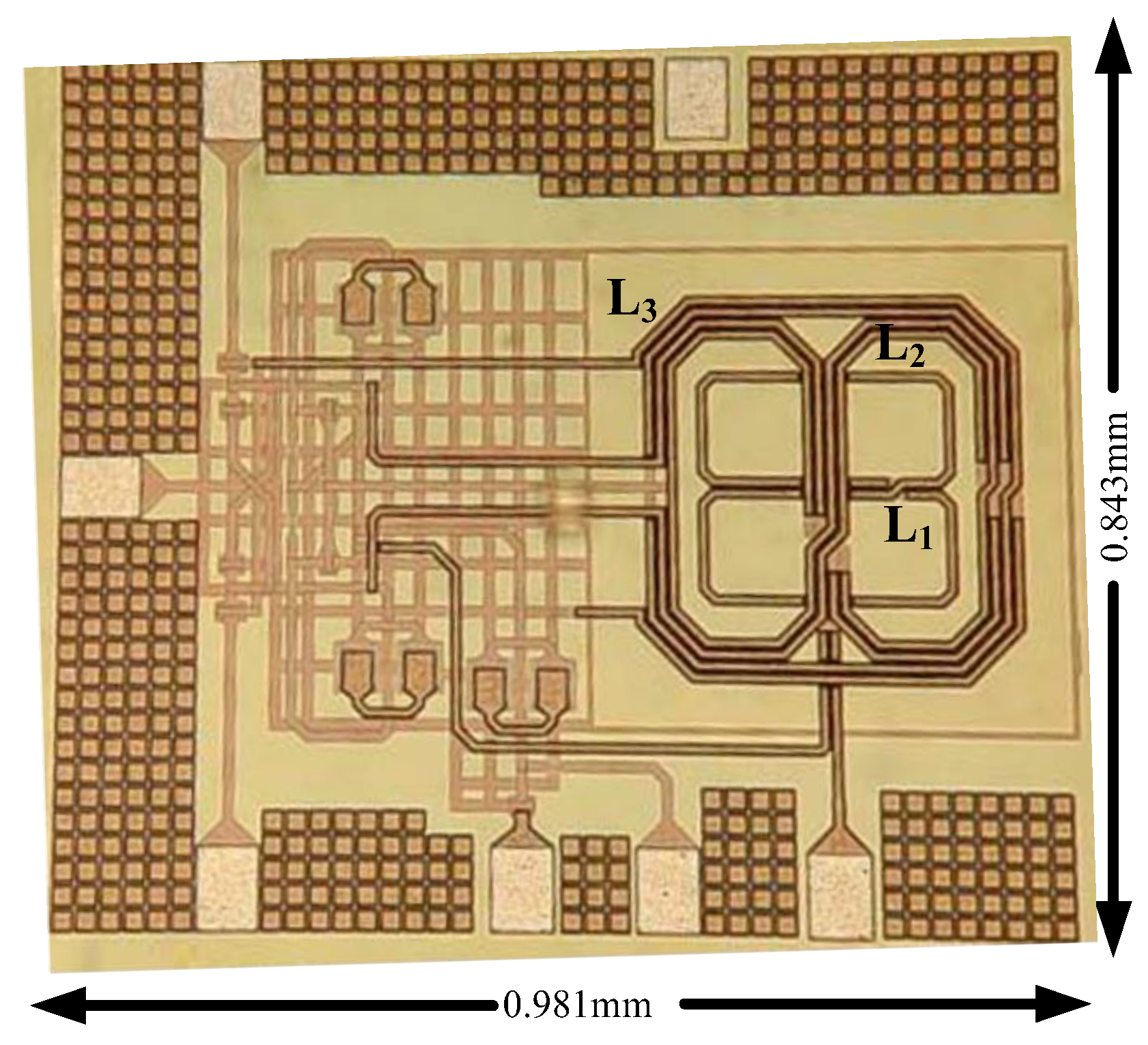
The die micrograph is shown in Figure 20. The total area, including the output buffer and the pads, is 0.843 × 0.981 mm2. At the power consumption of 13 mW, Figure 21a shows the measured free-run output spectrum of the unlocked ×6 ILFM at 5.21 GHz with an output power of −6.747 dBm. Figure 21b shows the measured free-run full-span output spectrum of the ×6 ILFM. It has the 1st harmonic at 2.65 GHz with an output power of −24.77 dBm. Figure 22a shows the measured locked output spectrum of the ×6 ILFM at 5.22 GHz with an output power of −7.318 dBm. Figure 22b shows the measured locked full-span output spectrum of the ×6 ILFM. It has a 3rd harmonic at 2.65 GHz with an output power of −23.49 dBm and a 6th harmonic at 5.22 GHz.
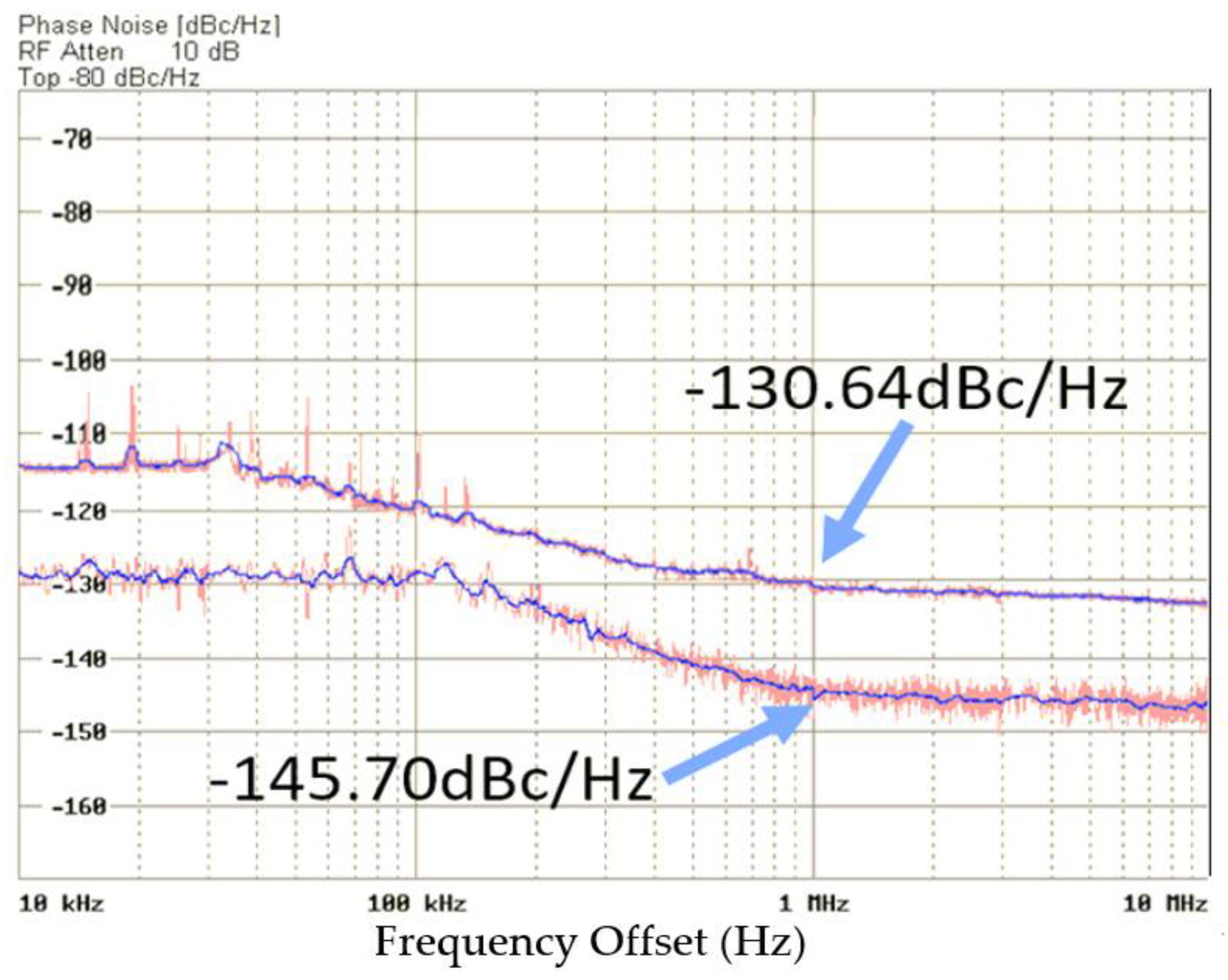
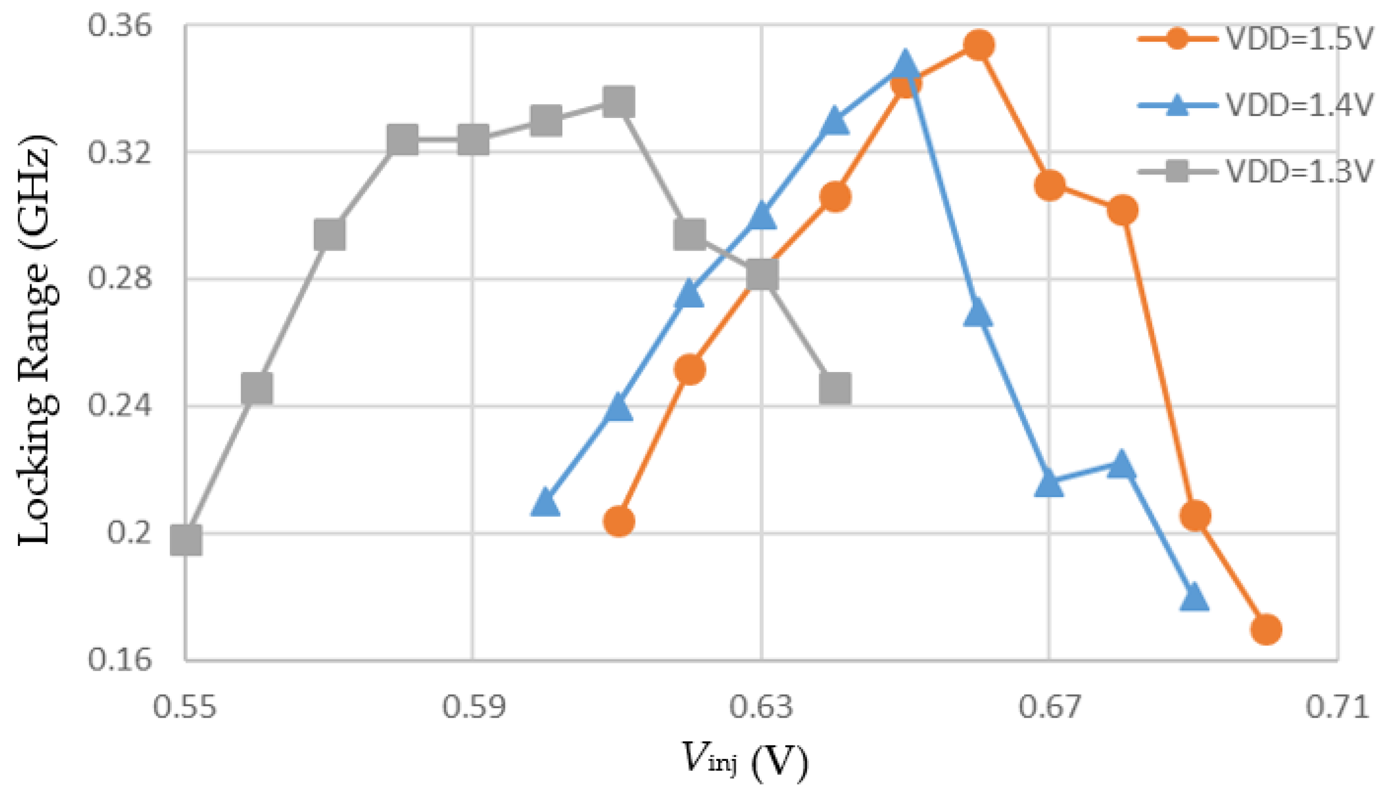
Figure 23 shows the measured phase noises of the locked ×6 ILFM at 0 dBm input power and injection reference. At 1 MHz offset, the phase noise of ILFS/injection reference is −125.87/−140.86 dBc/Hz. Figure 24 shows the measured output sensitivity of the ×6 ILFM biased at VDD = 1.3 V with the output locking range, at 0 dBm input power PINJ, from 5.16 GHz to 5.388 GHz. The locking range increases with PINJ. Figure 25 shows the measured harmonic output power of the locked ×6 ILFM at fin = 0.869 GHz; the measured harmonic output power is lower than the carrier output power by more than 17 dBm. Figure 26 shows the measured locking range output sensitivity. As VDD increases, the sensitivity plot shifts to a lower frequency. Table 1 compares the performance of the implemented ILFMs with an 8-shaped inductor against various CMOS ILFMs by using FOM = Lock Range (percent)/Power (in mW).

5. Conclusions

This paper reviews our LC-tank ILFMs with 8-shaped inductors for suppressing magnetic coupling noise, which utilize an orthogonal transformer to reduce die area. Compared to existing ILFMs, this paper utilizes single-inductor elements for the LC-tank ILFMs. The orthogonal low-k transformer was implemented in a ×2 and a ×3 ILFM, and the low-k trifilar was implemented in a ×6 ILFM to verify its function and conserve die area. All ILFMs exhibit a well-defined locking range and phase noise, and they also suppress coupling noise due to the use of an 8-shaped inductor in the ILO with a high voltage swing. The proposed inductor approach can be extended to mm-wave ILFM design.

Author Contributions

Investigation on chips 1 and 3, C.-Y.L.; Investigation on chip 2, Y.-C.L.; Writing—original draft, S.-L.J. All authors have read and agreed to the published version of the manuscript.

Funding

This research received no external funding.

Data Availability Statement

The original contributions presented in this study are included in the article. Further inquiries can be directed to the corresponding author.

Acknowledgments

The authors thank the staff of the TSRI for the chip fabrication and Meng-Ting Lin for the design of chip ×3 ILFM.

Conflicts of Interest

The authors declare no conflict of interest.

References

  1. Liu, X.; Luong, H.C. A fully Integrated 0.27-THz injection-locked frequency synthesizer with a frequency-tracking loop in 65-nm CMOS. IEEE J. Solid-State Circuits 2020, 55, 1051–1063. [Google Scholar] [CrossRef]
  2. Monaco, E.; Pozzoni, M.; Svelto, F.; Mazzanti, A. Injection-locked CMOS frequency doublers for μ-wave and mm-wave applications. IEEE J. Solid-State Circuits 2010, 45, 1565–1574.
  3. Kursu, O.; Rahkonen, T.; Pärssinen, A. A 14.6 GHz–19.2 GHz digitally controlled injection-locked frequency doubler in 45 nm SOI CMOS. In Proceedings of the 2021 16th European Microwave Integrated Circuits Conference (EuMIC), London, UK, 3–4 April 2022; pp. 104–107. [Google Scholar] [CrossRef]
  4. Jia, H.; Kuang, L.; Wang, Z.; Chi, B. A W-band injection-locked frequency doubler based on the top-injected coupled resonator. IEEE Trans. Microw. Theory Tech. 2016, 64, 210–218. [Google Scholar] [CrossRef]
  5. Iotti, L.; LaCaille, G.; Niknejad, A.M. A 57–74-GHz tail-switching injection-locked frequency tripler in 28-nm CMOS. IEEE Solid-State Circuits Lett. 2019, 2, 115–118. [Google Scholar] [CrossRef]
  6. Chang, Y.-H.; Chiang, Y.-C. A novel injection-locked frequency tripler for V-band applications. In Proceedings of the 2019 14th European Microwave Integrated Circuits Conference (EuMIC), Paris, France, 30 September–1 October 2019; pp. 290–293. [Google Scholar] [CrossRef]
  7. Jang, S.-L.; Lai, H.-W.; Sung, J.-Y.; Juang, M.-H. Injection-locked frequency tripler with boosted locking range. IEEE Microw. Wirel. Tech. Lett. 2023, 33, 423–426. [Google Scholar] [CrossRef]
  8. Jang, S.-L.; Lai, W.-C.; Lu, R.-H. Single-stage injection-locked frequency sixtupler in CMOS process. IEEE Access 2022, 10, 40316–40323. [Google Scholar] [CrossRef]
  9. Cheng, S.-J.; Shen, P.-N.; Hong, C.-H.; Chen, Z.-W.; Chen, C.-P.; Jang, S.-L. Injection-locked frequency sixtuplers in 90 nm CMOS by using the push-push doubler. IEEE Access 2023, 11, 130048–130059. [Google Scholar] [CrossRef]
  10. Jang, S.-L.; Lee, Y.-C.; Lai, W.-C. Left-Hand Resonator VCO Using an Orthogonal Transformer. Electronics 2025, 14, 2765. [Google Scholar] [CrossRef]
  11. Jang, S.-L.; Lin, Z.-J.; Juang, M.-H. State-of-the-Art VCO with Eight-Shaped Resonator-Type Transmission Line. Electronics 2025, 14, 2322. [Google Scholar] [CrossRef]
  12. Hsu, M.-H.; Jang, S.; Lin, M.-T.; Lai, W.-C.; Juang, M.-H. Differential injection-locked frequency tripler with a low-coupling 8-shaped transformer. In Proceedings of the 2024 21st International SoC Design Conference (ISOCC), Sapporo, Japan, 19–22 August 2024; pp. 388–389. [Google Scholar] [CrossRef]
  13. Razavi, B. A study of injection locking and pulling in oscillators. IEEE J. Solid-State Circuits 2004, 39, 1415–1424. [Google Scholar] [CrossRef]
  14. Takatsu, K.; Tamura, H.; Yamamoto, T.; Doi, Y.; Kanda, K.; Shibasaki, T.; Kuroda, T. A 60-GHz 1.65 mW 25.9% locking range multi-order LC oscillator based injection locked frequency divider in 65nm CMOS. In Proceedings of the IEEE Custom Integrated Circuits Conference, San Jose, CA, USA, 9–12 September 2012; pp. 1–4. [Google Scholar]
  15. Jang, S.-L.; Lin, W.-C.; Lai, W.-C.; Juang, M.-H. Area-efficient UWB CMOS power amplifier with hybrid trifilar. In Proceedings of the 2025 IEEE Wireless and Microwave Technology Conference (WAMICON), Cocoa Beach, FL, USA, 14–15 April 2025; pp. 1–4. [Google Scholar] [CrossRef]
Figure 1. (a) Schematic of the multi-inductor ×6 mm-wave ILFM. M3 and M4 are injection FETs, and Vo is the output. (b) Block diagram. FD: frequency doubler. ILFT: injection-locked frequency tripler.
Electronics 14 03360 g001
Figure 2. (a) Schematic of the injection-locked frequency doubler. (b) Block diagram.
Electronics 14 03360 g002
Figure 3. Layout of the orthogonal transformer.
Electronics 14 03360 g003
Figure 4. (a) Simulated transformer property: inductance. (b) Q-factor and coupling coefficient.
Electronics 14 03360 g004
Figure 5. Chip micrograph for the first injection-locked frequency doubler.
Electronics 14 03360 g005
Figure 6. (a) Measured free-run output spectrum of the ×2 ILFD at 4.2 GHz. VDD = 1.5 V, VOUT = 0.74 V, Vbias = 0.48 V and Vin = 0.68 V. (b) Measured locked output full-span of the ×2 ILFD at 4.2 GHz. VDD = 1.5 V, VOUT = 0.74 V, Vbias = 0.48 V, Vin = 0.68 V, fin = 2.1 GHz and Pin = 0 dBm.
Electronics 14 03360 g006
Figure 7. Measured output sensitivity of the ×2 ILFM. VDD = 1.3, 1.4, 1.5 V, VOUT = 0.74 V, Vbias = 0.48 V and Vin = 0.68 V.
Electronics 14 03360 g007
Figure 8. Measured phase noises of the locked ×2 ILFM at 0 dBm input and injection reference.
Electronics 14 03360 g008
Figure 9. (a) Schematic of the ×3 ILFM. (b) The layout of the transformer shows the current and magnetic field directions. L1 is in the metal M6 layer. L2 is in the metal M5 layer. (c) Simulated inductance and Q-factor.
Electronics 14 03360 g009
Figure 10. (a) Simulated S21 of the red single-band filter and the blue dual-band improved filters. (b) Simulated full-span spectrum without filter. (c) Simulated full-span spectrum with filter.
Electronics 14 03360 g010
Figure 11. Block diagram of the ×3 ILFM. −Gm is the transconductance of the oscillator.
Electronics 14 03360 g011
Figure 12. Chip micrograph.
Electronics 14 03360 g012
Figure 13. (a) Measured free-run full-span spectrum. VDD = 0.7 V, Vin = 0.4 V, Vbias = 0.9 V and Vbuf = 1.5 V. (b) Measured locked spectrum. finj = 6.1 GHz.
Electronics 14 03360 g013
Figure 14. Measured phase noise of the injection source. finj = 6.1 GHz and VDD = 0.7 V. Measured phase noise of locked ×3 ILFM.
Electronics 14 03360 g014
Figure 15. Measured output sensitivity plot. Vin = 0.7 V, Vbias = 0.9 V, Vout = 1.5 V, VDD = 0.7, 0.75 and 0.8 V.
Electronics 14 03360 g015
Figure 16. Schematic of the injection-locked frequency sixtupler. Coupling coefficients can be ignored.
Electronics 14 03360 g016
Figure 17. Layout of inductive passive with current density distribution. Input condition: L1: 0.54 V at 5.4 GHz, L2: 1.44 V at 2.7 GHz and L3 = 0.24 V at 1.8 GHz.
Electronics 14 03360 g017
Figure 18. (a) Simulated inductance, (b) Q-factor, and K-factor.
Electronics 14 03360 g018
Figure 19. (a) Simulated voltage waveforms. VDD without the bonding wire effect. VDD = 1.3 V, Vinj = 0.58 V, Vbias = 0.8 V and VOUT = 1 V. Input: blue. Frequency doubler: red. Frequency tripler: black. Frequency sixtupler: green. fin = 0.958 GHz, Pin = 0 dBm. (b) Simulated output sensitivity of the ×6 ILFM. VDD = 1.3 V, VOUT = 0.43 V, Vbias = 0.8 V and Vin = 0.41, 0.51, 0.61 V. (c) The simulated harmonic output power of the locked ×6 ILFM versus input power.
Electronics 14 03360 g019
Figure 20. Chip micrograph for the ×6 ILFM.
Electronics 14 03360 g020
Figure 21. (a) Measured free-run output spectrum of the ×6 ILFM. (b) Measured output full-span of the free-run ×6 ILFM. finj = 0 MHz; Pinj is off.
Electronics 14 03360 g021
Figure 22. (a) Measured locked spectrum of the ×6 ILFM. (b) Measured output full-span of the ×6 ILFM. finj = 870 MHz; Pinj = 0 dBm.
Electronics 14 03360 g022
Figure 23. Measured phase noise of the locked ×6 ILFM at 0 dBm input and injection reference. VDD = 1.3 V, VOUT = 0.43 V, Vbias = 1.19 V and Vin = 0.61 V. fin = 0.87 GHz and Pin = 0 dBm.
Electronics 14 03360 g023
Figure 24. Measured output sensitivity of the ×6 ILFM. VDD = 1.3 V, VOUT = 0.43 V, Vbias = 1.19 V and Vin = 0.41, 0.51, 0.61 V.
Electronics 14 03360 g024
Figure 25. Measured harmonic output power of the locked ×6 ILFM at VDD = 1.3 V, VOUT = 0.43 V, Vbias = 1.19 V, Vin = 0.61 V and fin = 0.869 GHz. The carrier: blue. The red: 2nd harmonic. The gray: 3rd harmonic.
Electronics 14 03360 g025
Figure 26. Measured locking range sensitivity of the ×6 ILFM versus Vinj at VDD = 1.3, 1.4, 1.5 V, VOUT = 0.43 V, Vbias = 1.19 V, Pin = 0 dBm GHz.
Electronics 14 03360 g026
Table 1. Performance comparison of standalone CMOS LC ILFMs.
Ref. ×2Tech
(nm)
Inductor
Structure
Pin
(dBm)
Vdd(V) Pdis(mW)Die Area
(mm2)
FOMLocking Range
(GHz)
[4] TMTT 2016 ×265Spiral tran01/90.39 × 0.413.271~95.0 (28.9%)
[3] EuMIC 2022 ×245Spiral indu01/5–110.124.55~14.0~17.6 (22.78%)
[2] JSSC 2010 ×265Spiral indu31/60.0142.18106~128 (13.1%) *
[12] ISOCC 2024 ×31808-sha tran00.65/3.251.146 × 0.484 10.75 **7.2~10.25 (34.95%) **
[9] Access 2023 ×690Spiral indu00.4/9.030.491.1339~43.2 (10.21%)
[8] Access 2022 ×6180Spiral indu01/20.81.141 × 1.20.49475.62~6.23 (10.29%)
This 1 ×21808-sha tran01.5/3.9661.137 × 0.79715.3473.2~6 (60.96%) *
This 2 ×31808-sha tran00.7/10.51.129 × 0.767.143~6.6 (75%) ***
This 3 ×61808-s trifilar01.3/130.843 × 0.981 0.33255.16~5.388 (4.32%)
FOM = lock range (percent)/ power (in mW). * Output frequency locking range. ** with frequency tuning. *** Input replaces output locking range. This (1, 2, and 3) refer to the three different frequency multiplier (×2, ×3, ×6).
Disclaimer/Publisher’s Note: The statements, opinions and data contained in all publications are solely those of the individual author(s) and contributor(s) and not of MDPI and/or the editor(s). MDPI and/or the editor(s) disclaim responsibility for any injury to people or property resulting from any ideas, methods, instructions or products referred to in the content.