Article

On the SCA Resistance of TMR-Protected Cryptographic Designs

1
IHP—Leibniz-Institut für Innovative Mikroelektronik, 15236 Frankfurt (Oder), Germany
2
Chair of Wireless Systems, Institute of Computer Science, Faculty 1: Mathematics, Computer Science, Physics, Electrical Engineering and Information Technology, Brandenburg University of Technology Cottbus-Senftenberg, 03046 Cottbus, Germany
*
Author to whom correspondence should be addressed.
Electronics 2025, 14(16), 3318; https://doi.org/10.3390/electronics14163318
Submission received: 1 July 2025 / Revised: 6 August 2025 / Accepted: 14 August 2025 / Published: 20 August 2025
(This article belongs to the Special Issue Advances in Hardware Security Research)

Abstract

The influence of redundant implementations on success of physical attacks against cryptographic devices is currently under-researched. This is especially an issue in application fields such as wearable health, industrial control systems and the like in which devices are accessible to potential attackers. This paper presents results of an investigation of the TMR application impact on the vulnerability of FPGA-based asymmetric cryptographic accelerators to side-channel analysis attacks. We implemented our cryptographic cores using full- and partial-TMR application approaches and experimentally conducted evaluation of their side-channel resistance. Our results reveal that TMR can significantly impact side-channel leakage, either increasing resistance by introducing noise or amplifying leakage depending on the part of the design where redundancy was applied.

1. Introduction

With the advent of the Internet of Things, electronic devices are becoming ubiquitous in almost all fields of application ranging from wearable health care via industrial control systems and critical infrastructures to space missions. What these applications have in common are that the devices—at least to some extend—are physically accessible, i.e., devices can be physical manipulated and/or analysed by attackers. In addition, these applications require extreme reliability and that majority of the data are sensitive, meaning their integrity and confidentiality are of utmost importance. The latter two features are ensured using cryptographic approaches; reliability can be achieved by redundancy, e.g., triple modular redundancy.
The influence of redundant implementations on physical attacks against cryptographic devices is currently under-researched and frankly speaking rather unknown. On the one hand, redundancy is a suitable means to countermeasure fault injection attacks. On the other hand, it might increase the leakage exploited in side-channel attacks. In this paper, we are researching exactly this relation. Our primary goal is to explore the impact of triple modular redundancy on the attack’s success against a cryptographic implementation of asymmetric approaches. Therefore, we decided to use our own design due to the fact that it was extensively investigated in our previous work. The design is a hardware accelerator for elliptic curve (EC) point multiplication, which is the main operation in all EC-based cryptographic protocols. The design is vulnerable to address-bit attacks, and the leakage source is a key-dependent addressing of registers.
We extended our own design applying the TMR strategy for different design blocks, ported it to an FPGA and captured electromagnetic radiation traces which we used to run side-channel attacks to extract the used key.
Our main contributions are summarized as follows.
  • We presented the first detailed experimental results of the impact of triple modular redundancy (TMR) on side-channel resistance of FPGA-based asymmetric cryptography designs.
  • We demonstrated that TMR can both reduce and amplify SCA leakage depending on design factors such as selective redundancy application.
  • We provide guidelines for hardware designers aiming at balancing fault tolerance and side-channel resistance.
The rest of this paper is organized as follows: Section 2 reviews the current state of research on side-channel attacks targeting TMR-protected designs. Section 3 introduces the tools and methodologies used for automated implementation of TMR. Section 4 describes our cryptographic designs selected for evaluation and how TMR was applied. Section 5 presents the experimental setup, conducted attack as well as a discussion of the attack results. Finally, Section 6 concludes the paper and presents our plans for future work.

2. SCA Attacks Against TMR: State of the Art

Traditional countermeasures against fault injection attacks are based on techniques that allow detection and coping with injected faults, preventing them from affecting the outputs or leaking sensitive data. These techniques are based on redundancy application, e.g., dual-, triple-, or n-modular redundancy, error detection and correction codes. Countermeasures against fault injection attacks are under-investigated in the context of side-channel analysis attacks. There is a limited number of papers that shed light on how a countermeasure designed for one type of attack might influence the effectiveness of the other. Some of them are briefly discussed below.
In 2007/2008, authors of [1,2] assumed that a countermeasure against fault injection attacks may have an impact on the resistance of a cryptographic implementation. Using VHDL they implemented S-boxes for the AES and Kasumi ciphers and modified them by adding parity check circuits. To verify their assumption, authors conducted correlation power analysis attack against traces simulated for the UMC [3] 180 nm technology. For their implementation with parity check circuits, the number of key bits found was increased by up to 38% for the Kasumi algorithm and by up to 45% for AES compared to the implementations without fault detection circuits. Authors also demonstrated in [2], that application of error detection circuits can be beneficial for attackers in case of noisy measurements.
In [4] correlation power analysis was conducted against power traces measured on a SASEBO-GII (equipped with a Virtex-5 FPGA) board for an AES protected by different error detection schemes. These included cyclic redundancy check (CRC) codes, as well as duplicated critical components. The results demonstrated that all implemented protection circuits made the design more vulnerable to correlation power analysis (CPA) attacks. The performed CPA attack against the AES implementation with protection using duplication of critical components had a similar success rate as the unprotected original version. This was explained by the authors as a consequence of the signal-to-noise ratio (SNR) being almost unaffected when both leakage and noise are doubled.
In [5,6] authors investigated how fault detection methods affect the resistance of an AES implementation against correlation power analysis. As target platform, authors used a Sakura-G board [7] with a Xilinx Spartan-6 FPGA. Power traces of the AES implementations with double modular redundancy (DMR), inverse function and parity check code were captured using ChipWhisperer for identical keys and plaintexts. The authors demonstrated that fault detection techniques applied for different design blocks have different impact on the design’s resistance. For instance, parity applied to the S-Box increased the design’s resistance to CPA, while DMR and inverse function reduced the resistance, making the key recovery faster. The authors also discovered that applying more fault detection schemes to other design modules does not help to protect the implementation from the CPA attack and can actually help attackers. The impact of fault detection schemes on CPA resistance varies and some may unintentionally weaken security.
The authors of [8] wanted to investigate how the application of modular redundancy affects the resistance of an AES 128 implementation. The implemented design was based on the application of DMR, TMR as well as NMR, i.e., they used multiple copies of the same AES module. Measurements were conducted by using a PicoScope 6404D portable oscilloscope on the Evariste III platform equipped with an Altera Cyclone III FPGA. Unfortunately, the paper provides no results of the attack.
In [9], the same authors made another attempt to evaluate the resistance to differential power analysis (DPA) of AES implementations protected by fault-tolerant techniques based on parity check, space and time redundancy. They implemented five designs with fault-tolerant techniques and compared them to the standard design. The designs were synthesized for 1 MHz clock frequency targeting the Evariste III platform [10,11]. Power traces were captured using an Agilent DSO 7104A oscilloscope for each of the implementations. Authors demonstrated that in most of the cases, application of fault-tolerant techniques had minimal impact on the design, while slightly increasing its resistance against DPA.
Authors of [8] continued their work on the topic and published a paper [12] in which they proposed a masked duplex architecture for the Present cipher [13], compared it with an TMR implementation and evaluated the SCA leakage based on Welch’s test [14] applied to 1 million traces. Authors do not observe significant difference in leakage between the single and the TMR implementation of the design. In the case of the proposed masked duplex architecture, there was a significant leakage. However, authors managed to eliminate it using alternative comparison logic.
In [15], the effectiveness of side-channel analysis attacking AES implementations with triple modular redundancy is investigated. Authors implemented three instances of the same design applying TMR—the implementation with three identical AES blocks without optimization, its optimized version and, finally, the instance where TMR was achieved by using three structurally different functionally equivalent AES implementations. Design instances were synthesized for a 500 MHz clock frequency and a 65 nm technology library. For each of the investigated designs authors simulated power traces for 1000 random plaintexts with a simulation step of 1 ns, resulting in 2 simulated values per clock cycle. The conducted CPA attack was based on Pearson’s correlation coefficient. The authors pointed out that the application of TMR brought no benefits for their first two instances of TMR designs compared to the single AES design. However, an attack against the third instance, where physically and structurally different AES designs were applied for TMR implementation, resulted in increased computational efforts required to reveal the secret key. In general, the last one is obvious, as any two of these three AES blocks in the TMR implementation act as a noise source from the third block perspective.
While different studies have analyzed the effect of TMR on cryptographic circuits (mostly AES implementations), their findings vary significantly. Some of them report enhanced resistance to side-channel attacks, while others indicate increased vulnerability. As a result, there is no clear, unambiguous conclusion regarding whether redundancy schemes like TMR strengthen or weaken the resistance of cryptographic implementations against SCA attacks.

3. Tools for Automated Triple Modular Redundancy Implementation

As circuits become more complex, manual logic redundancy implementation in large-scale hardware designs may become time-consuming and error-prone. Therefore, usage of automated tools for TMR/NMR implementation becomes essential in modern HDL-based designs. The number of such tools is quite limited. Most of the industrial-grade TMR tools, such as Synopsys Synplify Premier [16] or Siemens Precision Hi-Rel [17], are proprietary and require commercial licenses, and at the same time may be vendor-specific or suitable to a dedicated FPGA family only, e.g., the Xilinx TMRTool [18]. However, there are still a few free, open-source alternatives available such as BL-TMR [19] developed at the Brigham Young University (BYU) under the support of the Los Alamos National Laboratory, SpyDrNet/SpyDrNet TMR—a format independent tool for netlist transformation developed at BYU Configurable Computing Lab [20,21].
We made our choice in favor of SpyDrNet TMR (version 1.14) due to the facts that it is a free, open-source, python-based framework with an intuitive API for accessing, analyzing and modifying generic netlist data structures. The documentation provides all the installation instructions and tutorials required for quick start as well as examples for Digilent boards.
In this work, we investigated several possibilities for TMR implementation, i.e., implementation of the entire design using triplicated logic, as well as partial TMR application for implementation of critical blocks selected to be protected. We followed the design flow illustrated in Figure 1.
The starting point of the flow is an original HDL-based implementation of a design.
The module to be implemented using the TMR logic is independently synthesized as a new project to generate a netlist. After this step, the synthesized netlist of a selected block can be exported as an EDIF (used in this work) or Verilog netlist formats, both compatible with SpyDrNet. The next step is a netlist modification using the SpyDrNet python script that replicates the logic three times and inserts majority voters at appropriate output nodes. Then, the resulting TMR netlist is encapsulated into an IP core to be instantiated within the original design, maintaining design hierarchy. The original design is updated to include the pre-synthesized TMR IP core. The rest of the steps follow the regular Vivado [22] design flow, i.e., the complete design is synthesized, passed through implementation stages including placement, routing, and timing analysis. Finally, a bitstream is generated.

4. Investigated Designs

4.1. Original Design

The starting point of the investigations conducted in this work is a hardware accelerator of an Elliptic Curve point multiplication (kP operation) for the standard NIST elliptic curve B-233 [23] with the irreducible polynomial f(t) = t233 + t74 + 1. The kP operation in B-233 was selected as example for the investigations and due to the fact that the resistance of the accelerator to horizontal SCA attacks was well investigated in the past [24,25]. The implementation is described using VHDL language, based on the modification of the Montgomery kP algorithm [26] with Lopez–Dahab coordinates. The implemented algorithm is given in the Appendix A (Algorithm A1). For more implementation details see FPGA1 design in Section 7.2 of [27]. Here, we try to avoid a detailed explanation of the algorithm so as to focus on the investigation of how triplication of different design blocks influences its resistance to SCA.
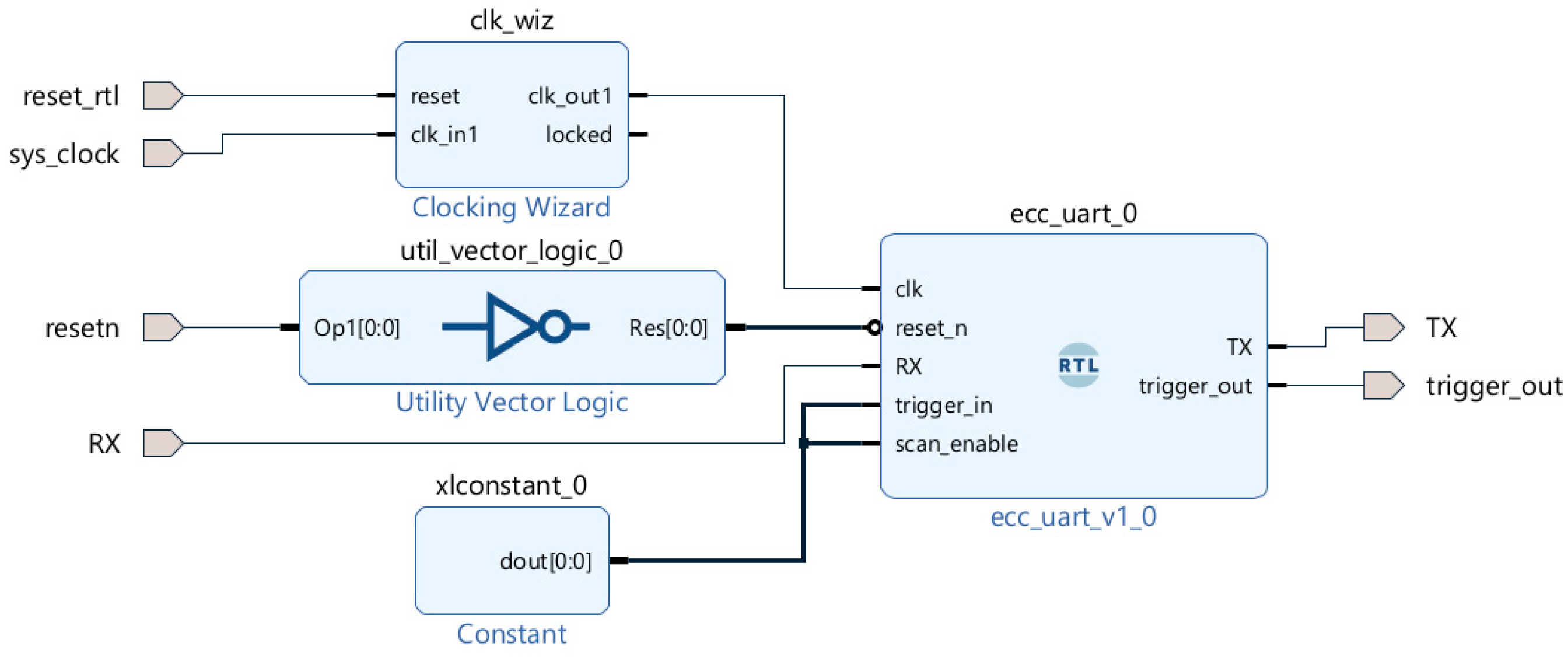
The selected target platform is a Digilent Arty Z7-20 development board [28] with a Xilinx Zynq 7020 FPGA. The original design, denoted as Design_0 in the rest of the paper, was synthesized and implemented using Vivado v2022.1 (64-bit, SW Build: 3526262) with “Vivado Synthesis Defaults” and “Vivado Implementation Defaults” strategies for a clock frequency of 10 MHz. The block diagram of the implemented design is shown in Figure 2.
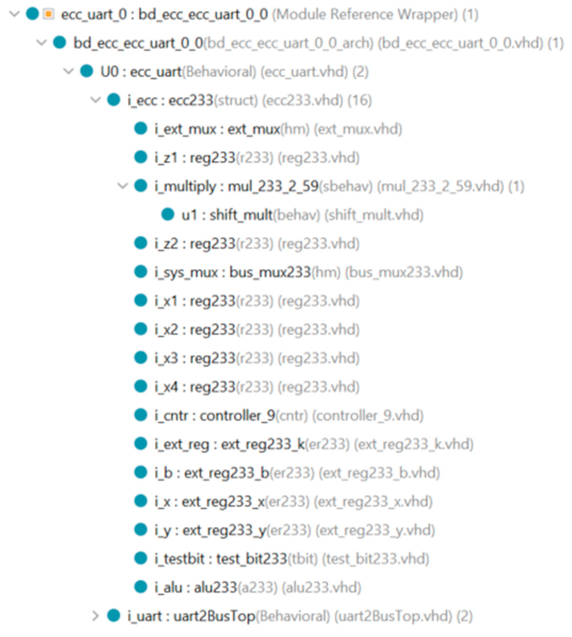
The kP accelerator requires an up to 233-bit long binary scalar k as well as affine coordinates x and y of a point P as inputs. The output is represented by two coordinates—the result of a scalar multiplication of the value k with a point P. The communication with the design is performed using a UART interface represented by RX/TX ports in the diagram. The hierarchy of the ecc_uart_0 block is shown in Figure 3. The main block implementing the kP operation is called i_ecc.
The part of the design responsible for the kP operation consists of the following main components:
  • controller (i_cntr)—manages the sequence of the field operations and data flow between the rest of the components;
  • arithmetic logic unit (i_alu)—performs squaring or addition of operands;
  • multiplier (i_multiply)—calculates the field product of 233-bit-long operands using 9 partial products according to a fixed calculation plan [26], implemented according to the iterative 4-segment Karatsuba multiplication method;
  • partial multiplier (u1)—calculates partial products for the multiplier, implemented using only the classical multiplication formula [29];
  • 233-bit-long registers: for the implementation of the main loop of the algorithm (i_x1, i_x2, i_x3, i_x4, i_z1, i_z2), input/output registers (i_x, i_y), and the registers that hold the value of scalar k and the parameter b of the elliptic curve equation (i_ext_reg, i_b);
  • muxer (i_sys_mux)—ensures data exchange between design components.

4.2. TMR Instances of the Original Design

Following the design flow represented in Figure 1, we created several instances of the original design with the goal of investigating the impact of triple module redundancy application on the design’s vulnerability to side-channel attacks:
  • Design_1: contains a multiplier (i.e., the i_multiply component) implemented using TMR;
  • Design_2: triple modular redundancy was applied to six registers used in the main loop of the algorithm, i.e., registers i_x1, i_x2, i_x3, i_x4, i_z1, i_z2;
  • Design_3: combines the components implemented using TMR logic in Design_1 and Design_2 (i.e., the multiplier and six registers);
  • Design_4: the i_ecc part of the ecc_uart_0 block (see Figure 3), responsible for the calculation of the kP operation was implemented using TMR logic.
The result of triplication is shown schematically on the example of the i_z1 register in Figure 4.
As can be seen, each flip-flop from the original design was triplicated with a shared voter inserted for the Design_2 and Design_3. Implementation of i_z1 register in Design_4, follows the same scheme employing TMR with distributed voters (i.e., three voters for three flip-flops) since the triplication of the register occurred as a part of the triplication process of its parent module i_ecc.
The FPGA resource utilization for investigated designs is given in Table 1. A more detailed table providing a hierarchical comparison of resource usage is given in the Appendix (Table A1).

5. SCA Attack and Results Discussion

5.1. Measurements

The board was placed in the Langer ICS 105 IC scanner [30] equipped with a Langer MFA-R 0.2-75 near-field probe [31] that allows precise measurements of high-frequency near fields close to the board components. According to the board schematic [32], the measurement point should be selected close to one of the power decoupling capacitors C125—C134 for internal core supply voltage VCCINT. However, the board lacks reference designators—only a small part of components can be matched to the schematic. For this reason we selected the capacitor with the best signal-to-noise ratio for the measurements experimentally. The exact placement of the probe is illustrated in Figure 5.
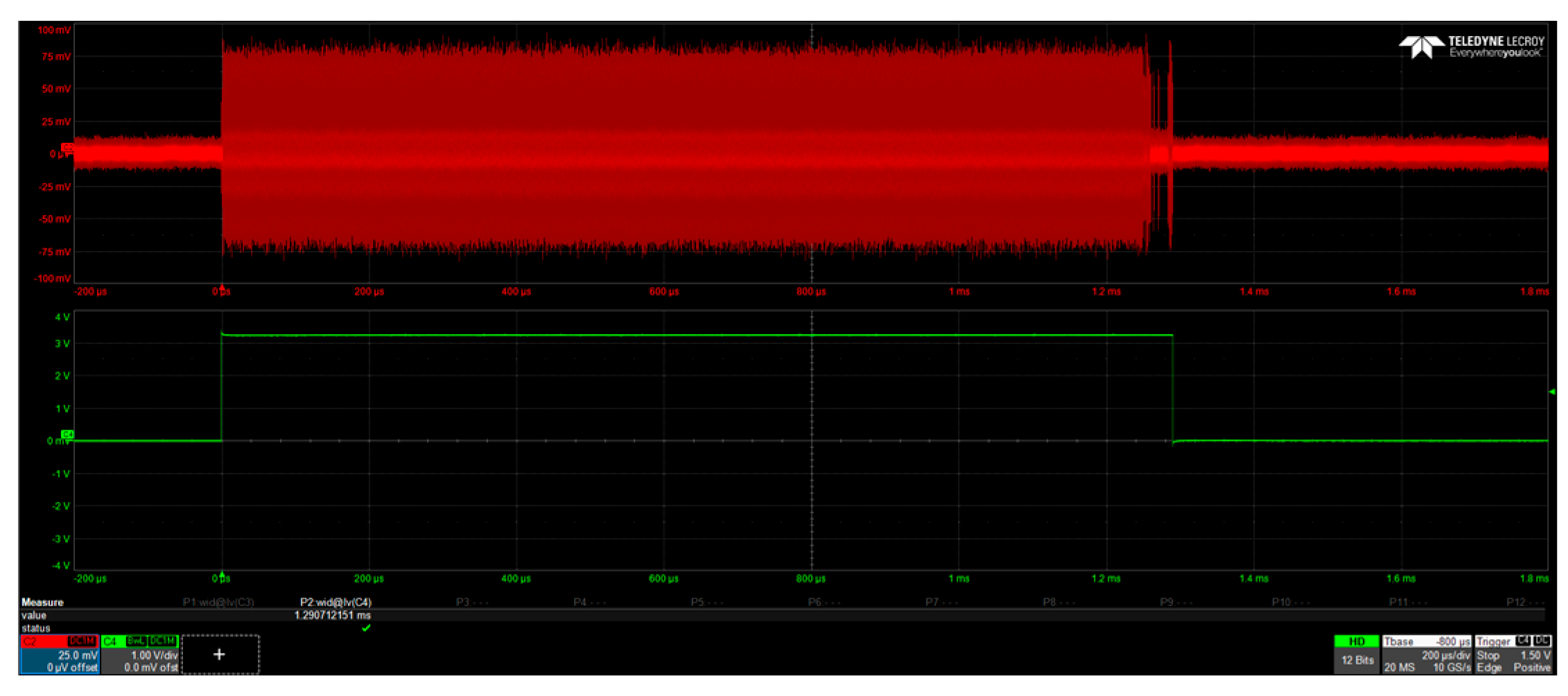
Five electromagnetic traces, one for each of the attacked designs, were captured during the execution of kP operations using a WavePro 254HD (Teledyne LeCroy GmbH, Heidelberg, Germany) oscilloscope [33], operating at a sampling rate of 10 GS/s. The placement of the EM probe as well as the inputs for the kP implementation were kept constant for all investigated cases. The design’s functionality and the correctness of the kP calculation were verified by validating the output result. A screenshot of the captured EM trace for the original design is given in Figure 6.
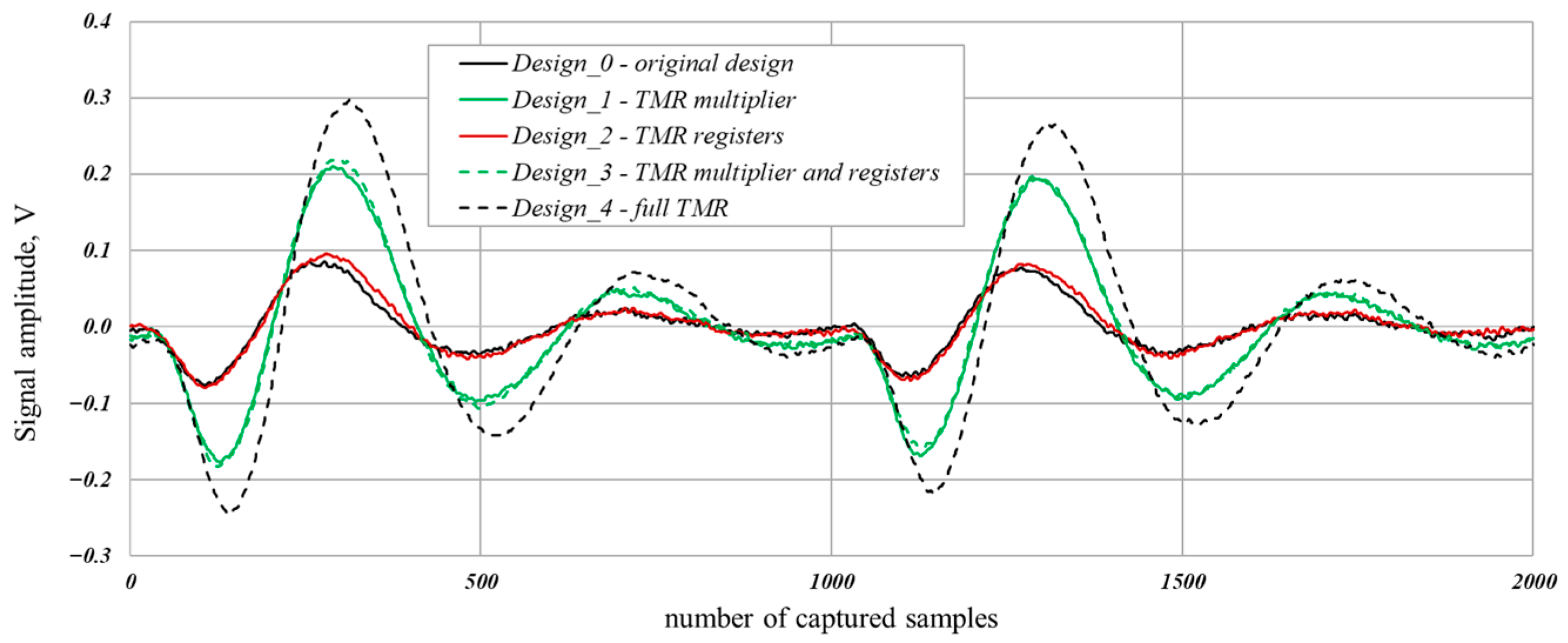
The captured EM traces differ in the signal amplitude depending on the design’s instance. For example, the trace for the Design_4 with the full TMR has about three times higher signal amplitude compared to the original Design_0 without TMR. The difference in signal amplitude is demonstrated on parts of the synchronized traces depicted in Figure 7.
It can be seen in Figure 7 that the application of the TMR influences not only the amplitude of the signal but also the signal propagation delays. As TMR introduces additional logic paths and voters, it alters the timing of signal transitions. These changes in propagation delays affect the alignment and duration of switching activity, thus influencing the shape of captured EM traces and detectability of SCA leakage.

5.2. Performed Attack

The conducted attack is described in detail in [27,34]. It is suitable for implementations in which computations are performed in a sequence of steps corresponding to individual bits of a secret scalar, e.g., algorithms with bitwise processing of a scalar in the elliptic curve scalar multiplication. Each of these steps is referred to as a “slot”, representing a fixed-length period of time during which one bit of the scalar is processed. The attacker’s goal is to reveal the value of each bit processed in these slots by analyzing the corresponding power consumption or electromagnetic emanation trace. In other words, an attacker exploits statistical differences in power consumption between parts that process ‘0’ key bits and those that process ‘1’ key bits, under the assumption that these two sets have distinguishable mean shapes in the corresponding power or electromagnetic traces.
Although the attacker does not know the processed scalar (i.e., has no knowledge of which slot corresponds to which bit value) as well as the exact operation performed in each slot, he can calculate a mean slot over all slots. This mean slot is then used as a reference for comparison. By comparing the shape of each individual slot to the shape of the mean slot sample-wise, the attacker attempts to classify the bit value of that individual slot. For example, if a sample from a slot is lower (or higher) than the corresponding point in the mean trace, the bit is classified as a ‘0’ bit, based on the assumption that less power is consumed (or vice versa). Two hypotheses are considered: one where ‘0’-slots consume less power on average than ‘1’-slots, and the other where the opposite is true.
Application of this classification to all slots results in a sequence of key candidates. Because the two hypotheses are inverses of one another, only one needs to be applied for extracting key candidates and inverted key candidates can be applied to assess the attack success, too.

5.3. Attack Results and Discussion

As our designs operate at 10 MHz and the sampling rate during the measurements was set to 10 GS/s, a single clock cycle is represented by 1000 captured samples. We compressed the trace by applying the sum of absolute values to represent each clock cycle using a single value.
Due to the fact that the processing of a single key bit in our implementation requires 54 clock cycles only, we obtained 54 key candidates. All key candidates were compared to the real key by calculating the Hamming distance HD of each key candidate and the real key, which is the scalar k processed, and the relative correctness δ using the following equation:
δ = 1 H D k e y _ l e n g t h · 100 %
The results of the attack against the original design as well as its four instances employing triple modular redundancy are presented graphically in Figure 8.
As can be seen, for Design_4 (see dashed black line), in which the TMR was applied to the whole design, most of the key candidates have a correctness similar to the one of the original implementations without redundancy (see blue line for Design_0). The best key candidate (key candidate 41) has a correctness of 99.5% for Design_4, while the maximum correctness of 99.1% is achieved for the candidate with the same index in the original, i.e., Design_0. These results were quite expected, as the impact of power consumption related to the TMR application is increased proportionally for all design blocks. However, some of the key candidates have significantly increased (e.g., key candidates 21, 40, 41, 45, 48) or reduced (key candidate 44) correctness compared to the original design. This may be caused either by differences in signal propagation delays that originate from TMR application or placement and routing steps of the design implementation.
The usage of registers in the design is key-dependent, see steps 11, 12 and 14, 15 in the Algorithm A1. Therefore, the power consumed by accessing these registers contributes to side-channel leakage responsible for the key revealing. By triplicating only the registers in Design_2, we expected an increase in this leakage. Attack results confirm this assumption (see red line in Figure 8)—most of the key candidates have an increased correctness compared not only to the original design, but to the full TMR design as well. This is the one instance out of the investigated ones that achieved the highest correctness of 100% (key candidate 41), meaning that the key candidate is equal to the original key.
The field multiplier is the biggest and most energy-consuming unit in our design, which is active in all clock cycles during main loop iterations. This means that the rest of the operations, including those that are key-dependent, are performed in parallel to multiplications. The multiplier block is resistant to the performed horizontal attack [24]. Thus, the multiplier acts as an inherent noise source in the design, which can hide the key-dependent activity of other blocks, thereby increasing the design’s resistance to SCA attacks [27]. The implementation of the multiplier block using TMR in Design_1 significantly increases the level of noise produced by the design, resulting in considerably reduced correctness of the keys revealed (see green solid line in Figure 8). Most of the key candidates have a correctness below 75% while the best key candidate has a correctness of 79% (key candidate 39).
Design_3 (see green dashed line), that includes triplicated registers and field multiplier blocks, shows slightly increased vulnerability compared to the Design_1 (see green dashed line). Again, the correctness is increased due to the increased power consumed by the registers, which contributes to the SCA leakage.
Our results demonstrate that a sophisticated TMR approach is crucial for enhancing the side-channel resistance of cryptographic designs. Designers have to understand how much each part of their implementation leaks information as well as what is the source of the noise and apply TMR to the noise source blocks such as field multipliers rather than simply triplicating everything without a clear strategy.

6. Conclusions and Future Work

Our experiments demonstrate that TMR affects side-channel resistance of cryptographic implementations. Selective redundancy added to functional blocks of the design can make SCA attacks either more successful and easier to perform or reduce the design’s vulnerability, introducing a sufficient amount of noise to hide leakage sources. Thus, although TMR application may provide protection under specific conditions, it should not be considered a primary countermeasure against SCA attacks. Furthermore, application of TMR can unintentionally increase SCA leakage, potentially weakening the security of otherwise resilient designs.
In our future work we plan to investigate the impact of TMR on the success of attacks by exploiting static currents, including those conducted under laser illumination or operating parameters variation.

Author Contributions

Conceptualization, I.K. and Z.D.; funding acquisition, P.L.; investigation, I.K.; methodology, I.K. and Z.D.; software, I.K.; validation, I.K.; writing—original draft, I.K.; writing—review and editing, I.K., P.L. and Z.D. All authors have read and agreed to the published version of the manuscript.

Funding

This research received no external funding.

Data Availability Statement

The data presented in this study are available on request from the corresponding author.

Conflicts of Interest

The authors declare no conflicts of interest.

Abbreviations

The following abbreviations are used in this manuscript:
AESAdvanced encryption standard
CPACorrelation power analysis
CRCCyclic redundancy check
DPADifferential power analysis
DMRDouble modular redundancy
SNRSignal-to-noise ratio
TMRTriple modular redundancy

Appendix A

Algorithm A1: Modified Montgomery algorithm for the kP operation corresponding to [27]
Input: k = (kl−1 … k1 k0)2 with kl−1 = 1, P = (x,y) is a point of EC over GF(2l)
Output: kP = (x1, y1)

1: X1 ← x,    X2 ← x4 + b,   Z2 ← x2 //initialization
2: if kl−2 = 1 then   //processing second most significant bit
3: T ← Z2,   Z1 (X1Z2 + X2)2, X1 ← X1Z2X2 + xZ1,
4: T ← X2,   U ← b Z24,  X2 ← X24+ U,
   U ← TZ2,   Z2 ← U2.
5: else
6: T ← Z2,   Z2 (X1Z2 + X2)2, X2 ← X1X2T + xZ2,
7: T ← X1,   U ← bX24,   X1 ← X14 + b,   
   U ← TX2,    Z1 ← T2.
8: end if
9: for i from l − 3 downto 0 do //start of the main loop
10: if ki = 1 then
11:    T ← Z1,   Z1 (X1Z2 + X2Z1)2, X1 ← xZ1 + X1X2TZ2,
12:    T ← X2,   X2 ← X24 + bZ24,    Z2 ← T2 Z22.
13: else
14:    T ← Z2,  Z2 (X2Z1 + X1Z2)2, X2 ← xZ2 + X1X2TZ1,
15:    T ← X1,  X1 ← X14 + b Z14, Z1 ← T2 Z12.
16: end if
17: end for //end of the main loop
//calculating affine coordinates of the kP result
18: x1 ← 1/(xZ1Z2)
19: y1 ← y + (x + x1)[(X1 + xZ1)(X2 + xZ2) + (x2 + y)(Z1Z2)] ∙ x1
20: x1 ← X1x1xZ2    // i.e., x1 = X1/Z1
21: return (x1, y1)
Table A1. FPGA Resources Utilization by Design Hierarchy.
Design_0Design_1Design_2Design_3Design_4
Logic LUTsFFsLogic LUTsFFsLogic LUTsFFsLogic LUTsFFsLogic LUTsFFs
bd_ecc_i5466370612,28553666790650213,687816222,70510,702
  clk_wiz0000000000
  util_vector_logic_01010101010
  ecc_uart_05465370612,28453666789650213,686816222,70410,702
  (U02602602602601060
   ❖ i_ecc4278349812,02051586526629413,422795422,46510,494
     (i_ecc)--10101010
    • i_alu0233023302330233466699
    • i_b02330233233233233233478699
    • i_cntr6611048961048951048951043241312
    • i_ext_mux**1610**1610**
    • i_ext_reg0233023302330233478699
    • i_multiply24178309258249023688309262249088102490
     ◦ u1****15460**47620
    • i_sys_mux932093209320932027960
    • i_testbit6416416416511943
    • i_x642330233297233233233542699
    • i_x1182336992332336992336992563699
    • i_x202330233233699233699466699
    • i_x302330233233699233699466699
    • i_x402330233233699233699466699
    • i_y1222339233338233242233575699
    • i_z102330233233699233699466699
    • i_z202330233233699233699466699
   ❖ i_uart1187148265148264148265148231148
    • up11038418684185841868414384
    • ut84648064806480648864
     ◦ bg21172017201720172117
     ◦ ur45284428442844284928
     ◦ ut18191619161916191819
* was flattened during synthesis.
The clk_wiz IP block does not consume any logic LUTs or flip-flops due to the fact that it uses dedicated clocking resources such as one Mixed-Mode Clock Manager (MMCME2_ADV) to divide the input clock frequency as well as produce the output clock and two Global Clock buffers (BUFGCTRL) to distribute it.

References

  1. Regazzoni, F.; Eisenbarth, T.; Grobschadl, J.; Breveglieri, L.; Ienne, P.; Koren, I.; Paar, C. Power Attacks Resistance of Cryptographic S-boxes with added Error Detection Circuits. In Proceedings of the 22nd IEEE International Symposium on Defect and Fault-Tolerance in VLSI Systems (DFT 2007), Rome, Italy, 26–28 September 2007; pp. 508–516. [Google Scholar] [CrossRef]
  2. Regazzoni, F.; Eisenbarth, T.; Breveglieri, L.; Ienne, P.; Koren, I. Can Knowledge Regarding the Presence of Countermeasures Against Fault Attacks Simplify Power Attacks on Cryptographic Devices? In Proceedings of the 2008 IEEE International Symposium on Defect and Fault Tolerance of VLSI Systems, Boston, MA, USA, 1–3 October 2008; pp. 202–210. [Google Scholar] [CrossRef]
  3. UMC. Available online: https://www.umc.com/en/Home/Index (accessed on 19 June 2025).
  4. Luo, P.; Fei, Y.; Zhang, L.; Ding, A.A. Side-channel power analysis of different protection schemes against fault attacks on AES. In Proceedings of the 2014 International Conference on ReConFigurable Computing and FPGAs (ReConFig14), Cancun, Mexico, 8–10 December 2014; pp. 1–6. [Google Scholar] [CrossRef]
  5. Pahlevanzadeh, H.; Dofe, J.; Yu, Q. Assessing CPA resistance of AES with different fault tolerance mechanisms. In Proceedings of the 2016 21st Asia and South Pacific Design Automation Conference (ASP-DAC), Macao, China, 25–28 January 2016; pp. 661–666. [Google Scholar] [CrossRef]
  6. Dofe, J.; Pahlevanzadeh, H.; Yu, Q. A Comprehensive FPGA-Based Assessment on Fault-Resistant AES against Correlation Power Analysis Attack. J. Electron. Test. 2016, 32, 611–624. [Google Scholar] [CrossRef]
  7. SAKURA-G. Available online: http://www.meytang.com/h-pd-18.html (accessed on 19 June 2025).
  8. Miškovský, V.; Kubátová, H.; Novotný, M. Influence of fault-tolerant design methods on differential power analysis resistance of AES cipher: Methodics and challenges. In Proceedings of the 2016 5th Mediterranean Conference on Embedded Computing (MECO), Bar, Montenegro, 12–16 June 2016; pp. 14–17. [Google Scholar] [CrossRef]
  9. Říha, J.; Miškovský, V.; Kubátová, H.; Novotný, M. Influence of Fault-Tolerance Techniques on Power-Analysis Resistance of Cryptographic Design. In Proceedings of the 2017 Euromicro Conference on Digital System Design (DSD), Vienna, Austria, 30 August–1 September 2017; pp. 260–267. [Google Scholar] [CrossRef]
  10. Bochard, N.; Marchand, C.; Petura, O.; Bossuet, L.; Fischer, V. Evariste III: A new multi-FPGA system for fair benchmarking of hardware dependent cryptographic primitives. In Proceedings of the International Conference on Cryptographic Hardware and Embedded Systems—CHES 2015, Saint Malo, France, 13–16 September 2015. [Google Scholar] [CrossRef]
  11. Wiki-Evariste. Available online: https://labh-curien.univ-st-etienne.fr/wiki-evariste/index.php/Main_Page (accessed on 19 June 2025).
  12. Miškovský, V.; Kubátová, H.; Novotný, M. Secure and dependable: Area-efficient masked and fault-tolerant architectures. In Proceedings of the 2021 24th Euromicro Conference on Digital System Design (DSD), Palermo, Italy, 1–3 September 2021; pp. 333–338. [Google Scholar] [CrossRef]
  13. Bogdanov, A.; Knudsen, L.R.; Leander, G.; Paar, C.; Poschmann, A.; Robshaw, M.J.; Seurin, Y.; Vikkelsoe, C. PRESENT: An Ultra-Lightweight Block Cipher. In Proceedings of the Cryptographic Hardware and Embedded Systems—CHES 2007, Vienna, Austria, 10–13 September 2007; Paillier, P., Verbauwhede, I., Eds.; Springer: Berlin/Heidelberg, Germany, 2007; pp. 450–466. [Google Scholar] [CrossRef]
  14. Welch, B.L. The Generalization of ‘Student’s’ Problem when Several Different Population Variances are Involved. Biometrika 1947, 34, 28–35. [Google Scholar] [CrossRef] [PubMed]
  15. Almeida, F.; Aksoy, L.; Raik, J.; Pagliarini, S. Side-Channel Attacks on Triple Modular Redundancy Schemes. In Proceedings of the 2021 IEEE 30th Asian Test Symposium (ATS), Matsuyama, Japan, 22–25 November 2021; pp. 79–84. [Google Scholar] [CrossRef]
  16. Synopsys. FPGA Design Solution for High-Reliability Applications. Available online: https://www.synopsys.com/content/dam/synopsys/implementation&signoff/datasheets/fpga-design-solution-for-high-reliability-applications-brochure.pdf (accessed on 19 June 2025).
  17. Precision Hi-Rel, Siemens Digital Industries Software. Available online: https://eda.sw.siemens.com/en-US/ic/precision/hi-rel/ (accessed on 19 June 2025).
  18. Xilinx TMRTool: Industry’s First Triple Modular Redundancy Development Tool for Reconfigurable FPGAs. Available online: https://www.xilinx.com/publications/prod_mktg/CS11XX_TRMTool_Product_Brief_FINAL0806.pdf (accessed on 13 August 2025).
  19. SourceForge. BYU EDIF Tools. Available online: https://sourceforge.net/projects/byuediftools/ (accessed on 19 June 2025).
  20. SpyDrNet|Home. Available online: https://byuccl.github.io/spydrnet-tmr/ (accessed on 19 June 2025).
  21. Python. byuccl/spydrnet BYU Configurable Computing Lab (29 May 2025). Available online: https://github.com/byuccl/spydrnet (accessed on 19 June 2025).
  22. AMD. AMD VivadoTM Design Suite. Available online: https://www.amd.com/en/products/software/adaptive-socs-and-fpgas/vivado.html (accessed on 25 June 2025).
  23. NIST SP 800-186; Recommendations for Discrete Logarithm-Based Cryptography: Elliptic Curve Domain Parameters. National Institute of Standards and Technology: Gaithersburg, MD, USA, 2023.
  24. Kabin, I.; Dyka, Z.; Klann, D.; Langendoerfer, P. Horizontal DPA Attacks against ECC: Impact of Implemented Field Multiplication Formula. In Proceedings of the 2019 14th International Conference on Design & Technology of Integrated Systems in Nanoscale Era (DTIS), Mykonos, Greece, 16–18 April 2019; pp. 1–6. [Google Scholar] [CrossRef]
  25. Kabin, I.; Dyka, Z.; Klann, D.; Langendoerfer, P. Methods increasing inherent resistance of ECC designs against horizontal attacks. Integration 2020, 73, 50–67. [Google Scholar] [CrossRef]
  26. Kabin, I.; Dyka, Z.; Langendoerfer, P. Atomicity and Regularity Principles Do Not Ensure Full Resistance of ECC Designs against Single-Trace Attacks. Sensors 2022, 22, 3083. [Google Scholar] [CrossRef] [PubMed]
  27. Kabin, I. Horizontal Address-Bit SCA Attacks Against ECC and Appropriate Countermeasures. Ph.D. Thesis, BTU Cottbus-Senftenberg, Senftenberg, Germany, 2023. [Google Scholar] [CrossRef]
  28. Arty Z7—Digilent Reference. Available online: https://digilent.com/reference/programmable-logic/arty-z7/start (accessed on 19 June 2025).
  29. Hankerson, D.; Menezes, A.J.; Vanstone, S. Guide to Elliptic Curve Cryptography; Springer: Berlin/Heidelberg, Germany, 2003. [Google Scholar]
  30. Langer EMV—ICS 105 set, IC Scanner 4-Axis Positioning System. Available online: https://www.langer-emv.de/en/product/langer-scanner/41/ics-105-set-ic-scanner-4-axis-positioning-system/144 (accessed on 25 June 2025).
  31. Langer EMV—MFA-R 0.2-75, Near-Field Micro Probe 1 MHz up to 1 GHz. Available online: https://www.langer-emv.de/en/product/mfa-active-1mhz-up-to-6-ghz/32/mfa-r-0-2-75-near-field-micro-probe-1-mhz-up-to-1-ghz/854 (accessed on 25 June 2025).
  32. Arty Z7—Schematic. Available online: https://files.digilent.com/resources/programmable-logic/arty-z7/arty-z7-d0-sch.PDF (accessed on 19 June 2025).
  33. Teledyne LeCroy—WavePro 254HD. Available online: https://www.teledynelecroy.com/oscilloscope/wavepro-hd-oscilloscope/wavepro-254hd (accessed on 25 June 2025).
  34. Kabin, I.; Dyka, Z.; Klann, D.; Mentens, N.; Batina, L.; Langendoerfer, P. Breaking a fully Balanced ASIC Coprocessor Implementing Complete Addition Formulas on Weierstrass Elliptic Curves. In Proceedings of the 2020 23rd Euromicro Conference on Digital System Design (DSD), Kranj, Slovenia, 26–28 August 2020; pp. 270–276. [Google Scholar] [CrossRef]
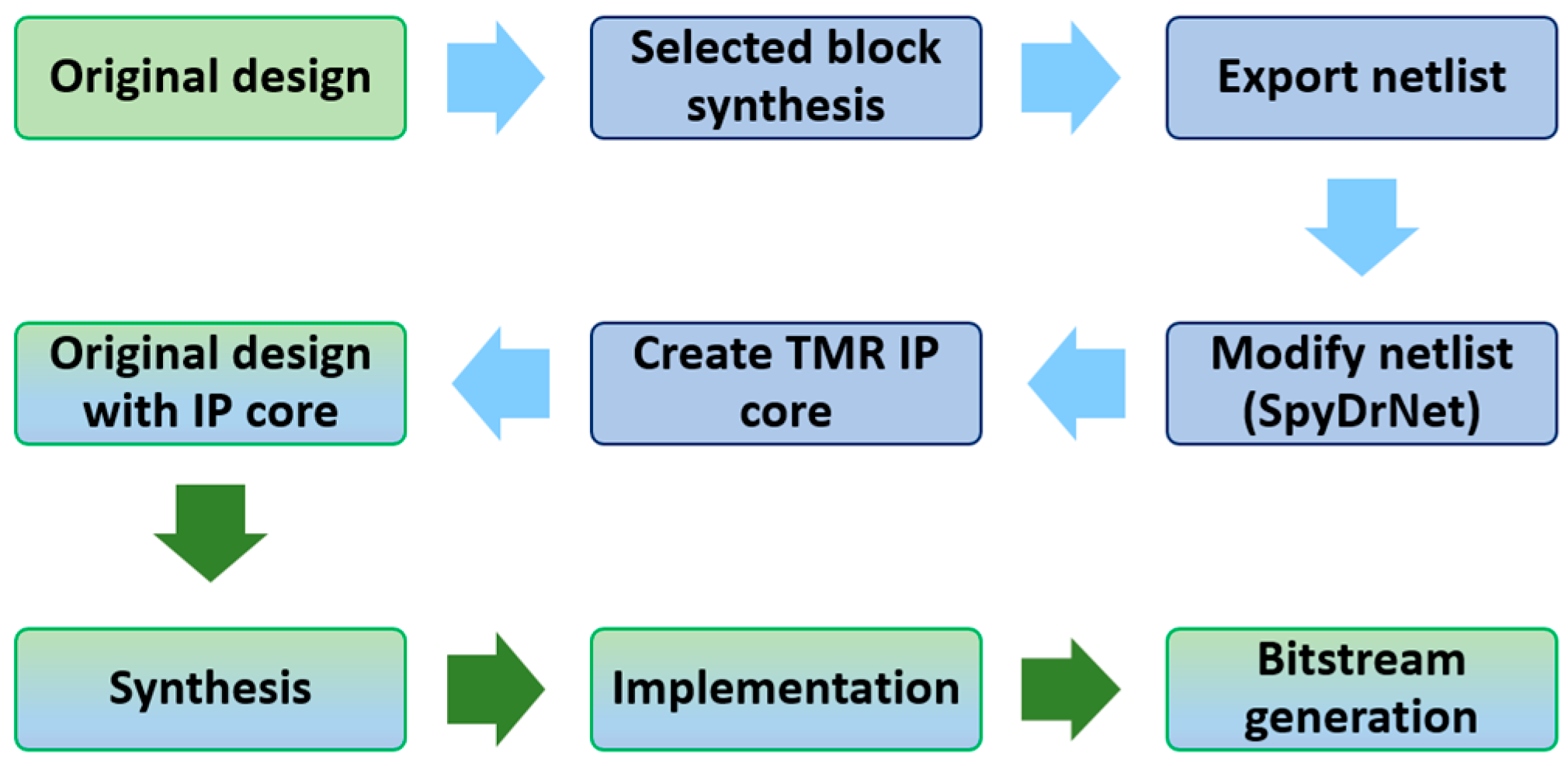
Figure 1. Design flow applied in this work, illustrating the transformation of the original implementation into a TMR-protected version.
Electronics 14 03318 g001
Figure 2. Vivado block diagram of the implemented design: the ecc_uart_0 block represents the kP accelerator with the UART interface, clk_wiz is a Clocking Wizard IP core configured to produce an output clock of 10 MHz.
Electronics 14 03318 g002
Figure 3. Design hierarchy of the kP accelerator, i.e., the ecc_uart_0 block on the block diagram in 0.
Electronics 14 03318 g003
Figure 4. Two instances of the same register i_z1: (a) original implementation in the Design_0, and (b) Triple Modular Redundancy (TMR) version in Design_2 and Design_3.
Electronics 14 03318 g004
Figure 5. Measurement position of the EM probe close to one of the power decoupling capacitors.
Electronics 14 03318 g005
Figure 6. A screenshot of the captured electromagnetic trace (red) for Design_0 and a trigger_out signal (green), indicating an ongoing kP operation. The duration of the kP operation is about 1.3 ms for the 10 MHz clock frequency.
Electronics 14 03318 g006
Figure 7. Representation of synchronized parts of the traces for all five investigated designs, consisting of 2000 samples, which corresponds to the duration of two clock cycles.
Electronics 14 03318 g007
Figure 8. Results of the conducted attack against the original design as well as its four instances employing triple modular redundancy.
Electronics 14 03318 g008
Table 1. FPGA resources utilization.
FPGA ResourcesAvailable Used
(Utilization)
Design Design_0Design_1Design_2Design_3Design_4
Slice13,3001775 (13.35%)3721 (27.98%)2302 (17.31%)4304 (32.36%)7542 (56.71%)
 SLICEL 13082664172030715094
 SLICEM 467105758212332448
LUT as Logic53,2005466 (10.27%)12,285 (23.09%)6790 (12.76%)13,687 (25.73%)22,705 (42.68%)
 Using O6 output only 46319723625911,12918,090
 Using O5 and O6 835256253125584615
Slice Registers106,4003706 (3.48%)5366 (5.04%)6502 (6.11%)8162 (7.67%)10,702 (10.06%)
 Register driven from within the Slice 18912727201428045274
 Register driven from outside the Slice 18152639448853585428
  LUT in front of the register is unused 11691045139413391775
  LUT in front of the register is used 6461594309440193653
Unique Control Sets13,30069 (0.52%)71 (0.53%)69 (0.52%)71 (0.53%)163 (1.23%)
Disclaimer/Publisher’s Note: The statements, opinions and data contained in all publications are solely those of the individual author(s) and contributor(s) and not of MDPI and/or the editor(s). MDPI and/or the editor(s) disclaim responsibility for any injury to people or property resulting from any ideas, methods, instructions or products referred to in the content.