Review

Electromigration Failures in Integrated Circuits: A Review of Physics-Based Models and Analytical Methods

1
College of Engineering, Peking University, Beijing 100871, China
2
School of Computer and Communication Engineering, University of Science and Technology Beijing, Beijing 100083, China
3
Peking University Nanchang Innovation Institute, Nanchang 330096, China
4
School of Rail Transportation, Soochow University, Suzhou 215131, China
*
Authors to whom correspondence should be addressed.
Electronics 2025, 14(15), 3151; https://doi.org/10.3390/electronics14153151
Submission received: 8 July 2025 / Revised: 28 July 2025 / Accepted: 4 August 2025 / Published: 7 August 2025
(This article belongs to the Section Electronic Materials, Devices and Applications)

Abstract

Electromigration (EM), current-driven atomic diffusion in interconnect metals, critically threatens integrated circuit (IC) reliability via void-induced open circuits and hillock-induced short circuits. This review examines EM’s physical mechanisms, influencing factors, and advanced models, synthesizing seven primary determinants: current density, temperature, material properties, microstructure, geometry, pulsed current, and mechanical stress. It dissects the coupled contributions of electron wind force (dominant EM driver), thermomigration (TM), and stress migration (SM). The review assesses four foundational modeling frameworks: Black’s model, Blech’s criterion, atomic flux divergence (AFD), and Korhonen’s theory. Despite advances in multi-physics simulation and statistical EM analysis, achieving predictive full-chip assessment remains computationally challenging. Emerging research prioritizes the following: (i) model order reduction methods and machine-learning solvers for verification of EM in billion-scale interconnect networks; and (ii) physics-informed routing optimization to inherently eliminate EM violations during physical design. Both are crucial for addressing reliability barriers in IC technologies and 3D heterogeneous integration.

1. Introduction

EM is a phenomenon where metal atoms in conductors move due to the transfer of momentum from flowing electrons [1,2]. EM causes metal atoms to move in the direction opposite to the electric field, leading to material diffusion and loss in metal conductors, which is a major reliability issue for electronic equipment [2]. While the fundamental mechanism involves momentum exchange, the practical consequence is the gradual displacement of metal ions, leading to material redistribution and potential failure in electronic components, particularly the miniaturized interconnect lines of integrated circuits (ICs) [3]. The dominant diffusion mechanism varies depending on the material and operating conditions; in bulk materials at elevated temperatures, lattice diffusion predominates, while in thin films, grain boundary diffusion becomes the primary pathway at lower temperatures and higher current densities [1]. Electromigration (EM)-induced failure modes primarily include the formation of voids (material depletion), hillocks (material accumulation), whiskers, and intermetallic phases under prolonged current stressing [4]. Void nucleation, growth, motion, and shape change all play crucial roles in the failure mechanism [3,5]. Predictive modeling of EM-induced void formation is critical for enhancing reliability in scaled ICs [6]. The spatiotemporal evolution characteristics—including void morphology development and positional migration—fundamentally determine interconnect failure rates, performance degradation, and nanostructure integrity in advanced metallization systems [7]. This void nucleation process predominantly results from hydrostatic stress gradients inducing localized mechanical degradation in conductor lines [8]. EM-induced void formation and growth in metal interconnects is a critical failure mechanism in microelectronics and can be influenced by a wide range of factors, including film purity, crystallographic orientation, grain size distribution, the presence of a passivating overcoat (e.g., glass), and the addition of solute atoms [1,9]. As IC dimensions continue to shrink and current densities increase, traditional mitigation strategies, such as simply increasing interconnect wire width, become impractical. This necessitates the development and implementation of innovative materials, design techniques, and process optimizations to effectively mitigate EM effects and ensure long-term reliability in advanced microelectronic devices [2].
EM poses a significant reliability threat to ICs, garnering considerable attention [10]. Alongside electrostatic discharge (ESD), EM remains a critical reliability concern as IC feature sizes shrink and packaging densities increase [11,12]. These trends, compounded by rising chip power and current densities, amplify EM’s impact, making it a primary concern in high-density IC packaging design. The now-discontinued International Technology Roadmap for Semiconductors (ITRS) consistently identified EM as a key limiting factor for such development [13,14], highlighting the enduring importance of understanding and mitigating this phenomenon. The increasing current densities within miniaturized solder joints and interconnects lead to increased EM-induced stress levels, creating significant long-term reliability challenges for advanced microelectronic devices [15]. With the development of advanced processes (5 nm and below) and 3D packaging technology, the effects of current density, temperature gradient, and material microstructure on EM are becoming more significant [16]. In particular, the extremely high current density and severe Joule heating in micro-bumps and solder joints make EM a major reliability concern in both three-dimensional ICs and conventional IC packaging [17,18,19]. Furthermore, EM in Ball Grid Array (BGA) packaging is a critical reliability issue determining product performance [20]. Persisting as a critical reliability bottleneck in technology scaling, EM imposes increasingly severe constraints on advanced IC design due to atomic-scale conductor geometries and heightened current densities [21].
As illustrated in Figure 1, the ITRS projected a continued increase in current density within IC interconnects, reaching magnitudes on the order of 106 A/cm2 [14]. According to the ITRS projections, EM-induced reliability concerns become significant when the current density approaches Jmax (region B in the figure). Furthermore, once the current density surpasses JEM (region C in the figure), the ITRS indicates that no existing process or design mitigations are sufficient to prevent EM-related failures. Compounding this challenge, the ITRS also warned that—even with a constant current density—the average lifetime of interconnects would be halved with each successive technology node generation due to ongoing reliability degradation caused by EM [14].
Beyond 2025, EM presents increasingly stringent reliability constraints due to aggressive interconnect scaling, rising current densities, and increasingly non-uniform thermal and mechanical stress conditions. Traditional EM current-density thresholds, historically treated as static design constraints, are becoming insufficient for predicting failure mechanisms in advanced nodes. The 2024 IRDS roadmap identifies EM as a persistent bottleneck, exacerbated by rising interconnect resistance driven by non-ideal barrier scaling and enhanced scattering at conductor interfaces and grain boundaries [22]. Recent studies emphasize that EM degradation is governed by multiple interacting physical effects. For instance, Rothe and Lienig (2023) demonstrated that under AC conditions, TM can dominate atomic transport, shifting peak tensile stress away from expected failure sites and significantly altering lifetime predictions [23]. These findings underscore the need to move beyond static threshold-based rules toward multi-physics EM models that incorporate self-healing, temperature gradients, and stress evolution, enabling more accurate and robust reliability analysis in future interconnect technologies.
This paper presents a comprehensive review of EM, covering fundamental principles, failure mechanisms, influencing factors, and related modeling and analysis methods. The remaining sections of this manuscript are organized as follows: Section 2 introduces the basic principles and physical phenomena underlying the EM effect. Section 3 categorizes the factors that influence EM-induced failure in ICs, analyzing the mechanisms by which each factor affects EM, as well as highlighting relevant research findings and engineering practices. Section 4 provides a detailed discussion of the material diffusion mechanisms associated with the three principal physical driving forces—electron wind, thermal gradients, and stress gradients—and further examines the interactions and coupling effects among these forces, emphasizing the challenges these tightly coupled phenomena pose for EM failure analysis. Section 5 delivers an in-depth analysis of classical and contemporary models for EM-induced failure. It begins with four widely used models: the Black empirical model, the Blech critical-product model, the atomic flux divergence (AFD) model, and the Korhonen stress-evolution model. The discussion covers their governing equations, physical interpretations, strengths, and limitations, as well as their applicable use cases in practical analysis. Furthermore, Section 5.5 introduces recent advances in EM modeling, including multiphase compact models, full-chip power grid reliability analysis techniques, electro-thermo-mechanical coupling frameworks, semi-analytical simulation accelerators, and physics-informed machine learning approaches such as PINNs and EM-GAN. These advancements reflect a paradigm shift toward multi-physics-aware and data-driven methodologies that enable scalable, high-fidelity EM reliability prediction for advanced technology nodes. Section 6 discusses current challenges and open questions encountered when applying EM failure analysis research in engineering practice. Section 7 concludes the paper by summarizing the key findings and proposing future research directions.

2. Fundamentals and Physical Phenomena of EM

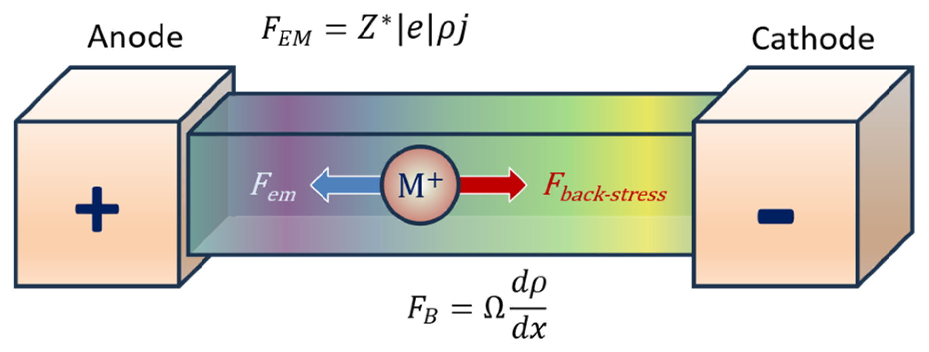
When an electric current is applied to a conductor, the metal ions within are subjected to two primary forces, as illustrated in Figure 2. The first is the electrostatic force ( F f i e l d ) also referred to as the direct force ( F d i r e c t ) in some literature, acting in the opposite direction to the electron flow. The second, the electron wind force ( F w i n d ), arises from momentum transfer during collisions between drifting electrons and the metal ions, acting in the same direction as electron flow. This phenomenon was first observed by Fiks in 1959 [24], who likened the force to a gentle breeze rustling leaves, thus coining the descriptive term “electron wind force”.
Due to the partial screening of the electric field by conduction electrons, the electrostatic force ( F f i e l d ) acting on positively charged metal ions is significantly weaker than the electron wind force ( F w i n d ). When the momentum transferred from drifting electrons surpasses the migration energy barrier (i.e., the activation energy E a ), metal ions are displaced from their lattice sites and migrate toward the anode. This directional flux of atoms results in material depletion at the cathode, forming voids, and material accumulation at the anode, forming hillocks. Such morphological changes can cause open-circuit failures at the cathode or short-circuit failures due to bridging at the anode, ultimately degrading the reliability of the interconnect system.
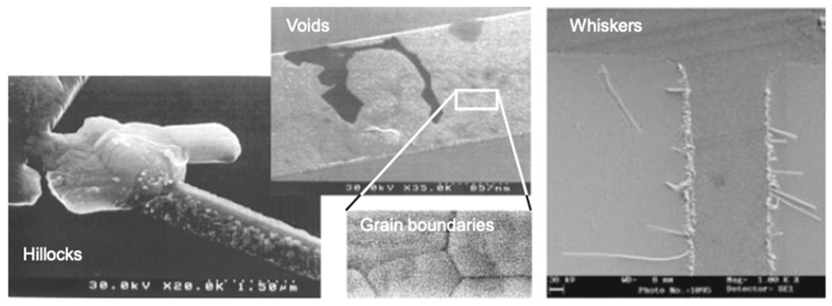
These phenomena have been directly observed using electron microscopy. Figure 3 presents representative SEM images of three EM-induced failure modes—void formation along grain boundaries, compressive hillock growth, and metallic whisker extrusion. These microstructural manifestations offer compelling evidence of EM-driven material transport under prolonged electrical stressing.
Beyond the typical hillock and void formation, EM can also induce secondary failure mechanisms such as whisker growth and grain boundary migration [25]. In particular, whisker formation—commonly observed in SnPb solder systems—involves the emergence of slender Pb/Sn filaments under sustained current stress [26]. Since grain boundaries act as fast-diffusion paths, localized geometric or thermal gradients can accelerate whisker extrusion, which poses a severe reliability hazard by enabling electrical bridging or arcing between adjacent interconnect lines.
While electron wind is recognized as the primary driving force behind EM failure, EM rarely occurs as an isolated phenomenon. Instead, failures in metal interconnect structures typically arise from the synergistic effects of multiple migration mechanisms, including electron wind, thermal gradients, stress gradients, and potentially chemical gradients. The interactions among thermal gradients, stress gradients, and electron wind will be examined in detail in Section 4. Although EM is a ubiquitous concern in electronic products, its impact on the reliability of ICs is disproportionately severe due to the extremely high current densities and ultra-fine interconnects characteristic of these devices. The following discussion classifies and analyzes the key factors affecting EM-induced failure in ICs.

3. Factors Influencing EM-Induced Failures in ICs

Since the initial observation of EM in metal interconnects by Fiks in 1959, extensive research has focused on understanding EM effects in ICs. These studies have revealed that EM is a multifactorial phenomenon influenced not only by current density and interconnect material but also by layout topology, interlayer dielectric composition, operating temperature, and signal frequency [27,28]. Interconnect layout—particularly via design—has a significant impact on current density distribution and EM reliability [25]. The microstructure at via-to-line transitions, with a strong emphasis on line properties, exhibits a clear correlation with observed failure modes [29]. As interconnect widths shrink to sub-micrometer dimensions, the influence of additional driving forces becomes more pronounced, necessitating the development of new modeling approaches [30]. In response to the growing challenges of EM in advanced technologies, researchers have explored innovative process integration schemes, such as copper (Cu)/cap interface engineering, alongside circuit design strategies that leverage specific layout characteristics [31]. The transition from aluminum (Al) to Cu interconnects has introduced new reliability challenges, primarily due to Cu’s higher diffusivity and poor adhesion to low-k dielectric materials [32]. Multiple via layouts can improve EM performance, with structures containing more vias showing better results [27]. These findings underscore the necessity of a co-optimization approach, encompassing interconnect process development, circuit design, and chip integration, to ensure EM reliability and optimize performance in future technology nodes [31]. The subsequent sections will systematically discuss these various factors and their underlying physical mechanisms that contribute to EM.

3.1. Current Density and Temperature

The current density in an interconnect is defined as the electric current flowing per unit cross-sectional area of the wire. Following the physical principle of EM, the electron wind exerts a force that propels the migration of metal atoms. Consequently, increasing the current density increases the frequency of collisions between electrons and metal atoms within the conductor, thereby accelerating the EM process. Furthermore, elevated temperatures enhance atomic diffusion, which can also exacerbate EM-induced failures. Thus, both current density and temperature are critical factors that directly influence the progression of EM-related degradation.
In 1961, Huntington and colleagues at Rensselaer Polytechnic Institute employed a surface scratch marking technique to investigate metal atom migration in metals such as silver, Cu, gold, and lead under high current densities. Their research demonstrated that the amount of migrated mass is directly proportional to both the current density through the conductor and the self-diffusion coefficient of the metal atoms [28,33,34,35]. Subsequently, in 1967, Black of Motorola experimentally derived a median time to failure (MTTF, i.e., operational lifetime) model for EM in Al interconnects, showing that the time to failure due to EM is inversely proportional to both the current density and the absolute temperature of the interconnect [36]. Extensive experimental and numerical analyses have since validated that, within a defined temperature range, current density remains a dominant factor influencing the EM lifetime of interconnects [37,38].
An increase in temperature supplies a portion of the activation energy needed for electron-driven atomic migration, thus facilitating the onset of EM. The atomic diffusion coefficient in metal interconnects exhibits an exponential relationship with temperature, as described by the Arrhenius equation [39]. This relationship is influenced by factors such as crystal structure, valence, and melting temperature [39]. Specifically, in Al interconnects, the thermal dependence of atomic flux is often modeled using a temperature-dependent activation energy, a parameter known to affect voiding behavior [40]. Consequently, elevated temperatures substantially accelerate ionic diffusion and migration processes. Cu interconnects are particularly susceptible to temperature variations; for instance, a 10 K increase in operating temperature necessitates a reduction of more than 50% in current to maintain the same MTTF. Conversely, a 5 K reduction in operating temperature allows for an approximate 25% increase in the permissible current density [41]. Furthermore, a temperature gradient also influences atomic migration processes, a phenomenon known as TM. The interplay between TM and EM will be discussed in detail in Section 4.
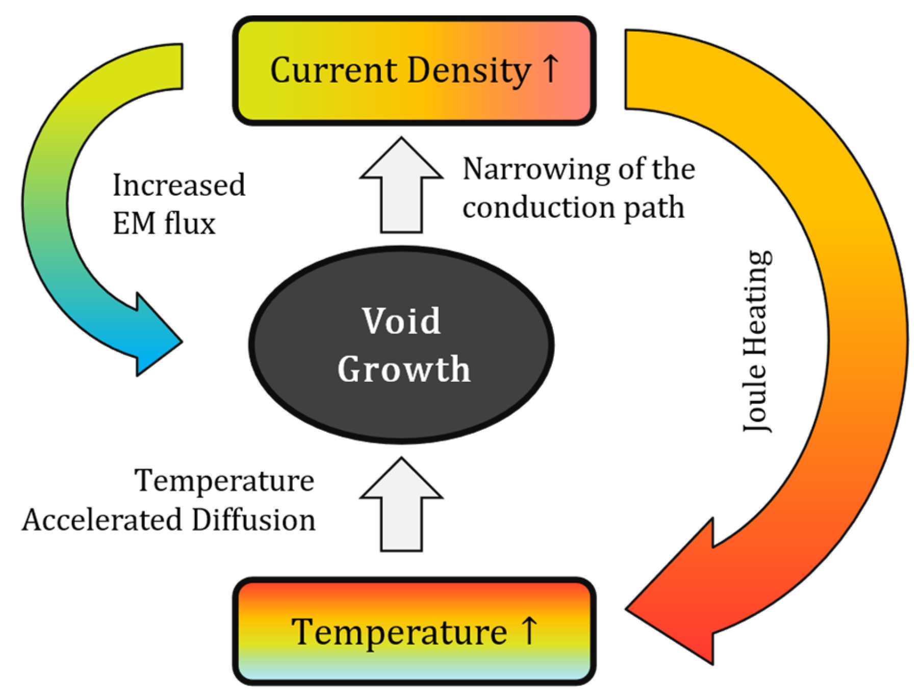
It is important to note that the interplay between current density and temperature can lead to a thermal positive feedback acceleration effect. Specifically, the passage of current through interconnects generates Joule heating, and the resulting temperature rise accelerates atomic diffusion within the EM process. This, in turn, promotes rapid void growth, reducing the conductor’s cross-sectional area. The reduction further increases the local current density, which generates additional Joule heating. As illustrated in Figure 4, this entire process forms a positive feedback loop: EM induces void formation → reduction in conductor cross-sectional area → increase in local current density → increased Joule heating → elevated temperature → accelerated EM-induced failure → further void growth [41]. This feedback loop significantly exacerbates EM degradation in ICs. Consequently, thermal coupling analysis—particularly simulations and analyses assessing the impact of self-heating on EM failure probability—has become a critical consideration in modern chip design [42].

3.2. Interconnect Materials

In the early development of ICs, Al was widely adopted as the metal interconnect material due to its low cost and ease of manufacturing. In 1970, Ames et al. at IBM discovered that incorporating a small percentage of Cu into pure Al could substantially improve the EM lifetime of Al interconnects [43]. Since then, the industry has routinely incorporated 2–3% Cu into Al interconnects to enhance their EM resistance. Extensive studies have sought to elucidate the mechanisms by which alloying elements inhibit EM [44,45,46,47]. Molecular dynamics simulations and energetic characterizations suggest that elements like Pd, Cu, Mn, and Sn may retard EM by increasing the activation energy for Al self-diffusion [48]. This effect is attributed to either a dragging effect in coupled substitutional–vacancy defects or an energy penalty for defect separation. Given Al primarily diffuses along grain boundaries, Cu enrichment at these boundaries may compensate for vacancies created by Al diffusion or increase the activation energy required for Al atom diffusion [49].
Due to the EM susceptibility, relatively high electrical resistance, and significant RC delay associated with Al interconnects, continuous scaling and increasing operating frequencies gradually made the RC delay of Al interconnects greater than the intrinsic delay of logic gates [50]. This created a bottleneck hindering IC development. Cu, possessing lower electrical resistivity and higher EM activation energy, became inherently more resistant to EM than Al [51]. Cu interconnects can withstand approximately five times the current density of Al interconnects under identical EM lifetime constraints [52]. Consequently, Cu replaced Al in ICs by the late 1990s, supported by the damascene process.
Despite Cu’s benefits, ongoing scaling has exposed limitations, particularly regarding EM reliability and resistivity at sub-5 nm nodes. Consequently, alternative materials such as cobalt (Co), ruthenium (Ru), and graphene-based structures have garnered significant attention. Initially, cobalt interconnects were considered but dismissed due to yield and cost issues. Nevertheless, recent advancements and ongoing research efforts have revisited their potential due to substantial EM reliability advantages. Cobalt (Co), owing to its higher melting point (1495 °C), significantly lower effective valence–diffusivity product relative to Cu, and favorable adhesion characteristics, has reemerged as a robust candidate for replacing Cu in narrow linewidth interconnects. Studies demonstrate that ultra-dilute alloying with MnO and W—at concentrations as low as 0.1% and 0.06%, respectively—can significantly enhance Co’s EM lifetime without introducing prohibitive resistivity penalties, by stabilizing grain structures and impeding void nucleation pathways through interfacial segregation mechanisms [53,54]. Furthermore, ruthenium offers compelling advantages including a short electron mean free path (<7 nm), compatibility with barrier-less integration, and high-temperature resilience. UV laser annealing (UV-LA) has significantly enlarged Ru grains, enhancing its EM performance while reducing resistivity to near-bulk values [55].
Another approach to enhancing the EM lifetime of metal interconnects involves the incorporation of a diffusion barrier layer surrounding the conductor. These layers typically comprise high-melting-point refractory materials, such as tantalum, titanium, or tungsten compounds, which offer significantly higher resistance to EM degradation compared to Cu and Al. As a result, when EM-induced voids nucleate within the Al or Cu lines, residual current can still flow through the surrounding barrier layer, thereby extending the overall effective EM lifetime of the interconnect structure [56,57]. However, it is important to note that the presence of the diffusion barrier layer can make the vias between different layers of the IC more susceptible to EM-induced void formation—a phenomenon that will be discussed further in Section 3.5.
Complementary to conventional metallic barriers, hexagonal boron nitride (h-BN) has recently emerged as an ultrathin dielectric diffusion barrier, particularly in ruthenium (Ru)-based interconnects. Owing to its chemical inertness and high thermal stability, h-BN enables Ru films to endure front-end-of-line (FEOL) thermal budgets, thereby reinforcing Ru’s suitability in advanced applications such as backside power delivery networks (BSDPNs) [58].
In the realm of carbon-based materials, graphene has demonstrated remarkable promise as both a protective capping layer and an active structural enhancement for EM reliability. When applied atop Co or Cu interconnects, graphene can improve the EM lifetime by factors of 4.5× and 78×, respectively, while simultaneously reducing line resistance and enhancing breakdown current density [59,60]. Moreover, graphene’s unique two-dimensional electronic structure allows for the modulation of EM-driving forces via electrostatic gating in resonant adsorbate systems, offering new mechanisms for nanoscale EM control [61].
To comprehensively compare these materials, Table 1 summarizes the relative EM performance, benefits, and limitations of traditional and emerging interconnects:
Collectively, these findings highlight that Co-, Ru-, and graphene-based systems offer distinct advantages for future interconnect schemes. Although integration challenges remain, their superior EM lifetimes and thermal stability position them as promising solutions to meet the stringent reliability demands of advanced sub-5 nm and 3D IC technologies. As integration strategies mature, these emerging materials are poised to surpass traditional Cu and Al interconnect performance benchmarks.

3.3. Microstructure

Metal atom diffusion—a critical aspect of EM—primarily occurs through three mechanisms, as illustrated in Figure 5: bulk diffusion (through the crystal lattice), grain-boundary diffusion (along grain boundaries), and surface diffusion (along the metal surface) [25,51,52]. The relative importance of each mechanism depends on factors such as temperature, material properties, and the microstructure of the interconnect.
Microstructural features determine which atomic transport pathway dominates EM. In polycrystalline, capped lines, diffusion proceeds preferentially along grain boundaries (GBs) and metal/dielectric interfaces, whose activation energies E a are markedly lower than those for bulk lattice diffusion. Table 2 compiles representative self-diffusion E a values for Al, Cu, Co, and Ru used in EM modeling, distinguishing bulk, GB, and surface/interface contributions.
For Cu, the high bulk barrier (~2.2 eV) renders bulk diffusion negligible in typical stress windows, leaving GB and surface/interface paths dominant. Co benefits from a slightly higher interface-controlled E a (~1.0 eV) and a GB E a around 1.1~1.3 eV, which—together with favorable adhesion/liner interactions—supports improved EM robustness at advanced nodes (albeit with higher resistivity than Cu). Ru couples an interface-controlled E a 1.0   e V with an EM-effective GB E a 1.8 eV, and exhibits a reduced resistivity size effect at narrow pitches, offering attractive EM–performance trade-offs for scaled wiring [25,68,70,73,74,77]. The hierarchy E a b u l k E a G B , E a s u r f a c e explains why EM voiding generally nucleates and grows along GBs and interfaces in capped interconnects. These values indicate that EM damage typically initiates at GBs and interfaces rather than through bulk diffusion—especially in Cu, where the bulk barrier is high.
Based on these activation energy hierarchies, EM tends to occur preferentially along interconnected grain boundaries and metal surfaces. The process of atomic migration at grain boundaries, ultimately leading to void formation, is well described by the triple junction model [56]. As illustrated in Figure 6, a triple junction is typically located at the intersection of three grain boundaries. Driven by the electron wind, if metal atoms flow into the junction through one grain boundary but flow out through the other two, a net outflow results. This leads to mass depletion and the formation of a void at the junction. Conversely, if atoms flow into the junction from two grain boundaries and out through the third, mass accumulation occurs, resulting in the formation of a hillock.
Therefore, reducing the number of triple junctions in interconnects is an effective strategy for improving EM lifetime [34,78,79,80]. For instance, as process technology scales down the wire width, when the width approaches the size of a single grain, most interconnected grain boundaries are truncated and eliminated, leading to the effective elimination of triple junctions. Consequently, the EM resistance of the interconnect can be significantly enhanced. The resulting metal microstructure, resembling a bamboo stalk lacking triple grain boundary intersections, is referred to as a “bamboo structure,” as illustrated in Figure 7.
Figure 7 further illustrates the variation in EM MTTF as a function of interconnect wire width. As shown on the right side of the curve, wire width has a direct impact on current density: wider interconnects exhibit reduced current density, which in turn enhances EM resistance. However, simply increasing wire width is not universally advantageous. Once the wire width falls below a critical threshold (denoted as w M T T F m i n the figure), a sharp increase in MTTF is observed. This counterintuitive improvement results from the formation of bamboo-like interconnects, which occur when the wire width becomes smaller than the average grain size. In such cases, the wire cross-section typically accommodates only a single grain, eliminating triple junctions and aligning grain boundaries perpendicular to the direction of electron flow. This orientation substantially restricts grain-boundary diffusion, thereby improving EM reliability. Nonetheless, the narrow width required to maintain a true bamboo structure is often impractical for high-current signal lines or power delivery networks, particularly in analog and mixed-signal circuits. To address this limitation, a slotted line technique may be employed. This involves patterning rectangular slots into the metal line to divide it into narrow segments, each adhering to the allowable width for a bamboo structure, while the overall metal width still satisfies the required current-carrying capacity. Alternatively, a fine-grained power mesh can be utilized, where multiple narrow metal lines—each conforming to bamboo structure constraints—are laid out in parallel to collectively conduct the required current [52].
Atomic surface diffusion is significantly influenced by the crystal plane orientation and crystallographic direction of the grains, as well as external environmental factors such as temperature, humidity, pressure, and contact materials, leading to complex behavior. Research indicates that high-symmetry crystal planes and dense crystallographic directions can reduce the reactivity of metal atoms, increase activation energy, and thereby suppress surface diffusion [81]. Interconnects tend to form a surface layer of Al oxide, which elevates the surface diffusion activation energy above that of grain-boundary diffusion. As a result, grain-boundary diffusion becomes the dominant atomic transport pathway in Al interconnects. Conversely, Cu exhibits a considerably lower surface diffusion activation energy compared to grain-boundary diffusion, making surface diffusion the primary transport mechanism. Given surface diffusion’s dominant role in Cu, EM in Cu interconnects most readily occurs at locations where the metal is in contact with other dielectric layers. In practice, EM resistance is improved through alloying, the addition of metal barrier layers, and surface treatment techniques [82].
In single-crystal interconnects, the absence of grain boundaries and triple junctions means that EM occurs predominantly through bulk diffusion. Under equivalent current and temperature conditions, single-crystal interconnects demonstrate significantly longer EM lifetimes compared to polycrystalline interconnects [83]. However, the fabrication of single-crystal interconnects poses substantial technical and economic challenges, and lattice defects within the single crystal can severely compromise process stability. Consequently, single-crystal interconnects have not seen widespread adoption in the semiconductor industry.

3.4. Geometric Shape

Given that current density is defined as the electric current per unit cross-sectional area of a conductor, and that the interconnect thickness is typically fixed in most fabrication processes, wider interconnects inherently have larger cross-sectional areas, resulting in lower current densities and thus longer EM lifetimes. However, experimental studies by Vaidya and Kinsbron have demonstrated that when the line width is reduced to approximately the same size as, or smaller than, the average grain size, the EM resistance can, paradoxically, improve despite the increased current density [78,79]. This enhancement is attributed to a significant reduction in the number of grain boundaries and triple junctions within the interconnect structure (as discussed in Section 3.3). EM resistance in metal interconnects exhibits a complex relationship with line width. For long Cu lines, EM failure time increases with wider lines due to higher critical current density. However, in short Cu lines, the opposite trend is observed [84]. For very narrow Cu wires (50–280 nm), EM resistance decreases significantly with decreasing width, and activation energy increases with the ratio of line length to average grain size [85]. EM in dual damascene Cu interconnects is affected by line width, with different dominant diffusion paths and activation energies below and above 1 μm width [86].
The length of interconnect lines also affects EM lifetime. In 1976, Blech and colleagues experimentally discovered that EM ceases when the wire length is reduced below a certain critical value. Blech proposed that voids and hillocks, formed by metal ion migration, generate a stress gradient within the conductor [87]. This stress gradient gives rise to a back stress—a mechanical force opposing the electron wind. This back stress drives metal ions in the opposite direction, reducing or even negating the net mass transport toward the anode, effectively suppressing EM. This phenomenon is known as the Blech effect, and the associated critical length is referred to as the Blech length or EM threshold length. Specifically, if the product of the interconnect current density J and line length l is less than a process-dependent threshold value J × l t h r e s h o l d , then the influence of EM on the interconnect can be considered negligible.
The bending angle of interconnect lines also influences EM lifetime. Electric current tends to follow the path of least resistance; therefore, the current density near the inner corners of interconnect bends is typically higher than in other regions. Consequently, careful attention must be paid to the geometry of interconnect bends, particularly avoiding sharp 90-degree corners, where the current density is substantially higher than with other bend angles [52].
The geometric structure at interconnect junctions also affects EM lifetime. Vias—electrical connections between different metal layers in an IC—are particularly vulnerable to EM-induced failure. To mitigate this, redundant vias are commonly employed to compensate for material depletion caused by EM [88]. However, if the current distribution across the via array is non-uniform, certain vias may experience disproportionately high current densities, accelerating localized damage. Therefore, careful design of redundant via layouts is essential to balance the current flow through each via and improve overall reliability.
In addition, a reservoir structure can be employed to enhance the EM resistance of vias. This technique involves extending the length of the metal line connected to the via, thereby creating a material reservoir that buffers against atom depletion caused by the electron wind. By increasing the available supply of metal atoms near the via, the onset of void formation can be delayed, effectively improving EM robustness [89].

3.5. Cu Interconnect Process

Due to their excellent electrical properties and relatively low cost, Cu interconnects have become the mainstream choice in modern ICs. Cu metallization—the process of forming interconnect structures by depositing Cu onto a wafer—is primarily carried out using the damascene technique. This technique involves a sequence of patterning and deposition steps typically described as follows: 1. Trenches or vias are first formed in the dielectric material using photolithography; 2. a diffusion barrier layer is deposited; 3. Cu metal is deposited on top of the diffusion barrier; 4. excess Cu outside the trenches and vias is removed using chemical mechanical polishing (CMP); and 5. a capping or passivation layer is deposited to complete the process.
Due to its low surface diffusion activation energy, Cu can readily diffuse into surrounding materials—particularly into interlayer dielectrics and, if unprotected, even into the silicon substrate—introducing impurities that degrade the electrical and semiconductor properties of the device [90]. Therefore, the diffusion barrier layer must provide both electrical conductivity and effective suppression of Cu diffusion into adjacent regions. After Cu deposition, an insulating cap layer such as silicon carbon nitride (SiCN) is deposited to passivate the surface, while tantalum-based materials are commonly used for the underlying diffusion barrier.
In Cu interconnect structures fabricated using the damascene process, metal lines within the same layer are typically arranged in parallel, while those in adjacent layers are often oriented perpendicularly. Vertical vias are used to establish interlayer connections and conduct current. The presence of diffusion barrier layers prevents cross-layer atomic transport at via locations; however, this also inhibits the replenishment of atoms migrating away from these regions. As a result, vias act as flux divergence points, making them locations where EM-induced voids commonly form. This phenomenon is illustrated in Figure 8.
Line Depletion: When electrons flow from a vertical via into a metal line on another layer, the EM effect causes Cu atoms to diffuse in the direction of electron flow. However, the diffusion barrier layer prevents Cu atoms at the via from diffusing into the lower interconnect, inhibiting atomic replenishment at the via-to-line junction. As diffusion progresses, a void eventually forms at this location, leading to increased line resistance and, potentially, an open-circuit failure.
Via Depletion: Conversely, when electrons flow from a horizontal line into a vertical via and then to another layer, the EM effect—combined with the presence of the diffusion barrier—inhibits the replenishment of Cu atoms lost from the via. This results in the formation of a void within the via (commonly referred to as via voiding), which can ultimately sever the electrical connection between the two metal layers. It is important to note that, because interconnect lines typically have a larger width than vias, under the same line current density, the via carries more total current and is therefore more susceptible to EM-induced damage.
Given that most current EDA tools assess EM reliability based on line current density, neglecting the width difference between interconnects and vias can lead to significant discrepancies between estimated and actual EM budgets, potentially impacting overall chip yield.

3.6. EM in Solder Joints

EM in solder joints presents a distinct set of challenges compared to EM in traditional Cu or Al interconnects. While metal interconnects typically experience EM failure at very high current densities (on the order of 106–107 A/cm2), solder joints—comprising Sn-based alloys with relatively low melting points and high atomic diffusivity—are susceptible to EM degradation at significantly lower current densities, usually between 104 and 105 A/cm2 [91,92].
The mechanisms of EM differ substantially between these two domains. In interconnects, atomic migration primarily proceeds along grain boundaries (for Al) or surfaces (for Cu), and the resultant damage usually takes the form of void formation or hillock growth along the conductor, eventually causing open or short circuits. These phenomena are well described by Black’s empirical model and Blech’s back-stress criterion. In contrast, solder joints are complex, multiphase systems containing coarse β-Sn grains, heterogeneous intermetallic compound (IMC) layers, and evolving microstructural boundaries. These features introduce multiple active diffusion pathways, including bulk diffusion through Sn grains, grain-boundary diffusion, and interfacial diffusion across solder/IMC and IMC/Cu boundaries [93]. Furthermore, synchrotron-based microdiffraction studies have revealed grain rotation in β-Sn under EM, even without grain growth. Unlike Cu and Al, where EM-related plasticity arises from dislocation movement, Sn grains rotate rigidly in response to uniaxial stresses generated by current crowding. This unique behavior further differentiates solder joint EM physics from those in crystalline interconnects [94].
Another distinct characteristic of solder joint EM behavior is three-dimensional current spreading, which creates non-uniform distributions of current density and temperature. This differs significantly from the uniform current paths in interconnect lines and can accelerate localized voiding, crack propagation, and phase segregation—particularly in low-melting solders like Sn–Bi systems. Moreover, solder joints often experience concurrent creep deformation and grain coarsening during service, leading to thermo-mechanical–electrical coupling in failure evolution [12]. To mitigate such effects, several strategies have been explored. One approach is to optimize diffusion barrier layers at the solder/Cu interface. Liu et al. showed that Co–W and Co–Fe–W alloy barriers outperform traditional Ni layers in suppressing IMC overgrowth. The Co–36Fe–17W barrier in particular promoted the formation of uniform CoSn3/FeSn2, thus impeding directional Cu diffusion and reducing EM-induced degradation [95].
A key factor influencing EM behavior in solder joints is the pronounced anisotropy of atomic diffusion in β-Sn, which adopts a body-centered tetragonal (BCT) lattice structure. This structure facilitates rapid atomic transport along the c-axis, making grains oriented in the ⟨001⟩ direction especially susceptible to accelerated Cu diffusion and intermetallic compound (IMC) formation under current stress. This anisotropic mass transport is further exacerbated by the presence of complex IMCs such as Cu6Sn5 and Cu3Sn, which serve not only as high-diffusivity pathways but also as preferential sites for crack initiation and mechanical degradation [96]. Yao et al. (2024) demonstrated that when the c-axis of Sn grains aligns closely with the direction of electron flow, Cu atoms migrate more efficiently, resulting in faster IMC growth and earlier EM-induced failure, even in the absence of geometric current crowding [19]. Similarly, experimental studies on Sn2.5Ag0.7Cu0.1RE solder joints revealed that the α-angle between the Sn c-axis and the current direction significantly affects fracture behavior and IMC morphology, reinforcing the critical role of grain orientation in determining EM reliability [97]. To address this, Lin et al. (2025) developed a (100)-textured Cu seed layer that induces favorable Sn grain orientations during solder reflow [98]. Their results showed that this engineered grain structure not only suppresses tin whisker growth but also reduces directional diffusion pathways for Cu atoms, enhancing both mechanical and EM stability [98].
The typical failure modes in solder joints also differ from those in metal lines. In planar interconnects, EM failure occurs within the conductor body, often at via interfaces or in current bottlenecks. In contrast, solder joints usually fail at the cathode side due to void formation along the solder/UBM (Under Bump Metallization) interface or within IMC layers. This is especially evident in flip-chip and micro-bump structures, where current crowding at UBM corners or CPB edges amplifies atomic flux divergence. As shown in Figure 9, voids can nucleate and coalesce along the Cu6Sn5/Sn interface on the cathode side, while the anode region exhibits thickened IMC layers without significant damage. Experimental observations by Chang et al. [99] demonstrated that EM-induced discrete voids at the IMC/solder interface on the cathode side can merge into interfacial cracks, ultimately resulting in UBM delamination, in contrast to the bulk erosion typically seen in metal interconnects.
The observed cathodic void nucleation in solder joints is in agreement with predictions from the AFD model, which describes net material depletion in regions of high current density. While stress-based models such as Korhonen’s framework have been successfully applied to predict stress evolution in interconnects, their applicability to solder joints is limited due to the joints’ multiphase composition and complex deformation behavior. In solder systems, interfacial characteristics and microstructural factors—such as β-Sn grain orientation and intermetallic compound (IMC) evolution—exert a dominant influence on EM reliability.
Thermal gradients further exacerbate these issues. In dense 3D packaging, Joule heating from high current densities often results in strong vertical and lateral temperature gradients, triggering TM in parallel with EM. This thermal–electrical synergy promotes mass transport toward the anode and accelerates void formation at the cathode. Studies have shown that such coupled degradation is more pronounced in solder joints than in interconnects due to the lower thermal conductivity and larger thermal expansivity of Sn-based alloys [93]. The issue of thermal coupling in 3D packaging will be further elaborated in Section 4.2.
Modeling EM in solder joints requires different approaches than those used for interconnects. Multiphase-field simulations of Cu/Sn/Cu joints reveal that vacancy evolution, IMC growth, and failure onset differ based on interface polarity. When the IMC/solder interface acts as the cathode, void nucleation is more prevalent, leading to asymmetric interfacial degradation. These findings suggest that conventional interconnect-centric EM models cannot adequately predict solder joint behavior under real-world stress conditions [100].
The multifaceted nature of EM in solder joints—encompassing microstructural anisotropy, interfacial evolution, current crowding, and TM—necessitates the integration of microstructural engineering, interface optimization, and predictive modeling to ensure long-term reliability. As modern ICs continue to scale and adopt heterogeneous 3D integration schemes, EM in solder joints will remain a critical reliability bottleneck that demands design co-optimization at both the material and system levels.

3.7. Pulsed Current and Frequency

Under normal operating conditions in ICs, the electron wind force is the primary driving mechanism for EM. Consequently, if the current direction in a wire reverses, the direction of metal atom diffusion also reverses, enabling the backflowing atoms to partially compensate for previous EM damage. This phenomenon is referred to as the (AC) self-healing effect and can significantly extend the EM lifetime of interconnects in ICs. Even if the current does not fully reverse, the cutoff periods inherent in pulsed current suppress or halt EM. Therefore, interconnects operating under unidirectional pulsed current conditions generally exhibit longer EM lifetimes than those under constant DC conditions.
The effectiveness of the self-healing effect in repairing EM-induced damage and the extent of damage incurred during unidirectional pulsed current operation are both dependent on the degree of lattice response during the peak current duration. This duration is determined by the pulse duty cycle and operating frequency. Therefore, under pulsed current conditions, both duty cycle and frequency are critical parameters that must be considered when calculating the EM time-to-failure of interconnects.
Experimental studies comparing resistance changes due to EM-induced voids under various frequencies have confirmed the significant impact of the self-healing effect on EM lifetime [101]. References [101,102,103] introduced a self-healing factor and proposed corrected models for MTTF that incorporate the effects of pulsed current frequency and self-healing dynamics. Tao et al. further found that, for Cu interconnects operating within the frequency range of 10 Hz to 104 Hz, the EM lifetime under high-frequency conditions can exceed that under low-frequency conditions by a factor of 500 [101,104].
As the driving frequency increases, the EM lifetime initially improves due to the self-healing effect, where alternating current periodically reverses atomic flux and mitigates net material transport. However, once the frequency exceeds approximately 104 Hz, the benefit of the self-healing effect begins to diminish. At these frequencies, EM in the forward and reverse directions approaches a quasi-equilibrium state, and TM gradually becomes the dominant degradation mechanism. When the frequency increases further—beyond 1010 Hz—the self-healing effect degrades rapidly. This degradation is attributed to the skin effect, where high-frequency alternating current (AC) concentrates current near the conductor surface, intensifying EM [105]. Combined with the fact that surface diffusion is the primary atomic transport path in Cu interconnects (as discussed in Section 3.3), this results in a renewed acceleration of EM and ultimately a reduction in interconnect lifetime at ultra-high frequencies.
It is important to note that neither the self-healing effect nor the high-frequency skin effect significantly impacts most modern digital circuits. Power lines in digital circuits typically carry direct current (DC), while most signal lines operate at megahertz or gigahertz frequencies, which are generally too high for effective self-healing, yet far below the threshold where the skin effect becomes significant. Nevertheless, studies on frequency dependence indicate that power lines are more susceptible to EM failure than signal lines. Therefore, when addressing EM reliability in digital IC design, it is essential to distinguish between power and signal interconnects and to balance reliability, cost, and performance appropriately.

3.8. Mechanical Stress

Mechanical stress gradients within the metal interconnects of ICs also influence EM lifetime. Tensile stress tends to promote void formation, while compressive stress—if exceeding a certain threshold—can cause material to extrude and diffuse into adjacent dielectric regions, forming dendrites, whiskers, or hillocks. These extrusions can cause damage similar to EM [25]. Mechanical stress in metal interconnects primarily arises from three sources.

3.8.1. Stress Gradients Induced by Thermal Expansion Mismatch

During fabrication, metal interconnects are deposited at elevated temperatures, often reaching 500 °C [106]. Upon cooling to ambient temperature, the mismatch in thermal expansion coefficients between the metal and the surrounding dielectric (e.g., SiO2) leads to non-uniform stress distributions. Specifically, tensile stress tends to build up in the center of the interconnect line, while compressive stress may occur near vias or line ends, creating a stress gradient along the interconnect structure. This stress gradient promotes void formation during the initial phase of EM in confined metal lines [107]. Kisselgof et al. investigated the impact of different deposition temperatures on EM performance, finding that lowering the processing temperature by approximately 15% (from 390 °C to 325 °C) significantly improved interconnect EM lifetime, by up to five times longer [108]. This improvement is attributed to the reduced tensile stress gradient within the interconnects after cooling, effectively enhancing their resistance to EM.

3.8.2. Stress Gradients Induced by Non-Uniform Metal Deposition Growth

During fabrication, non-uniform growth of metal layers during deposition introduces mechanical stress within the metal interconnects. This stress, characterizable through wafer curvature measurements [106,109], originates from intrinsic non-uniformities within the metal lines themselves. Studies have shown that its impact on EM lifetime can be even more severe than that caused by thermal expansion mismatch [106].

3.8.3. Stress Gradients Induced by Material Redistribution During EM

EM causes the redistribution of metal atoms and vacancies within interconnects, with atoms migrating toward the anode and vacancies accumulating near the cathode. Because vacancies occupy less volume in the crystal lattice than metal atoms, atom removal from the cathode region leads to lattice relaxation and volumetric contraction of the interconnect [110]. Conversely, atom accumulation at the anode causes volumetric expansion. Due to mechanical constraints from the surrounding dielectric material, this volume change is not fully accommodated, resulting in tensile stress at the cathode and compressive stress at the anode. Various studies have proposed methods for analyzing stress evolution in interconnects during EM [111,112,113,114]. In Section 4, we will further explore the interplay between stress gradients and electron wind forces and their combined effect on EM-induced failure.

4. Multi-Physics Driving Mechanisms of Atomic Migration

In the EM failure process, the electron wind force is not the sole driving mechanism; it often coexists with other migration phenomena such as TM, SM, and chemical migration [115,116]. Environmental or Joule heating from high current densities can induce a temperature gradient, driving metal atoms to diffuse from high-temperature to low-temperature regions. EM also causes material redistribution within metal lines, resulting in stress gradients (as discussed in Section 3.8). Combined with thermal expansion mismatches at elevated temperatures and residual stress from fabrication, these factors drive atom migration via stress-induced diffusion. Additionally, these migration processes lead to non-uniform atomic concentration distributions within the metal structure, forming concentration gradients that can induce further diffusion, a process known as chemical migration.
Therefore, EM in metal interconnects is, in fact, the result of the combined action of multiple migration mechanisms, making it a complex multi-physics problem. While chemical migration differs significantly from the other three mechanisms in its underlying physical processes, atomic concentration gradients have a relatively minor impact compared to other driving forces during the initial stages of EM failure [117], leading most current EM failure analyses to neglect their contribution. However, with the continued scaling of process nodes and feature sizes approaching the atomic scale, the influence of SM and TM on EM failure has become increasingly significant, making them critical reliability concerns in IC design. This section will further analyze the physical driving mechanisms and diffusion processes of EM, TM, and SM, and discuss their coupled interactions and impacts on the overall EM failure process.

4.1. Electron Migration (EM)

Although the term EM is now widely used to encompass combined migration effects—including EM, TM, and SM—its original meaning primarily referred to metal atom migration driven directly by the electron wind force and the electric field. Under current stress, conduction electrons in a metal move directionally and collide with metal atoms, exchanging momentum. Once a metal atom gains sufficient energy to overcome its energy barrier—the activation energy Ea—it escapes its equilibrium position and migrates to the next equilibrium site via grain-boundary diffusion, surface diffusion, or (less commonly) bulk diffusion. This momentum-exchange-driven atomic migration becomes particularly pronounced under high current densities and elevated temperatures. As a result, metal atoms migrate in the direction of electron flow (opposite to the direction of conventional current), from the cathode toward the anode, leaving behind vacancies at the cathode end.
As previously mentioned, Fiks termed the force generated by momentum exchange during electron–atom collisions the electron wind force, denoted as F w i n d , which acts in the direction of electron flow. In contrast, because metal atoms possess an effective positive charge, they also experience a Coulomb force parallel to the electric field, known as the direct force (or electric field force), denoted as F d i r e c t . This force acts opposite to the direction of electron flow, counteracting the wind force. The net force on migrating metal atoms is determined by the vector sum of these opposing forces.
The combined effect of the electron wind force and the direct electrostatic force is commonly referred to as the EM force, denoted as F E M [28]:
F E M = F d i r e c t + F w i n d  
To simplify the analysis, assuming complete momentum transfer during electron–atom collisions, the EM force can be expressed as follows:
F E M = F d i r e c t + F w i n d = Z d i r e c t + Z w i n d e E = Z e E
where Z d i r e c t * represents the ionic charge number (i.e., the valence of the metal atom), and Z w i n d * accounts for the momentum exchange effect. The total effective charge number Z * quantifies the net interaction between metal ions and conduction electrons. A smaller Z * indicates weaker momentum exchange between electrons and metal atoms. The value of Z * can be determined experimentally. e is the elementary charge, and E is the electric field strength, which is given by E = ρ j where ρ is the resistivity and j is the current density. Therefore, Equation (2) can also be written as follows:
F E M = Z e ρ j
The value of Z w i n d depends on the magnitude and direction of the momentum exchange between electrons and metal atoms, and can be calculated using the following formula:
Z w i n d * = n e ρ d m 0 n d ρ m * e E
where n e is the electron density, n d is the defect density, ρ d is the resistivity contribution from defects, m 0 is the free electron mass, and m * is the effective electron mass. The theoretical computation of Z w i n d * is relatively complex and has been explored using quantum mechanical approaches in [118,119,120,121]. Alternatively, it can also be determined experimentally. For metallic conductors, Z w i n d typically takes a negative value, indicating that its direction is opposite to that of the electric field. This reflects the fact that the momentum transfer from negatively charged electrons counteracts the electrostatic force acting on the positively charged metal atoms. Under high current density conditions, the magnitude of Z d i r e c t is much smaller than that of Z w i n d , meaning that the resultant EM force predominantly aligns with the direction of the electron wind.

4.2. Thermal Migration (TM)

TM is driven by temperature gradients. At elevated temperatures, the average velocity of atomic motion increases, resulting in a greater number of atoms diffusing from high-temperature to low-temperature regions than vice versa. This imbalance produces a net diffusion flux in the direction of the negative temperature gradient, potentially leading to significant mass transport (see Figure 10).
The primary sources of temperature gradients in metal interconnects are Joule heating caused by current flow and external thermal influences, such as localized self-heating from nearby high-performance transistors or external cooling mechanisms like through-silicon vias (TSVs) connected to heat sinks. Interestingly, TM contributes to the redistribution of heat, which reduces the thermal gradient and thus exhibits a self-regulating behavior. In contrast, electron migration lacks this capability. In EM, current density typically remains constant unless indirectly affected by circuit conditions such as a short circuit caused by EM reducing the supply voltage or an open circuit halting current flow. The driving force for TM is given by [122]:
F T M = Q * T T
where T is the absolute temperature, T is the temperature gradient, and Q * is the effective heat of transport. As IC areas continue to shrink while power densities increase, TM induced by temperature gradients has become a reliability concern that can no longer be ignored.
Schwarzenberger et al. experimentally observed that regions with the steepest temperature gradients often correspond to typical EM-induced failure sites [123]. Weiling et al., through EM experiments on Al-based metal lines, demonstrated that the direction of the temperature gradient significantly affects EM behavior: EM lifetime improves if the gradient increases in the same direction as electron flow, but is markedly reduced if the gradient opposes electron flow [124]. Nguyen et al. conducted similar experiments and provided quantitative data showing the impact of temperature gradients on EM lifetime [125]. Specifically, when the temperature gradient was 0.09 K/mm, 0.19 K/mm, and 0.28 K/mm, the interconnect’s EM lifetime was reduced to 90%, 40%, and 9% of the baseline (no gradient) value, respectively.
TM plays a particularly prominent role in metal alloys, such as solder materials. EM and TM, coupled with the Soret effect (differences in migration rates of alloy constituents), can lead to the dissolution of solder alloys [126,127]. High current density, for instance, causes rapid dissolution of the Cu cathode in molten Sn-based solder [127]. In practice, this issue is mitigated since most IC interconnects are composed of pure metals rather than alloys, making them less susceptible to these alloy-specific TM issues.
The advancement of advanced packaging technologies—particularly 3D stacking and TSV-based three-dimensional integration—has reduced overall chip size and significantly elevated power density, leading to more severe thermal issues. Furthermore, the heterogeneous nature of packaging structures can result in significantly larger temperature gradients in the package than within the chip itself. For example, a 10 K temperature difference across a 100 μm diameter flip-chip contact can create a temperature gradient as high as 1000 K/cm, sufficient to induce TM failures in solder materials [128]. Consequently, TM effects and simulation analysis within package solder joints have become a critical area of research.
In addition to package-level thermal challenges, vertically stacked three-dimensional integrated circuits (3D ICs) introduce additional complexities due to pronounced vertical thermal coupling. This phenomenon not only exacerbates TM but also intensifies EM degradation mechanisms. Unlike traditional planar structures, heat generated within lower dies must vertically propagate through upper dies, redistribution layers (RDLs), and micro-bumps, inducing spatially heterogeneous temperature gradients that amplify local thermal stresses and current crowding at inter-die interfaces, thereby exacerbating EM risks [129]. Experimental investigations by Choobineh et al. [130] and Matsumoto et al. [131] confirmed that significant inter-die thermal resistance can result in temperature differentials exceeding 10 °C under typical loading conditions, directly accelerating atomic migration driven by TM and significantly aggravating EM failures due to electro-thermal coupling. Additionally, finite-element analyses performed by Tian et al. [132] revealed that regions experiencing maximum overlap between vertical temperature gradients and high current densities (approximately 4.0–4.5 A/cm2) are particularly vulnerable to premature micro-bump EM failures. Similarly, Zhang et al. [133] developed an electro-thermal reliability model specifically for 3D TSV-RDL structures, further verifying that vertical thermal fluxes and non-uniform cooling pathways critically influence EM lifetime predictions by inducing localized overheating, decreasing mean time to failure (MTTF), and triggering early-stage atomic flux divergence. Consequently, contemporary design strategies have emphasized thermal-aware placement and routing algorithms that explicitly leverage vertical thermal coupling characteristics, optimizing inter-die heat transfer to effectively mitigate the combined degradation effects of EM and TM [134].
Thus, vertical thermal coupling in 3D ICs not only magnifies TM phenomena but also establishes a strong interaction with EM mechanisms, introducing additional complexity into EM-induced failure modes. In response to these emerging challenges, future reliability analyses and chip-design methodologies should further explore TM effects from an integrated multi-physics perspective. In the subsequent section, we will discuss the mechanism of SM and its intricate interactions with the previously discussed migration phenomena.

4.3. Stress Migration (SM)

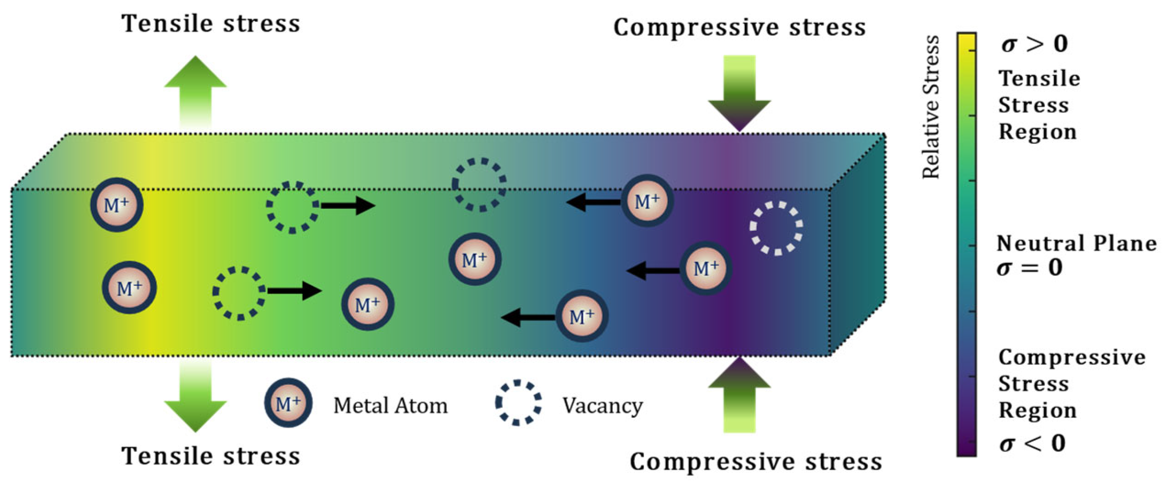
SM refers to atomic diffusion driven by stress gradients, a process that redistributes and rebalances mechanical stress within a material. When a stress gradient exists within a metal interconnect—regardless of its origin (internal or external)—tensile stress induces a net influx of atoms, while compressive stress causes a net outflow. Similar to TM, this results in metal atom diffusion along the negative direction of the mechanical stress gradient (see Figure 11).
The primary causes of mechanical stress in metal interconnects of ICs include the following (see Section 3.8): a mismatch in thermal expansion coefficients; non-uniform metal deposition during fabrication; and uneven material distribution caused by other migration mechanisms. Metallic crystal lattices typically contain unoccupied lattice sites, known as vacancies. Because vacancies occupy less space than atoms, a crystal with a higher concentration of vacancies will exhibit lattice volume relaxation, resulting in a smaller volume compared to a crystal with more fully occupied sites [110]. As a result, vacancies play a central role in the SM process.
According to Hooke’s law, the relationship between stress and volumetric strain in a metal can be expressed as σ = E · ε , where σ is the mechanical stress, E is the Young’s modulus, and ε is the volumetric strain induced by stress.
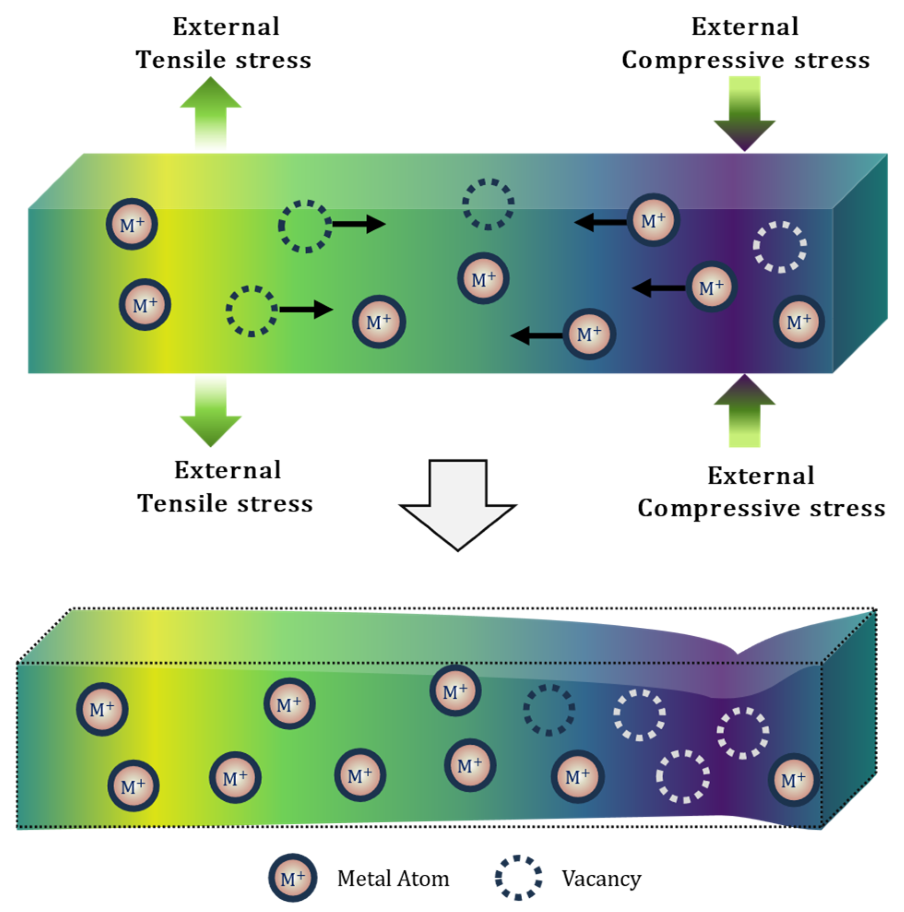
Mechanical stress comprises both tensile and compressive components. Stress gradients drive atoms from compressive to tensile stress regions, and simultaneously push vacancies in the opposite direction. Because tensile stress correlates with volume expansion and compressive stress with volume contraction, stress-induced diffusion acts to restore equilibrium within the stress field. For example, if an external mechanical force induces the stress gradient, atoms in the compressive region will be displaced outward. This outflow leaves behind vacancies and leads to lattice relaxation, reducing the metal volume within the compressive region. This volume reduction helps alleviate the external pressure until mechanical equilibrium is reached, as illustrated in Figure 12.
If the stress is internally generated by other migration processes—such as EM or TM—initially, vacancy-rich regions will experience internal tensile stress, while atom-rich regions will develop internal compressive stress. Under the resulting stress gradient, atoms diffuse from the compressive (atom-rich) regions toward the tensile (vacancy-rich) regions, compensating for the original migration process and eventually reaching a new equilibrium state. However, if the number of vacancies induced by external stress or EM exceeds a critical threshold, vacancy supersaturation may occur, leading to the coalescence of multiple vacancies into a void. This phenomenon, known as void nucleation, typically signifies the initiation of cracking in the metal line. The subsequent crack formation releases accumulated stress, allowing the system to reach a new mechanical equilibrium, as illustrated in Figure 13.
The driving force for SM is given as follows:
F S M = Ω σ ¯
where Ω represents the atomic volume, and σ ¯ is the hydrostatic stress, defined as σ ¯ = ( σ x x + σ y y + σ z z ) / 3 .
It has long been recognized that Joule heating from electrical current introduces thermal gradients, making TM a factor in EM-induced failure. However, the influence of SM on EM reliability was studied somewhat later. In 1976, Blech and colleagues at Bell Labs were the first to identify mechanical stress as a migration-driving mechanism as equally important as the EM force [87]. With the continued scaling of feature sizes and the advancement of heterogeneous packaging technologies, the effects of thermal expansion mismatch and residual stress introduced during fabrication have become increasingly significant contributors to EM failure. The following section will further analyze the interactions among TM, SM, and EM.

4.4. Coupling Effects in Multi-Physics Migration

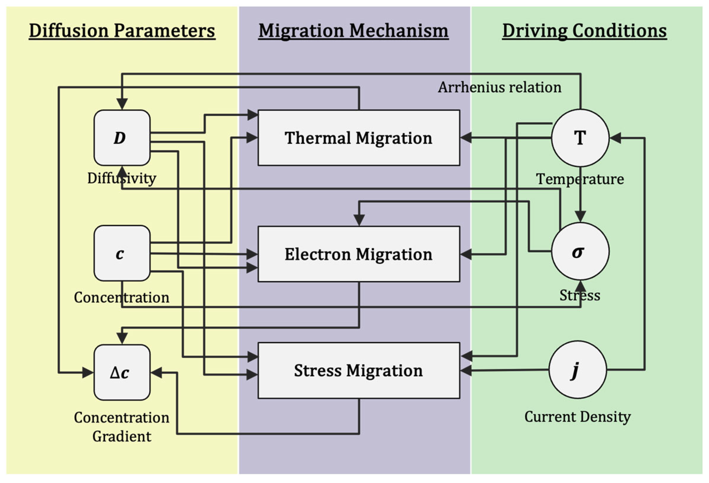
As discussed, EM in metal interconnect structures is, in fact, the result of multiple migration mechanisms acting simultaneously. It is a dynamic process where electrical, thermal, and mechanical driving forces interact and eventually reach equilibrium. Internally, current flow through interconnects generates Joule heating. Due to differences in thermal conductivity between the metal lines and surrounding dielectric materials, non-uniform temperature distributions arise within the interconnects. Under the resulting temperature gradient, metal atoms migrate along the negative temperature gradient towards decreasing temperature. Therefore, TM mitigates EM when the temperature gradient opposes electron flow; conversely, it exacerbates EM when the gradient aligns with electron flow.
Moreover, as EM and TM proceed, the redistribution of atoms and vacancies generates stress gradients. Under these gradients, atoms diffuse from compressive to tensile regions. Because this diffusion opposes the EM-induced atomic flux, SM can counterbalance EM, helping the system reach a new equilibrium. Externally, high-frequency transistors may generate substantial heat during operation, while heterogeneous structures in 3D packaging introduce more pronounced temperature gradients. These factors alter the temperature distribution along the interconnects and induce TM. Simultaneously, mismatches in the coefficients of thermal expansion among the substrate, dielectric layers, and surrounding materials can lead to uneven deformation at high temperatures. This results in externally applied compressive or tensile stress on the metal interconnects, creating stress gradients that drive SM.
When thermally or mechanically induced migration—triggered by these external factors—exceeds a certain threshold, voids can form. These voids reduce the cross-sectional area of the metal lines, increasing line resistance and altering the local current density, which in turn affects EM. Additionally, the resulting increase in Joule heating further modifies the temperature gradient, completing a feedback loop that reinforces the interplay between thermal, electrical, and mechanical effects. Variations in temperature and stress also influence key driving factors and parameters—such as electrical resistivity, atomic diffusion coefficients, and atomic concentrations—which in turn affect the diffusion behavior of all three types of migration. Consequently, not only do the atomic and vacancy diffusion processes of EM, TM, and SM interact, but their driving forces and governing parameters are also interdependent. This creates a complex and tightly coupled multi-physics system [25] (see Figure 14).
EM-induced failure results from the combined effects of the three interacting migration mechanisms described above. It is important to note that the dominant driving force varies depending on the specific scenario and phase of the failure process. For example, Tan et al. conducted coupled electro-thermal simulations on both Al and Cu interconnects [135]. Their findings revealed that, in Al interconnects, TM is not a significant factor, and atomic migration is primarily driven by the electron wind force. In contrast, for Cu interconnects, TM is the dominant driving force during the early stages of atomic migration, while the electron wind becomes the prevailing factor in the later stages.
The complex and tightly coupled multi-physics interactions within IC metal interconnects present significant challenges for simulating and analyzing EM-induced failure. The simultaneous operation of migration driven by electrical, thermal, and mechanical fields, combined with intricate boundary conditions and interdependent parameters, makes transient analysis of EM failures extremely complex and, at times, numerically non-convergent. Furthermore, the vast scale of modern advanced ICs, containing internal logic blocks with hundreds of millions of gates, leads to enormous and complex simulation models. The computational power and time required for high-accuracy numerical analysis often exceed practical engineering feasibility.
Over the past few decades, the engineering and scientific communities have proposed numerous mathematical and physical models to analyze EM failure. Several have become particularly classical and widely adopted, including empirical models based on experimental data (e.g., Black’s empirical equation and Blech’s critical current–length model), the AFD model based on mass conservation principles, and the relatively simplified Korhonen stress evolution model. The following section will introduce and derive the mathematical and physical formulations for each of these models.

5. EM Failure Analysis Models

5.1. Black’s Empirical Model

In 1967, building upon the earlier work of Huntington and Grone [28], Black proposed an empirically derived model for the MTTF of Al interconnects under EM stress [136,137]. This resulted in the well-known EM MTTF equation, commonly referred to as Black’s equation:
t M T T F = A J n e x p E a k B T
where t M T T F is the median time to failure, A is a constant related to material properties and the cross-sectional area of the conductor, J is the current density in the wire, n is a dimensionless empirical constant that depends on the conductor material and the failure criterion used, Ea is the activation energy for EM, and kB is Boltzmann’s constant.
We must revisit and re-derive Black’s equation to analyze its underlying physical meaning, particularly the physical quantities related to the constant A. Black proposed that EM-induced failure in a metal interconnect (modeled as a flat wire with width w and thickness t ) occurs when the total amount of material transported through the wire’s cross-sectional area exceeds the amount of material contained in that unit cross-section ( w × t ). At this point, the interconnect experiences an open-circuit failure due to complete material depletion. If R m denotes the EM-driven material flux rate (the amount of atomic material transported per unit area per unit time), then the median time to failure t M T T F can be expressed as follows:
t M T T F = F 1 w × t R m
where F 1 is an undetermined constant. Early theoretical studies on EM considered the electron wind force as the primary driving mechanism, where metal ions migrate due to momentum transfer from colliding electrons. Based on this, Black assumed that conduction electrons undergo nearly perfectly elastic collisions with metal atoms, transferring their full momentum to the atoms during each collision. Under this assumption, the material migration rate R m , which is defined as the number of atoms transported per unit area per second, is directly proportional to the following factors: the momentum of an electron P e , the number of electrons passing through a unit volume per second N e , the number of electrons passing through a unit volume per second N a , and the ionic scattering cross-section Σ , which represents the probability of collisions per unit time. Therefore, R m can be expressed as follows:
R m = F 2 × P e × N e × N a × Σ
where F 2 is a constant and the momentum gained by an electron as it travels through an electric field E with an average velocity v over its mean free path p f can be expressed as follows:
P e = e E p f v = e ρ j p f v  
where e is the elementary charge, and j is the current density. The number of electrons passing through a unit volume per second is related to current density and is given as follows:
N e = j e
The number of atoms thermally activated to overcome the energy barrier per unit volume, N a , is related to the atomic diffusivity D, which follows the Arrhenius law:
D = D 0 exp E a k B T
where D 0 is the pre-exponential diffusion constant, and E a is the activation energy for atomic migration. By combining Equation (9) through Equation (12), we obtain the following:
R m = F 2 D 0 × ρ p f j 2 v exp E a k B T
Substituting Equation (13) into Equation (8) and replacing the known constants ( D 0 ,     ρ , p f , v , w , t ) and the unknown factors ( F 1 , F 2 ) with a lumped constant A, we arrive at the expression for Black’s empirical model:
t M T T F = A j 2 exp E a k B T
This equation highlights that the constant A is related to numerous physical properties, including metal resistivity, electron mean free path, average electron drift velocity, ionic scattering cross-section, and the pre-exponential diffusion constant. Consequently, determining A requires extensive experimental calibration to account for variations in these parameters, classifying Black’s equation as an empirical model.
It is also worth noting that when Black originally proposed this empirical equation, the exponent on the current density term was fixed at two, rather than a general exponent n. This was closely related to the experimental conditions and the characteristics of the Al wire material used at the time. However, as the feature sizes of ICs have continued to shrink and new materials such as Cu interconnects have been adopted, increasing discrepancies have been observed between the predictions of Black’s model and actual wire lifetimes [138]. In 1971, Blair et al. [66] proposed a modification to the original Equation (14), replacing j2 with jn, resulting in the generalized form shown in Equation (7) [139]. They also pointed out that the value of n typically lies between one and two, and must be determined experimentally for each specific material and test condition.
In fact, the appropriate value of the exponent n has long been a subject of debate. Various experiments and studies have reported different values of n, depending on the current density range: For 10 5 A c m 2 < J < 10 6 A c m 2 , n = 1.5 [140]. For 5 × 10 5 A c m 2 < J < 2.8 × 10 6 A c m 2 , n = 2 [141]. For 10 6 A c m 2 < J < 2 × 10 6 A c m 2 , n = 4 5 [142]. Hau-Riege conducted an in-depth investigation into this issue and pointed out that the variation in n primarily arises from differing failure criteria [32]. Specifically, when n = 1, the time to failure is dominated by the growth phase of the void—i.e., the time it takes for a pre-existing void to grow large enough to cause failure. In contrast, when n = 2, the failure time is governed by the nucleation of the void itself.
Despite its pioneering role in establishing the quantitative relation between EM failure time, current density, and temperature, Black’s empirical model exhibits several notable limitations when applied to complex, real-world scenarios. Its parameters (n and Eₐ) are typically obtained via accelerated stress tests—often resembling protocols such as JEDEC JESD22-A104 [143] or IPC-9701 [144]—even though these tests typically impose thermal extremes ranging from −55 °C to +125 °C with rapid transition rates and short dwell durations (e.g., <10 min per dwell), or extended cycling between −40 °C and +125 °C over 1000+ cycles. By contrast, actual interconnects in the field often operate under steady-state temperatures in the 60–100 °C range, with thermal cycles occurring far less frequently (e.g., <100 cycles/year), and packaging-induced mechanical stress evolving gradually rather than abruptly. This disparity in stress profiles introduces significant variability in EM model calibration.
Black’s equation inherently assumes isothermal, steady-state current stressing. However, parameters n and Eₐ extracted under dynamic or non-equilibrium conditions may not faithfully reflect the diffusion mechanisms active in operational environments. For instance, Cui et al. demonstrated that void formation and current crowding behavior in solder joints under IPC-9701A-guided thermal cycling (125 °C, 1.4 A) cannot be captured by conventional Black modeling alone, with observed lifetime deviations exceeding 44% when compared to empirical tests [145]. Instead, AFD-based simulation yielded MTTF predictions within 10% of experimental values, highlighting the inadequacy of uncalibrated empirical models. Ruiz et al. further emphasized that uncontrolled test conditions—such as temperature overshoot, asymmetric dwell, or poorly regulated ramp rates—can propagate into parameter estimation uncertainty, undermining model fidelity [146].
Moreover, the model does not consider compensating SM effects, which can lead to overly conservative lifetime estimates [147]. It was originally formulated for isolated, linear interconnects and does not extend well to networks with directional changes, multi-layer routing, or packaging-induced non-uniformities [148]. Hybrid strategies—such as test-specific calibration using in situ current stressing under IPC-9701-based cycles, combined with FEM and electro-thermal simulation [149]—have emerged to improve parameter fidelity and extend predictive power to advanced packaging structures.
Nevertheless, when augmented with such calibration methods and modeling enhancements, Black’s model remains a fast, effective tool for preliminary EM lifetime estimation in engineering workflows. Its simplicity, efficiency, and enduring relevance justify its continued use alongside more complex models like the Blech critical-product model.

5.2. Blech Critical Model

In 1976, I. A. Blech and his colleagues at Bell Laboratories conducted EM experiments on thin Al films deposited on titanium nitride surfaces [87]. Their experiments revealed that when the interconnect length is shorter than a certain critical threshold—approximately 20 to 30 μm under the process conditions of that time—the effects of EM diminish and eventually disappear. This phenomenon is known as the Blech effect, and the corresponding threshold length is referred to as the Blech length (or EM critical length).
Blech attributed the existence of a critical length to the back-stress effect. He proposed that, under the driving force of EM, the distribution of metal atoms within the interconnect becomes non-uniform: voids form at the cathode, generating tensile stress, while metal atom accumulation at the anode produces compressive stress. This results in a stress gradient that drives metal atoms to flow back from the anode toward the cathode—a phenomenon referred to as back-stress flow or the backflow effect. As illustrated in Figure 15, Blech proposed that two forces influence the motion of metal atoms within a conductor [88]: (1) The EM driving force F E M , which is the combined effect of the electron wind force and the electric field force, points from the cathode to the anode and drives metal atoms to migrate toward the anode. (2) The back-stress force F B , which arises from the non-uniform distribution of atoms caused by EM, acts in the opposite direction—from the anode to the cathode—and drives atoms to flow back toward the cathode, effectively counteracting EM and contributing to self-healing.
According to Section 4.1 and Section 4.3, we know that the EM force is given by F E M = Z * e ρ j , and the back-stress force is given by F B = Ω d σ d x . Assuming that the back-stress is uniformly distributed and considering only the stress gradient along the direction of the interconnect line, we can approximate the stress gradient as follows:
F B = Ω d σ d x Ω σ x x l = Ω σ t h r σ 0 l
where l is the length of the metal interconnect, and σ x x denotes the difference in hydrostatic stress along the longitudinal direction of the interconnect—that is, the stress gradient between the anode and cathode ends, typically expressed as   σ t h r σ 0 . Blech proposed that when the EM driving force and the back-stress force reach equilibrium, the backflow effect induced by the stress gradient fully counteracts the effect of EM. This equilibrium is achieved when
Z e ρ j   Ω σ t h r σ 0 l
Rearranging the terms yields the critical product of current density and line length—also known as the Blech condition:
j l j l c = Ω σ t h r σ o e Z ρ
According to this equation, the critical length l c can be determined by measurement under a given current density. Similarly, for a given interconnect length, the maximum allowable current density j c can also be obtained. In addition, the model allows for the estimation of EM’s impact on wire resistance [150]. Therefore, the Blech critical model has been widely adopted in engineering practice. Interconnect length can be reduced during IC design to avoid EM violations. Additionally, because interconnect segments shorter than the Blech length theoretically do not experience EM-induced failure, they can be excluded from simulation analysis, which significantly reduces the computational complexity of EM simulations.
Blech was the first to recognize SM as an additional driving force opposing EM. It is worth noting that, with the continuous scaling of technology nodes, the sources and characteristics of back stress in microelectronic structures of ICs are increasingly affected by temperature and residual stress introduced during the manufacturing process. Therefore, empirical models must be continuously refined and updated in accordance with process evolution; otherwise, they may yield inaccurate Blech critical lengths and maximum allowable current densities, thereby compromising the accuracy of EM sign-off.

5.3. AFD Model

In 2001, Dalleau et al. introduced the AFD method for EM lifetime prediction, based on mass diffusion and conservation principles [151]. They proposed that EM-induced failure stems from atomic migration, which causes material diffusion and mass transport. When mass transport becomes unbalanced—meaning the amount of incoming atoms differs from that of outgoing atoms—voids or accumulations may form, ultimately leading to EM failure.
Generally, the quantity of diffusing atoms passing through a unit cross-sectional area perpendicular to the diffusion direction per unit time is referred to as the atomic diffusion flux. The variation of this atomic flux at a certain point is called atomic flux divergence. Therefore, regions with nonzero atomic flux divergence correspond to mass transport imbalances—precisely the locations where EM-induced failure is likely to occur. Letting the atomic flux be denoted as J , under steady-state diffusion conditions, atomic diffusion behavior can be described by Fick’s First Law, which can be written as follows:
J = D C
where D is the diffusion coefficient, which follows the Arrhenius law (see Equation (12)) for its expression, and C is the concentration gradient. The negative sign indicates that atomic diffusion occurs in the direction of decreasing concentration—that is, from regions of high concentration to low concentration. The physical meaning of this equation is that the amount of material diffusing through a unit area perpendicular to the diffusion direction per unit time is proportional to the local concentration gradient at that cross-section. In fact, most diffusion processes are non-steady state, where the concentration varies with time. Such transient diffusion processes can be described by Fick’s Second Law:
C t = J = [ D C ]
where t denotes time, and is the divergence operator. The physical meaning of Equation (19) is that the time rate of change in atomic concentration at a cross-section equals the divergence of the atomic flux—that is, the difference between the inflow and outflow of atoms per unit volume (flux divergence) corresponds to the local concentration variation. Under thermodynamic equilibrium conditions, the atomic concentration distribution follows the Boltzmann distribution, given as follows:
C x = C 0
where ϕ x is the potential energy function and C 0 is the initial concentration. Taking the derivative of both sides with respect to x , Equation (20) can be rewritten as follows:
d C d x = C 0 e x p ϕ ( x ) k B T 1 k B T d ϕ d x = C k B T d ϕ d x
According to the potential energy gradient interpretation, d ϕ d x can be interpreted as the force F c acting on atoms along the direction of the potential, where the negative sign indicates the force direction is along the negative gradient of potential energy—that is, from high to low potential. Therefore, the relationship between the concentration gradient and the potential force is as follows:
d C d x = C k B T F c
By substituting this expression into Fick’s First Law, the atomic flux can be reformulated as a function of the driving force acting on the atoms:
J = D C k B T d ϕ d x = C D k B T F
As discussed previously, EM-induced failure is the result of the combined effects of three driving forces: the EM driving force F E M , the TM driving force F T M , and the SM driving force F S M . Based on the aforementioned equations, the atomic diffusion flux models corresponding to these three driving forces can be expressed individually.
The atomic diffusion flux due to EM is given as follows:
J E M = C D k B T F E M = C k B T D e Z E = C k B T D 0 exp E a k B T e Z ρ j
The atomic diffusion flux due to TM is given as follows:
J T M = C D k B T F T M = C Q k B T 2 D T =   C Q k B T 2 D 0 exp E a k B T T
The atomic diffusion flux due to SM is given as follows:
J S M = C D k B T F S M = C Ω k B T 2 D σ ¯ = C Ω k B T 2 D 0 exp E a k B T σ ¯
The total atomic diffusion flux J is the sum of the fluxes driven by EM, TM, and SM. Therefore, the total flux divergence is given by the following:
d i v J = d i v ( J E M + J T M + J S M )
To facilitate analytical modeling, the total divergence can be expressed as a function of relevant physical parameters:
d i v J = C F E a ,   D 0 ,   k B ,   σ ¯ ,   Ω ,   = C F
According to the principle of mass conservation, the divergence of atomic flux within a region equals the rate of change of atomic concentration in that region:
d i v J + C t = 0
Thus,
C F + C t = 0
By applying an explicit Euler integration scheme, the evolution of atomic concentration over time can be modeled as follows:
C i + 1 = C i e F i t i t i = ln C i C i + 1 F i
Assuming that EM failure occurs when the atomic concentration drops to a critical value C c r i t i c a l (typically defined as 10% of the initial concentration), the time to failure can thus be estimated using this model framework [152].

5.4. Korhonen Stress Evolution Model

As previously discussed in Section 3.8, Section 4.3, and Section 5.2, SM is a non-negligible driving force in the EM failure process. Therefore, stress effects must be taken into account when analyzing EM. Although the AFD method incorporates the influence of SM, its calculation procedure is relatively complex, and the flux divergence computations are often incompatible with certain numerical algorithms or may result in convergence difficulties. To address these challenges, Korhonen first proposed a simplified EM analysis model based solely on the effect of SM [115]. This model analyzes the temporal evolution of mechanical stress in metal lines during EM and is described by a second-order partial differential equation, as follows:
σ x , t t = x κ σ x , t x + G
where σ x , t is the hydrostatic stress as a function of time t and spatial location x , and κ is the atomic stress-driven diffusion coefficient defined as follows:
κ = D B Ω k B T
where D is the atomic diffusion coefficient (see Equation (12)),   B is the bulk modulus of the material, and Ω is the atomic volume. G represents the average EM driving force per unit atomic volume, expressed as follows:
G = E q Ω = Z e ρ j Ω = F E M Ω
This model captures the interaction between EM and mechanical stress evolution, providing a tractable means of analyzing EM reliability with fewer numerical complexities compared to full AFD-based solutions. The derivation of the Korhonen equation begins with the definition of atomic flux, which is central to the analysis of EM. Atomic flux describes the flow rate of atoms per unit area. The atomic flux divergence per unit length can be expressed as follows:
J x = C t
where J is the atomic flux, C is the atomic concentration (i.e., the number of atoms per unit volume), x is the spatial coordinate along the flux direction, and t denotes time. The physical meaning of this equation indicates that the net atomic inflow or outflow in a given volume (i.e., the divergence of atomic flux) is equal to the rate of change of atomic concentration in that region. Assuming that changes in atomic concentration are primarily caused by volume change = V C , and recalling the relationship between stress and volumetric strain (i.e., stress = bulk modulus × volumetric strain), Equation (35) can be rewritten as follows:
d V = d C C = d σ B
The negative sign in Equation (36) indicates that the loss of atoms (atom outflow) is mainly caused by compressive stress (with compressive stress typically taken as negative). Taking the time derivative yields the time evolution of hydrostatic stress:
σ t = B C C t  
This relation links the time derivative of hydrostatic stress to the rate of change of atomic concentration and serves as a foundational step in formulating the stress evolution model proposed by Korhonen. Substituting Equation (35) into Equation (37), we obtain the relationship between stress and atomic flux as follows:
σ t =   B C C t =   B C J x =   x B C J
According to the expression for atomic flux that accounts for stress effects,
J = J S M + J E M = C Ω k B T 2 D σ + C k B T D Z e ρ j = C Ω k B T 2 D σ x + C k B T D E q = C D Ω k B T σ x + E q Ω
where Z * e = q * , ρ j = E , σ = σ x . Substituting this flux expression into Equation (38), we finally obtain the Korhonen equation:
σ t = x B C J = x B C C D Ω k B T σ x + E q Ω = x D B Ω k B T σ x + E q Ω = x κ σ x + G
where κ = D a B Ω k B T is the stress-related diffusivity coefficient, and G = E q * Ω is the normalized EM driving force per atomic volume.
The Korhonen equation is a second-order partial differential equation with respect to both position and time. It describes the temporal evolution of hydrostatic stress at different positions along a one-dimensional metal interconnect. Compared to the AFD method, the Korhonen model significantly simplifies the computational process and has therefore been widely adopted in various EM reliability simulation algorithms for ICs. Originally, the Korhonen equation was formulated as an atomic-based model. Clemen later proposed a similar formulation based on void concentration, which enables direct modeling of void growth processes [153,154]. This approach facilitates the estimation of critical EM failure parameters, such as void nucleation time, and has also gained wide acceptance.
One of the main advantages of the Korhonen model is its ability to provide a closed-form solution for hydrostatic stress evolution within constrained interconnects. However, a key limitation is that the model does not yield individual components of the stress tensor. As a result, it cannot be used to analyze the influence of boundary conditions on the spatial stress distribution within the interconnect.

5.5. EM Simulation Methods

The modeling of EM in IC interconnects involves solving systems of coupled differential equations that represent charge, heat, and mass transport processes. Depending on the analysis objective, geometry complexity, and computational resources, various simulation methods are available. These can be broadly categorized into empirical methods, analytical methods, lumped-element methods, and meshed numerical methods—including the finite element method (FEM), finite volume method (FVM), finite difference method (FDM), and emerging hybrid approaches incorporating machine learning.
Empirical methods, such as Black’s equation and Blech’s length criterion, are derived from experimental observations and statistical fitting. They provide fast and practical estimates of EM-induced failure times and critical geometries, and are widely used in design-rule checking. However, their inability to reflect material properties, geometry-specific variations, and multi-physics coupling limits their predictive accuracy in modern nanometer-scale and 3D IC environments.
Analytical methods are based on physics-driven formulations that describe EM-induced effects—such as atomic flux, stress evolution, or current redistribution—under idealized assumptions. Examples include the AFD method, used to estimate void growth rates, and the Korhonen stress evolution method, which captures hydrostatic stress development. These methods offer physical interpretability and computational efficiency, but are limited in handling complex geometries and boundary conditions.
Lumped-element methods, widely used in compact circuit-level analysis, abstract interconnect segments into electrical nodes and resistive branches, enabling rapid estimation of EM reliability across large-scale networks. These methods are commonly integrated into electronic design automation (EDA) tools such as Cadence Voltus-Fi and Synopsys RedHawk-SC for early-stage reliability screening.
Meshed numerical methods provide higher fidelity by solving coupled multi-physics partial differential equations over discretized geometries. FEM is the most prevalent due to its flexibility in handling irregular shapes, material anisotropy, and complex boundary conditions. For instance, Zhao and Tan developed a multi-physics FEM framework that simultaneously solves the Laplace, heat conduction, and stress evolution equations, coupled with a phase-field formulation to simulate post-voiding behavior in Cu interconnects [155]. As shown in Figure 16, their simulation captures the progression of void growth, stress concentration, and current-density redistribution over time. Such insights directly inform layout decisions for enhancing EM robustness. Similarly, Chu et al. introduced a stochastic FEM-based approach incorporating Monte Carlo sampling to capture boundary-condition uncertainty in solder-based interconnects [156].
Recent work has extended FEM frameworks to more complex physical scenarios and material systems. Dong et al. developed a phase-field method integrated with FEM to capture inclusion evolution in (110)-oriented silicon interconnects under EM-driving forces, revealing strong anisotropy in void growth and interfacial instabilities [157]. Zhang et al. applied a peridynamic method within a FEM-based framework to model coupled field behavior and void nucleation in 3D, reducing the need for remeshing during material separation [158].
FVM and FDM have also been applied in EM analysis, particularly in academic settings. FVM is well suited for conservation-law-based transport simulation, while FDM offers computational efficiency on structured grids. Although less integrated in commercial IC workflows, both methods are used in tools such as OpenFOAM, Ansys, and COMSOL Multiphysics. Chaudhuri et al. employed COMSOL Multiphysics 5.4 to study current crowding and Joule heating in fine-pitch Cu lines, showing how material and geometrical design choices impact EM performance [149].
Hybrid physics–machine learning methods are emerging as efficient and scalable surrogates for traditional solvers. Jin et al. developed EMGraph, a graph convolutional neural network that captures spatial and topological dependencies in multi-segment interconnects for layout-aware lifetime prediction [159]. Lamichhane et al. proposed BPINN-EM, a Bayesian physics-informed neural network that integrates physical laws with probabilistic inference for fast, uncertainty-aware EM analysis [160]. These methods will be discussed in detail in Section 5.6.
In summary, EM simulation methods have evolved from empirical and analytical formulations to advanced numerical solvers and AI-enhanced surrogates. This evolution supports more accurate, scalable, and design-aware EM assessment—enabling reliability-centric EDA.

5.6. Recent Advances in EM Modeling and Analysis

As technology nodes continue to scale, classical EM models such as Black’s equation and the Blech criterion have become increasingly inadequate due to their empirical nature and oversimplified assumptions. To address these limitations, recent research has introduced a range of advanced EM modeling techniques, encompassing improved physical models, reduced-order numerical solvers, and machine-learning-augmented approaches. These developments aim to enhance scalability, predictive accuracy, and physical fidelity, particularly in the context of full-chip power grid analysis and nanoscale interconnect networks.
First, multiphase compact models have been proposed to extend the traditional Korhonen framework by capturing EM degradation as a three-stage process—incubation, void nucleation, and growth—enabling time-resolved resistance evolution prediction in circuit-level simulation environments [161]. In power grid applications, Sun et al. introduced the voltage-based EM immortality (VBEM) concept, which defines a critical voltage threshold (VCrit, EM) for EM-free operation in multi-segment interconnect trees, avoiding costly full transient simulations [162]. Najm et al. developed an extended Korhonen-based finite-difference simulation framework capable of tracking stress evolution, identifying EM-failure-prone segments, and estimating statistical lifetime distributions for arbitrary network topologies [163]. In parallel, Zahedmanesh et al. proposed a system-level EM reliability model that couples stress-driven void dynamics with circuit-level current redistribution effects, enabling accurate lifetime prediction in 3 nm power delivery networks by capturing multi-segment interactions, current reversal, void healing, and IR-drop feedback [164].
In parallel, several studies have addressed the absence of fully coupled models capable of accurately capturing the defect evolution process in EM. While some efforts have incorporated thermal gradients into EM simulations, they typically fall short of modeling the complete interplay among electrical, thermal, and mechanical driving forces, thereby limiting their predictive fidelity under realistic operating conditions [165,166]. To overcome these limitations and account for multi-physics coupling effects, Wu et al. proposed a high-fidelity electro-thermo-mechanical phase-field modeling framework that simultaneously integrates electron wind force, SM, and TM mechanisms under Joule heating conditions. This framework enables physically accurate simulation of the spatial and temporal evolution of void morphology, as well as the associated redistribution of mechanical stress within confined metal interconnect structures [167]. In a related effort, Liang Chen et al. investigated the coupled effects of EM and TM; however, their approach entails intensive eigenvalue computations, which impose significant computational overhead in large-scale applications [168].
In pursuit of reducing the computational burden of transient EM analysis, several semi-analytical methods have been developed. Chen et al. proposed analytical solutions based on infinite series expansion for interconnect trees with moderate complexity, although these solutions require manual series truncation and do not scale efficiently [169,170]. To address this, Al Shohel et al. introduced a stress-reflection-based method for general multi-segment trees, which improved topological generality while retaining analytical tractability [171].
To further improve scalability, model order reduction (MOR) techniques have been explored. FastEM, proposed by Cook et al., applies Krylov subspace-based projection to the Korhonen partial differential equation, achieving 60–100× acceleration over finite-difference-based solvers with a negligible loss in accuracy [172]. Axelou et al. developed a semi-analytical framework leveraging eigendecomposition and discrete cosine transform (DCT-II) acceleration for time-continuous solutions of EM stress PDEs [173]. Stoikos et al. advanced this approach by introducing a matrix-exponential-based method that utilizes an extended Krylov subspace (EKS) basis, achieving up to 268× speedup over COMSOL while preserving full transient fidelity for large-scale interconnect trees [174].
Complementing physics-based methods, data-driven machine learning approaches have also emerged. Jin et al. proposed EM-GAN, a generative adversarial network capable of predicting EM stress distributions in multi-segment interconnects, demonstrating approximately 10× acceleration and a normalized root mean square error (NRMSE) below 6.6% compared to numerical solvers [175]. EMGraph further improved prediction accuracy using graph convolutional networks (GCNs), albeit at the expense of requiring pre-solved datasets for training [159]. This reliance on labeled physical data restricts the applicability of such models to unseen layouts or process variations [176].
To overcome the generalization challenges of conventional machine learning models, physics-informed neural networks (PINNs) have been introduced. By embedding governing PDE constraints directly into the loss function, PINNs can approximate EM-induced stress distributions without requiring labeled data, though their application to EM is challenged by complex boundary conditions and long temporal ranges [177]. To overcome these issues, Hou et al. developed a mesh-free PINN framework that utilizes automatic differentiation and virtual distance metrics to solve stress-based PDEs with flexible boundary conditions [178]. Building on this, Jin et al. introduced HierPINN-EM, a hierarchical framework that decouples segment-level supervised learning from junction-level PINN inference. This architecture improves accuracy by 79× over EMGraph and significantly reduces training overhead while maintaining scalability to general topologies [179].
Most recently, a Bayesian variant of PINN, referred to as BPINN-EM-Post, was proposed to model post-voiding EM behavior under statistical variations [160]. This framework achieves 65–240× acceleration compared to EMSpice and COMSOL, and provides robust uncertainty quantification for post-void EM lifetime prediction, particularly in the context of Monte Carlo yield analysis and layout-level variability modeling.
To facilitate rapid cross-comparison among recent modeling techniques, Table 3 summarizes representative EM solvers, highlighting their relative speedup, error margin, limitations, and applicable design scale.
These results indicate that physics-based solvers such as FastEM and AEKS-MOR are well suited for large-scale stress evolution analysis. In contrast, data-driven models including HierPINN-EM and BPINN-EM-Post offer higher flexibility and statistical coverage for layout-specific or post-void reliability evaluation. While GAN-based approaches provide moderate acceleration, their applicability is limited in new or highly variable topologies.
For full-chip power grid verification under tight runtime budgets, Krylov-based MOR techniques such as FastEM and Matrix-Exp–EKS offer optimal trade-offs. When post-void lifetime modeling or variation-aware analysis is required, Bayesian PINN frameworks such as BPINN-EM-Post are preferred. PINNs and HierPINN-EM are promising for general PDE-based EM stress modeling without the need for labeled data, particularly in multi-segment, non-uniform interconnect trees.

6. Problems and Challenges

As a critical factor affecting the lifespan and reliability of ICs, EM failure has long been a major focus of research in both industry and academia. Over the years, significant progress has been made in establishing mathematical and physical models that describe various mechanisms and processes underlying EM failure. These models have provided essential support for reliability analysis and design in the semiconductor industry. However, EM remains an inherently complex physico-chemical phenomenon. The challenge is further compounded by tightly coupled interactions among electrical, thermal, and mechanical fields, which are difficult to model and simulate accurately. Moreover, with the continual scaling of modern ICs—characterized by enormous circuit complexity and ultra-large design sizes—the engineering and scientific communities continue to face substantial obstacles in EM analysis and mitigation.
Firstly, the increasing integration density of chips, along with the widespread adoption of mobile devices, has imposed more stringent requirements on the performance, power consumption, and area (PPA) of ICs. Due to limited computational resources and time constraints, the current industry practice primarily relies on the use of maximum allowable current density as the main criterion for EM failure checking. This approach, theoretically based on the empirical Black and Blech models, tends to produce overly conservative results. Consequently, designers are often forced to incorporate excessive and unnecessary redundancy and protection circuits to eliminate EM violations, resulting in increased chip area and additional power consumption. In contrast, more accurate models, such as the AFD model and the Korhonen stress evolution model, although theoretically rigorous, impose a prohibitive computational burden. Their high complexity and runtime make them suitable only for basic devices or small-scale circuit simulations, and not feasible for full-chip EM analysis in large-scale ICs. Therefore, there is an urgent need in engineering practice for an EM failure analysis method that strikes a balance between accuracy and efficiency—a model that is more precise than empirical approaches, avoids overly pessimistic conclusions, and can be computed swiftly to support large-scale design verification.
Secondly, with the advent of deep submicron technologies, numerous new challenges have emerged. For instance, Fin Field-Effect Transistor (FinFET) technology offers significant advantages over planar complementary metal-oxide-semiconductor (CMOS) technology in terms of power, performance, and area. However, it also leads to localized increases in current density and enhanced self-heating effects, exacerbating reliability concerns. Similarly, the rise of advanced 3D integration techniques, such as TSVs and die stacking, has greatly improved chip integration but also introduced severe thermal and mechanical stress gradients. These developments have made multi-physics coupling analysis—particularly electro-thermal coupling—an unavoidable requirement for chip designers. In the EM process, electrical, thermal, and mechanical driving forces act simultaneously, and their complex interdependence, along with non-trivial boundary conditions, renders transient EM failure analysis highly nonlinear and often difficult to converge. When these challenges are compounded by the large scale and high complexity of modern ICs, the computational cost and runtime required for such tightly coupled multi-physics simulations become prohibitively high. As a result, performing full-chip transient EM analysis under realistic multi-field coupling conditions remains a significant bottleneck in practical engineering applications.
Thirdly, emerging process technologies and novel materials introduce significant, largely unexplored reliability challenges. For instance, Gate-All-Around (GAA) transistor technology—widely regarded as the successor to FinFETs—enables scaling down to 5 nm, 3 nm, or even 2 nm nodes. This extreme scaling reduces material layer thicknesses and operating voltages, making the thermal and mechanical behavior of devices and interconnects highly sensitive to process variations. Furthermore, as feature sizes approach the atomic scale, quantum mechanical effects become non-negligible. Consequently, traditional continuum-based models and parameters, once sufficient for describing EM at microscale dimensions, lose validity and accuracy. To address this, both empirical and theoretical EM models require continuous revision and calibration to align with evolving fabrication technologies. In many cases, entirely new models tailored to advanced processes are necessary. Without such refinement, the risk of erroneous reliability assessments and misleading lifetime predictions increases significantly, potentially compromising circuit design integrity and manufacturing outcomes.
EM failure, identified by the International Technology Roadmap for Semiconductors (ITRS) as a critical constraint on high-density IC packaging advancement, remains one of the most significant and persistent reliability challenges in IC design and manufacturing. The extreme density and structural complexity of modern VLSI systems render even relatively simple physical models prohibitively demanding for full-chip analysis. Consequently, the core engineering challenge lies in achieving both accurate prediction of EM-induced failure times and identification of failure-prone locations across the interconnect network for large-scale circuits within practical computational and time constraints. Simultaneously maintaining scalability, precision, and feasibility in real-world design timelines thus constitutes a central obstacle for future semiconductor technology advancement.

7. Summary and Outlook

This paper comprehensively reviews the physical mechanisms, influencing factors, and mathematical models governing EM failure in ICs. The analysis begins by establishing EM’s fundamental physical principles and characteristic failure modes. It subsequently synthesizes seven primary determinants of EM degradation: (1) current density and temperature, (2) interconnect materials, (3) conductor microstructure, (4) wiring geometry, (5) Cu interconnect processing, (6) pulsed current behavior, and (7) mechanical stress states. Crucially, since EM failure evolves through concurrent diffusion processes—notably TM and SM—a nonlinear coupling emerges between these transport mechanisms. Such interdependence dynamically reshapes failure kinetics, where synergistic interactions either accelerate void growth or suppress damage formation depending on operational parameters and structural configurations.
Accordingly, this review systematically analyzes the three fundamental mass transport mechanisms driving EM failure: (1) EM (electron wind), (2) TM (thermal gradients), and (3) SM (hydrostatic stress gradients). The reviewed literature highlights their individual contributions, mutual interactions, and combined effects on void and hillock formation. This multi-physics coupling induces nonlinear, spatiotemporally varying behaviors in governing equations, which in turn challenge simulation fidelity and computational feasibility in full-chip verification.
Building upon this foundation, the review synthesizes and critically evaluates four established mathematical frameworks for EM failure in ICs: (1) two semi-empirical approaches—the Black equation (lifetime estimation) and Blech critical product (threshold–length effect)—anchored in experimental phenomenology; and (2) two conservation principle-based theoretical constructs: the AFD formulation (microscale failure nucleation) and Korhonen stress-diffusion theory (stress–voiding dynamics). This synthesis methodically examines each model’s mathematical foundation, experimental parameterization protocols, and domain-specific physical interpretations. A systematic comparative evaluation subsequently benchmarks their predictive accuracy, computational tractability, and regime validity against advanced-node interconnect scenarios. Furthermore, the review surveys contemporary advances across academic and industrial EM reliability research, highlighting three critical evolutionary vectors: (1) physics-aware model enhancements via multi-field coupling, (2) novel stochastic EM assessment methodologies, and (3) scalable simulation architectures for full-chip prognostic analysis.
Ultimately, this review identifies key challenges that hinder reliable EM assessment in advanced IC design workflows. In particular, it emphasizes that, beyond phenomenological uncertainties introduced by novel materials and fabrication techniques—which require continuous recalibration of existing models—the most critical bottleneck lies in performing sign-off-quality, full-chip EM verification within practical computational constraints.
This limitation becomes increasingly pronounced at sub-5 nm technology nodes, where traditional EM drivers are compounded by thermo-mechanical stresses and quantum confinement effects. The reviewed literature underscores that physically grounded, multiscale modeling frameworks are indispensable for trustworthy EM simulation. Accordingly, emerging research trends are converging toward two critical directions: (1) the development of accelerated multi-physics-coupled simulation methods for full-chip EM analysis, and (2) the integration of routing optimization strategies that inherently mitigate EM violations during physical design. Together, these advancements form the foundation for physics-informed, reliability-aware IC design co-optimization in future technology nodes.

Funding

This research received no external funding.

Conflicts of Interest

The authors declare no conflicts of interest.

Abbreviations

The following abbreviations are used in this manuscript:
3DThree-dimensional
ACAlternating current
AFDAtomic flux divergence
AlAluminum
BCTBody-centered tetragonal
BGABall Grid Array
BSDPNsBackside power delivery networks
CMPChemical mechanical polishing
CoCobalt
CuCopper
DCDirect current
EDAElectronic design automation
EMElectromigration
ESDElectrostatic discharge
FEMFinite element method
FEOLFront-end-of-line
GANGenerative adversarial network
ICIntegrated circuit
IMCIntermetallic compound
IRDSInternational Roadmap for Devices and Systems
ITRSInternational Technology Roadmap for Semiconductors
MTTFMedian time to failure
PDNPower delivery network
PINNPhysics-informed neural network
RDLRedistribution layer
RuRuthenium
SMStress migration
TMThermomigration
TSVsThrough-silicon vias
UBMUnder Bump Metallization

References

  1. d’Heurle, F.M. Electromigration and failure in electronics: An introduction. Proc. IEEE 1971, 59, 1409–1418. [Google Scholar] [CrossRef]
  2. Colon, J.; Bavarian, B.; Leon, R. Failure of Electronic Equipment by Electromigration. In Proceedings of the CORROSION 2002, Denver, CO, USA, 7–12 April 2002; pp. 1–6. [Google Scholar]
  3. Arzt, E.; Kraft, O.; Spolenak, R.; Joo, Y.-C. Physical Metallurgy of Electromigration: Failure Mechanisms in Miniaturized Conductor Lines/Metallphysik der Elektromigration: Ausfallsmechanismen in miniaturisierten Leiterbahnen. Int. J. Mater. Res. 1996, 87, 934–942. [Google Scholar] [CrossRef]
  4. Chiu, M.-C.; Tsai, M.-Y.; Wang, S.-B.; Lin, Y.-S.; Liang, C.-L. Applications of Ni and Ag metallizations at the solder/Cu interfaces in advanced high-power automobile interconnects: An electromigration study. Surf. Coat. Technol. 2024, 484, 130828. [Google Scholar] [CrossRef]
  5. Wang, Y.; Li, B.; Zhifeng, Y.; Yao, Y. Interfacial Fracture Caused by Electromigration at Copper Interconnects. J. Electron. Packag. 2023, 146, 011007. [Google Scholar] [CrossRef]
  6. Guo, Y.; Huang, P. A multi-phase-field model of void crossing grain boundary under electromigration-induced anisotropic surface diffusion in interconnects. Eur. J. Mech.—A/Solids 2024, 106, 105305. [Google Scholar] [CrossRef]
  7. Guo, Y.; Huang, P. Multi-phase-field simulation of the void crossing grain boundary under electromigration-induced anisotropic surface diffusion in (110)-oriented interconnects. Appl. Phys. A 2025, 131, 235. [Google Scholar] [CrossRef]
  8. Lau, J.; Fan, X. Design Rules for Preventing Electromigration Failure. In Hybrid Bonding, Advanced Substrates, Failure Mechanisms, and Thermal Management for Chiplets and Heterogeneous Integration; Lau, J., Fan, X., Eds.; Springer Nature: Singapore, 2025; pp. 491–558. [Google Scholar]
  9. Wang, S.; Feng, J.; Wang, W.; Wu, P.; Wen, J.; Yang, D.; Huang, Y.; Tian, R.; Wang, S.; Tian, Y. Isothermal aging and electromigration reliability of Cu pillar bumps interconnections in advanced packages monitored by in-situ dynamic resistance testing. J. Mater. Res. Technol. 2024, 32, 937–954. [Google Scholar] [CrossRef]
  10. Zhang, Y.; Hong, Z.; Ye, Z.; Pan, X. Theoretical Understanding of Electromigration-Related Surface Diffusion and Current-Induced Force in Ag–Pd Systems. ACS Omega 2024, 9, 29576–29584. [Google Scholar] [CrossRef]
  11. Hou, Y.-S.; Lin, C.-Y. Characterization of ESD-induced electromigration on CMOS metallization in on-chip ESD protection circuit. Jpn. J. Appl. Phys. 2024, 63, 02SP58. [Google Scholar] [CrossRef]
  12. Li, W.; Guo, L.; Li, D.; Liu, Z.-Q. Research Overview on the Electromigration Reliability of SnBi Solder Alloy. Materials 2024, 17, 2848. [Google Scholar] [CrossRef]
  13. Gee, S.; Kelkar, N.; Huang, J.; Tu, K.-N. Lead-Free and PbSn Bump Electromigration Testing. In Proceedings of the ASME 2005 Pacific Rim Technical Conference and Exhibition on Integration and Packaging of MEMS, NEMS, and Electronic Systems collocated with the ASME 2005 Heat Transfer Summer Conference, San Francisco, CA, USA, 17–22 July 2005; pp. 1313–1321. [Google Scholar]
  14. 2015 International Technology Roadmap for Semiconductors (ITRS); Semiconductor Industry Association: Washington, DC, USA, 2015.
  15. Oates, A.S. Strategies to Ensure Electromigration Reliability of Cu/Low-k Interconnects at 10 nm. ECS J. Solid State Sci. Technol. 2015, 4, N3168. [Google Scholar] [CrossRef]
  16. Wang, Y.; Chen, L.; Qin, Z.; Lu, R.; Chen, R. Interconnect electromigration modeling based on chemical mechanical polishing process variation. Microelectron. Reliab. 2025, 172, 115809. [Google Scholar] [CrossRef]
  17. Yao, Y.; An, Y.; Tu, K.N.; Liu, Y. Electromigration failure induced by interdiffusion between Al trace and Cu seed layer in the immortal microbump in three-dimensional integrated circuit. J. Mater. Res. Technol. 2025, 36, 6400–6408. [Google Scholar] [CrossRef]
  18. Sbrana, C.; Catania, A.; Paliy, M.; Pascoli, S.D.; Strangio, S.; Macucci, M.; Iannaccone, G. Design Criteria of High-Temperature Integrated Circuits Using Standard SOI CMOS Process up to 300 °C. IEEE Access 2024, 12, 57236–57249. [Google Scholar] [CrossRef]
  19. Yao, Y.; Lu, Z.; An, Y.; Tu, K.N.; Liu, Y. Counteracting Effect of Sn Grain Orientation on Current Crowding in Electromigration Failures of Solder Joints. Electron. Mater. Lett. 2025, 21, 134–143. [Google Scholar] [CrossRef]
  20. Yao, Y.; An, Y.; Tu, K.N.; Liu, Y. Coupling effect between electromigration and joule heating on the failure of ball grid array in 3D integrated circuit technology. J. Mater. Res. Technol. 2024, 28, 3573–3582. [Google Scholar] [CrossRef]
  21. Hou, T.; Najm, F.N.; Wong, N.; Chen, H.B. Novel Partitioning-Based Approach for Electromigration Assessment With Neural Networks. IEEE Trans. Comput.-Aided Des. Integr. Circuits Syst. 2025. Early access. [Google Scholar] [CrossRef]
  22. IEEE. More Moore; Institute of Electrical and Electronics Engineers: Piscataway, NJ, USA, 2024. [Google Scholar]
  23. Rothe, S.; Lienig, J. Combined Modeling of Electromigration, Thermal and Stress Migration in AC Interconnect Lines. In Proceedings of the 2023 International Symposium on Physical Design, Virtual Event, 26–29 March 2023; pp. 107–114. [Google Scholar]
  24. Fiks, V.B. On the mechanism of the mobility of ions in metals. Sov. Phys.-Solid State 1959, 1, 14–28. [Google Scholar]
  25. Lienig, J.; Thiele, M. Fundamentals of Electromigration-Aware Integrated Circuit Design, 2nd ed.; Springer International Publishing: Cham, Switzerland, 2025. [Google Scholar]
  26. Wei, C.C.; Liu, P.C.; Chen, C.; Tu, K.N. Electromigration-induced Pb and Sn whisker growth in SnPb solder stripes. J. Mater. Res. 2008, 23, 2017–2022. [Google Scholar] [CrossRef]
  27. Lin, M.; Jou, N.; Liang, J.W.; Su, K.C. Effect of multiple via layout on electromigration performance and current density distribution in copper interconnect. In Proceedings of the 2009 IEEE International Reliability Physics Symposium, Montreal, QC, Canada, 26–30 April 2009; pp. 844–847. [Google Scholar]
  28. Huntington, H.B.; Grone, A.R. Current-induced marker motion in gold wires. J. Phys. Chem. Solids 1961, 20, 76–87. [Google Scholar] [CrossRef]
  29. Fischer, A.H.; Glasow, A.V.; Penka, S.; Ungar, F. Electromigration failure mechanism studies on copper interconnects. In Proceedings of the IEEE 2002 International Interconnect Technology Conference (Cat. No.02EX519), Burlingame, CA, USA, 5 June 2002; pp. 139–141. [Google Scholar]
  30. Tan, C.M.; Roy, A. Electromigration in ULSI interconnects. Mater. Sci. Eng. R Rep. 2007, 58, 1–75. [Google Scholar] [CrossRef]
  31. Li, B.; Christiansen, C.; Badami, D.; Yang, C.-C. Electromigration challenges for advanced on-chip Cu interconnects. Microelectron. Reliab. 2014, 54, 712–724. [Google Scholar] [CrossRef]
  32. Hau-Riege, C.S. An introduction to Cu electromigration. Microelectron. Reliab. 2004, 44, 195–205. [Google Scholar] [CrossRef]
  33. Ho, P.S.; Huntington, H.B. Electromigration and void observation in silver. J. Phys. Chem. Solids 1966, 27, 1319–1329. [Google Scholar] [CrossRef]
  34. Huntington, H.B. Effect of driving forces on atom motion. Thin Solid Film. 1975, 25, 265–280. [Google Scholar] [CrossRef]
  35. Duryea, T.W.; Huntington, H.B. The driving force for electromigration of an atom adsorbed on simple metal surface. Surf. Sci. 1988, 199, 261–281. [Google Scholar] [CrossRef]
  36. Black, J.R. Electromigration—A brief survey and some recent results. IEEE Trans. Electron Devices 1969, 16, 338–347. [Google Scholar] [CrossRef]
  37. Cui, H.; Liu, X.; Deng, D. Factors influencing electromigration in metal interconnects. Trans. China Weld. Inst. 2018, 39, 29–32+130. [Google Scholar]
  38. Huang, J.S.; Yeh, E.C.C.; Zhang, Z.B.; Tu, K.N. The effect of contact resistance on current crowding and electromigration in ULSI multi-level interconnects. Mater. Chem. Phys. 2003, 77, 377–383. [Google Scholar] [CrossRef]
  39. Sherby, O.D.; Simnad, M.T. Prediction of atomic mobility in metallic systems. Trans. Am. Soc. Metals 1961, 54, 227–240. [Google Scholar]
  40. Sullivan, T.D. Thermal dependence of voiding in narrow aluminum microelectronic interconnects. Appl. Phys. Lett. 1989, 55, 2399–2401. [Google Scholar] [CrossRef]
  41. House, D.; Keyser, J.C. Foundations of Physically Based Modeling and Animation; AK Peters/CRC Press: Boca Raton, FL, USA, 2016. [Google Scholar]
  42. Zhang, X.J.; Ji, H.; Nie, B.J. Electromigration analysis of FinFETs considering self-heating effects. Appl. Electron. Tech. 2019, 45, 53–60. [Google Scholar] [CrossRef]
  43. Ames, I.; d’Heurle, F.M.; Horstmann, R.E. Reduction of Electromigration in Aluminum Films by Copper Doping. IBM J. Res. Dev. 1970, 14, 461–463. [Google Scholar] [CrossRef]
  44. Kawasaki, H.; Hu, C.K. An electromigration failure model of tungsten plug contacts/vias for realistic lifetime prediction. In Proceedings of the 1996 Symposium on VLSI Technology, Digest of Technical Papers, Honolulu, HI, USA, 11–13 June 1996; pp. 192–193. [Google Scholar]
  45. Liu, X.Y.; Adams, J.B. Grain-boundary segregation in Al–10%Mg alloys at hot working temperatures. Acta Mater. 1998, 46, 3467–3476. [Google Scholar] [CrossRef]
  46. Liu, C.L.; Liu, X.Y.; Borucki, L.J. Defect generation and diffusion mechanisms in Al and Al–Cu. Appl. Phys. Lett. 1999, 74, 34–36. [Google Scholar] [CrossRef]
  47. Liu, X.Y.; Liu, C.L.; Borucki, L.J. A new investigation of copper’s role in enhancing Al–Cu interconnect electromigration resistance from an atomistic view. Acta Mater. 1999, 47, 3227–3231. [Google Scholar] [CrossRef]
  48. Sen, F.G.; Aydinol, M.K. Atomistic simulation of self-diffusion in Al and Al alloys under electromigration conditions. J. Appl. Phys. 2008, 104, 073510. [Google Scholar] [CrossRef]
  49. Tu, K.N. Recent advances on electromigration in very-large-scale-integration of interconnects. J. Appl. Phys. 2003, 94, 5451–5473. [Google Scholar] [CrossRef]
  50. Lee, W.W.; Ho, P.S. Low-Dielectric-Constant Materials for ULSI Interlayer-Dielectric Applications. MRS Bull. 1997, 22, 19–27. [Google Scholar] [CrossRef]
  51. Christou, A. Electromigration and Electronic Device Degradation; Wiley: New York, NY, USA, 1994. [Google Scholar]
  52. Lienig, J. Introduction to electromigration-aware physical design. In Proceedings of the 2006 International Symposium on Physical Design, San Jose, CA, USA, 9–12 April 2006; pp. 39–46. [Google Scholar]
  53. Fang, J.-S.; Chen, G.-S.; Chang, C.-C.; Hsiao, C.-N.; Chen, W.-C.; Cheng, Y.-L. Understanding electromigration failure behaviors of narrow cobalt lines and the mechanism of reliability enhancement for extremely dilute alloying of manganese oxide. J. Alloys Compd. 2024, 970, 172591. [Google Scholar] [CrossRef]
  54. Fang, J.-S.; Su, T.-H.; Cheng, Y.-L.; Chen, G.-S. Synergistic enhancement of adhesion and electromigration reliability of cobalt via super-diluted (0.06 at.%) tungsten alloying as next-generation interconnect materials. Microelectron. Reliab. 2024, 158, 115427. [Google Scholar] [CrossRef]
  55. Chehadi, Z.; Daubriac, R.; Lu, L.; Huet, K.; Tokei, Z.; Cancellara, L.; Cristiano, F.; Thuries, L. Investigation of the enlargement of Ru grains and failure modes analysis in microsecond UV laser annealing. In Proceedings of the 2024 IEEE International Interconnect Technology Conference (IITC), San Jose, CA, USA, 3–6 June 2024; pp. 1–3. [Google Scholar]
  56. Wu, F.; Zhang, J.; Wu, Y.; Zheng, Z.; Wang, L.; Qiao, K. Research progress on electromigration in integrated circuit interconnect wires. Semicond. Technol. 2004, 29, 15–21, 38. [Google Scholar] [CrossRef]
  57. Gangulee, A.; d’Heurle, F.M. Effect of Alloy Additions on Electromigration Failures in Thin Aluminum Films. Appl. Phys. Lett. 1971, 19, 76–77. [Google Scholar] [CrossRef]
  58. Chen, K.; Wang, Z.; Wang, C.; Zhang, D.W. Enhanced thermal stability of Ru interconnects using h-BN as barrier layers. In Proceedings of the 2025 9th IEEE Electron Devices Technology & Manufacturing Conference (EDTM), Hong Kong, China, 9–12 March 2025; pp. 1–3. [Google Scholar]
  59. Huang, J.-Z.; Tsao, P.-C.; Chang, E.-C.; Jiang, Z.-K.; Ni, I.C.; Li, S.-W.; Chan, Y.-C.; Yang, S.-Y.; Lee, M.-H.; Shue, S.-L.; et al. Improving the electromigration life of advanced interconnects through graphene capping. ACS Appl. Nano Mater. 2023, 6, 12479–12485. [Google Scholar] [CrossRef]
  60. Shin, K.W.; Cho, Y.; Nam, S.-G.; Jung, A.; Lee, E.-K.; Lee, C.-S.; Lee, M.-H.; Shin, H.-J.; Byun, K.-E. Graphene capping of Cu back-end-of-line interconnects reduces resistance and improves electromigration lifetime. ACS Appl. Nano Mater. 2023, 6, 4170–4177. [Google Scholar] [CrossRef]
  61. Choi, Y.W.; Cohen, M.L. Resonantly enhanced electromigration forces for adsorbates on graphene. Phys. Rev. Lett. 2022, 129, 206801. [Google Scholar] [CrossRef]
  62. Koch, R.H.; Lloyd, J.R.; Cronin, J. 1fNoise and grain-boundary diffusion in aluminum and aluminum alloys. Phys. Rev. Lett. 1985, 55, 2487–2490. [Google Scholar] [CrossRef]
  63. Kwieciński, J.; Wyrzykowski, J.W. Investigation of grain boundary self-diffusion at low temperatures in polycrystalline aluminium by means of the dislocation spreading method. Acta Metall. Mater. 1991, 39, 1953–1958. [Google Scholar] [CrossRef]
  64. Lin, M. A Thermodynamic Framework for Damage Mechanics of Microelectronic Packaging Materials. Doctoral Dissertation, University at Buffalo, State University of New York, Buffalo, NY, USA, 2009. [Google Scholar]
  65. Butrymowicz, D.B.; Manning, J.R.; Read, M.E. Diffusion in copper and copper alloys. Part I. Volume and surface self-diffusion in copper. J. Phys. Chem. Ref. Data 1973, 2, 643–656. [Google Scholar] [CrossRef]
  66. Divinski, S.; Ribbe, J.; Schmitz, G.; Herzig, C. Grain boundary diffusion and segregation of Ni in Cu. Acta Mater. 2007, 55, 3337–3346. [Google Scholar] [CrossRef]
  67. Surholt, T.; Herzig, C. Grain boundary self-diffusion in Cu polycrystals of different purity. Acta Mater. 1997, 45, 3817–3823. [Google Scholar] [CrossRef]
  68. Rosenberg, R. Reliability of Copper Metallization; NASA/NEPP Tech. Rep.; NASA/NEPP: Greenbelt, MD, USA, 2010.
  69. Herzig, C.; Divinski, S.V. Grain boundary diffusion in metals: Recent developments. Mater. Trans. 2003, 44, 14–27. [Google Scholar] [CrossRef]
  70. Kraatz, K.H.; Frohberg, G.; Wever, H. Thermo- and electromigration in high purity cobalt. Phys. Status Solidi A 1979, 52, 149–159. [Google Scholar] [CrossRef]
  71. Zhang, Z.; Zhao, X.; Tsurekawa, S. Diffusion in copper/cobalt systems under high magnetic fields. Materials 2021, 14, 3104. [Google Scholar] [CrossRef]
  72. Simon, A.H.; Bolom, T.; Niu, C.; Baumann, F.H.; Hu, C.; Parks, C.; Nag, J.; Kim, H.; Lee, J.Y.; Yang, C.; et al. Electromigration comparison of selective CVD cobalt capping with PVD Ta(N) and CVD cobalt liners on 22nm-groundrule dual-damascene Cu interconnects. In Proceedings of the 2013 IEEE International Reliability Physics Symposium (IRPS), Monterey, CA, USA, 14–18 April 2013; pp. 3F.4.1–3F.4.6. [Google Scholar]
  73. Beyne, S.; Pedreira, O.V.; Oprins, H.; De Wolf, I.; Tokei, Z.; Croes, K. Electromigration activation energies in alternative metal interconnects. IEEE Trans. Electron. Devices 2019, 66, 5278–5283. [Google Scholar] [CrossRef]
  74. Shang, S.-L.; Zhou, B.-C.; Wang, W.Y.; Ross, A.J.; Liu, X.L.; Hu, Y.-J.; Fang, H.-Z.; Wang, Y.; Liu, Z.-K. A comprehensive first-principles study of pure elements: Vacancy formation and migration energies and self-diffusion coefficients. Acta Mater. 2016, 109, 128–141. [Google Scholar] [CrossRef]
  75. Angsten, T.; Mayeshiba, T.; Wu, H.; Morgan, D. Elemental vacancy diffusion database from high-throughput first-principles calculations for fcc and hcp structures. New J. Phys. 2014, 16, 15018. [Google Scholar] [CrossRef]
  76. Dyment, F.; Balart, S.; Lugo, C.; Pérez, R.A.; Di Lalla, N.; Iribarren, M.J. Ru self-diffusion and Ru diffusion in Al. Defect Diffus. Forum 2005, 237–240, 402–407. [Google Scholar] [CrossRef]
  77. Pedreira, O.V.; Stucchi, M.; Gupta, A.; Gonzalez, V.V.; Van Der Veen, M.; Lariviere, S.; Wilson, C.J.; Tokei, Z.; Imec, K.C. Metal reliability mechanisms in ruthenium interconnects. In Proceedings of the 2020 IEEE International Reliability Physics Symposium (IRPS), Dallas, TX, USA, 28 April–30 May 2020. [Google Scholar]
  78. Vaidya, S.; Sheng, T.T.; Sinha, A.K. Linewidth dependence of electromigration in evaporated Al-0.5%Cu. Appl. Phys. Lett. 1980, 36, 464–466. [Google Scholar] [CrossRef]
  79. Kinsbron, E. A model for the width dependence of electromigration lifetimes in aluminum thin-film stripes. Appl. Phys. Lett. 1980, 36, 968–970. [Google Scholar] [CrossRef]
  80. Cho, J.; Thompson, C.V. Grain size dependence of electromigration-induced failures in narrow interconnects. Appl. Phys. Lett. 1989, 54, 2577–2579. [Google Scholar] [CrossRef]
  81. Ogurtani, T.O.; Oren, E.E. Computer simulation of void growth dynamics under the action of electromigration and capillary forces in narrow thin interconnects. J. Appl. Phys. 2001, 90, 1564–1572. [Google Scholar] [CrossRef]
  82. Liu, J.; Wu, Z.; Wang, J.Y.; Yang, Y.T. Research progress on electromigration reliability of copper interconnects. Microelectron. Int. 2007, 24, 364–368, 373. [Google Scholar]
  83. Spolenak, R.; Kraft, O.; Arzt, E. Effects of alloying elements on electromigration. Microelectron. Reliab. 1998, 38, 1015–1020. [Google Scholar] [CrossRef]
  84. Cheng, Y.-L.; Chang, W.-Y.; Wang, Y.-L. Line-width dependency on electromigration performance for long and short copper interconnects. J. Vac. Sci. Technol. B 2010, 28, 973–977. [Google Scholar] [CrossRef]
  85. Khoo, K.; Tashiro, S.; Onuki, J. Influence on the Electro-Migration Resistance by Line Width and Average Grain Size along the Longitudinal Direction of Very Narrow Cu Wires. Mater. Trans. 2010, 51, 1183–1187. [Google Scholar] [CrossRef]
  86. Lin, M.H.; Chang, K.P.; Su, K.C.; Wang, T. Effects of width scaling and layout variation on dual damascene copper interconnect electromigration. Microelectron. Reliab. 2007, 47, 2100–2108. [Google Scholar] [CrossRef]
  87. Blech, I.A. Electromigration in thin aluminum films on titanium nitride. J. Appl. Phys. 1976, 47, 1203–1208. [Google Scholar] [CrossRef]
  88. Gao, G. Research on Chip-Level Electromigration Analysis and Electromigration-Friendly Routing. Master’s Thesis, Dalian University of Technology, Dalian, China, 2018. [Google Scholar]
  89. Nguyen, H.V.; Salm, C.; Wenzel, R.; Mouthaan, A.J.; Kuper, F.G. Simulation and experimental characterization of reservoir and via layout effects on electromigration lifetime. Microelectron. Reliab. 2002, 42, 1421–1425. [Google Scholar] [CrossRef]
  90. Uekubo, M.; Oku, T.; Nii, K.; Murakami, M.; Takahiro, K.; Yamaguchi, S.; Nakano, T.; Ohta, T. WNx diffusion barriers between Si and Cu. Thin Solid Film. 1996, 286, 170–175. [Google Scholar] [CrossRef]
  91. Karppinen, J. Reliability Assessment of Electronic Assemblies Under Multiple Interacting Loading Conditions. Doctoral Thesis, School of Electrical Engineering, Aalto University, Espoo, Finland, 2013. [Google Scholar]
  92. Rahman, M.K.; Musa, A.M.M.; Neher, B.; Patwary, K.A.; Rahman, M.A.; Islam, M.S. A review of the study on the electromigration and power electronics. J. Electron. Cool. Therm. Control 2016, 6, 19–31. [Google Scholar] [CrossRef]
  93. Zhang, P.; Xue, S.; Wang, J. New challenges of miniaturization of electronic devices: Electromigration and thermomigration in lead-free solder joints. Mater. Des. 2020, 192, 108726. [Google Scholar] [CrossRef]
  94. Shen, H.; Zhu, W.; Li, Y.; Tamura, N.; Chen, K. In situ synchrotron study of electromigration induced grain rotations in Sn solder joints. Sci. Rep. 2016, 6, 24418. [Google Scholar] [CrossRef]
  95. Liu, Y.; Li, C.; Chen, P.; Liu, J.; Hu, A.; Li, M. Effect of Co-W and Co-Fe-W diffusion barriers on the reliability of the solder/Cu interface during reflow conditions. Electron. Mater. Lett. 2024, 20, 517–524. [Google Scholar] [CrossRef]
  96. Yang, S.-C.; Su, H.-C.; Tu, K.-N.; Chen, C. Unraveling the effect of Sn crystallographic orientation on electromigration-induced intermetallic compounds formations in Cu/Ni/SnAg/Ni/Cu microbumps. J. Alloys Compd. 2025, 1021, 179631. [Google Scholar] [CrossRef]
  97. Wang, Y.; Zhang, K.; Zhang, C.; Huo, F.; Gao, Y. Study on the electromigration organization and mechanical properties of Sn2.5Ag0.7Cu0.1RE/Cu solder joints. Metals 2025, 15, 75. [Google Scholar] [CrossRef]
  98. Lin, H.-W.; Lu, J.-L.; Hu, C.-C.; Tu, K.N.; Chen, C. To suppress tin whisker growth by using (100)-oriented copper. J. Mater. Res. Technol. 2025, 35, 3217–3225. [Google Scholar] [CrossRef]
  99. Chang, Y.-W.; Cheng, Y.; Helfen, L.; Xu, F.; Tian, T.; Scheel, M.; Di Michiel, M.; Chen, C.; Tu, K.-N.; Baumbach, T. Electromigration mechanism of failure in flip-chip solder joints based on discrete void formation. Sci. Rep. 2017, 7, 17950. [Google Scholar] [CrossRef]
  100. Attari, V.; Ghosh, S.; Duong, T.; Arroyave, R. On the interfacial phase growth and vacancy evolution during accelerated electromigration in Cu/Sn/Cu microjoints. Acta Mater. 2018, 160, 185–198. [Google Scholar] [CrossRef]
  101. Tao, J.; Cheung, N.W.; Hu, C. Metal electromigration damage healing under bidirectional current stress. IEEE Electron Device Lett. 1993, 14, 554–556. [Google Scholar] [CrossRef]
  102. Jiang, T.; Chen, J.F.; Cheung, N.W.; Chenming, H. Modeling and characterization of electromigration failures under bidirectional current stress. IEEE Trans. Electron Devices 1996, 43, 800–808. [Google Scholar] [CrossRef]
  103. Pierce, D.G.; Brusius, P.G. Electromigration: A review. Microelectron. Reliab. 1997, 37, 1053–1072. [Google Scholar] [CrossRef]
  104. Wu, W.; Yuan, J.S. Skin effect of on-chip copper interconnects on electromigration. Solid-State Electron. 2002, 46, 2269–2272. [Google Scholar] [CrossRef]
  105. Yao, W.; Cemal, B. Skin effect and material degradation of lead-free solder joint under AC. In Proceedings of the 13th InterSociety Conference on Thermal and Thermomechanical Phenomena in Electronic Systems, San Diego, CA, 30 May–1 June 2012; pp. 408–412. [Google Scholar]
  106. Ceric, H.; Selberherr, S. Electromigration in submicron interconnect features of integrated circuits. Mater. Sci. Eng. R Rep. 2011, 71, 53–86. [Google Scholar] [CrossRef]
  107. Sukharev, V.; Kteyan, A.; Huang, X. Postvoiding Stress Evolution in Confined Metal Lines. IEEE Trans. Device Mater. Reliab. 2016, 16, 50–60. [Google Scholar] [CrossRef]
  108. Larisa, K.; Baranowski, S.P.; Mike, C.B.; Spooner, T.; Elliott, L.; Brooke, L.; James, R.L. Thermally induced stresses and electromigration failure. In Proceedings of the Proc.SPIE, San Jose, CA, USA, 20–25 September 1992; pp. 154–163. [Google Scholar]
  109. Breiland, W.G.; Lee, S.R.; Koleske, D.D. Effect of diffraction and film-thickness gradients on wafer-curvature measurements of thin-film stress. J. Appl. Phys. 2004, 95, 3453–3465. [Google Scholar] [CrossRef]
  110. Cacho, F.; Federspiel, X. 1-Modeling of electromigration phenomena. In Electromigration in Thin Films and Electronic Devices; Kim, C.-U., Ed.; Woodhead Publishing: Cambridge, UK, 2011; pp. 3–44. [Google Scholar]
  111. Balluffi, R.W. Grain boundary diffusion mechanisms in metals. Metall. Trans. B 1982, 13, 527–553. [Google Scholar] [CrossRef]
  112. Kirchheim, R. Stress and electromigration in Al-lines of integrated circuits. Acta Metall. Mater. 1992, 40, 309–323. [Google Scholar] [CrossRef]
  113. Timoshenko, S.P.; Gere, J.M.; Prager, W. Theory of Elastic Stability, Second Edition. J. Appl. Mech. 1962, 29, 220–221. [Google Scholar] [CrossRef]
  114. Sarychev, M.E.; Zhitnikov, Y.V.; Borucki, L.; Liu, C.L.; Makhviladze, T.M. A new, general model for mechanical stress evolution during electromigration. Thin Solid Film. 2000, 365, 211–218. [Google Scholar] [CrossRef]
  115. Korhonen, M.A.; Bo/rgesen, P.; Tu, K.N.; Li, C.Y. Stress evolution due to electromigration in confined metal lines. J. Appl. Phys. 1993, 73, 3790–3799. [Google Scholar] [CrossRef]
  116. Tan, C.M.; Roy, A. Investigation of the effect of temperature and stress gradients on accelerated EM test for Cu narrow interconnects. Thin Solid Film. 2006, 504, 288–293. [Google Scholar] [CrossRef]
  117. Basaran, C.; Lin, M.; Ye, H. A thermodynamic model for electrical current induced damage. Int. J. Solids Struct. 2003, 40, 7315–7327. [Google Scholar] [CrossRef]
  118. Rovitto, M. Electromigration Reliability Issue in Interconnects for Three-Dimensional Integration Technologies. Ph.D. Thesis, Technische Universität Wien, Wien, Austria, 2016. [Google Scholar]
  119. Kumar, P.; Sorbello, R.S. Linear response theory of the driving forces for electromigration. Thin Solid Film. 1975, 25, 25–35. [Google Scholar] [CrossRef]
  120. Schaich, W.L. Driving forces for electromigration by linear response. Phys. Rev. B 1976, 13, 3360–3367. [Google Scholar] [CrossRef]
  121. Sham, L.J. Microscopic theory of the driving force in electromigration. Phys. Rev. B 1975, 12, 3142–3149. [Google Scholar] [CrossRef]
  122. Yin, L.M.; Zhang, X.P. Electromigration in micro-interconnections of electronic packaging. Chin. J. Electron. 2008, 36, 1160–1164. [Google Scholar]
  123. Schwarzenberger, A.P.; Ross, C.A.; Evetts, J.E.; Greer, A.L. Electromigration in the presence of a temperature gradient: Experimental study and modelling. J. Electron. Mater. 1988, 17, 473–478. [Google Scholar] [CrossRef]
  124. Guo, W.; Li, Z.; Zhu, H.; Zhang, W.; Ji, Y.; Sun, Y.; Shen, G. Temperature gradient impact on electromigration failure in VLSI metallization. In Proceedings of the Fourteenth Annual IEEE Semiconductor Thermal Measurement and Management Symposium (Cat. No.98CH36195), San Diego, CA, USA, 10–12 March 1998; pp. 122–127. [Google Scholar]
  125. Nguyen, H.V.; Salm, C.; Krabbenborg, B.; Weide-Zaage, K.; Bisschop, J.; Mouthaan, A.J.; Kuper, F.G. Effect of thermal gradients on the electromigration life-time in power electronics. In Proceedings of the 2004 IEEE International Reliability Physics Symposium, Proceedings, Phoenix, AZ, USA, 25–29 April 2004; pp. 619–620. [Google Scholar]
  126. Chen, C.; Tong, H.M.; Tu, K.N. Electromigration and Thermomigration in Pb-Free Flip-Chip Solder Joints. Annu. Rev. Mater. Res. 2010, 40, 531–555. [Google Scholar] [CrossRef]
  127. Huang, J.R.; Tsai, C.M.; Lin, Y.W.; Kao, C.R. Pronounced electromigration of Cu in molten Sn-based solders. J. Mater. Res. 2008, 23, 250–257. [Google Scholar] [CrossRef]
  128. Tu, K.-N. Solder Joint Technology; Springer: New York, NY, USA, 2007; Volume 117. [Google Scholar]
  129. Tu, K.N. Reliability challenges in 3D IC packaging technology. Microelectron. Reliab. 2011, 51, 517–523. [Google Scholar] [CrossRef]
  130. Choobineh, L.; Jones, J.; Jain, A. Experimental and numerical investigation of interdie thermal resistance in three-dimensional integrated circuits. J. Electron. Packag. 2017, 139, 020908. [Google Scholar] [CrossRef]
  131. Matsumoto, K.; Ibaraki, S.; Sueoka, K.; Sakuma, K.; Kikuchi, H.; Orii, Y.; Yamada, F. Experimental thermal resistance evaluation of a three-dimensional (3D) chip stack. In Proceedings of the Management Symposium (SEMI-THERM), San Jose, CA, USA, 20–24 March 2011; pp. 125–130. [Google Scholar]
  132. Tian, W.; Gao, R.; Gu, L.; Ji, H.; Zhou, L. Three-dimensional integrated fan-out wafer-level package micro-bump electromigration study. Micromachines 2023, 14, 1255. [Google Scholar] [CrossRef]
  133. Zhang, Y.; Tian, W.; Wang, H.; Zhang, X.; Shao, W.; Zhou, B.; Shi, Y.; Gong, W.; Deng, R.; Zhao, J.; et al. Electrothermal reliability analysis of electromigration in 3-D TSV-RDL interconnects. IEEE Trans. Compon. Packag. Manuf. Technol. 2024, 14, 157–165. [Google Scholar] [CrossRef]
  134. Athikulwongse, K.; Pathak, M.; Lim, S.K. Exploiting die-to-die thermal coupling in 3D IC placement. In Proceedings of the DAC ‘12: The 49th Annual Design Automation Conference 2012, San Francisco, CA, USA, 3–7 June 2012; pp. 741–746. [Google Scholar]
  135. Cher Ming, T.; Guan, Z.; Zhenghao, G. Dynamic study of the physical processes in the intrinsic line electromigration of deep-submicron copper and aluminum interconnects. IEEE Trans. Device Mater. Reliab. 2004, 4, 450–456. [Google Scholar] [CrossRef]
  136. Black, J.R. Mass Transport of Aluminum by Momentum Exchange with Conducting Electrons. In Proceedings of the 6th Annual Reliability Physics Symposium (IEEE), Los Angeles, CA, USA, 6–8 November 1967; pp. 148–159. [Google Scholar]
  137. Black, J.R. Electromigration failure modes in aluminum metallization for semiconductor devices. Proc. IEEE 1969, 57, 1587–1594. [Google Scholar] [CrossRef]
  138. Shatzkes, M.; Lloyd, J.R. A model for conductor failure considering diffusion concurrently with electromigration resulting in a current exponent of 2. J. Appl. Phys. 1986, 59, 3890–3893. [Google Scholar] [CrossRef]
  139. Blair, J.C.; Ghate, P.B.; Haywood, C.T. Concerning electromigration in thin films. Proc. IEEE 1971, 59, 1023–1024. [Google Scholar] [CrossRef]
  140. Attardo, M.J.; Rosenberg, R. Electromigration Damage in Aluminum Film Conductors. J. Appl. Phys. 1970, 41, 2381–2386. [Google Scholar] [CrossRef]
  141. Wu, K.; Bradley, R.M. Theory of electromigration failure in polycrystalline metal films. Phys. Rev. B 1994, 50, 12468–12488. [Google Scholar] [CrossRef]
  142. Blair, J.C.; Ghate, P.B.; Haywood, C.T. Electromigration-induced failures in aluminum film conductors. Appl. Phys. Lett. 1970, 17, 281–283. [Google Scholar] [CrossRef]
  143. JESD22-A104F.01; Temperature Cycling. JEDEC Solid State Technology Association: Arlington, VA, USA, 2023.
  144. IPC-9701B; Thermal Cycling Test Method for Fatigue Life Characterization of Surface Mount Attachments. IPC—Association Connecting Electronics Industries: Bannockburn, IL, USA, 2022.
  145. Cui, H.; Tian, W.; Zhang, Y.; Chen, Z. The study of the reliability of complex components during the electromigration process. Micromachines 2023, 14, 499. [Google Scholar] [CrossRef]
  146. Ruiz, C.; Hashemian, S.F.; Liao, H. Reliability prediction via accelerated testing with imperfectly controlled conditions. In Proceedings of the 2024 Annual Reliability and Maintainability Symposium (RAMS), Albuquerque, NM, USA, 22–25 January 2024; pp. 1–6. [Google Scholar]
  147. Lloyd, J.R. New models for interconnect failure in advanced IC technology. In Proceedings of the 2008 15th International Symposium on the Physical and Failure Analysis of Integrated Circuits, Singapore, 7–11 July 2008; pp. 1–7. [Google Scholar]
  148. Huang, X.; Kteyan, A.; Tan, S.X.D.; Sukharev, V. Physics-Based Electromigration Models and Full-Chip Assessment for Power Grid Networks. IEEE Trans. Comput.-Aided Des. Integr. Circuits Syst. 2016, 35, 1848–1861. [Google Scholar] [CrossRef]
  149. Chaudhuri, A.; van Dijk, M.; Jaeschke, J.; Oppermann, H. Investigation of Electromigration in Fine-Pitch Copper Interconnects Through Simulation and Analysis. Available online: https://www.comsol.fr/paper/download/1277231/Investigation%20of%20Electromigration%20in%20Fine-Pitch%20Copper%20Interconnects%20Through%20Simulation%20and%20Analysis.pdf (accessed on 22 July 2025).
  150. Lacerda de Orio, R. Electromigration Modeling and Simulation. Ph.D. Thesis, Technische Universität Wien, Wien, Austria, 2010. [Google Scholar]
  151. Dalleau, D.; Weide-Zaage, K. Three-Dimensional Voids Simulation in chip Metallization Structures: A Contribution to Reliability Evaluation. Microelectron. Reliab. 2001, 41, 1625–1630. [Google Scholar] [CrossRef]
  152. Hua, Y.; Basaran, C.; Hopkins, D.C. Numerical simulation of stress evolution during electromigration in IC interconnect lines. IEEE Trans. Compon. Packag. Technol. 2003, 26, 673–681. [Google Scholar] [CrossRef]
  153. Clement, J.J.; Thompson, C.V. Modeling electromigration-induced stress evolution in confined metal lines. J. Appl. Phys. 1995, 78, 900–904. [Google Scholar] [CrossRef]
  154. Clement, J.J. Reliability analysis for encapsulated interconnect lines under dc and pulsed dc current using a continuum electromigration transport model. J. Appl. Phys. 1997, 82, 5991–6000. [Google Scholar] [CrossRef]
  155. Zhao, H.; Tan, S.X.D. Postvoiding FEM analysis for electromigration failure characterization. IEEE Trans. Very Large Scale Integr. Syst. 2018, 26, 2483–2493. [Google Scholar]
  156. Chu, L.; Shi, J.; De Cursi, E.S. Monte carlo-based stochastic finite element model for electromigration in the interfaces of SAC solder and Cu conductors with uncertainties in boundary conditions. J. Electron. Mater. 2022, 51, 3173–3187. [Google Scholar] [CrossRef]
  157. Dong, C.; Huang, P.; Zhang, J. Finite-element simulation of a phase-field model for inclusion electromigration in {110}-oriented single crystal metal interconnects due to interface diffusion anisotropy. Appl. Phys. A 2022, 128, 617. [Google Scholar] [CrossRef]
  158. Zhang, Y.; Anicode, S.V.K.; Fan, X.; Madenci, E. Peridynamic modeling of void nucleation and growth in metal lines due to electromigration in a finite element framework. Comput. Methods Appl. Mech. Eng. 2023, 414, 116183. [Google Scholar] [CrossRef]
  159. Jin, W.; Chen, L.; Sadiqbatcha, S.; Peng, S.; Tan, S.X.D. EMGraph: Fast Learning-Based Electromigration Analysis for Multi-Segment Interconnect Using Graph Convolution Networks. In Proceedings of the 2021 58th ACM/IEEE Design Automation Conference (DAC), San Francisco, CA, USA, 5–9 December 2021; pp. 919–924. [Google Scholar]
  160. Lamichhane, S.; Lu, H.; Tan, S.X.D. BPINN-EM-post: Stochastic electromigration damage analysis in the post-void phase based on bayesian physics-informed neural network. arXiv 2025, arXiv:2503.17393. [Google Scholar] [CrossRef]
  161. Tan, S.X.D.; Amrouch, H.; Kim, T.; Sun, Z.; Cook, C.; Henkel, J. Recent advances in EM and BTI induced reliability modeling, analysis and optimization (invited). Integration 2018, 60, 132–152. [Google Scholar] [CrossRef]
  162. Sun, Z.; Demircan, E.; Shroff, M.D.; Cook, C.; Tan, S.X.D. Fast Electromigration Immortality Analysis for Multisegment Copper Interconnect Wires. IEEE Trans. Comput.-Aided Des. Integr. Circuits Syst. 2018, 37, 3137–3150. [Google Scholar] [CrossRef]
  163. Najm, F.N.; Sukharev, V. Electromigration simulation and design considerations for integrated circuit power grids. J. Vac. Sci. Technol. B 2020, 38, 063204. [Google Scholar] [CrossRef]
  164. Zahedmanesh, H.; Ciofi, I.; Zografos, O.; Badaroglu, M.; Croes, K. A Novel System-Level Physics-Based Electromigration Modelling Framework: Application to the Power Delivery Network. In Proceedings of the 2021 ACM/IEEE International Workshop on System Level Interconnect Prediction (SLIP), Munich, Germany, 4 November 2021; pp. 1–7. [Google Scholar]
  165. Sadasiva, S.; Vaitheeswaran, P.; Subbarayan, G. A phase field computational procedure for electromigration with specified contact angle and diffusional anisotropy. Comput. Mech. 2020, 66, 373–390. [Google Scholar] [CrossRef]
  166. Li, Y.; Fu, G.; Wan, B.; Yan, X.; Zhang, W.; Li, W. Phase-Field Modelling of Lead-Free Solder Joint Void Growth Under Thermal-Electrical Coupled Stress. J. Electron. Mater. 2022, 51, 259–272. [Google Scholar] [CrossRef]
  167. Wu, X.-W.; Chen, M.; Ke, L.-L. An electro-thermo-mechanical coupling phase-field model of defect evolution induced by electromigration in interconnects. Int. J. Mech. Sci. 2025, 285, 109792. [Google Scholar] [CrossRef]
  168. Chen, L.; Tan, S.X.D.; Sun, Z.; Peng, S.; Tang, M.; Mao, J. A Fast Semi-Analytic Approach for Combined Electromigration and Thermomigration Analysis for General Multisegment Interconnects. IEEE Trans. Comput.-Aided Des. Integr. Circuits Syst. 2021, 40, 350–363. [Google Scholar] [CrossRef]
  169. Chen, H.B.; Tan, S.X.D.; Huang, X.; Kim, T.; Sukharev, V. Analytical Modeling and Characterization of Electromigration Effects for Multibranch Interconnect Trees. IEEE Trans. Comput.-Aided Des. Integr. Circuits Syst. 2016, 35, 1811–1824. [Google Scholar] [CrossRef]
  170. Chen, H.B.; Tan, S.X.D.; Peng, J.; Kim, T.; Chen, J. Analytical Modeling of Electromigration Failure for VLSI Interconnect Tree Considering Temperature and Segment Length Effects. IEEE Trans. Device Mater. Reliab. 2017, 17, 653–666. [Google Scholar] [CrossRef]
  171. Shohel, M.A.A.; Chhabria, V.A.; Evmorfopoulos, N.; Sapatnekar, S.S. Analytical Modeling of Transient Electromigration Stress based on Boundary Reflections. In Proceedings of the 2021 IEEE/ACM International Conference on Computer Aided Design (ICCAD), Munich, Germany, 1–4 November 2021; pp. 1–8. [Google Scholar]
  172. Cook, C.; Sun, Z.; Demircan, E.; Shroff, M.D.; Tan, S.X.D. Fast Electromigration Stress Evolution Analysis for Interconnect Trees Using Krylov Subspace Method. IEEE Trans. Very Large Scale Integr. Syst. 2018, 26, 969–980. [Google Scholar] [CrossRef]
  173. Axelou, O.; Evmorfopoulos, N.; Floros, G.; Stamoulis, G.; Sapatnekar, S.S. A Novel Semi-Analytical Approach for Fast Electromigration Stress Analysis in Multi-Segment Interconnects. In Proceedings of the 41st IEEE/ACM International Conference on Computer-Aided Design, San Diego, CA, USA, 30 October–3 November 2022; p. 27. [Google Scholar]
  174. Stoikos, P.; Floros, G.; Garyfallou, D.; Evmorfopoulos, N.; Stamoulis, G. A Fast Semi-Analytical Approach for Transient Electromigration Analysis of Interconnect Trees Using Matrix Exponential. In Proceedings of the 28th Asia and South Pacific Design Automation Conference, Tokyo, Japan, 16–19 January 2023; pp. 1–6. [Google Scholar]
  175. Jin, W.; Sadiqbatcha, S.; Sun, Z.; Zhou, H.; Tan, S.X.D. EM-GAN: Data-Driven Fast Stress Analysis for Multi-Segment Interconnects. In Proceedings of the 2020 IEEE 38th International Conference on Computer Design (ICCD), Hartford, CT, USA, 18–21 October 2020; pp. 296–303. [Google Scholar]
  176. Jin, W.; Peng, S.; Tan, S.X.D. Data-Driven Electrostatics Analysis based on Physics-Constrained Deep learning. In Proceedings of the 2021 Design, Automation & Test in Europe Conference & Exhibition (DATE), Grenoble, France, 1–5 February 2021; pp. 1382–1387. [Google Scholar]
  177. Raissi, M.; Perdikaris, P.; Karniadakis, G.E. Physics-informed neural networks: A deep learning framework for solving forward and inverse problems involving nonlinear partial differential equations. J. Comput. Phys. 2019, 378, 686–707. [Google Scholar] [CrossRef]
  178. Hou, T.; Zhen, P.; Ji, Z.; Chen, H.-B. A Deep Learning Framework for Solving Stress-based Partial Differential Equations in Electromigration Analysis. ACM Trans. Des. Autom. Electron. Syst. 2023, 28, 57. [Google Scholar] [CrossRef]
  179. Jin, W.; Chen, L.; Lamichhane, S.; Kavousi, M.; Tan, S.X.-D. HierPINN-EM: Fast Learning-Based Electromigration Analysis for Multi-Segment Interconnects Using Hierarchical Physics-Informed Neural Network. In Proceedings of the 41st IEEE/ACM International Conference on Computer-Aided Design, San Diego, CA, USA, 30 October–3 November 2022; p. 28. [Google Scholar]
Figure 1. Divergence of Jmax (maximum current density) and JEM (EM-lifetime threshold) per ITRS 2015: interconnect scaling barrier for electromigration reliability. The dashed lines indicate the projected range of JEM; the solid blue curve shows the increase in Jmax.
Electronics 14 03151 g001
Figure 2. Schematic diagram illustrating the basic principles of electromigration (EM). The flow of electrons (blue arrows) exerts an electron wind force on metal ions (M⁺), causing them to migrate toward the anode. The red arrow indicates the direction of the electric field. The brown arrows show the direction of ion migration. Dashed circles represent vacancies left behind after the migration of metal ions.
Electronics 14 03151 g002
Figure 3. SEM images of EM-induced failure modes: hillocks, voids along grain boundaries, and whisker growth. Reproduced with permission from Bernstein, G.H. & Frankovic, R., in Ref. [25]. Copyright 2025, Springer Nature.
Electronics 14 03151 g003
Figure 4. Current density–temperature–EM flux interdependence accelerates void growth.
Electronics 14 03151 g004
Figure 5. Schematic comparison of diffusion mechanisms governing EM in interconnects: (a) grain-boundary diffusion, (b) bulk diffusion, and (c) surface diffusion.
Electronics 14 03151 g005
Figure 6. The “Triple Junction” model depicts the formation of a void at grain boundary intersections.
Electronics 14 03151 g006
Figure 7. Illustration of the bamboo structure and its impact on EM MTTF as a function of interconnect line width.
Electronics 14 03151 g007
Figure 8. Two typical types of EM failure: line depletion—void propagation along grain boundaries in interconnect trenches; and via depletion—interfacial debonding at the cap/Cu interface, blocking the vertical current paths.
Electronics 14 03151 g008
Figure 9. Cross-sectional SEM images of a SnAgCu solder joint after EM testing. (a) Overview showing current flow from chip side (cathode) to substrate side (anode); (b) cathode region with void formation at the Cu6Sn5/Ag3Sn/Sn interface; (c) anode region with thickened IMC layers but no voids. Reprinted with permission from [93]. Copyright 2020, Elsevier.
Electronics 14 03151 g009
Figure 10. Schematic illustration of TM, depicting the movement of atoms driven by a temperature gradient within the material.
Electronics 14 03151 g010
Figure 11. Schematic illustration of SM, depicting the movement of atoms driven by a stress gradient within the material.
Electronics 14 03151 g011
Figure 12. Schematic illustration of the SM ‘compensation–equilibrium’ process induced by an external mechanical force, showing how the system responds to restore equilibrium.
Electronics 14 03151 g012
Figure 13. Schematic illustration of void nucleation induced by SM. When the local tensile stress exceeds a critical threshold, atomic bonds break, leading to the formation of a void nucleus.
Electronics 14 03151 g013
Figure 14. Schematic illustration of the interaction and coupling among TM, SM, and EM.
Electronics 14 03151 g014
Figure 15. Schematic illustration of EM and opposing back-stress flow in interconnects.
Electronics 14 03151 g015
Figure 16. Time-evolving distributions of stress and current density during post-voiding evolution in Cu interconnects, simulated via multi-physics FEM [155]. This visualization highlights void growth, stress relaxation, and current crowding—key markers of EM failure. Reprinted with permission from [155]. Copyright 2018, IEEE.
Electronics 14 03151 g016
Table 1. EM reliability and characteristics of interconnect materials.
MaterialEM Lifetime
(Relative)
AdvantagesDisadvantages
Aluminum (Al)Low (baseline)Mature process; low costPoor EM resistance; high resistivity at nanoscale
Copper (Cu)~10× better than AlLow resistivity; good mechanical propertiesSusceptible to EM below 20 nm; needs complex barriers
Cobalt (Co)~2×–5× better than CuHigh EM reliability; simple barrier or barrierless; good adhesion; all-wet processHigher resistivity; integration complexity
Ruthenium (Ru)≥2× better than CoShort mean free path; high EM resistance; barrierless integration; stable at high THigher resistivity; deposition challenges
Ta/Ti/W (barrier)Indirect benefit via EM pathwaysIndustry standard; robust diffusion blocking; strong adhesionThick (~5–10 nm); adds resistance; scaling limitations below 5 nm
Graphene (barrier)Superior atomic-level blockingAtomically thin; impermeable to Cu; low interface resistance; minimizes scatteringImmature integration; conformality and adhesion need further optimization
Graphene (capping)2×–78× improvement when cappedSuppresses surface diffusion; enhances EM life and current densityIntegration complexity; non-load-bearing; variability by synthesis route
Table 2. Activation energies E a by mechanism and metal (IC interconnect context).
MetalBulk Diffusion (eV)Grain Boundary
Diffusion (eV)
Surface Diffusion (eV)Reference
Al~1.20.7~0.9~0.8[25,62,63,64]
Cu~2.20.8~1.2~0.8[25,65,66,67,68]
Co~2.81.1~1.31.0~1.7[69,70,71,72]
Ru>3~1.8~1.0[73,74,75,76,77]
In this table, “Surface” refers to the effective activation energy governing interface-dominated EM on capped lines and must not be confused with UHV terrace adatom barriers (which are much lower and not representative for interconnects).
Table 3. Comparative summary of recent EM modeling techniques.
MethodSpeedupError MarginLimitationsApplicable Scale
FastEM [172]60–100×<0.5%Stress evolution onlyLarge-scale interconnect trees
Matrix-Exp + EKS [174]Up to 268×≈0.5%High eigendecomposition costFull-chip PDN with arbitrary trees
AEKS-MOR [173]10–100×<0.5%Requires spectral sparsity and Krylov basisIndustrial-scale power networks
EM-GAN [175]~10~6.6% (NRMSE)Needs pre-solved datasets; low generalizationFixed multi-branch layouts
PINN [177]3–10×VariesSensitive to BC and long-range temporal accuracySimple PDE domains
HierPINN-EM [179]N/A79× over EMGraphModel complexity due to hierarchical decouplingArbitrary multi-segment topologies
BPINN-EM-Post [160]65–240×Very low (statistical)Post-void only; requires variation modelingLayouts with process randomness
Disclaimer/Publisher’s Note: The statements, opinions and data contained in all publications are solely those of the individual author(s) and contributor(s) and not of MDPI and/or the editor(s). MDPI and/or the editor(s) disclaim responsibility for any injury to people or property resulting from any ideas, methods, instructions or products referred to in the content.