

Symmetric Optimization Strategy Based on Triple-Phase Shift for Dual-Active Bridge Converters with Low RMS Current and Full ZVS over Ultra-Wide Voltage and Load Ranges


Abstract
1. Introduction
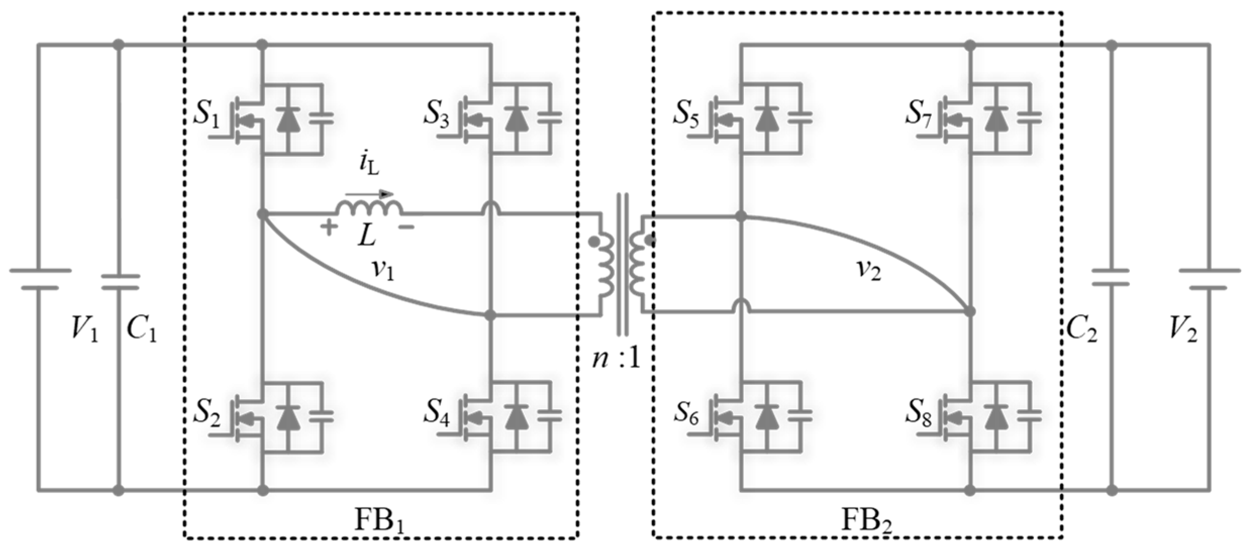
2. Analysis Modeling and Operational Analysis of DAB Converters
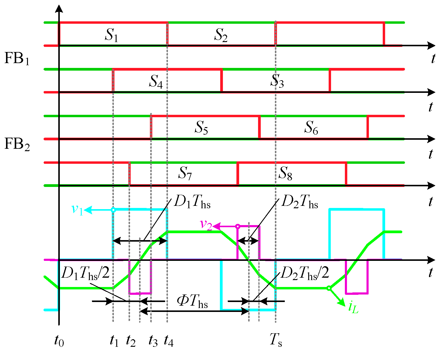
2.1. Operational Mechanism of DAB Converters
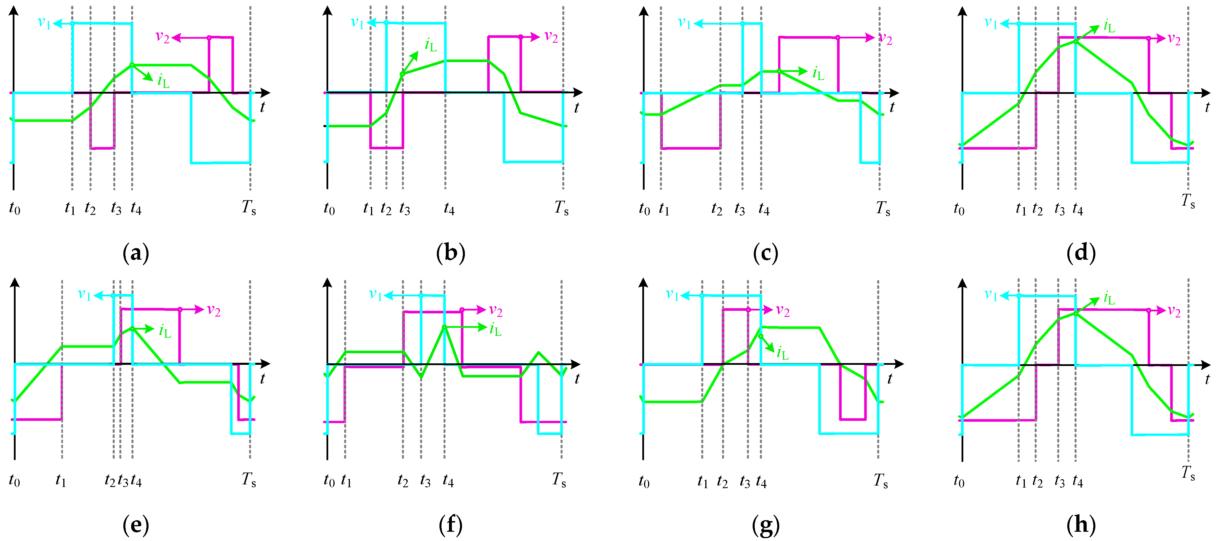
2.2. Classification and Selection of TPS Modes in DAB Converters
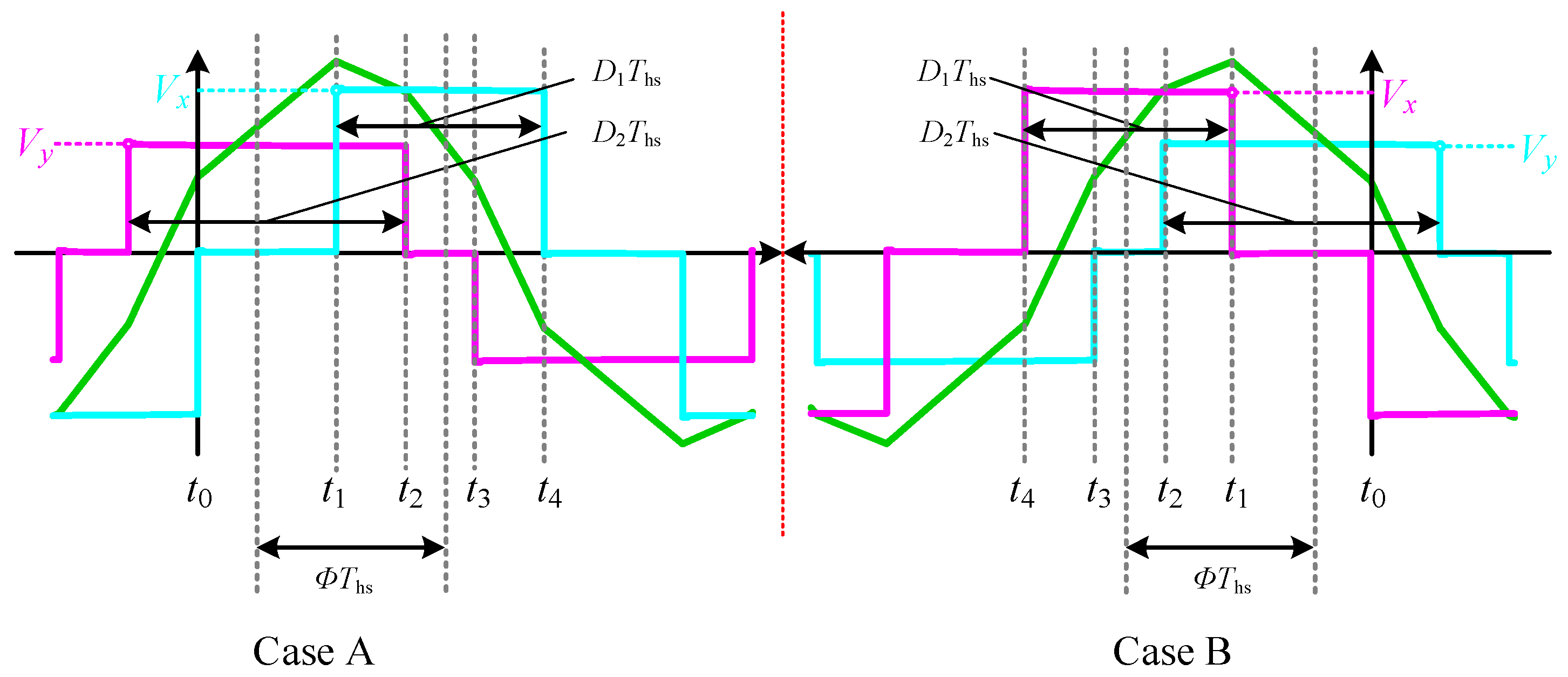
2.3. Symmetry of DAB Converters
3. Principle of Proposed SOS-TPS
3.1. Modulation Strategy in the Low-Power Range When k > 1
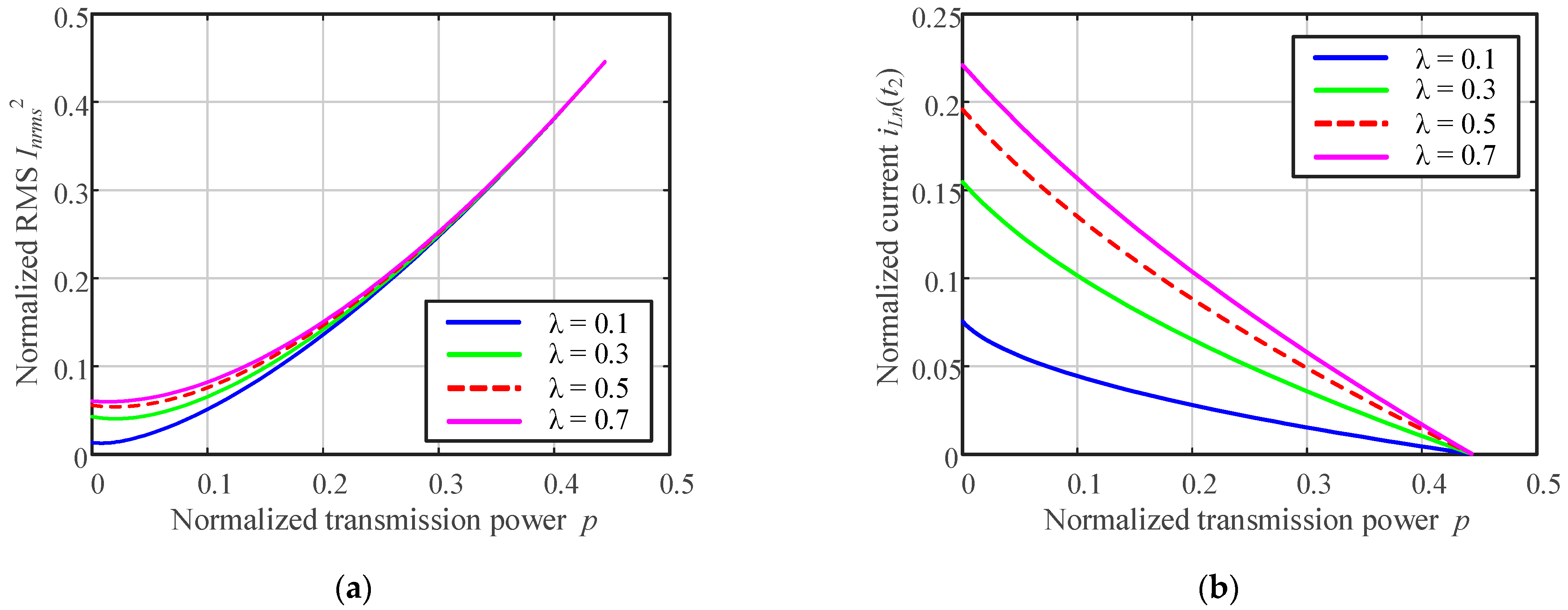
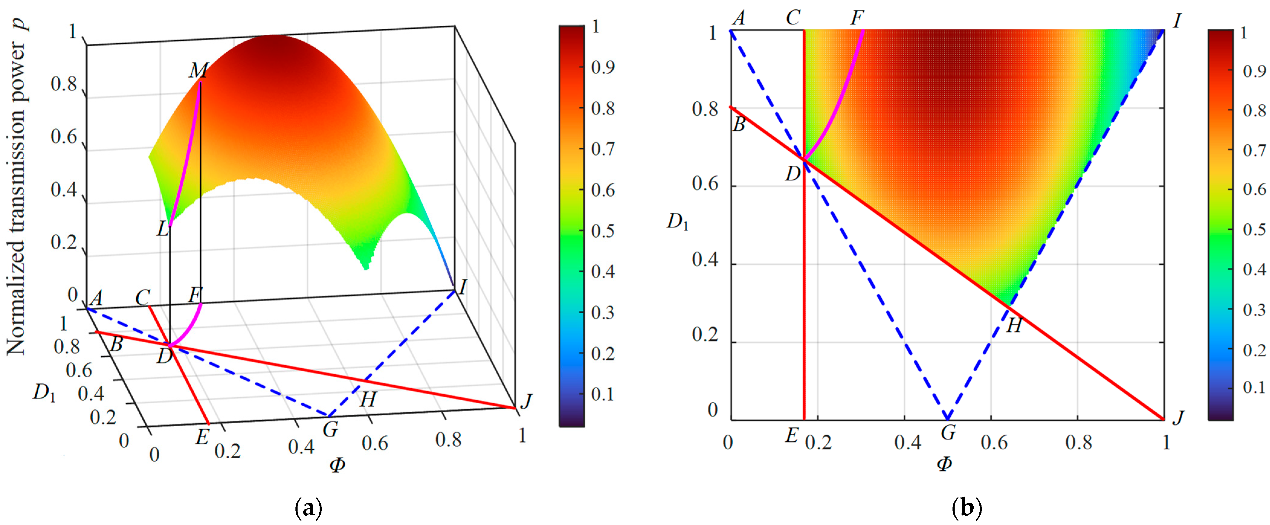
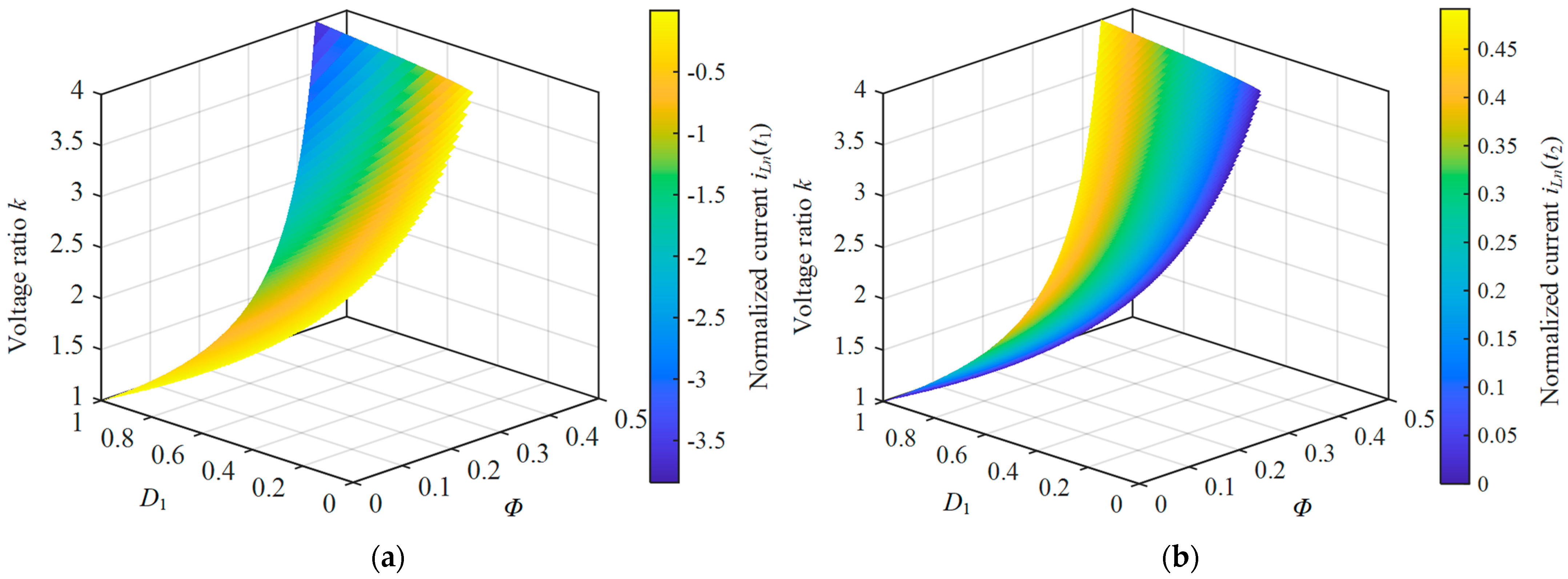
3.2. Modulation Strategy in Medium-Power Range When k > 1
3.3. Modulation Strategy in the High-Power Range When k > 1
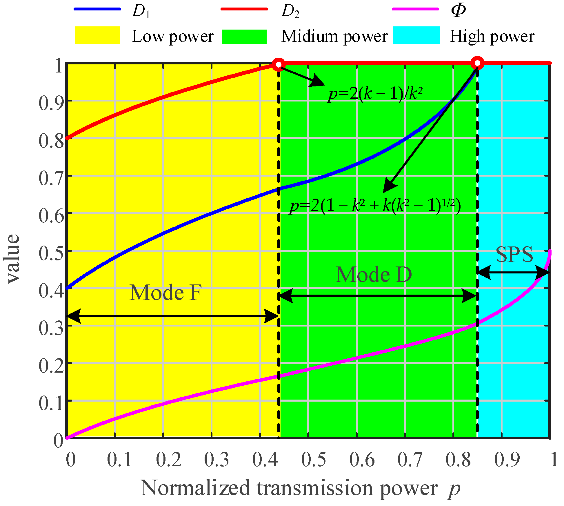
3.4. Synopsis of the SOS-TPS Strategy for DAB Converters
4. Comparative Analysis of ZVS Range and RMS Current in Existing Schemes
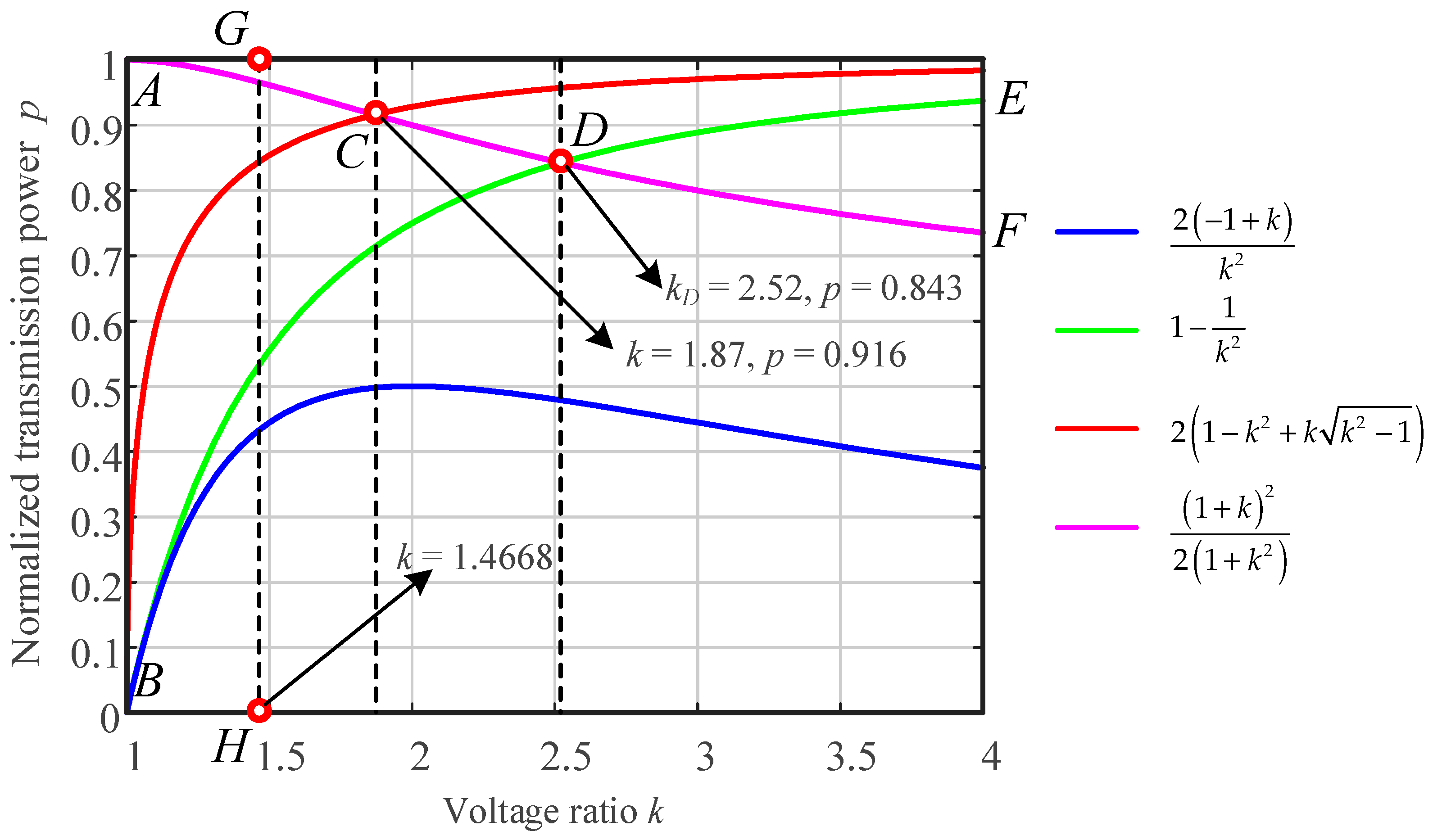
4.1. ZVS Range
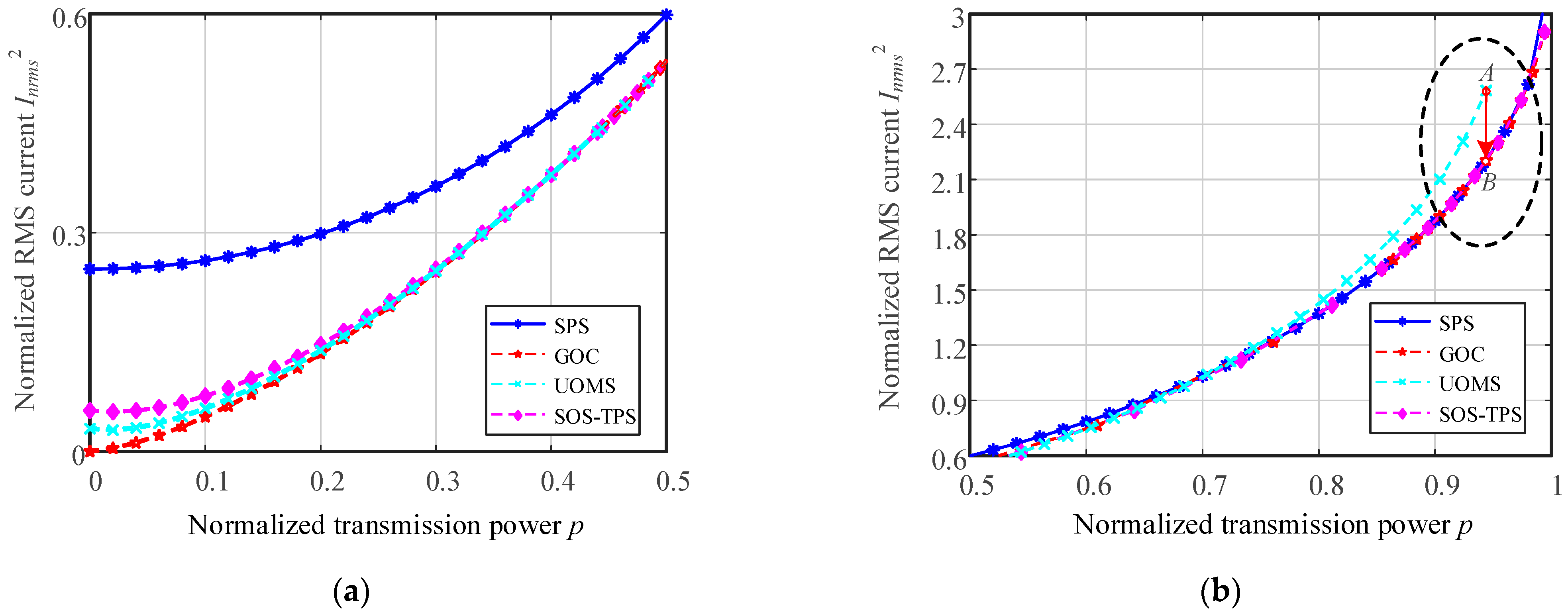
4.2. RMS Current
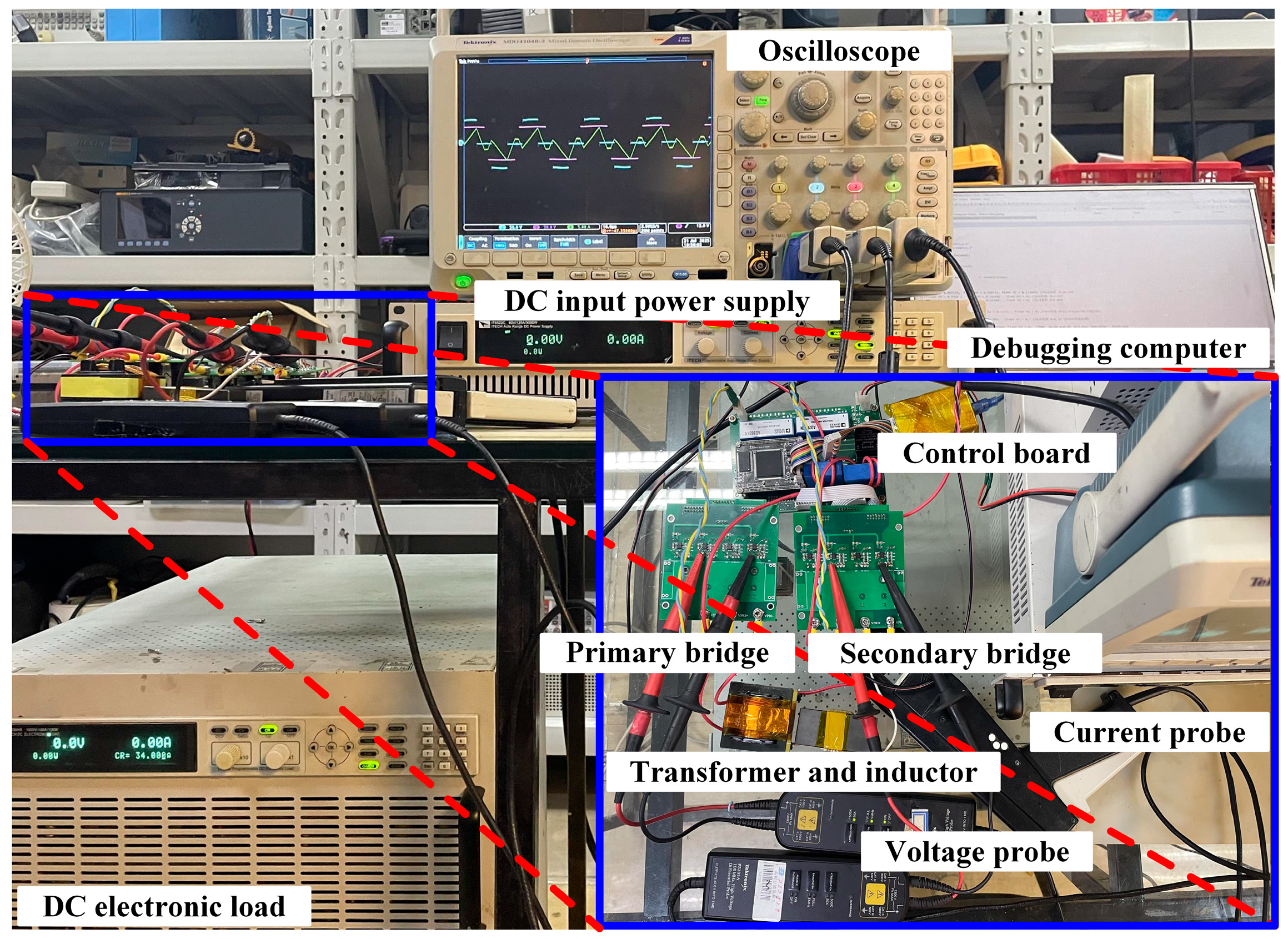
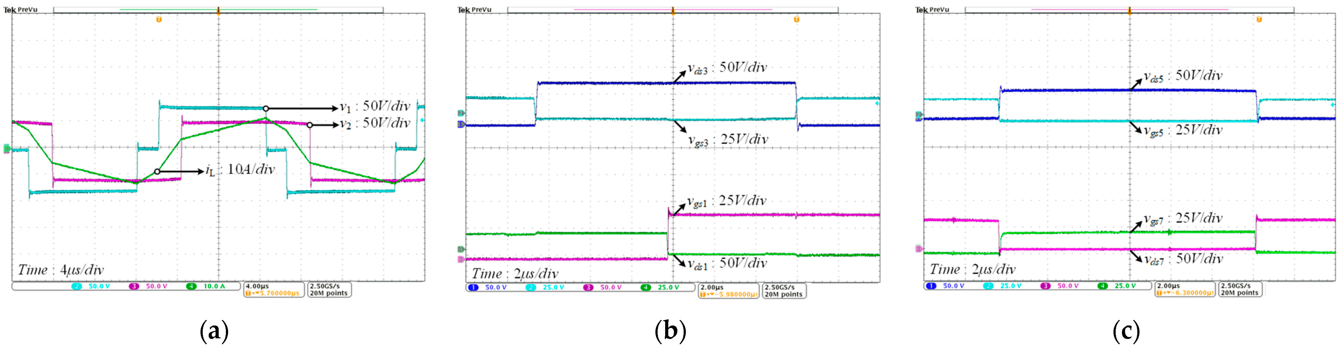
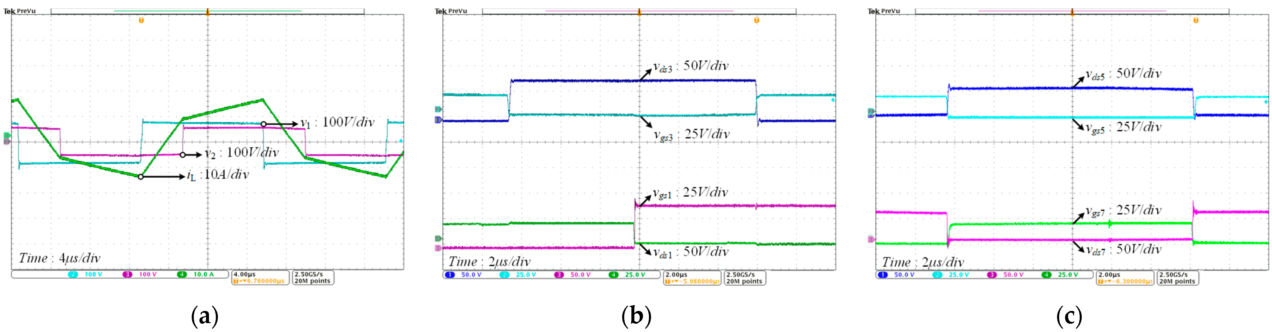
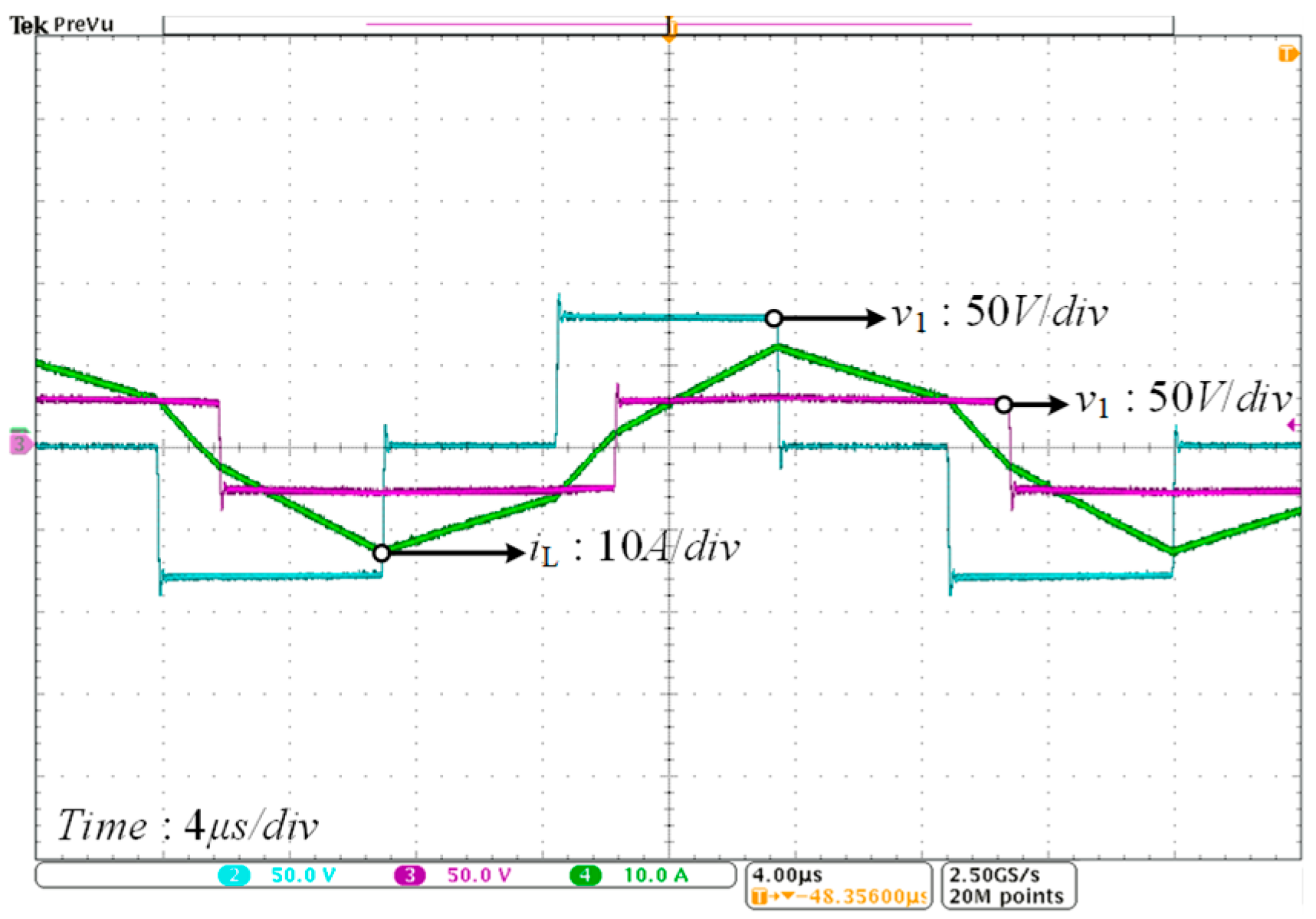
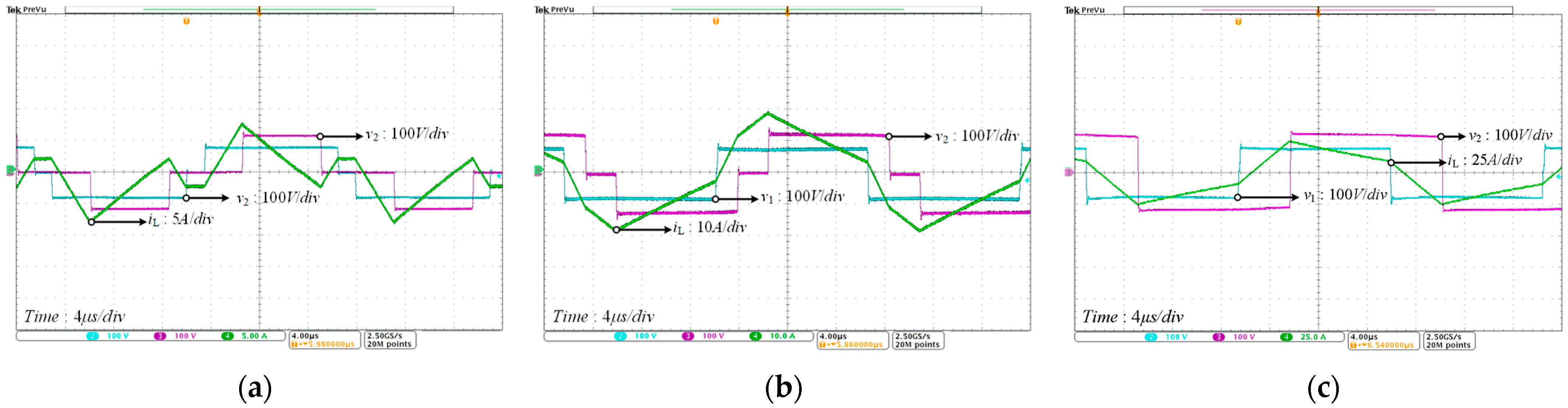
5. Experimental Verification
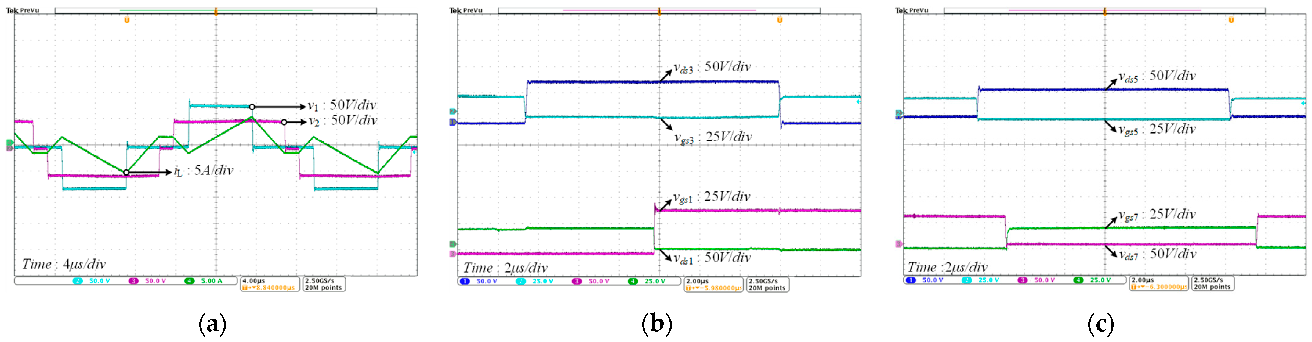
5.1. Experimental Verification with k > 1
5.2. Experimental Verification with k < 1
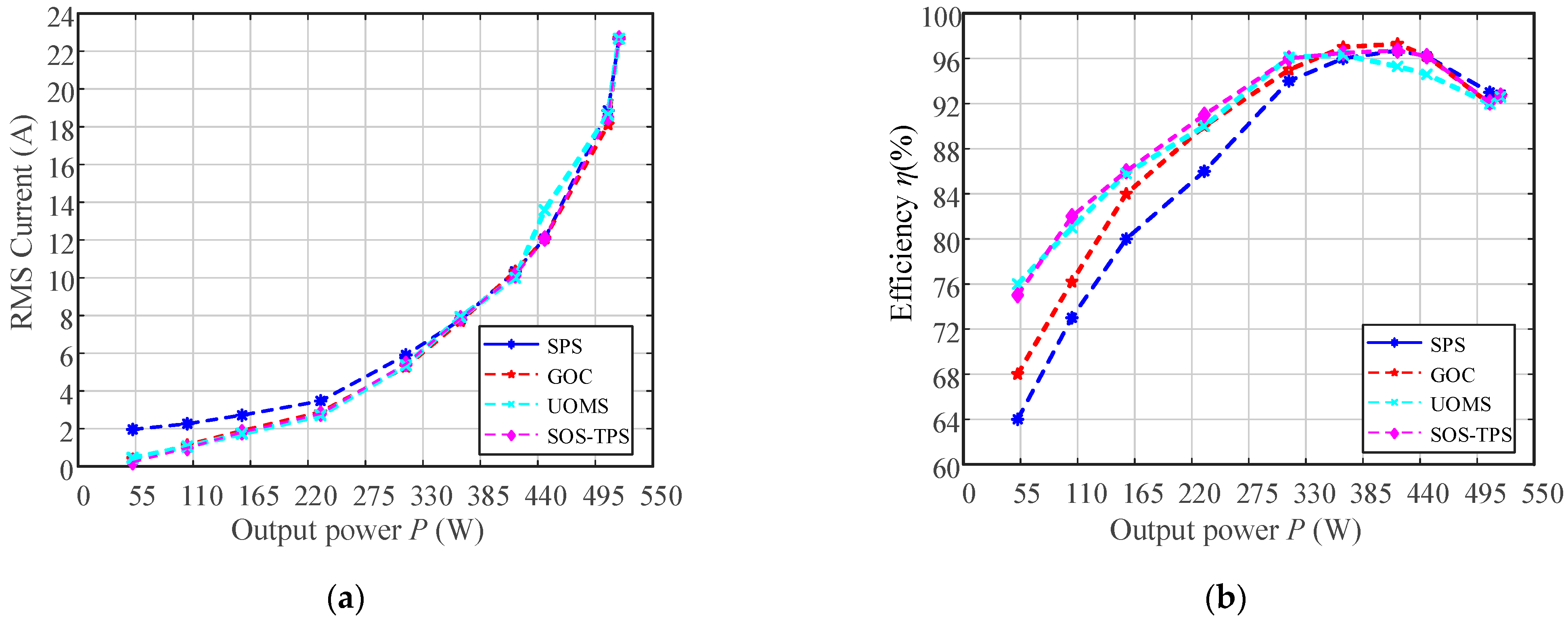
5.3. RMS Current and Efficiency
6. Conclusions
Author Contributions
Funding
Data Availability Statement
Acknowledgments
Conflicts of Interest
Abbreviations
| DAB | Dual-active bridge (converter) |
| TPS | Triple-phase shift modulation |
| SOS-TPS | Symmetric optimization strategy based on triple-phase shift |
| RMS | Root mean square |
| ZVS | Zero-voltage switching |
| KKT | Karush–Kuhn–Tucker (conditions) |
| LMM | Lagrange multiplier method |
| SPS | Single-phase shift modulation |
| DPS | Dual-phase shift modulation |
| EPS | Extended-phase shift modulation |
| DOFs | Degree of freedoms |
| WBG | Wide bandgap |
| EMC | Electromagnetic compatibility |
| UOMS | Unified optimal modulation strategy |
| GOC | Global optimal condition |
| RL | Reinforcement learning |
| ANN | Artificial neural network |
| AI | Artificial intelligence |
| PSO | Particle swarm optimization |
| FIS | Fuzzy inference system |
References
- Hou, N.; Li, Y.W. A Tunable Power Sharing Control Scheme for the Output-Series DAB DC-DC System With Independent or Common Input Terminals. IEEE Trans. Power Electron. 2019, 34, 9386–9391. [Google Scholar] [CrossRef]
- Tian, J.; Zhuo, C.; Wang, F.; Deng, H. Dual-Side Asymmetric Duty Modulation Based on Accurate Soft-Switching Characteristics Modeling for DAB-Based DC Microgrid. IEEE J. Emerg. Sel. Top. Power Electron. 2024, 12, 3146–3160. [Google Scholar] [CrossRef]
- Gou, Y.; Zhuo, F.; Wang, F.; Yu, K.; Zhan, C.; Xia, B. Lifetime Estimation of SiC Power Modules in DAB Converter Over Wide-Load Range Considering the Temperature-Dependent Characteristics. IEEE J. Emerg. Sel. Top. Power Electron. 2024, 12, 156–171. [Google Scholar] [CrossRef]
- Tian, J.; Zhuo, C.; Wang, F.; Deng, H. An RMS Current Minimization Method for Three-Level ANPC-DAB-Based Distributed Energy Storage System With Full Operation ZVS. IEEE J. Emerg. Sel. Top. Power Electron. 2024, 12, 2388–2405. [Google Scholar] [CrossRef]
- Li, C.; Liu, J.; Du, S.; Dang, H.; Deng, Z.; Chen, H. A T-Type DAB-Based Isolated DC-DC-AC Three-Port Converter With High Power Efficiency. IEEE Trans. Power Electron. 2023, 38, 14178–14194. [Google Scholar] [CrossRef]
- Shah, S.S.; Iyer, V.M.; Bhattacharya, S. Exact Solution of ZVS Boundaries and AC-Port Currents in Dual Active Bridge Type DC-DC Converters. IEEE Trans. Power Electron. 2019, 34, 5043–5047. [Google Scholar] [CrossRef]
- Pan, X.; Rathore, A.K. Novel Bidirectional Snubberless Naturally Commutated Soft-Switching Current-Fed Full-Bridge Isolated DC/DC Converter for Fuel Cell Vehicles. IEEE Trans. Ind. Electron. 2014, 61, 2307–2315. [Google Scholar]
- Xu, G.; Sha, D.; Xu, Y.; Liao, X. Hybrid-Bridge-Based DAB Converter With Voltage Match Control for Wide Voltage Conversion Gain Application. IEEE Trans. Power Electron. 2018, 33, 1378–1388. [Google Scholar] [CrossRef]
- Xu, D.H.; Zhao, C.H.; Fan, H.F. A PWM plus phase-shift control bidirectional DC-DC converter. IEEE Trans. Power Electron. 2004, 19, 666–675. [Google Scholar] [CrossRef]
- Mahdavifard, M.; Mazloum, N.; Zahin, F.; KhakparvarYazdi, A.; Abasian, A.; Khajehoddin, S.A. An Asymmetrical DAB Converter Modulation and Control Systems to Extend the ZVS Range and Improve Efficiency. IEEE Trans. Power Electron. 2022, 37, 12774–12792. [Google Scholar] [CrossRef]
- Wang, M.; Wei, S.; Mou, D.; Wu, P. Research on Efficient Single-Sided Asymmetric Modulation Strategy for Dual Active Bridge Converters in Wide Voltage Range. IEEE J. Emerg. Sel. Top. Power Electron. 2022, 10, 5738–5748. [Google Scholar] [CrossRef]
- Krismer, F.; Kolar, J.W. Accurate Small-Signal Model for the Digital Control of an Automotive Bidirectional Dual Active Bridge. IEEE Trans. Power Electron. 2009, 24, 2756–2768. [Google Scholar] [CrossRef]
- Bai, H.; Mi, C. Eliminate Reactive Power and Increase System Efficiency of Isolated Bidirectional Dual-Active-Bridge DC-DC Converters Using Novel Dual-Phase-Shift Control. IEEE Trans. Power Electron. 2008, 23, 2905–2914. [Google Scholar] [CrossRef]
- Zhao, B.; Yu, Q.; Sun, W. Extended-Phase-Shift Control of Isolated Bidirectional DC-DC Converter for Power Distribution in Microgrid. IEEE Trans. Power Electron. 2012, 27, 4667–4680. [Google Scholar] [CrossRef]
- Yu, H.; Hang, L.; Zheng, X.; He, Z.; He, Y.; Shen, L.; Shao, C.; Zeng, P.; Wu, Q.; Yang, X.; et al. Globally Unified ZVS and Quasi-Optimal Minimum Conduction Loss Modulation of DAB Converters. IEEE Trans. Transp. Electrif. 2022, 8, 3989–4000. [Google Scholar] [CrossRef]
- Hou, N.; Song, W.S.; Wu, M.Y. Minimum-Current-Stress Scheme of Dual Active Bridge DC-DC Converter With Unified Phase-Shift Control. IEEE Trans. Power Electron. 2016, 31, 8552–8561. [Google Scholar] [CrossRef]
- Huang, J.; Wang, Y.; Li, Z.; Lei, W. Unified Triple-Phase-Shift Control to Minimize Current Stress and Achieve Full Soft-Switching of Isolated Bidirectional DC-DC Converter. IEEE Trans. Ind. Electron. 2016, 63, 4169–4179. [Google Scholar] [CrossRef]
- Gu, Q.; Yuan, L.; Nie, J.; Sun, J.; Zhao, Z. Current Stress Minimization of Dual-Active-Bridge DC-DC Converter Within the Whole Operating Range. IEEE J. Emerg. Sel. Top. Power Electron. 2019, 7, 129–142. [Google Scholar] [CrossRef]
- An, F.; Song, W.; Yang, K.; Luo, S.; Feng, X. Optimised power control and balance scheme for the output parallel dual-active-bridge DC-DC converters in power electronic traction transformer. IET Power Electron. 2019, 12, 2295–2303. [Google Scholar] [CrossRef]
- Li, L.; Xu, G.; Xiong, W.; Liu, D.; Su, M. An Optimized DPS Control for Dual-Active-Bridge Converters to Secure Full-Load-Range ZVS With Low Current Stress. IEEE Trans. Transp. Electrif. 2022, 8, 1389–1400. [Google Scholar] [CrossRef]
- Li, J.; Luo, Q.M.; Mou, D.; Wei, Y.Q.; Zhang, X.Y. Comprehensive Optimization Modulation Scheme of Low Current Level and Wide ZVS Range for Dual Active Bridge Converter With Dead-Zone Control. IEEE Trans. Power Electron. 2022, 37, 2731–2748. [Google Scholar] [CrossRef]
- Chaurasiya, S.; Singh, B. A Load Adaptive Hybrid DPS Control for DAB to Secure Minimum Current Stress and Full ZVS Operation Over Wide Load and Voltage Conversion Ratio. IEEE Trans. Ind. Appl. 2023, 59, 1901–1911. [Google Scholar] [CrossRef]
- Li, X.; Zhang, X.; Lin, F.; Sun, C.; Mao, K. Artificial-Intelligence-Based Triple Phase Shift Modulation for Dual Active Bridge Converter With Minimized Current Stress. IEEE J. Emerg. Sel. Top. Power Electron. 2023, 11, 4430–4441. [Google Scholar] [CrossRef]
- Tian, J.; Wang, F.; Zhuo, F.; Cui, X.; Yang, D. An Optimal Primary-Side Duty Modulation Scheme With Minimum Peak-to-Peak Current Stress for DAB-Based EV Applications. IEEE Trans. Ind. Electron. 2023, 70, 6798–6808. [Google Scholar] [CrossRef]
- Jia, D.; Wang, D. Current Stress Minimization Based on Particle Swarm Optimization for Dual Active Bridge DC-DC Converter. Actuators 2024, 13, 421. [Google Scholar] [CrossRef]
- Cheng, S.; Wang, F.; Han, Z.; Zhang, C. DAB unified ZVS control strategy with optimal current stress in full power range under TPS control. IET Power Electron. 2024, 17, 2405–2415. [Google Scholar] [CrossRef]
- Naseem, H.; Seok, J.-K. Reactive Power Controller for Single Phase Dual Active Bridge DC–DC Converters. IEEE Access 2023, 11, 141537–141546. [Google Scholar] [CrossRef]
- Zhang, L.; Tu, C.; Xiao, F.; Liu, B.; Li, P. Intrinsic Regularity Analysis and Optimization Control of Current Stress and RMS for Dual-Active Bridge Converter. Electronics 2024, 13, 4802. [Google Scholar] [CrossRef]
- Gong, L.; Jin, X.; Xu, J.; Deng, Z.; Li, H.; Soeiro, T.B.; Wang, Y. A Dynamic ZVS-Guaranteed and Seamless-Mode-Transition Modulation Scheme for the DAB Converter That Maximizes the ZVS Range and Lowers the Inductor RMS Current. IEEE Trans. Power Electron. 2022, 37, 13119–13134. [Google Scholar] [CrossRef]
- Shi, H.; Wen, H.; Chen, J.; Hu, Y.; Jiang, L.; Chen, G. Minimum-Reactive-Power Scheme of Dual-Active-Bridge DC-DC Converter With Three-Level Modulated Phase-Shift Control. IEEE Trans. Ind. Appl. 2017, 53, 5573–5586. [Google Scholar] [CrossRef]
- Shi, H.; Wen, H.; Chen, J.; Hu, Y.; Jiang, L.; Chen, G.; Ma, J. Minimum-Backflow-Power Scheme of DAB-Based Solid-State Transformer With Extended-Phase-Shift Control. IEEE Trans. Ind. Appl. 2018, 54, 3483–3496. [Google Scholar] [CrossRef]
- Li, S.; Yuan, X.; Wang, Z.; Wang, K.; Zhang, Y.; Wu, X. A Unified Optimal Modulation Strategy for DAB Converters to Tradeoff the Backflow Power Reduction and All ZVS in the Full Operating Range. IEEE J. Emerg. Sel. Top. Power Electron. 2023, 11, 5701–5723. [Google Scholar] [CrossRef]
- Krismer, F.; Kolar, J.W. Closed Form Solution for Minimum Conduction Loss Modulation of DAB Converters. IEEE Trans. Power Electron. 2012, 27, 174–188. [Google Scholar] [CrossRef]
- Everts, J.; Krismer, F.; Van den Keybus, J.; Driesen, J.; Kolar, J.W. Optimal ZVS Modulation of Single-Phase Single-Stage Bidirectional DAB AC-DC Converters. IEEE Trans. Power Electron. 2014, 29, 3954–3970. [Google Scholar] [CrossRef]
- Tong, A.; Hang, L.; Li, G.; Jiang, X.; Gao, S. Modeling and Analysis of a Dual-Active-Bridge-Isolated Bidirectional DC/DC Converter to Minimize RMS Current With Whole Operating Range. IEEE Trans. Power Electron. 2018, 33, 5302–5316. [Google Scholar] [CrossRef]
- Li, J.; Luo, Q.; Mou, D.; Wei, Y.; Sun, P.; Du, X. A Hybrid Five-Variable Modulation Scheme for Dual-Active-Bridge Converter With Minimal RMS Current. IEEE Trans. Ind. Electron. 2022, 69, 336–346. [Google Scholar] [CrossRef]
- Xie, H.; Cai, F.; Jiang, J.; Li, D. A Fundamental Harmonic Analysis-Based Optimized Scheme for DAB Converters With Lower RMS Current and Wider ZVS Range. IEEE Trans. Transp. Electrif. 2023, 9, 4045–4058. [Google Scholar] [CrossRef]
- Li, X.; Zhang, X.; Lin, F.; Sun, C.; Mao, K. Artificial-Intelligence-Based Hybrid Extended Phase Shift Modulation for the Dual Active Bridge Converter With Full ZVS Range and Optimal Efficiency. IEEE J. Emerg. Sel. Top. Power Electron. 2023, 11, 5569–5581. [Google Scholar] [CrossRef]
- Zhao, B.; Song, Q.; Liu, W. Efficiency Characterization and Optimization of Isolated Bidirectional DC-DC Converter Based on Dual-Phase-Shift Control for DC Distribution Application. IEEE Trans. Power Electron. 2013, 28, 1711–1727. [Google Scholar] [CrossRef]
- Liu, X.; Zhu, Z.Q.; Stone, D.A.; Foster, M.P.; Chu, W.Q.; Urquhart, I.; Greenough, J. Novel Dual-Phase-Shift Control With Bidirectional Inner Phase Shifts for a Dual-Active-Bridge Converter Having Low Surge Current and Stable Power Control. IEEE Trans. Power Electron. 2017, 32, 4095–4106. [Google Scholar] [CrossRef]
- Yan, Y.; Luo, Q.; Luo, T.; Li, J.; Xiong, J.; Xiao, H. Current Stress Optimized Strategy for the Dual-Active-Bridge Converter With Triple-Phase-Shift and Variable DC-Link Voltage Control. IEEE Trans. Power Electron. 2025, 40, 8344–8355. [Google Scholar] [CrossRef]
- Zhang, J.; Sha, D.; Song, K. Single-Phase Single-Stage Bidirectional DAB AC-DC Converter With Extended ZVS Range and High Efficiency. IEEE Trans. Power Electron. 2023, 38, 3803–3811. [Google Scholar] [CrossRef]
- Cui, L.; Zhang, Y.; Wang, X.; Zhang, D. An Enhanced Integrated Optimization Strategy for Wide ZVS Operation and Reduced Current Stress Across the Full Load Range in DAB Converters. Appl. Sci. 2025, 15, 7413. [Google Scholar] [CrossRef]


| Mode | Normalized Root Mean Square Current Values |
|---|---|
| D | |
| F | |
| G |
| Operating Conditions | V1 | V2 | Duty Cycles of the Primary Voltage Waveforms | Duty Cycles of the Secondary-Side Voltage Waveforms |
|---|---|---|---|---|
| a | Vx | Vy | D1 | D2 |
| b | Vy | Vx | D2 | D1 |
| c | Vm | Vn | D2 | D1 |
| Modes | Low-Power Range | Medium-Power Range | High-Power Range |
|---|---|---|---|
| k > 1 | |||
| k < 1 | |||
| Items | Specifications |
|---|---|
| Operating Condition Configuration | Input port: V1 = 80 V |
| Output port: V2 = 26.66 V, 53.33 V, 120 V, 240 V | |
| Switching Frequency | Fs = 40 kHz |
| Switches | S1–S8: C3M0075120K VDSS = 1200 V, ID = 32 A, Rds(on) = 75 mΩ, Coss = 58 pF |
| Inductor | Inductance: 25.5 µH |
| Transformer | Turns Ratio n = 1 |
| Controller | TMS320F28335 |
| Filter Capacitor | C1 = C2 = 600 µF |
Disclaimer/Publisher’s Note: The statements, opinions and data contained in all publications are solely those of the individual author(s) and contributor(s) and not of MDPI and/or the editor(s). MDPI and/or the editor(s) disclaim responsibility for any injury to people or property resulting from any ideas, methods, instructions or products referred to in the content. |
© 2025 by the authors. Licensee MDPI, Basel, Switzerland. This article is an open access article distributed under the terms and conditions of the Creative Commons Attribution (CC BY) license (https://creativecommons.org/licenses/by/4.0/).
Share and Cite
Cui, L.; Zhang, Y.; Wang, X.; Zhang, D. Symmetric Optimization Strategy Based on Triple-Phase Shift for Dual-Active Bridge Converters with Low RMS Current and Full ZVS over Ultra-Wide Voltage and Load Ranges. Electronics 2025, 14, 3031. https://doi.org/10.3390/electronics14153031
Cui L, Zhang Y, Wang X, Zhang D. Symmetric Optimization Strategy Based on Triple-Phase Shift for Dual-Active Bridge Converters with Low RMS Current and Full ZVS over Ultra-Wide Voltage and Load Ranges. Electronics. 2025; 14(15):3031. https://doi.org/10.3390/electronics14153031
Chicago/Turabian StyleCui, Longfei, Yiming Zhang, Xuhong Wang, and Dong Zhang. 2025. "Symmetric Optimization Strategy Based on Triple-Phase Shift for Dual-Active Bridge Converters with Low RMS Current and Full ZVS over Ultra-Wide Voltage and Load Ranges" Electronics 14, no. 15: 3031. https://doi.org/10.3390/electronics14153031
APA StyleCui, L., Zhang, Y., Wang, X., & Zhang, D. (2025). Symmetric Optimization Strategy Based on Triple-Phase Shift for Dual-Active Bridge Converters with Low RMS Current and Full ZVS over Ultra-Wide Voltage and Load Ranges. Electronics, 14(15), 3031. https://doi.org/10.3390/electronics14153031