Article

Modelling and Simulation of a New π-Gate AlGaN/GaN HEMT with High Voltage Withstand and High RF Performance

School of Microelectronics, Changzhou University, Changzhou 213164, China
*
Author to whom correspondence should be addressed.
Electronics 2025, 14(15), 2947; https://doi.org/10.3390/electronics14152947
Submission received: 22 June 2025 / Revised: 17 July 2025 / Accepted: 22 July 2025 / Published: 24 July 2025

Abstract

Aiming at the problems of low withstand voltage and poor RF performance of traditional HEMT devices, a new AlGaN/GaN high electron mobility transistor device with a π-gate (NπGS HEMT) is designed in this paper. The new structure incorporates a π-gate design along with a PN-junction field plate and an AlGaN back-barrier layer. The device is modeled and simulated in Silvaco TCAD 2015 software and compared with traditional t-gate HEMT devices. The results show that the NπGS HEMT has a significant improvement in various characteristics. The new structure has a higher peak transconductance of 336 mS·mm−1, which is 13% higher than that of the traditional HEMT structure. In terms of output characteristics, the new structure has a higher saturation drain current of 0.188 A/mm. The new structure improves the RF performance of the device with a higher maximum cutoff frequency of about 839 GHz. The device also has a better performance in terms of voltage withstand, exhibiting a higher breakdown voltage of 1817 V. These results show that the proposed new structure could be useful for future research on high voltage withstand and high RF HEMT devices.

1. Introduction

In recent years, III-V nitride materials have attracted much attention along with the rapid growth of the semiconductor industry. Due to its wide forbidden band, strong electron mobility, and exceptional resistance to high voltage, the semiconductor material of third-generation wide-band gallium nitride (GaN) has gained popularity as a research topic [1,2]. GaN materials have a forbidden bandwidth of approximately 3.4 eV, significantly higher than the 1.1 eV of traditional silicon (Si) materials, which allows GaN to maintain stable operation at high voltages and temperatures [3,4,5]. In addition, GaN has a higher saturation electron rate and electron mobility, which makes GaN-based devices perform well in high-frequency applications, achieving faster switching speeds and lower on-resistance [6,7,8]. As a result, GaN devices perform better in high-frequency and high-power environments. However, traditional silicon materials struggle to compete with GaN materials due to their narrower bandwidth and lower electron mobility [9,10].
In this context, AlGaN/GaN heterojunctions further enhance the electrical properties of GaN materials. For AlGaN/GaN heterojunctions, due to the lattice mismatch and polarization properties between AlGaN and GaN materials, at the interface, a high-density two-dimensional electron gas (2DEG) is developed, which can have an electron density as high as 1013 cm−3 without any doping [11,12,13,14]. Unlike traditional Si devices that require the introduction of carriers through doping, 2DEG in AlGaN/GaN heterojunctions is formed naturally through the polarization effect, which avoids the ion-scattering effect caused by doping and thus maintains extremely high electron mobility [15,16,17,18,19]. This high-density 2DEG not only significantly improves the device’s conductivity and frequency response characteristics but also enhances its voltage tolerance, making the AlGaN/GaN HEMT especially suitable for high-frequency and high-power applications [20,21,22,23].
The study of RF and voltage withstand performance of GaN-based HEMT devices has received much attention in recent years. The researchers started from the breakdown voltage of the AlGaN/GaN HEMT to give play to the high-voltage characteristics of GaN materials. Domestic and foreign researchers have proposed a variety of methods. The current application of the technology includes the metal field plate structure, the buffer dopant layer, the superlattice buffer layer, the back-barrier technology, and the substrate transfer technology, etc. [24,25]. For example, in 2000, a research group at the University of California reported that they had grown device structures with gate field plates in GaN HEMT devices with a stacked shape. The length between the drain and the gate of the HEMT was 13 μm, and the final device breakdown voltage achieved was 570 V. Still, the frequency characteristics of the whole device were degraded considerably. In 2004, Xing et al. innovatively proposed a HEMT with a multilayer field plate structure [26]. On top of the initial layer of metal field plate, the structure develops a second layer, which changes a single electric field spike in the channel into three lower electric field peaks. Experimental measurements reveal that the double-layer gate field plate structure’s breakdown voltage is 900 V. However, the frequency capabilities of the final device are significantly degraded due to the fact that the introduction of the metal field plate substantially improves the parasitic capacitance in devices. In 2010, Eldad’s group reported a GaN HEMT device with C doping in the buffer layer of the device [27]. This structure optimizes the balance between on-resistance and current collapse, and the breakdown voltage can reach more than 1000 V with sub-threshold leakage current suppression and low on-resistance. However, the presence of deep energy level traps results in a substantial degradation of the device’s DC characteristics, which usually manifests itself as a current collapse. In these studies, the breakdown characteristics of HEMT have been improved; at the same time, side effects such as increased parasitic capacitance and deterioration of DC characteristics have been produced. Therefore, research to ensure high RF performance along with high voltage withstand performance is essential for GaN-based HEMT devices [28,29,30].
A new AlGaN/GaN high electron mobility transistor device with a π-gate (NπGS HEMT) is designed in this paper. The device employs a PN-junction field plate and a π-gate structure to attenuate the electric field accumulation in the channel near the gate and, at the same time, to pull up the surface electric field value in the channel between the gate and the drain, which ultimately improves the voltage withstand characteristics of the device. In addition, a new structure of back-barrier layer and symmetric π-gate HEMT is adopted to overcome the increase in parasitic capacitance due to the field plate and asymmetric π-gate and to increase the withstand voltage while maintaining the superiority of frequency characteristics. Meanwhile, this paper simulates the traditional t-gate HEMT and the new structure of π-gate HEMT by comparing the difference between the two structures in their transfer characteristics, output characteristics, breakdown characteristics, and RF characteristics. The new structure is analyzed to have higher peak transconductance, higher saturation leakage current, higher maximum cutoff frequency, and higher breakdown voltage. The new structure can be well suited for high RF and high withstand voltage operating environments. It is very helpful for future research on high electron mobility devices.

2. Theoretical Approach and Modelling

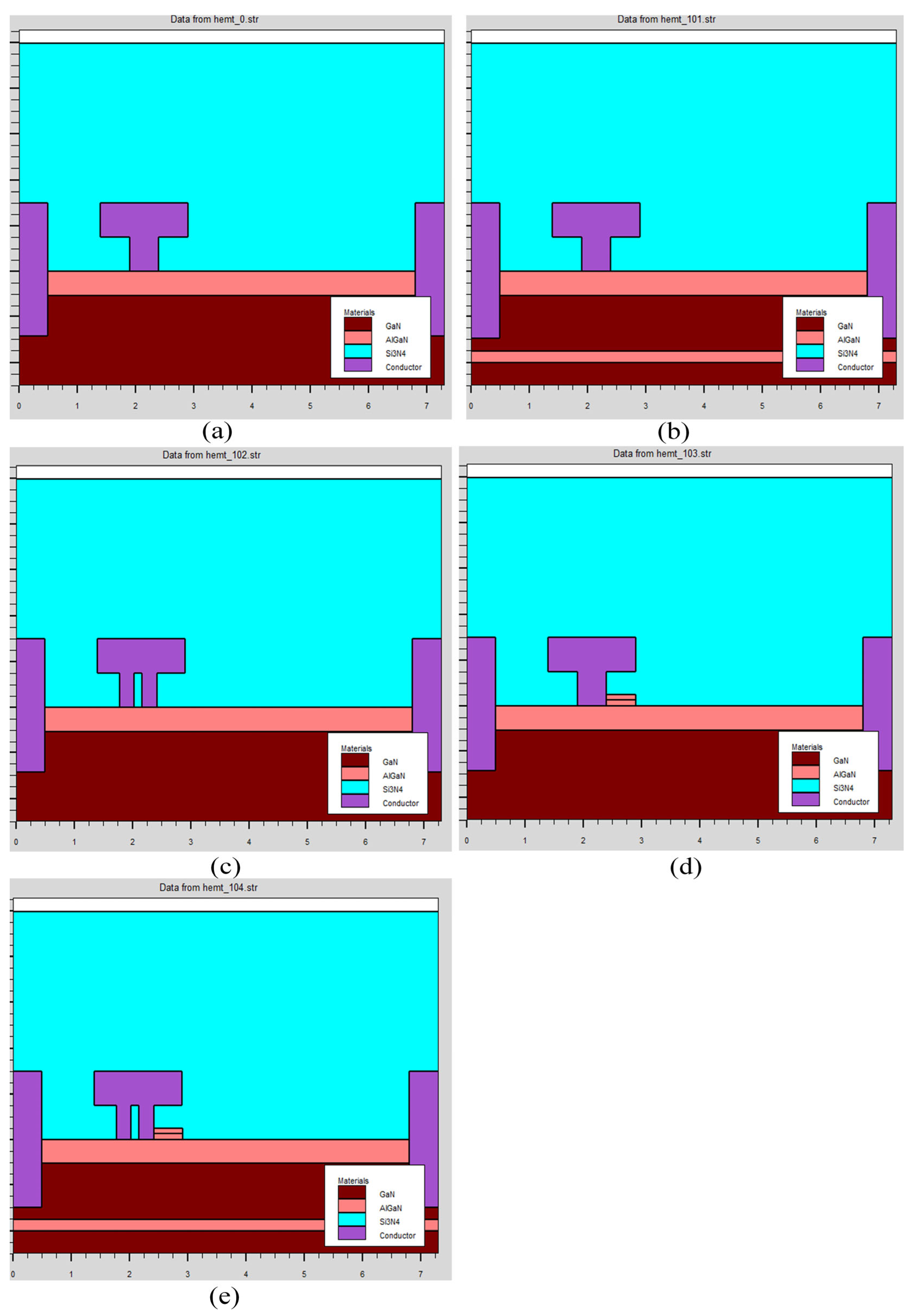
2.1. Device Structure and Theoretical Approach

Figure 1 shows the structural schematic of the new π-gate AlGaN/GaN HEMT proposed in this paper. The device is structured from the bottom up as follows: AlGaN back-barrier layer, GaN buffer layer, AlGaN barrier layer, SiN passivation layer, and PN-junction field plate, and also has the source, gate, and drain of a traditional HEMT device. The new structure is applied as a depletion device. The primary parameters of the device are shown in Table 1. The device structures used in this paper have had preliminary process realizations reported in some of the structures, such as the π-gate structure and the PN junction injection technique, both of which have experimental precedents and provide a reference basis for subsequent practical preparation studies. In GaN semiconductor materials, there are two non-centrosymmetric crystal structures, namely, wurtzite and zincblende. Of these two structures, the wurtzite structure is less symmetric. In the absence of external stress, the separation of positive and negative charge centers within the GaN crystal produces a polarization phenomenon along the polar axis, also known as the spontaneous polarization effect of GaN [31]. Under external stress, the crystal undergoes lattice deformation, separating positive and negative charges inside and forming an electric field, which induces a polarized charge on the crystal surface, triggering the piezoelectric effect.
The spontaneous polarization of AlGaN materials is affected by the Al component x:
P s p ( x ) = ( 0.052 x 0.029 )
The expression for piezoelectric polarization is as follows:
P P E = 2 ( a a 0 ) / a 0 a 0 ( e 31 e 33 C 13 C 33 )
where a0 is the lattice constant characterizing the equilibrium state, (aa0)/a0 is the isotropic plane strain component, C13 and C33 are elastic coefficients, and e31 and e33 are the piezoelectric coefficients.
Since the AlGaN material possesses a wider energy gap than the GaN material, the energy band at the interface junction of the heterojunction bends when reaching equilibrium, forming a triangular potential [32]. On the GaN side, the energy at the bottom of the conduction band is already smaller than the Fermi energy level EF; therefore, there will be a large number of electrons gathered in the triangular potential well. Meanwhile, a high potential barrier exists on the AlGaN side of the wide bandgap, making it difficult for electrons to cross the boundary of the potential well, and they are confined to lateral motion within a thin layer at the interface, which is referred to as the two-dimensional electron gas. If the drain-source voltage VDS is artificially applied, a transverse electric field is formed inside the channel, and this field drives the 2D electron gas along the heterojunction interface, leading to the generation of the drain output current IDS. The new structure retains the advantages of both RF and breakdown performance, and a comparison of the performance of NπGS with that of a representative GaN HEMT from recent years is shown in Table 2 [33,34,35,36]. From Table 2, it can be found that most structures focus on breakdown while ignoring the structure’s effect on RF, and the new structure compensates for this shortcoming.

2.2. Physical Modelling

To guarantee the correctness of the simulation results, the Silvaco TCAD model must be calibrated as part of the device simulation process. We use Wang and his team’s suggested correction technique in this simulation [37]. Firstly, given the polarization effects present in the GaN HEMT model, accurately calibrating this polarization model throughout the simulation phase is crucial. In the modeling of polarization effects, the tensor piezoelectric model and the spontaneous polarization model were enabled. For GaN, the spontaneous polarization was set to −0.029 C/m2 and the piezoelectric coefficients were e31 = −0.49 C/m2 and e33 = 0.73 C/m2. For AlGaN, the polarization parameters were obtained by linearly interpolating between the values for GaN and AlN, based on the aluminum composition. For instance, when the Al content is 0.25, the spontaneous polarization is approximately −0.046 C/m2 and the corresponding piezoelectric coefficients are approximately e31 ≈ −0.58 C/m2 and e33 ≈ 1.1 C/m2. Next, for mobility modeling, the ANALYTIC model provided by Silvaco was used, and the low-field saturation drift velocity was set to 2 × 107 cm/s to make sure that the 2DEG mobility saturated at a low field matches the true data. The extent of the influence of these two parameters on the device performance was experimentally verified. In addition to this, in order to realize the Schottky contact at the gate, we define the gate figure of merit as 5.2 eV. To create the ohmic contact, below the drain and source, a significant amount of n-type Gaussian doping is introduced. It is shown that the semiconductor surface charge density distribution can be changed by adjusting the doping concentration, thus affecting the device’s performance. According to this model, the passivation materials Si3N4 and air have relative dielectric coefficients of 7.5 and 1.0, and the charge transfer rate at the interface was calculated by using the charge separation theory, which allows us to obtain the gas concentration versus time curves as well as the corresponding electron density distributions at different temperatures. In this paper, we consider this effect. A model design of a composite trap is presented. Setting the trap type to donor, with the energy level located approximately 0.3 eV below the conduction band and a trap density of 1 × 1012 cm−2 eV−1. The composition x of Al(x)Ga(1−x)N is 0.25. We note that in Al(x)Ga(1−x)N, the value of x could be a crucial factor in determining the spin properties and transport performance of AlGaN/GaN HEMT devices [38]. Ultimately, a parallel model relating to the electric field needs to be constructed to ensure that the mobility of the electrons is consistent with the distribution model of the electric field.

3. Results and Discussions

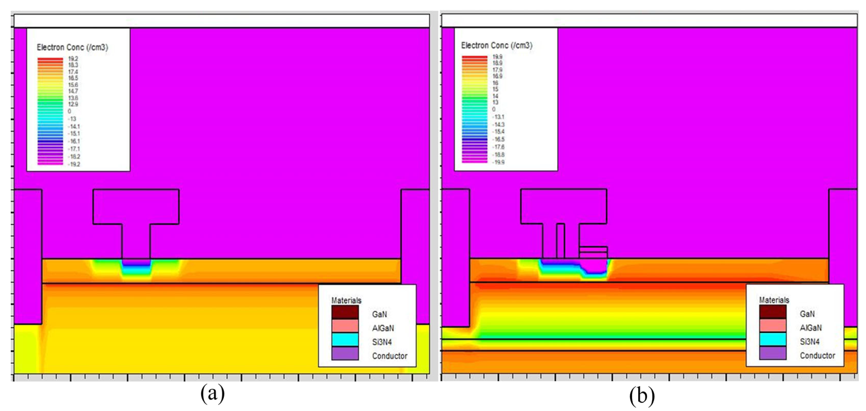
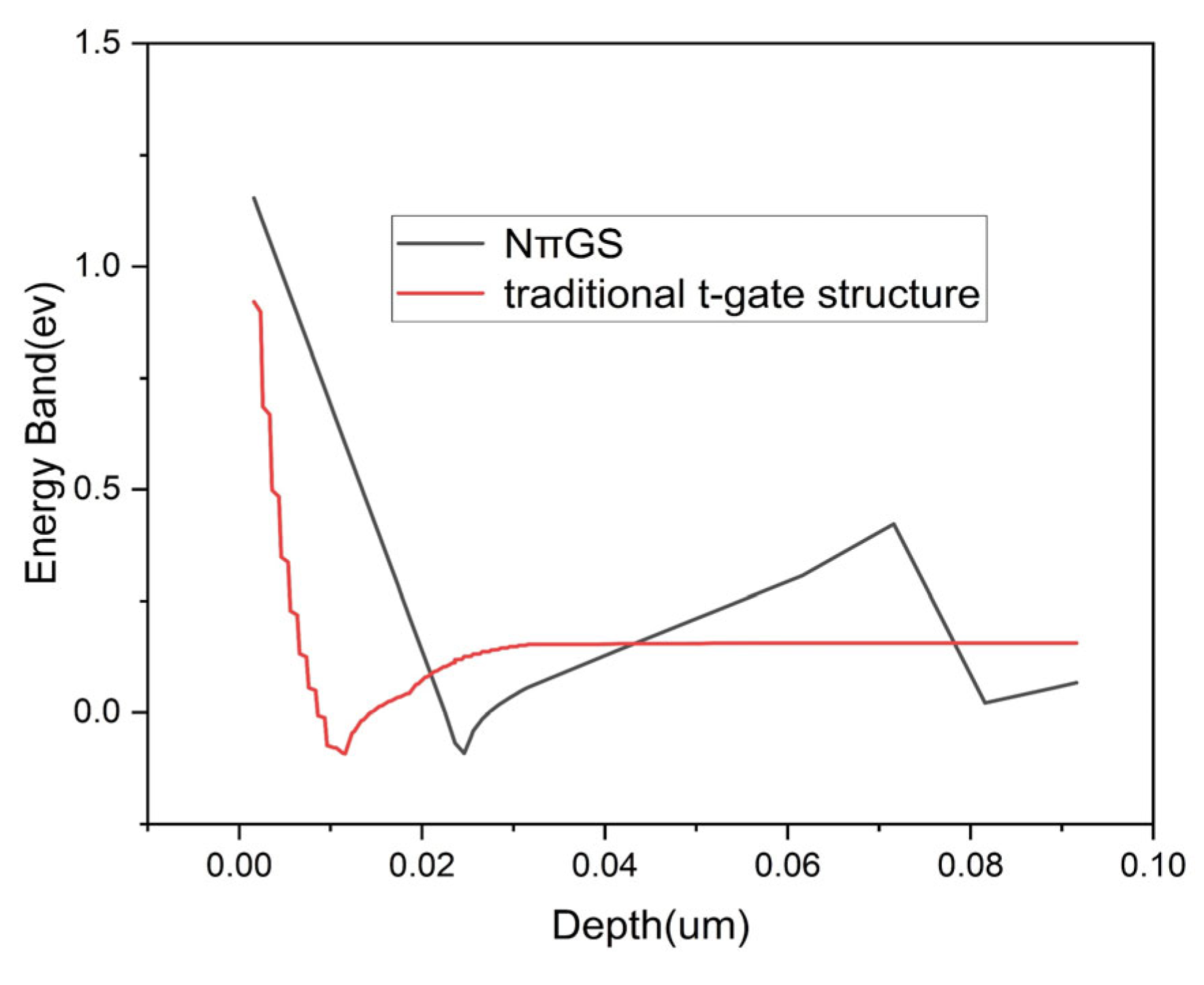
3.1. Device Characteristics

Regarding the upgraded new structure and the traditional t-gate structure, the simulations obtained using Silvaco TCAD are shown in Figure 2a–e. Figure 2a–d shows the 2D interface diagram of the traditional t-gate AlGaN/GaN HEMT structure, the back-barrier AlGaN/GaN HEMT structure (BBS), the π-gate AlGaN/GaN HEMT structure (πGS), and the PN-junction field plate AlGaN/GaN HEMT structure (PN-JFPS). Figure 2e shows the 2D interface diagram of the new π-gate AlGaN/GaN HEMT structure (NπGS). Figure 2a displays the conventional t-gate structure, which is not the same as the conventional t-gate structure. Because the drain and source effectively reduce the on-resistance of the device by sculpting downward by 0.06 μm [39]. We named such a construction as the conventional t-gate structure. These devices are 7.3 μm long overall. In all three structures, Figure 2a,b,d, the gate is a t-gate structure with a length of 1.5 μm and a height of 0.06 μm. In both structures, Figure 2c,e, each gate pin in the π-gate structure has a height of 0.03 μm and a gate width of 0.25 μm. It is worth noting that the lengths of the two pillars of the π-gate structure are obtained by averaging the lengths of one pillar of the t-gate structure. Furthermore, the field plate of the NπGS structure is 0.5 μm long and 0.01 μm high. Additionally, it has a 7.3 μm long by 0.01 μm high AlGaN back-barrier layer.
To ensure AlGaN/GaN HEMT devices’ performance in high-frequency and high-voltage environments, they must have a low on-resistance and a high output current [40]. However, in high-power devices, the bias region of the gate and drain tends to create a high electric field, which can rapidly reduce the on-state capability if too high a voltage causes the device to break down. Therefore, an in-depth study of this region in an on-state environment is essential. The electron concentration distribution of the conventional t-gate structure and the NπGS structure in the on-state is shown in Figure 3a,b. It can be observed that the average electron concentration of the NπGS structure is larger than that of the conventional t-gate structure, with the average electron concentration reaching a maximum of 1019.9 cm−3.
For the NπGS structure, considering that AlGaN material has a higher potential barrier than GaN material, the back-barrier layer of AlGaN further enhances the effect of the potential well on the electrons. By contrasting the 2DEG concentration of the conventional t-gate structure with that of the NπGS in the on-state, a significant increase in the 2DEG concentration of the new structure can be discernible.
This phenomenon can be illustrated more clearly from the perspective of the energy bands. Figure 4 fully demonstrates the potential well-limiting domain properties of the electrons for a 4% backed barrier layer device and a traditional device without a backed barrier layer. When an AlGaN back barrier is added, the depth of the potential well is much greater, and the width of the potential well is relatively narrow; therefore, electrons are fully confined within the potential well. This is the reason for the significant increase in 2DEG concentration in the new structure. Because the concentration of 2DEG is significantly higher compared to traditional devices, in comparison to the traditional construction, the saturation drain current of this device ought to be stronger and more consistent.

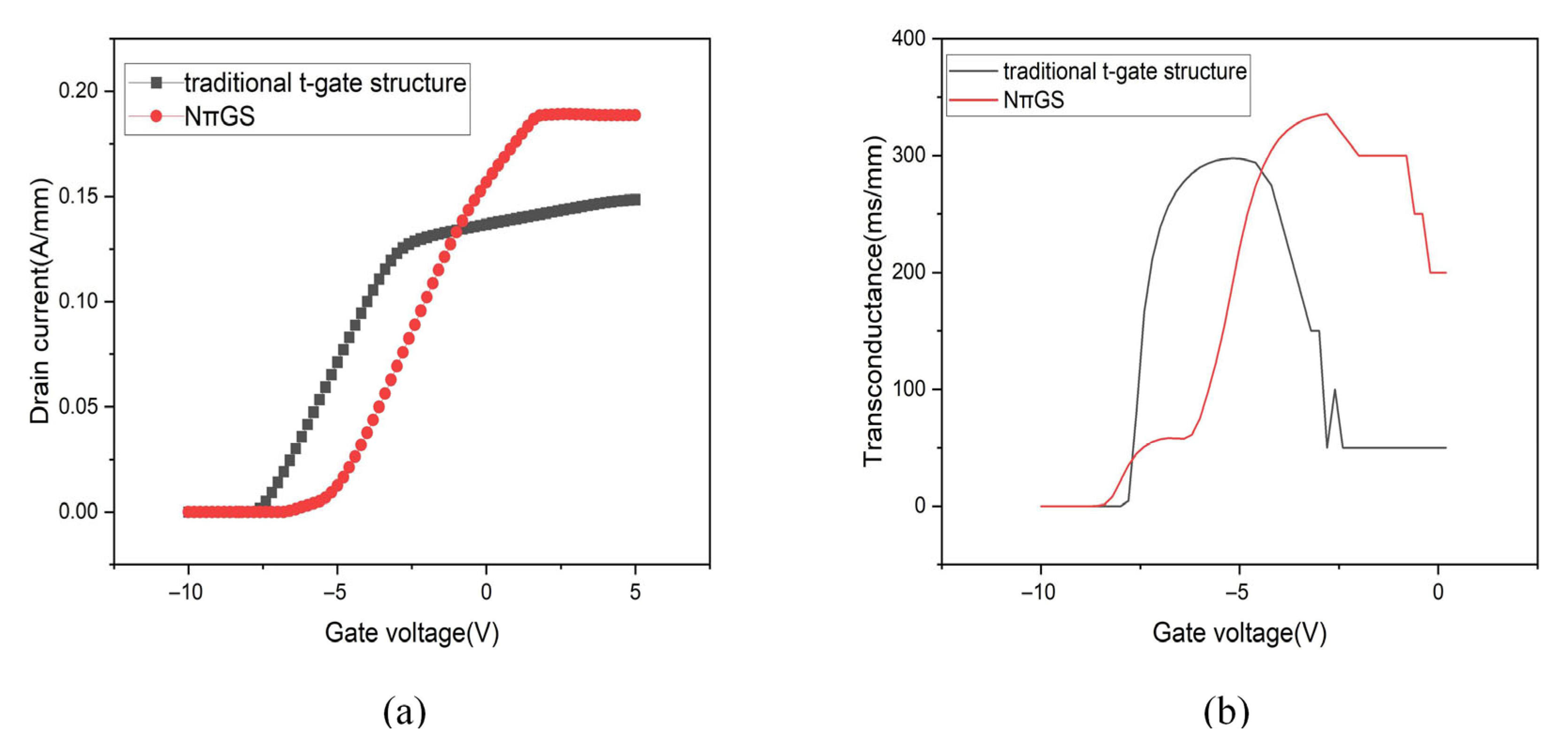
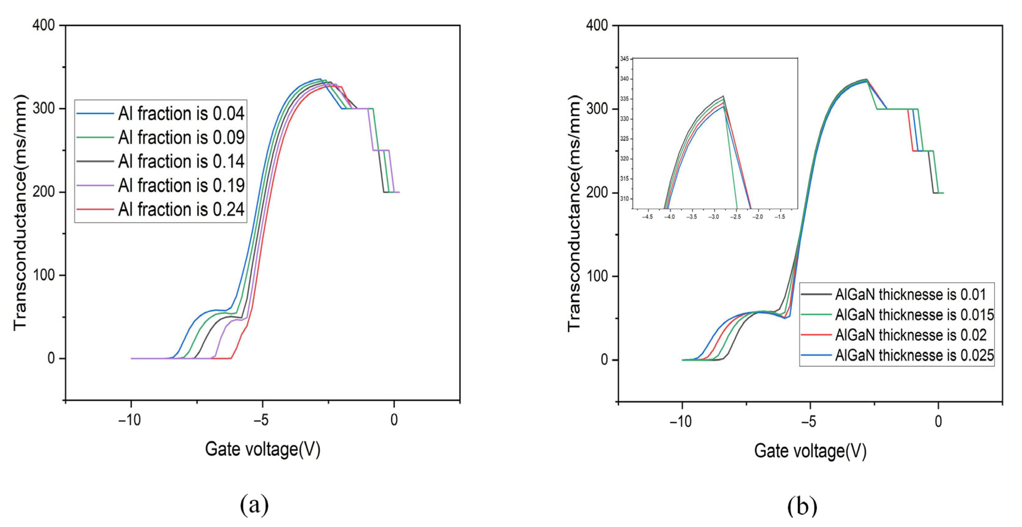
3.2. Transfer Characteristics

The transfer characteristics of two different structures are shown in Figure 5a. The following circumstances were used to assess the transfer characteristics: The source was grounded first. After that, the drain voltage is adjusted to 10 V and the gate voltage is scanned between −10 and 5 V. The maximum peak drain currents are 0.148 and 0.211 A/mm, while the threshold voltages for the conventional t-gate structure and the NπGS structure are around −7.8 and −8 V.
Regarding the conventional AlGaN/GaN HEMT depletion-type device, the variation of the heterojunction energy band diagram at different gate pressures is shown in Figure 6. If the gate voltage V g = 0 , the channel can be opened, the electrons are focused in the potential well, and the bottom of the conduction band is below the Fermi energy level. When the gate voltage V g > 0 , more electrons are focused in the two-dimensional potential well as the Fermi energy level increases. The device shuts off and the potential well progressively vanishes, the 2DEG is exhausted, the conduction band’s bottom climbs above the Fermi energy level when the gate voltage V g < 0 . Devices with the addition of the AlGaN back-barrier layer have a positive threshold voltage drift, because of the enhanced negative polarization effect of the back-barrier and the enhanced 2DEG depletion. However, since the π-gate enhances the control of the channel by extending the gate above the source and drain regions, it optimizes the electric field distribution, making it possible to effectively turn on the channel at lower gate voltages and lowering the threshold voltage. Therefore, the threshold voltage of the NπGS structure is only slightly larger than that of the traditional structure.
One of the measurements of the AlGaN/GaN HEMT devices that shows the Schottky gate’s channel control is the transconductance. It is one of the most significant factors in assessing the device’s transfer capabilities. The greater the transconductance value, the more current that the device can drive at the same voltage supplied to the gate. The peak transconductance of the NπGS structure with the addition of an AlGaN back barrier is higher, as shown in Figure 5b; the peak transconductance is 336 mS·mm−1 when the thickness of the back barrier is 0.01 μm. The connection between the transconductance and the gate voltage bias can also be acquired from the transfer capabilities. The maximum transconductance of the device can also be calculated from Equation (3) as g m = 336 mS·mm−1.
g m = I d V g | V d = c o n s t
where ID is the drain current, VD is the drain voltage, and VG is the gate voltage.
The peak transconductance is increased by about 13% in comparison with the traditional device, and the linearity becomes better. The enhanced domain-limiting effect of the AlGaN back-barrier layer on the 2DEG results in a sharper response of the electrons to the gate. Higher peak transconductance eventually results from the gate’s improved control of the 2DEG. Figure 7a,b shows the transconductance curves of the NπGS structure under the AlGaN back-barrier layer with different Al fractions and the transconductance curves of the NπGS structure with different thicknesses of the AlGaN back-barrier layer. From Figure 7a, it can be seen that the device transconductance decreases faster as the Al component increases. This is due to the appearance of parasitic channels; the buffer layer leakage becomes larger, while the interface scattering is enhanced, the traps increase, and the electron mobility decreases. Whereas, in device modeling, the drain current can usually be expressed as shown in Equation (4):
I D = q · n s · u n · v D S L · W
where n s is the carrier concentration per unit area, q is the electron charge, u n is the electron mobility, L is the channel length, V D S is the drain-source voltage, and W is the channel width.
Substituting I D in Equation (4) into Equation (3) yields Equation (5):
g m = q · u n · V D S L · W · n s V G S
From Equation (5), it can be obtained that transconductance and electron mobility are positively correlated; therefore, the transconductance of the new structure gradually decreases. From Figure 7b, when the thickness of the back barrier increases, it causes the appearance of parasitic channels, resulting in a decrease in transconductance. Therefore, both parameters need a value that makes the most sense.

3.3. Output Characteristics

The output characteristic curves of the BBS structure, traditional t-gate structure, NπGS structure, and πGS structure are shown in Figure 8a. One of the primary metrics used to quantify the output characteristics is the largest saturation drain current. Based on the outcomes of the simulation, it can be found that the NπGS structure has a larger maximum saturation drain current than the other three structures. When the gate-source voltage is 0 V and the drain-source voltage is 10 V, the largest saturation drain currents of the NπGS structure, the BBS structure, the πGS structure, and the traditional t-gate structure are about 0.188, 0.117, 0.139, and 0.130 A/mm. The maximum saturation drain currents of the NπGS structure are increased by about 44.6% in contrast to the traditional t-gate construction. Because the AlGaN back-barrier layer further improves the domain-limiting nature of the potential wells for electrons. Devices with the addition of an AlGaN back barrier have deeper potential wells and narrower potential well widths, and electrons are completely confined in the potential wells. The two-dimensional electron gas concentration is much higher than that of the traditional devices, which leads to a significant increase in the saturation drain current of the new construction. This is the same conclusion we drew from the energy band diagram. The reason for the relatively higher saturation drain current of the π-gate structure compared to the t-gate structure can be explained by Equation (6):
I D S = 1 2 μ e f f C o x ( V G S V t h ) 2
where IDS is the drain-to-source current, Cox is the gate oxide capacitance, μeff is the effective carrier mobility, VGS is the gate-source voltage, and Vth is the threshold voltage.
It can be seen from the equation that the higher the effective carrier mobility, the higher the saturation current of the HEMT. Since the construction of the π-gate enables the gate to cover a wider area, it is possible to distribute the gate’s electric field more uniformly. The more uniform electric field distribution reduces the local electric field enhancement phenomenon, which reduces the scattering of electrons below the gate and increases the effective carrier mobility of electrons. This ultimately results in a higher saturation drain current for the πGS structure than for the t-gate structure. The innovations in both parts, the back barrier and the π-gate, act together on the NπGS structure, which significantly raises the new structure’s drain current. This further confirms that the structural design of the NπGS greatly optimizes the output characteristics of the device.
Experimentally, it is found that both the thickness of the AlGaN back-barrier layer and the Al component have a strong influence on the device output characteristics. As shown in Figure 8b, as the Al component increases, the saturation drain current of the device becomes smaller and smaller due to the emergence of parasitic channels. The parasitic channel can be seen from the energy band diagram in Figure 4. The formation of parasitic channels, usually due to improper material interfaces or doping distribution in heterostructure devices, results in the formation of “unintended” conductive paths due to the presence of additional electrons or holes in regions of undesired carriers beyond the dominant conductive channel. This results in larger leakage in the device buffer layer, enhanced interfacial scattering, increased traps, and, consequently, decreased electron mobility. The electron mobility is directly proportional to the saturation drain current, and it eventually causes the saturation drain current to drop. Therefore, an Al fraction of 4% is chosen as the optimal value here. Figure 8c shows that with the increasing thickness of the AlGaN back-barrier layer, the saturation current is gradually decreasing. Because the thicker the AlGaN back-barrier layer is, the AlGaN layer will gradually be in the relaxation state, the polarization effect is weakened, the concentration of 2DEG decreases, and the current density decreases. Therefore, the saturation leakage current is lower as the thickness increases. However, the relative influence of the Al component is small, and the thickness of the AlGaN back-barrier layer is chosen here to be the best at 0.01 μm.

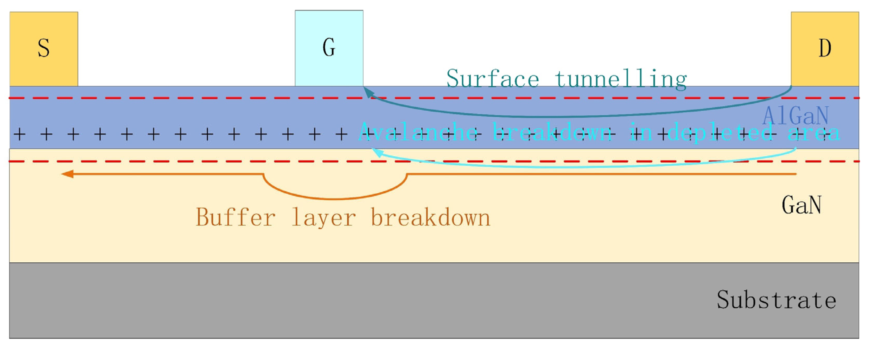
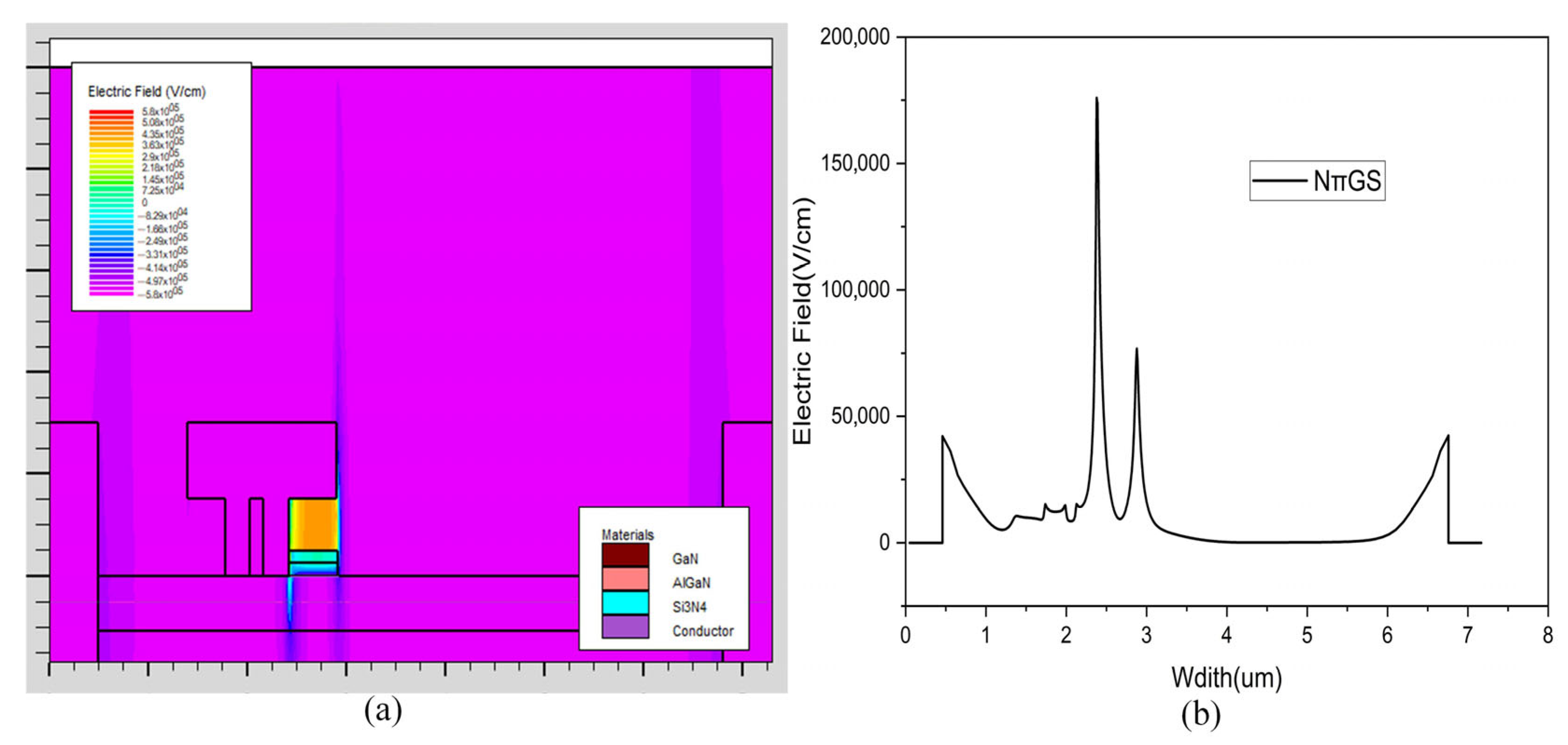
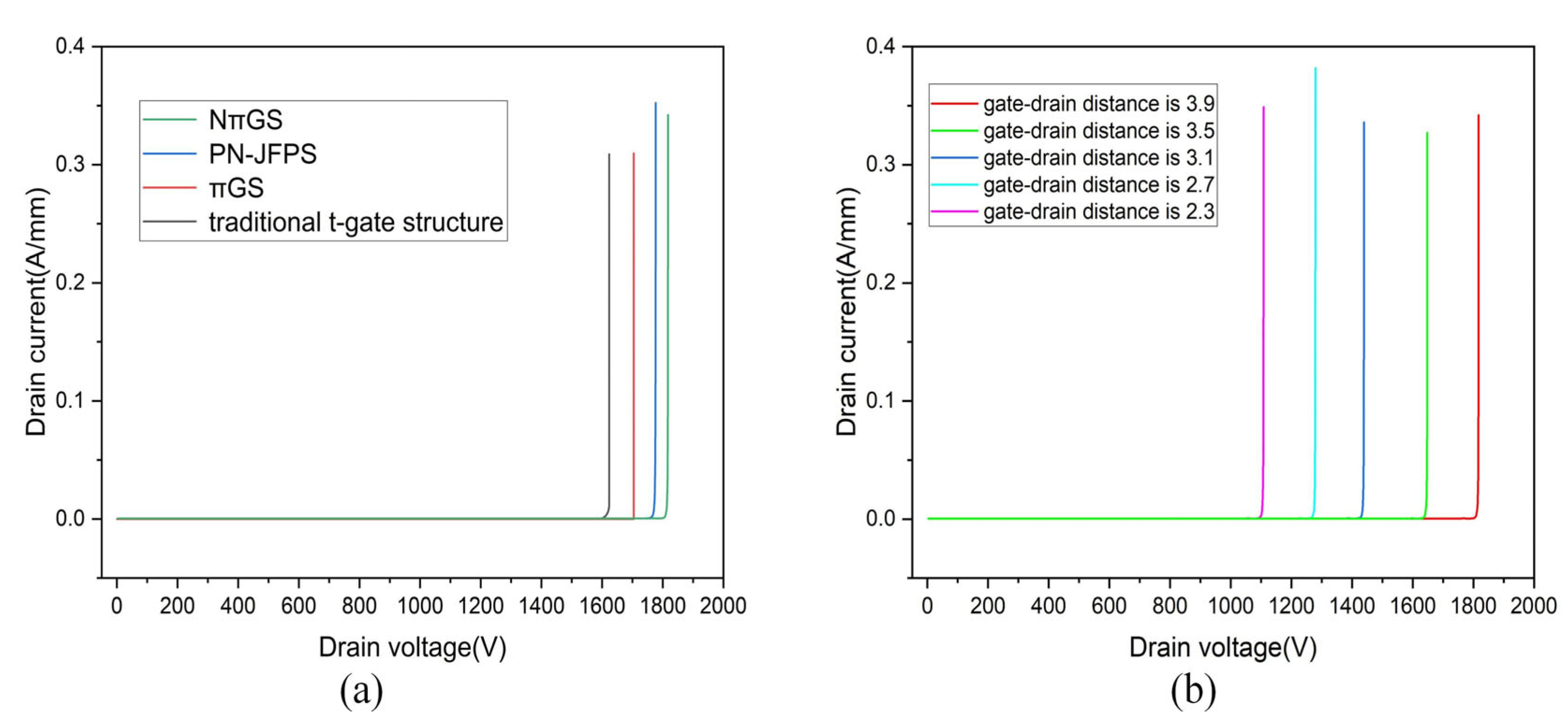
3.4. Breakdown Characteristics

According to the report summary, GaN HEMT has three main breakdown mechanisms, as shown in Figure 9: The first is the presence of current leakage in the buffer layer, resulting in device breakdown. The second is the presence of current leakage at the gate, resulting in device breakdown. The third is avalanche breakdown when the device channel is under the action of a strong electric field.
At present, the main factor limiting the improvement of GaN HEMT voltage withstand capability is the electric field concentration phenomenon at the edge of the gate. Because of collisional ionization under the acceleration of a high electric field, a lot of hole-electron pairs are created in the device’s channel, which eventually causes avalanche breakdown. The traditional device breakdown voltage can be obtained from Equation (7):
V b r e a k d o w n = E c r i t · d q
where Vbreakdown indicates the breakdown voltage, q indicates the meta-charge, d indicates the distance from the critical region in the device, and Ecrit indicates the critical electric field strength.
It can be observed that the breakdown voltage of the device and the electric field strength are closely related. The drain current is at a very low level before the device breaks down; when the voltage rises to a critical value, the current rises sharply, showing a nearly vertical jump characteristic, and the corresponding voltage at this time is defined as the breakdown voltage. Figure 10 and Figure 11 show the electric field maps below the NπGS gate and the 2D electric field contour maps of the NπGS before and after the device breakdown. The electric field distribution in Figure 10 and Figure 11 can be further verified: before breakdown, the electric field intensity in the critical region of the device is significantly lower than the extreme value of the electric field after breakdown, indicating that the point is in the critical state of avalanche breakdown. Therefore, we identify this voltage as the breakdown voltage of the device accordingly [41]. Secondly, to define avalanche breakdown at the level of physical mechanisms, a shock ionization model should be added in conjunction with the avalanche ionization rate or the enhanced behavior of the electric field under reverse bias.
Considering the four structures’ transfer characteristics, to make sure the channel is in the off state, the voltages of the NπGS structure, the PN-JFPS structure, the πGS structure, and the conventional t-gate structure are installed below their threshold voltages. Subsequently, until the device breaks down, the drain voltage was progressively raised from 0 V. The breakdown characteristics of four different AlGaN/GaN HEMT devices are shown in Figure 12a. The breakdown voltages of the NπGS structure, the PN-JFPS structure, the πGS structure, and the conventional t-gate structure are 1817, 1766, 1704, and 1623 V, respectively. In contrast to the conventional t-gate structure, the PN-JFPS structure HEMT has a PN-junction field plate at the gate edge, and the n-type side of the PN-junction field plate has a doping concentration that is 2–3 orders of magnitude smaller than the p-type side. The 2DEG in the channel below the PN-junction is depleted, lowering the 2DEG concentration in the channel. Because the depletion zone of the PN-junction stretches along the low-concentration doped n-type side to the AlGaN/GaN heterojunction channel. Concurrently, the depletion region in the channel is extended, and most of the drain voltage is applied to the depletion region of the PN-junction, weakening the aggregation of the electric field in the channel near the gate and modulating the electric field distribution in the channel. Therefore, the device’s voltage withstand characteristics are improved. By dividing the peak electric field from the gate edge towards the drain area into many peaks, the πGS structure modifies the structure’s electric field distribution. Finally, the πGS structure reduces the occurrence of localized high electric fields due to the suppression of the electric field under the gate. The breakdown voltage rises as a consequence. The NπGS structure combines the advantages of both to further increase the breakdown voltage. These results show that the NπGS structure can significantly improve the voltage withstand performance compared to the traditional t-gate structure. The electric field diagram and electric field contour plots below the gate of NπGS prior to device breakdown is shown in Figure 10a,b, where the mitigating effect of the PN junction field plate on the high electric field at the drain tip on the eve of breakdown is clearly observed, and the electric field is redistributed from the edge of the drain tip to the channel region within the device, resulting in the peak electric field not being concentrated in one point, thus delaying the onset of breakdown.
The gate-drain distance of the device has an important effect on the breakdown voltage. Figure 12b shows the breakdown voltage curves of the NDGS structure for different gate-drain distances. It is evident that the gate-drain distance plays a pivotal role in determining the breakdown voltage. As the distance between these two components increases, the breakdown voltage becomes larger and larger. The maximum value of breakdown voltage is obtained when the gate-drain distance is 3.9 μm. Improvements in electric field distribution are primarily responsible for this phenomenon. The larger gate-drain spacing helps to extend the range of the depletion region and makes the high voltage more uniformly distributed over the channel, which reduces the local electric field peaks and effectively suppresses the occurrence of avalanche breakdown. Experimental results show that the voltage withstand performance of the NDGS structure is optimized when the gate-drain distance is 3.9 μm.

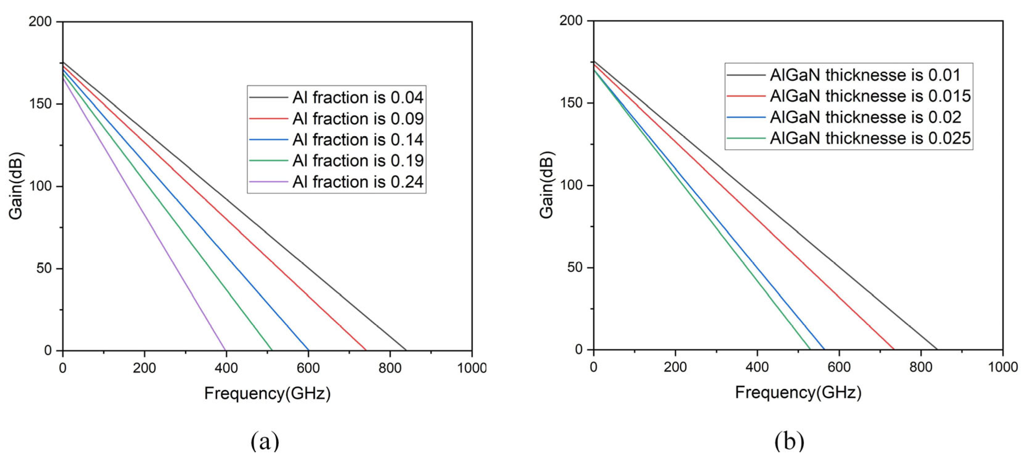
3.5. RF Characteristics

When defining a device’s frequency response characteristics, small signal parameters are crucial, especially the maximum oscillation frequency F m a x as well as the maximum cut-off frequency F t . Optimizing these parameters has turned out to be a great challenge for AlGaN/GaN HEMT devices for high-frequency applications. The frequency at which the unilateral power gain equals one is known as the maximum oscillation frequency, while the frequency at which the current gain equals zero is known as the maximum cut-off frequency. It is possible to compute the maximum cut-off frequency from Equation (8):
F t = g m 2 π C g s + C g d 1 + R s + R d R d s + g m C g d ( R s + R d )
where gm is the intrinsic transconductance, R s is the source resistor, R g is the gate resistor, C g s is the gate-source capacitance, R d s is the drain-source resistor, and C g d is the gate-drain capacitance.
The concentration of 2DEG is greater, the channel resistance is decreased, and the channel resistance between the drain and source is reduced in devices with additional AlGaN back barriers. At the same time, the AlGaN back-barrier layer becomes more confined to the 2DEG in the device, and the transconductance increases. Equation (8) shows that the cut-off frequency and transconductance are proportional; thus, the frequency characteristics are greatly improved. In addition, the symmetrical π-gate structure allows the reduction in parasitic capacitance to enhance the largest cut-off frequency. The π-gate structure exhibits a double-side contact pattern in the cross-section, which concentrates the electric field in the center of the channel rather than at the edges, reduces unnecessary gate-to-drain parasitic coupling, and thus significantly reduces the gate-drain capacitance and edge capacitance. Therefore, the largest cut-off frequency of the πGS structure is higher than that of the traditional t-gate structure. The introduction of the PN-junction field plate will substantially increase the gate capacitance and other parasitic capacitances in the device, lowering the maximum cut-off frequency compared to the conventional structure. The largest transconductance bias is used to evaluate the five structures’ RF characteristics. Figure 13a shows the cutoff frequency curves for five different structures. Around 839 GHz is the largest cut-off frequency of NπGS. The conventional t-gate structure has the largest cut-off frequency of around 653 GHz. In contrast to the conventional t-gate structure, the NπGS structure combines the advantages of a symmetric π-gate and an AlGaN back-barrier layer to improve the cut-off frequency by about 28%. Under high-frequency operating conditions, parasitic capacitance has a significant impact on device performance. A large Cgd amplifies the input equivalent capacitance through the Miller effect, which reduces the gain bandwidth product and limits the cut-off frequency. The edge capacitance also increases the total parasitic capacitance of the device, slowing down the charge response and thus reducing the cut-off frequency. And the gate capacitance of the NπGS is simulated to be around 63.8 fF/mm. The device has a very small total gate capacitance, indicating that the parasitic capacitance is well controlled. The new structure offers significant advantages in terms of frequency characteristics. The experimental results support the results derived from the following equation. The maximum oscillation frequency can be calculated from Equation (9) [42]:
F m a x = F t / 2 R i + R s + R g / R d s + 2 π F t R g C g d
where R s is the source resistor, R i is the internal resistor, R g is the gate resistor, R d s is the drain-source resistor, and C g d is the gate-drain capacitance.
The main factors affecting F m a x are F t and parasitic resistance. In general, the larger the cut-off frequency, the larger the oscillation frequency, and the smaller the parasitic resistance, the larger the oscillation frequency. The maximum oscillation frequency of NπGS is large; F m a x is about 168 GHz, as shown in Figure 13b. This also verifies that it has a larger cut-off frequency and smaller parasitic resistance. Figure 14a displays the NπGS structure’s maximum cut-off frequency curves for the AlGaN back-barrier layer with different Al fractions. As the Al component of the AlGaN back-barrier layer is larger, parasitic channels are created. The transconductance decreases, and the gate’s control over the two-dimensional electron gas is diminished when parasitic channels emerge. Therefore, the frequency capabilities of the device deteriorate significantly. Figure 14b shows the largest cut-off frequency curves of the NπGS structure with different thicknesses of the AlGaN back-barrier layer. When the thickness of the back-barrier layer increases, the frequency characteristics deteriorate. Because the greater thickness of the AlGaN back-barrier layer gradually puts the material interface in a relaxation state, the concentration of 2DEG in the main channel decreases. 2DEG is a key factor in determining the conductivity of the device, and a decrease in concentration means that the transconductance becomes smaller. At the same time, the parasitic channel is enhanced, and the leakage of the buffer layer rises when the thickness of the AlGaN back-barrier layer is thicker, which reduces the output resistance and increases the parasitic capacitance. The cut-off frequency is inversely proportional to the parasitic capacitance. The cut-off frequency is directly proportional to the transconductance. Eventually, the device’s cut-off frequency decreases, deteriorating the high-frequency response of the device. The best performance of the device is achieved when the thickness of the back-barrier layer is 0.01 μm and the Al fraction is 0.04.

4. Conclusions

In this paper, a new AlGaN/GaN high electron mobility transistor device with a π-gate (NπGS HEMT) is proposed. The NπGS HEMT, the traditional t-gate AlGaN/GaN HEMT, the BBS HEMT, the πGS HEMT, and the PN-JFPS HEMT are compared and analyzed with respect to various properties. These experimental findings demonstrate that the NπGS structure has improved both transfer characteristics, output characteristics, frequency characteristics, and voltage withstand characteristics, compared to the traditional t-gate structure. The NπGS structure has better DC characteristics, it achieves a transconductance of 336 mS· m m 1 and the maximum saturation drain current of 0.188 A/mm. The NπGS structure has a maximum oscillation frequency of 168 GHz and a maximum cut-off frequency of 839 GHz, which optimizes the frequency characteristics of traditional HEMT. For NπGS HEMT, the breakdown voltage reaches 1817 V, which is higher than that of the traditional structure. The new structure provides a new direction for the study of high voltage withstand and high RF in AlGaN/GaN HEMT devices. It has great potential for future applications in both the field of communication and power electronics.

Author Contributions

J.Y. contributed to the analysis, idea, paper writing, and measurements; D.Y. and C.L. assisted in the analysis and measurement; X.L. and W.Y. assisted in the work development, review, editing, and writing and contributed to the idea. All authors have read and agreed to the published version of the manuscript.

Funding

This study was supported by the National Natural Science Foundation of China (No. 41875026).

Data Availability Statement

Data and code are available from the corresponding authors upon reasonable request.

Conflicts of Interest

The authors declare no conflicts of interest.

References

  1. Mukherjee, K.; Darracq, F.; Curutchet, A.; Malbert, N.; Labat, N. TCAD simulation capabilities towards gate leakage current analysis of advanced AlGaN/GaN HEMT devices. Microelectron. Reliab. 2017, 76, 350–356. [Google Scholar] [CrossRef]
  2. Ghaffari, M.; Orouji, A.A. Dual trench AlGaN/GaN HEMT on SiC substrate: A novel device to improve the breakdown voltage and high power performance. Physica E 2016, 80, 108–114. [Google Scholar] [CrossRef]
  3. Sriramadasu, K.S.; Hsin, Y.-M. An AlGaN-GaN HEMT with p-GaN Extended Gate for Improvements on Current Dispersion and Breakdown Characteristics. ECS J. Solid State Sci. Technol. 2024, 13, 015004. [Google Scholar] [CrossRef]
  4. Li, J.; Yin, Y.; Zeng, N.; Liao, F.; Lian, M.; Zhang, X.; Zhang, K.; Zhang, Y.; Li, J. A dual-gate and Γ-type field plate GaN base E-HEMT with high breakdown voltage on simulation investigation. Semicond. Sci. Technol. 2021, 36, 095036. [Google Scholar] [CrossRef]
  5. Xu, K.; Wang, H.Y.; Chen, E.L.; Sun, S.X.; Wang, H.L.; Mei, H.Y. Improvement of DC and RF characteristics for a novel AlGaAs/InGaAs HEMT with decreased single event effect. J. Ovonic Res. 2024, 20, 395–403. [Google Scholar] [CrossRef]
  6. Lee, D.S.; Liu, Z.; Palacios, T. GaN high electron mobility transistors for sub-millimeter wave applications. Jpn. J. Appl. Phys. 2014, 53, 100212. [Google Scholar] [CrossRef]
  7. Wu, S.; Hao, Y.; Ma, X.; Yang, L.; Mi, M.; Zhang, M.; Wu, M.; Lu, Y.; Zhang, H.; Yi, C. A Millimeter-Wave AlGaN/GaN HEMT Fabricated With Transitional-Recessed-Gate Technology for High-Gain and High-Linearity Applications. IEEE Electron Device Lett. 2019, 40, 846–849. [Google Scholar] [CrossRef]
  8. Dubey, S.K.; Islam, A. Effect of high-k dielectric HfO2 on performance of AlGaN/GaN based MOSHEMT for RF applications. Microsyst. Technol. 2023, 30, 163–175. [Google Scholar] [CrossRef]
  9. Lu, Y.; Ma, X.; Yang, L.; Hou, B.; Mi, M.; Zhang, M.; Zheng, J.; Zhang, H.; Hao, Y. High RF Performance AlGaN/GaN HEMT Fabricated by Recess-Arrayed Ohmic Contact Technology. IEEE Electron Device Lett. 2018, 39, 811–814. [Google Scholar] [CrossRef]
  10. Kharei, P.; Baidya, A.; Maity, N.P.; Ghosh, A.; Zonunmawii, M. Novel double deck gate field plate structure on a normally-off AlGaN/GaN HEMT- An extensive analysis. Micro Nanostructures 2024, 192, 207874. [Google Scholar] [CrossRef]
  11. Meneghesso, G.; Meneghini, M.; Zanoni, E. Breakdown mechanisms in AlGaN/GaN HEMTs: An overview. Jpn. J. Appl. Phys. 2014, 53, 100211. [Google Scholar] [CrossRef]
  12. Peng, Z.; Liu, H.; Yu, H.; Li, L.; Chang, K.C. Constructing drain surrounded double gate structure in AlGaN/GaN HEMT for boosting breakdown voltage. RSC Adv. 2024, 14, 22238–22243. [Google Scholar] [CrossRef] [PubMed]
  13. Pal, P.; Pratap, Y.; Kabra, S. TCAD Simulation of Novel Recess Gate Common Drain Dual Channel AlGaN/GaN HEMT for Small Signal Performance. IETE Tech. Rev. 2024, 41, 621–631. [Google Scholar] [CrossRef]
  14. Lee, H.-J.; Lee, C.-C.; Pan, H.-R.; Kuan, C.-H. Optimization of Contact Resistance and DC Characteristics for AlGaN/GaN HEMTs Utilizing Sub-10 nm Nanohole Etching. Electronics 2024, 13, 2490. [Google Scholar] [CrossRef]
  15. Saito, W.; Takada, Y.; Kuraguchi, M.; Tsuda, K.; Omura, I.; Ogura, T.; Ohashi, H. High breakdown voltage AlGaN-GaN power-HEMT design and high current density switching behavior. IEEE Trans. Electron Devices 2003, 50, 2528–2531. [Google Scholar] [CrossRef]
  16. Dora, Y.; Chakraborty, A.; McCarthy, L.; Keller, S.; Denbaars, S.P.; Mishra, U.K. High Breakdown Voltage Achieved on AlGaN/GaN HEMTs With Integrated Slant Field Plates. IEEE Electron Device Lett. 2006, 27, 713–715. [Google Scholar] [CrossRef]
  17. Wen, Z.; Xu, Y.; Chen, Y.; Tao, H.; Ren, C.; Lu, H.; Wang, Z.; Zheng, W.; Zhang, B.; Chen, T.; et al. A Quasi-Physical Compact Large-Signal Model for AlGaN/GaN HEMTs. IEEE Trans. Microw. Theory Tech. 2017, 65, 5113–5122. [Google Scholar] [CrossRef]
  18. Qu, A.; Xie, Z.; Wang, Y.; Hu, G.; Tan, C.-K. Effect of Acceptor-Type Traps in GaN Buffer Layer on Current Collapse of ε-Ga2O3/GaN HEMTs. J. Electron. Mater. 2025, 54, 3086–3096. [Google Scholar] [CrossRef]
  19. Du, J.; Liu, D.; Bai, Z.; Liu, Y.; Yu, Q. Design of high breakdown voltage GaN-based vertical HFETs with p-GaN island structure for power applications. Superlattices Microstruct. 2015, 85, 690–696. [Google Scholar] [CrossRef]
  20. Wang, H.; Wei, J.; Xie, R.; Liu, C.; Tang, G.; Chen, K.J. Maximizing the Performance of 650-V p-GaN Gate HEMTs: Dynamic RON Characterization and Circuit Design Considerations. IEEE Trans. Power Electron. 2017, 32, 5539–5549. [Google Scholar] [CrossRef]
  21. Yu, Q.; Shi, C.; Yang, L.; Lu, H.; Zhang, M.; Zou, X.; Wu, M.; Hou, B.; Gao, W.; Wu, S.; et al. Improved DC and RF Characteristics of GaN-Based Double-Channel HEMTs by Ultra-Thin AlN Back Barrier Layer. Micromachines 2024, 15, 1220. [Google Scholar] [CrossRef] [PubMed]
  22. Natarajan, R.; Murugapandiyan, P.; Vigneshwari, N.; Mohanbabu, A.; Ravi, S. Investigation of different buffer layer impact on AlN/GaN/AlGaN HEMT using silicon carbide substrate for high-speed RF applications. Micro Nanostructures 2024, 189, 207815. [Google Scholar] [CrossRef]
  23. Sun, S.; Zhang, Y.; Si, Y.; Xiong, J.; Luo, X. Improvement of Breakdown Characteristic for a Novel GaN HEMT with Enhanced Resistance Single-Event Transient Effect. J. Electron. Mater. 2024, 54, 784–791. [Google Scholar] [CrossRef]
  24. Uren, M.J.; Moreke, J.; Kuball, M. Buffer Design to Minimize Current Collapse in GaN/AlGaN HFETs. IEEE Trans. Electron Devices 2012, 59, 3327–3333. [Google Scholar] [CrossRef]
  25. Liu, Y.; Yu, Q.; Du, J. Simulation design of a high-breakdown-voltage p-GaN-gate GaN HEMT with a hybrid AlGaN buffer layer for power electronics applications. J. Comput. Electron. 2020, 19, 1527–1537. [Google Scholar] [CrossRef]
  26. Xing, H.; Dora, Y.; Chini, A.; Heikman, S.; Keller, S.; Mishra, U.K. High Breakdown Voltage AlGaN–GaN HEMTs Achieved by Multiple Field Plates. IEEE Electron Device Lett. 2004, 25, 161–163. [Google Scholar] [CrossRef]
  27. Tsatsulnikov, A.F.; Lundin, V.W.; Zavarin, E.E.; Yagovkina, M.A.; Sakharov, A.V.; Usov, S.O.; Zemlyakov, V.E.; Egorkin, V.I.; Bulashevich, K.A.; Karpov, S.Y.; et al. effect of the parameters of AlN/GaN/AlGaN and AlN/GaN/InAlN heterostructures with a two-dimensional electron gas on their electrical properties and the characteristics of transistors on their basis. Semiconductors 2016, 50, 1383–1389. [Google Scholar] [CrossRef]
  28. Neha; Kumari, V.; Gupta, M.; Saxena, M. TCAD-Based Optimization of Field Plate Length & Passivation Layer of AlGaN/GaN HEMT for Higher Cut-Off Frequency & Breakdown Voltage. IETE Tech. Rev. 2020, 39, 63–71. [Google Scholar] [CrossRef]
  29. Yu, H.; Lisesivdin, S.B.; Bolukbas, B.; Kelekci, O.; Ozturk, M.K.; Ozcelik, S.; Caliskan, D.; Ozturk, M.; Cakmak, H.; Demirel, P.; et al. Improvement of breakdown characteristics in AlGaN/GaN/AlxGa1−xN HEMT based on a grading AlxGa1−xN buffer layer. Phys. Status Solidi A 2010, 207, 2593–2596. [Google Scholar] [CrossRef]
  30. Hanawa, H.; Horio, K. Increase in breakdown voltage of AlGaN/GaN HEMTs with a high-k dielectric layer. Phys. Status Solidi A 2014, 211, 784–787. [Google Scholar] [CrossRef]
  31. Jiang, Y.; Du, F.; Wang, P.; He, J.; Wen, K.; Deng, C.; Zhang, Y.; Li, M.; Wang, X.; Wang, Z.; et al. Gate Leakage suppression and breakdown improvement of InAlN/GaN MIS-HEMTs with N2O surface treatment. J. Alloys Compd. 2025, 1024, 179922. [Google Scholar] [CrossRef]
  32. Cheng, J.; Wang, Q.; Liu, Y.; Ding, G.; Zhang, M.; Yi, B.; Huang, H.; Yang, H. Study on a p-GaN HEMT with composite passivation and composite barrier layers. Semicond. Sci. Technol. 2024, 39, 085004. [Google Scholar] [CrossRef]
  33. Langpoklakpam, C.; Hsiao, Y.-K.; Yi Chang, E.; Lin, C.-H.; Kuo, H.-C. Analysis of breakdown voltage for GaN MIS-HEMT with various composite field plate configurations and passivation layers. Solid-State Electron. 2024, 216, 108930. [Google Scholar] [CrossRef]
  34. Cui, A.; Zhang, J.; Ren, Z.; Zhou, H.; Wang, D.; Wu, Y.; Lei, Y.; Zhang, J.; Hao, Y. Microwave power performance analysis of hydrogen terminated diamond MOSFET. Diam. Relat. Mater. 2021, 118, 108538. [Google Scholar] [CrossRef]
  35. Sun, H.; Liu, M.; Liu, P.; Lin, X.; Cui, X.; Chen, J.; Chen, D. Performance optimization of lateral AlGaN/GaN HEMTs with cap gate on 150-mm silicon substrate. Solid-State Electron. 2017, 130, 28–32. [Google Scholar] [CrossRef]
  36. Luo, S.; Liu, X.; Jiang, X. Effect of Source–Drain Opposite Side Gate on the AlGaN/GaN High Electron Mobility Transistor Devices. Phys. Status Solidi A 2023, 220, 2300375. [Google Scholar] [CrossRef]
  37. Wang, P.; Deng, C.; Cheng, H.; Cheng, W.; Du, F.; Tang, C.; Geng, C.; Tao, N.; Wang, Q.; Yu, H. Simulation of High Breakdown Voltage, Improved Current Collapse Suppression, and Enhanced Frequency Response AlGaN/GaN HEMT Using A Double Floating Field Plate. Crystals 2023, 13, 110. [Google Scholar] [CrossRef]
  38. Li, M.; Zhao, Z.B.; Fan, L.B. Effect of spin-orbit coupling on the wave vector and spin dependent transmission probability for the GaN/AlGaN/GaN heterostructure. Phys. Scr. 2015, 90, 015806. [Google Scholar] [CrossRef]
  39. Wang, W.K.; Li, Y.J.; Lin, C.K.; Chan, Y.J.; Chen, G.T.; Chyi, J.I. Low Damage, Cl2-Based Gate Recess Etching for 0.3-μm Gate-Length AlGaN/GaN HEMT Fabrication. IEEE Electron Device Lett. 2004, 25, 52–54. [Google Scholar] [CrossRef]
  40. Niu, D.; Wang, Q.; Li, W.; Chen, C.; Xu, J.; Jiang, L.; Feng, C.; Xiao, H.; Wang, Q.; Xu, X.; et al. Hybrid-gate structure designed for high-performance normally-off p-GaN high-electron-mobility transistor. Jpn. J. Appl. Phys. 2020, 59, 111001. [Google Scholar] [CrossRef]
  41. Jebalin, I.B.K.; Franklin, S.A.; Nirmal, D. Revolutionizing Fe doped back barrier AlGaN/GaN HEMTs: Unveiling the remarkable 1700V breakdown voltage milestone. Microelectron. J. 2024, 147, 106158. [Google Scholar] [CrossRef]
  42. Chung, J.W.; Hoke, W.E.; Chumbes, E.M.; Palacios, T. AlGaN/GaN HEMT With 300-GHz fmax. IEEE Electron Device Lett. 2010, 31, 195–197. [Google Scholar] [CrossRef]
Figure 1. Schematic of the new π-gate AlGaN/GaN HEMT structure.
Electronics 14 02947 g001
Figure 2. Two-dimensional interface diagram: (a) The traditional t-gate structure. (b) The back-barrier AlGaN/GaN HEMT structure. (c) The πGS structure. (d) The PN-JFPS structure. (e) The NπGS structure.
Electronics 14 02947 g002
Figure 3. Electron concentration: (a) The traditional t-gate structure in the on-state. (b) The NπGS structure in the on-state.
Electronics 14 02947 g003
Figure 4. Energy band diagrams of the traditional t-gate structure and NπGS structure in the on-state.
Electronics 14 02947 g004
Figure 5. (a) Transfer characteristic curves of two different structures. (b) Transconductance curves of two different structures.
Electronics 14 02947 g005
Figure 6. Heterojunction energy band variation diagram: (a) Energy band diagram when V g = 0 . (b) Energy band diagram when V g < 0 . (c) Energy band diagram when V g > 0 .
Electronics 14 02947 g006
Figure 7. Transconductance curves: (a) The NπGS structure under the AlGaN back-barrier layers with different Al fractions. (b) The NπGS structure under different thicknesses of the AlGaN back-barrier layer.
Electronics 14 02947 g007
Figure 8. Output characteristic curves: (a) Four different structures. (b) The NπGS structure under the AlGaN back-barrier layer with different Al fractions. (c) The NπGS structure under different thicknesses of the AlGaN back-barrier layer.
Electronics 14 02947 g008
Figure 9. Major breakdown mechanisms in GaN HEMT.
Electronics 14 02947 g009
Figure 10. Before device breakdown: (a) Electric field diagram below the gate of NπGS. (b) Two-dimensional electric field contour plots for NπGS.
Electronics 14 02947 g010
Figure 11. After device breakdown: (a) Electric field diagram below the gate of NπGS. (b) Two-dimensional electric field contour plots for NπGS.
Electronics 14 02947 g011
Figure 12. (a) Breakdown voltage curves for four different structures. (b) Breakdown voltage curves of the NDGS structure for different gate-drain distances.
Electronics 14 02947 g012
Figure 13. (a) Cut-off frequency curves under five different structures. (b) Oscillation frequency curves under five different structures.
Electronics 14 02947 g013
Figure 14. Cut-off frequency curves: (a) The NπGS structure under the AlGaN back-barrier layer with different Al fractions. (b) The NπGS structure under the AlGaN back-barrier layer with different thicknesses.
Electronics 14 02947 g014
Table 1. The 2D cross-sectional dimensions of the structure.
Parameter NameValueUnit
Source length/height 0.5/0.12μm
Drain length/height0.5/0.12μm
Gate length1.5/0.25μm
Gate height0.03/0.03μm
gap between the two pillars0.14μm
distance from Gate to Drain3.9μm
AlGaN layer length/height7.3/0.022μm
GaN layer length/height7.3/0.048μm
AlGaN back-barrier layer length/height7.3/0.01μm
PN-junction field plate length/height0.5/0.01μm
Table 2. Performance comparison of NπGS with representative GaN HEMTs in recent years.
Structure TypeBv (V)Fₜ (GHz)Year
NπGS 18178342025
ITGS-DOSS16616252023
two-step D-FP with G-FP1700/2024
Gate field plate15904002017
Gate field plate with Diamond substrate2000902021
Disclaimer/Publisher’s Note: The statements, opinions and data contained in all publications are solely those of the individual author(s) and contributor(s) and not of MDPI and/or the editor(s). MDPI and/or the editor(s) disclaim responsibility for any injury to people or property resulting from any ideas, methods, instructions or products referred to in the content.

