1. Introduction
With the rapid advancement of high-performance artificial intelligence (AI) and high-performance computing (HPC), there is an increasing demand for ultra-high-speed, high-capacity memory capable of processing large volumes of data efficiently. Conventional 2D-DRAM faces limitations in the chip integration density and data transfer speed, making it inadequate to meet the demands of AI and HPC applications [
1].
High-Bandwidth Memory (HBM) adopts a three-dimensional (3D) stacking approach by vertically stacking multiple memory dies and minimizing the distance between the logic die and memory dies through a silicon interposer. This structure enables both a high integration density and high bandwidth, offering significantly improved data transfer efficiency compared to conventional DRAM within the same area, making it highly suitable for large-scale computational tasks [
2].
As the computational workload required for HPC and AI applications continues to increase rapidly, the power density within semiconductor chips rises accordingly, leading to a substantial increase in heat generation. Since the power consumed by a chip is ultimately converted into heat, the greater the data processing workload, the more heat is generated within the chip [
3]. If this heat is not effectively dissipated, the junction temperature rises, resulting in reduced operational speed or even potential device failure.
High-density, high-performance devices dissipate large amounts of heat because every fundamental power component grows unfavorably as integration and clock speed rise. The three dominant contributors can be expressed separately as Equations (1)–(3).
where
Modern HPC cores push the clock frequency
into the multi-gigahertz range and widen datapaths, so the product
rises and
, the dynamic power, which is expressed as in the definition in Equation (1), dominates [
4]. Process scaling lowers threshold voltages and increases the leakage current
, raising the
which is expressed as in the definition in Equation (2) [
5]. In addition, an HBM stack that drives thousands of TSV-fed I/O lines at multi-gigabit speeds injects extra
heat into micro-bumps and redistribution layers (Equation (3)). When these power sources are confined to a compact 3D stack, their cumulative effect makes thermal management a first-order design constraint.
The primary challenge lies in the fact that HBM’s 3D stacked structure complicates the heat dissipation pathway. Because HBM stacks multiple memory dies vertically, the heat generated within the dies must travel through various interfaces, such as Through-Silicon Vias (TSVs) and underfill layers, before reaching either the lower or upper dies. This process leads to heat accumulation within the stack, exacerbating localized overheating, which ultimately degrades the memory performance and reduces its lifespan [
6,
7,
8,
9].
Other failures in electronic components are caused by thermal stress in approximately 55% of cases [
10]. In stacked memory, issues arising from mismatched coefficients of thermal expansion (CTE) have become just as critical as thermal problems. Because multiple materials (silicon, copper, and dielectric layers) are stacked in a 3D structure, each layer has a different CTE. As a result, a variety of reliability concerns may emerge, which are presented on
Table 1.
High-temperature, high-pressure TCB increases residual stress and warpage, whereas low-temperature, thin-interface hybrid bonding suppresses inter-layer stress and prevents Cu protrusion [
14,
15].
In
Section 2 of the main body of this paper, the thermal characteristics of 3D stacked memory are analyzed, addressing key issues such as limitations in heat conduction pathways, the impact of TSV and underfill structures, and increased heat accumulation according to the stack height.
In addition, potential solutions are discussed from material and design perspectives, including material selection and structure design considering heat dissipation. Subsequently, the thermal performance differences between TCB and hybrid bonding methods are compared, and an analysis is conducted on how hybrid bonding forms efficient heat-dissipation pathways and enables more stable thermal management in high-density memory structures. Finally, specific design strategies for improving the thermal performance of hybrid bonding are proposed.
In
Section 3 of the main body, the major issues caused by CTE mismatch are examined in detail, and various potential solutions are discussed from different perspectives, including thermal process control, Chemical Mechanical Polishing (CMP), and package design. Through this analysis, the advantages of hybrid bonding over conventional TCB methods are explored, and this study aims to seek stable process directions necessary for advancing 3D stacked memory into higher-layer configurations.
2. Background and Research Approaches in Hybrid Bonding
2.1. Research Gaps and Objectives
While several recent reviews have addressed various aspects of thermal management in 3D ICs and High-Bandwidth Memory (HBM), there remain critical research gaps that this paper explicitly seeks to address. Based on an analysis of the existing literature, we have identified four primary shortcomings in prior studies:
Firstly, most previous reviews are limited to evaluating thermal characteristics and reliability within 8–12-layer stack configurations, despite the industry’s rapid shift toward ultra-high-stack structures exceeding 16 layers. Reviews primarily focus on relatively lower-layer test vehicles. Our review specifically extends the quantitative analysis to stacks of 16 layers and beyond, assessing thermal resistance, mechanical stresses induced by coefficient of thermal expansion (CTE) mismatch, and electrical performance impacts comprehensively [
16,
17].
Secondly, the existing literature predominantly emphasizes thermal resistance reduction alone, without adequately considering the interplay between thermal management and electrical performance. Reviews do not analyze how optimizations for heat dissipation affect the signal integrity, I/O delay, or power consumption. To bridge this gap, our paper quantitatively examines these tradeoffs, presenting a multi-dimensional framework that incorporates thermal resistance, mechanical reliability (CTE-induced stress), and electrical performance criteria [
16,
18,
19].
Thirdly, prior studies often overlook quantitative analyses of thermo-mechanical stress and defect mechanisms arising from CTE mismatches [
20].
Finally, previous research has largely presented TSV arrangement and package structural optimization strategies qualitatively or conceptually, without providing specific numerical guidelines [
16].
Based on these identified gaps, this review sets clear objectives:
To quantitatively analyze thermal, mechanical, and electrical performance in ultra-high-stack HBM structures.
To explicitly map and integrate the interdependencies and trade-offs among thermal resistance, mechanical stress, and electrical performance.
To provide practical, numerically supported multi-dimensional guidelines involving advanced dielectrics (SiCN), optimized low-temperature hybrid bonding processes (under 200 °C), and effective structural designs to simultaneously enhance thermal management, mechanical reliability, and electrical performance in high-layer-count HBM systems.
2.2. Limitations of External Cooling
As shown in
Figure 1 and
Figure 2, the 3D stacked structure restricts heat dissipation pathways between dies, while internal components such as TSVs and underfill accelerate heat accumulation, leading to localized overheating and performance degradation. To mitigate this issue, external cooling methods can be considered an initial solution. Various external cooling techniques, including heat spreaders, microchannel, heatsinks, and Through Mold Plate (TMP), have been explored to rapidly dissipate the heat generated in the stacked structure to the exterior of the package [
18,
21,
22]. TMP, in particular, is positioned between the GPU and HBM to minimize thermal coupling and effectively transfer heat to the heatsink.
One study has demonstrated that TMP can reduce the HBM junction temperature by approximately 10.3 °C and decrease signal jitter by up to 4.54% [
25]. However, external cooling methods have inherent limitations as they do not fundamentally address internal heat accumulation within the 3D stacked structure or around TSVs [
26]. As illustrated in
Figure 1, the issue of internal heat buildup becomes more severe when the HBM stack height increases (beyond 12 layers). Additionally, enlarging cooling devices result in increased size and power consumption, which can hinder the development of high-performance compact devices. Consequently, external cooling alone is insufficient to fully control internal thermal resistance, making it crucial to focus on bonding optimization within the structure [
27].
2.3. Importance of Internal Bonding Technology
As shown in
Figure 3a, the earliest semiconductor interconnect technology employed wire bonding, followed by the flip-chip bonding illustrated in
Figure 3b; subsequent advances include micro-bump bonding and, most recently, hybrid bonding, which directly connects copper-to-copper (Cu–Cu) or copper-to-dielectric (Cu–SiO
2) interfaces. Wire bonding is a simple and cost-effective method; however, it has limitations in the connection density and signal delay, leading to the development of Thermo-Compression Non-Conductive Film (TC-NCF) and Mass Reflow–Molded Underfill (MR-MUF) technologies, which utilize flip-chip and micro-bumps [
28]. While these approaches have enhanced the reliability of electrical connections and the stacking density, they have not fully addressed the challenge of heat-dissipation pathways. To overcome this limitation, hybrid bonding has emerged as a promising solution, particularly in HBM stacked structures, as it improves both the electrical connectivity and thermal dissipation. The evolution of bonding technologies can be seen in
Figure 4.
As shown in
Figure 5, TC-NCF forms physical and electrical connections between dies by bonding metal bumps and underfill materials under high-temperature and pressure conditions. By precisely adjusting the metal density and bonding height, this technique can significantly reduce interfacial thermal resistance. MR-MUF, as illustrated in
Figure 6, injects a composite underfill material containing high-thermal-conductivity fillers rather than using underfill solely as a gap-filling material. Direct Bond Interconnect (DBI) utilizes Cu–Cu direct bonding, creating an ultra-thin and dense bonding interface, thereby shortening the heat dissipation path. Hybrid bonding, which simultaneously bonds copper and dielectric materials (such as polymers and SiO
2), is gaining attention as a promising alternative that enhances both electrical and thermal performance.
Oprins et al. [
32] experimentally analyzed the effect of TSV density on heat dissipation in 3D-stacked ICs, testing three cases: no TSVs, a 7 × 7 TSV array (5% density), and an 11 × 11 TSV array (12% density). While TSVs were expected to enhance heat dissipation, the 7 × 7 array unexpectedly increased the hotspot temperature due to non-uniform adhesive distribution around TSVs. In contrast, the 11 × 11 array (12% density) reduced the hotspot peak temperature by ~20%, as a higher TSV density facilitated effective heat transfer to the bottom die. The study concluded that heat dissipation improves significantly only with a sufficiently high TSV density, while a low density may have minimal or adverse effects.
Kikuchi et al. [
33] conducted a study to analyze the thermal characteristics of the Back-End-of-Line (BEOL) layer to improve the thermal resistance of 3D-stacked memory. In the study, a sample with a Face-to-Face (F2F) stacking structure was fabricated. This structure does not include a TSV. In the cooling performance analysis using Cu pillar thermal bumps, reducing the bump pitch from 100 µm to 50 µm lowered the maximum chip temperature by 12 °C. Additionally, selectively placing denser thermal bumps in hotspot regions further reduced the temperature by 3 °C.
Kim et al. [
34] conducted a study focusing on thermal management optimization in TC-NCF bonding by adjusting the metal density, dielectric thermal conductivity, and bonding height. The study found that increasing the metal density above 30% significantly reduced the thermal resistance, as the majority of heat flow was conducted through the metal regions.
Additionally, reducing the bonding height by half and doubling the thermal conductivity of the dielectric resulted in 37% and 6% reductions in thermal resistance, respectively. However, the bonding height also affects the mechanical stability, necessitating the exploration of alternative approaches.
Recently, the MR-MUF method has gained attention for its ability to enhance heat dissipation between the memory chip and the substrate by using high-thermal-conductivity materials. Lee et al. [
28] compared MR-MUF bonding with TC-NCF bonding, which utilizes non-conductive films. The results showed that under the same DRAM operating conditions, the maximum junction temperature of memory chips using MR-MUF was reduced by 14 °C, indicating that this approach can significantly mitigate thermal management issues in HBM.
Originally, TSVs are designed to provide electrical connections between dies, as seen in
Figure 7. Studies have also been conducted focusing on TSV placement for thermal management. A thermal resistance network model was used to simulate the temperature distribution in overheating regions of 3D integrated circuits (3D-ICs). A solution was proposed to insert thermal TSVs (TTSVs) to address excessive heat buildup. Thermal TSVs provided a vertical heat dissipation path from overheated regions, significantly lowering temperatures and improving the overall thermal management performance [
35,
36].
Furthermore, Wang at al. [
37] compared 4 × 4 and 6 × 6 TSV arrays, demonstrating that the 6 × 6 TSV array met the thermal requirements of a peak temperature of 315 K and an average temperature of 310 K. The study confirmed that optimizing TSV arrangements can achieve a more uniform thermal distribution. The difference between the 4 × 4 and 6 × 6 configurations can be observed in
Figure 8.
Another area of research explored Direct Bond Interconnect (DBI), which involves first bonding the dielectric layer and then directly bonding Cu–Cu connections. This method creates thinner interfaces compared to TSVs, thereby shortening internal heat-dissipation pathways. Agrawal at al. [
38] investigated the application of DBI in an 8-die HBM stack, revealing that compared to thermo-compression bonding, DBI reduced the junction temperature by approximately 26% while significantly decreasing temperature fluctuations, leading to enhanced thermal stability. Ultimately, these internal bonding techniques provide efficient heat-dissipation pathways within the stacked structure. These findings are summarized in
Table 2. As the number of stacked layers increases, the risk of heat accumulation also rises.
However, by optimizing the metal density, interface thickness, and underfill composition, localized overheating can be suppressed, allowing high-layer HBM stacks to maintain a stable temperature distribution.
As HBM technology advances, power consumption is also increasing. Although the absolute power consumption of HBM is lower than that of GPUs, further developments may lead to a scenario where the power density of HBM PHY (the physical layer transceiver circuitry that handles high-speed data transfer between the memory stacks and controller) surpasses that of GPUs. Therefore, thermal management should be considered not only for GPUs but also for HBM. The increasing power consumption within HBM–GPU modules reinforces the importance of research focused on internal thermal management in HBM [
39].
2.4. High-Thermal-Conductivity Composite Underfills
Recent advances demonstrate that the thermal bottleneck of polymeric underfills can be lifted not by exotic chemistries but by engineering how conventional ceramic fillers occupy, interconnect, and orient themselves inside the resin.
Gao et al. [
40] showed that a 3D network in a network concept works. Replacing neat epoxy with a 50 wt % blend of silane functionalized h-BN (hexagonal Boron Nitride) platelets and α-Al
2O
3 nanoparticles raised the through plane conductivity to 0.85 W m
−1 K
−1, four times higher than the matrix and 10% higher than the same blend without surface treatment, proving that covalent bridging across the filler polymer interface is already worth a double digit gain.
Building on this hybrid-filler logic, Lee Sánchez et al. [
41] loaded an epoxy with 80 wt % of a spherical Al
2O
3/flake-BN mixture (7: 1 by mass) and achieved 1.72 W m
−1 K
−1, an almost eight times jump over the pristine resin and 15% better than an Al
2O
3-only control, because two dimensional BN flakes span the gaps left between zero dimensional spheres to complete a percolated pathway.
Replacing Al
2O
3 with higher-thermal-conductivity AlN while keeping the BN bridge intact pushed the limit even further: at 75 wt % total filler, the composite reached 10.18 W m
−1 K
−1, 49% above the AlN only analogue and 46 times higher than that of the neat epoxy, yet it remained processable because the BN content was capped before viscosity became prohibitive [
42].
Whereas these three studies rely on composition and inter-particle packing to create isotropic 3D networks, Hong et al. [
43] demonstrated that geometric alignment offers a complementary lever, as coating h-BN platelets with Fe
3O
4, dispersing them to 40 vol %, and magnetically orienting the flakes perpendicular to the chip plane produced an anisotropic underfill for which the through plane conductivity soared to 5.77 W m
−1 K
−1, which is 162% higher than its randomly oriented counterpart, while the in-plane value remained modest (2.25 W m
−1 K
−1).
Taken together, these four studies outline a clear design strategy for next-generation HBM underfills. First, mixing fillers with complementary shapes and thermal conductivities helps close percolation gaps. Second, enhancing phonon coupling at the polymer–filler interface through tailored surface chemistry improves heat transfer. Third, applying anisotropic alignment is effective when directional heat removal is required. Fourth, filler loading must be carefully balanced with the rheological behavior and dielectric constraints. When integrated with thin-gap hybrid bonding processes, these approaches can reduce interfacial thermal resistance and improve heat dissipation without compromising the mechanical compliance or processing temperatures.
2.5. Hybrid Bonding Process and Advantages over TCB
Hybrid bonding simultaneously integrates copper (Cu) and dielectric materials, leveraging copper’s high thermal conductivity (approximately 390 W/m × K) while using dielectrics to reduce signal interference and stabilize electrical properties. Notably, hybrid bonding allows for fine-pitch bonding below 10 µm, achieving a higher integration density and superior thermal and electrical performance compared to TSVs or micro-bumps.
Figure 9 illustrates the hybrid bonding process for 3D-stacked memory, where copper (Cu) and dielectric materials are bonded together, enhancing signal isolation and circuit design flexibility, further improving the overall system performance. The process includes eight steps: (a) chip fabrication with an SiO
2 layer on a silicon substrate, (b) SiO
2 dry etching to create trenches, (c) Cu electroplating to fill trenches with copper, (d) Cu/SiO
2 CMP for surface planarization, (e) plasma treatment to clean and activate the surface, (f) covalent bonding of SiO
2 surfaces between two chips, (g) annealing to enhance Cu–Cu bonding and manage thermal expansion, and (h) final Cu–SiO
2 bonding, achieving a high-density, low-resistance interface with improved thermal conductivity (e.g., 0.8 mm
2 × K/W) and electrical performance, though challenges like CTE mismatch and process precision remain critical for scalability in HBM applications [
44].
Figure 10 illustrates the hybrid bonding interface in 3D-stacked memory, where copper (Cu) and dielectric materials form direct connections between two surfaces, enhancing signal isolation and circuit design flexibility, thereby improving the overall system performance. The cross-sectional view shows Cu pads (brown) embedded in a dielectric (gray) on silicon substrates, with Cu–Cu bonds providing low thermal resistance and high electrical conductivity, while dielectric–dielectric bonds ensure mechanical stability and isolation, though challenges like CTE mismatch and process precision remain critical for scalability in high-layer HBM stacks [
45].
Oprins et al. [
45] compared the thermal resistance of hybrid Cu/dielectric wafer-to-wafer (W2W) bonding with conventional micro-bump (µbump) stacking. Using 300 mm test wafers and passive test chip (PTCS) structures, they found that the hybrid bonding interface had a thermal resistance of 1.2 mm
2 × K/W—significantly lower than the 4.2 mm
2 × K/W of µbump stacking (40 µm pitch, 13 µm standoff). The thinner bonding layer (1.3 µm) in hybrid bonding reduces the standoff height, improving thermal conductivity. This makes hybrid bonding a superior thermal management solution for high-density 3D ICs. Oprins et al. [
46] measured the thermal resistance of hybrid Cu/dielectric bonding at 1.2 mm
2 × K/W—four times lower than micro-bumps (8–19 mm
2 × K/W) and twice as low as Cu–Cu bonding with a BCB adhesive. The bonding layer thickness was reduced from 16 μm to 1.3 μm, significantly improving thermal conductivity. This feature makes hybrid bonding highly suitable for thermally demanding applications such as high-density 3D stacking in HBM and advanced packaging.
Cherman et al. [
47] applied Cu–Cu hybrid bonding with a 2.5 μm pitch to assess the thermal resistance of a metal-to-metal bonded interface. The experimental results showed that the thermal resistance of the hybrid bonding interface decreased to 0.8 mm
2 × K/W, which was 0.4 mm
2 × K/W lower than the value reported in Oprins et al. [
45]. Post-bond annealing was performed at 250 °C for 2 h, improving the bonding quality and reducing voids in the bonding interface, leading to further reductions in thermal resistance. Additionally, the study incorporated the effects of the Back End of Line (BEOL) layer, ensuring a more accurate assessment of thermal dissipation performance in real semiconductor packaging environments.
In the study by Nigussie et al. [
48], hybrid bonding (HyB) demonstrated superior thermal performance compared to thermo-compression bonding (TCB). In the case of TCB, the temperature difference (T
FEOLmax–T
FEOLmin) was measured at 8.01 °C, indicating that high bonding resistance makes heat dissipation difficult, leading to an increase in the internal temperature. In contrast, HyB exhibited a lower temperature difference of 5.42 °C, as its high bonding density allows for more uniform heat distribution. Additionally, HyB reduced the wire length by up to 57% compared to TCB, decreased logic and total power consumption by up to 34% and 22%, respectively, and achieved an 11% reduction in the silicon area.
Kim et al. [
49] demonstrated that HBM with hybrid bonding (HyB) reduces thermal resistance by 22.8% compared to micro-bump-based HBM. Additionally, HyB reduces the total stack height by more than 15%, minimizing heat accumulation. Their analysis of an 8-Hi HBM showed that HyB improves vertical heat transfer by replacing micro-bumps and underfill with Cu/Cu direct bonding, while optimized passivation layers enhance heat dissipation. This makes HyB a superior solution for thermal management in high-density memory stacks.
Thermal simulation results from Mehta et al. [
14] demonstrated that hybrid bonding in 16-Hi HBM structures achieves approximately 47% lower thermal resistance compared to microbumps, attributed to the continuous thermal conduction path enabled by Cu–Cu direct bonding. While hybrid bonding has proven thermally superior in multi-layer stacking environments, the systematic optimization of design parameters such as the copper layer thickness, metal density, and bonding height becomes critical to address heat accumulation issues in high-stack HBMs exceeding 12 layers. This study quantitatively analyzes how these key factors influence thermal resistance improvements, aiming to develop design strategies that optimize internal heat-transfer pathways that cannot be sufficiently addressed by external cooling alone.
2.6. Research Advances and Methodologies in Hybrid Bonding Technology
This section systematically analyzes research methodologies for evaluating hybrid bonding thermal performance, focusing on experimental measurements (temperature sensors/heaters) and computational simulations (MD/FEM). Studies typically investigate key variables including the Cu pad geometry (density, diameter, pitch), interface materials, crystallographic orientation, and contact pressure while measuring the thermal conductivity (W/m × K), interfacial heat transfer coefficient (MW/m2K), and temperature distribution.
The analysis classifies thermal optimization strategies into three main research perspectives. First, the metal pad layout and overall metal density are examined for their influence on heat conduction. Second, material selection and interface characteristics are considered, with an emphasis on enhancing thermal coupling. Third, mechanical and structural design approaches are evaluated for their role in managing interfacial heat flow. While some studies also address electrical performance, this review specifically focuses on thermal metrics and their quantitative improvements across different experimental and modeling efforts.
2.6.1. Metal Pad Design and Metal Density
Oprins et al. [
50] evaluated the impact of the bonding interface on thermal resistance in 3D wafer-to-wafer (W2W) hybrid Cu/dielectric bonding. The results, as shown in
Figure 11, indicate that an interface without any Cu pads exhibited the highest thermal resistance.
When Cu pads were introduced with a 1.35 µm pitch and 17% Cu density, the thermal resistance was reduced by 26%. Increasing the pitch to 1.75 µm and the Cu density to 22% resulted in a total reduction of approximately 38%. These results are summarized in
Table 3. The study attributed this reduction to the increase in metallic heat conduction pathways bypassing the dielectric, which significantly improved interfacial heat transfer. The study provides experimental evidence that the Cu pad density critically influences the thermal resistance of the bonding interface.
Han et al. [
51] systematically investigated thermal conductivity optimization in Chip-to-Wafer (C2W) hybrid bonding through three distinct Cu pad configurations (
Figure 12).
Group 1 (3 µm diameter, 6 µm pitch, 17 × 17 array), as shown in
Figure 12a, represented high-density packaging; Group 2 (3 µm diameter, 10 µm pitch, 10 × 10 array), as shown in
Figure 12b, demonstrated intermediate density; and Group 3 (5 µm diameter, 10 µm pitch, 10 × 10 array), as shown in
Figure 12c, shows how an increased pad size affects the thermal performance. The study revealed that while Group 1 and Group 3 had similar Cu coverage percentages, their thermal characteristics differed significantly due to pitch variation, as the tighter 6 µm pitch in Group 1 created more continuous heat-transfer pathways despite smaller individual pads. Group 2′s lower density configuration served as a control, highlighting how reduced Cu content increases the thermal resistance. These findings demonstrate that thermal management in hybrid bonding requires the simultaneous optimization of three key geometric parameters: pad diameter (directly affecting contact area), pitch (determining heat path density), and array pattern (influencing thermal flow uniformity). The research provides a quantitative framework for designing high-performance C2W interconnects, showing that simply matching Cu coverage percentages through different geometric combinations yields substantially different thermal outcomes.
The study compared three hybrid bonding configurations (
Figure 13): Group 1 (3 µm/6 µm pitch) achieved 7.2 W/m × K thermal conductivity, demonstrating the tight pitch spacing’s superiority over larger pads (Group 3: 5 µm/10 µm pitch, 4.2 W/m × K). Group 2 (3 µm/10 µm) showed the poorest performance (2.7 W/m × K), proving that pitch reduction is more effective than pad enlargement for thermal enhancement. These results provide key HBM design guidelines: (1) prioritize the ≤6 µm pitch for optimal heat path density, (2) balance the pad size (3 µm ideal) with pitch constraints, and (3) optimize that array density rather than individual pad dimensions.
Kayaba et al. [
52] tested the hypothesis that, in Co-Wafer (CoW) Cu–Cu hybrid bonding, even when using a low-thermal-conductivity adhesive (MA, approximately 0.25 W/(m × K)), increasing the Cu pad array density can significantly enhance thermal transport along the z-axis. To verify this, they varied the Cu pad diameter and spacing (diameter: 10 µm, spacing: 40 µm vs. diameter: 5 µm, spacing: 10 µm) and measured thermal conductivity in both the vertical (z-axis) and horizontal (x-axis) directions. As shown in
Table 4 and
Table 5, results indicate that, despite the low thermal conductivity of the adhesive, heat is effectively bypassed through the densely connected Cu pads, allowing for improved heat dissipation.
Naeim et al. [
53] investigated the impact of the metal density, standoff height, and thermal conductivity of the thermal interface material (TIM) on the system temperature (T
max) in the design of a next-generation 64-core RISC-V SoC (Reduced Instruction Set Computer-V System on Chip) with 3D stacking and Back-End of Line (BEOL) processing. The analysis revealed that in wafer-to-wafer hybrid bonding, once the metal density exceeded 20%, T
max stabilized rapidly, and further increases in the density resulted in only marginal temperature reductions. This suggests that beyond a certain threshold, the thermal management benefits of increasing the metal density diminish. Additionally, at low metal density levels, reducing the standoff height (the physical distance between dies) significantly decreased the thermal resistance. However, once the metal density exceeded 20%, further adjustments to the standoff height had a minimal impact on T
max improvements.
This confirms that metal density is the critical factor in managing heat dissipation in high-density multi-core chips, and a 20% metal density can be considered a practical threshold. Unlike prior research, which focused on the continuous benefits of increasing the metal density, they highlighted that there is an optimal density beyond which additional gains are negligible, suggesting that future studies should explore other factors beyond the metal density.
Most previous studies have analyzed heat transfer efficiency assuming a grid pattern where circular or square pads are uniformly arranged at fixed intervals. This approach simplifies fabrication processes and facilitates simulation modeling. However, additional variations in the pad shape and arrangement patterns could alter heat-dissipation pathways and mechanical stress distribution. For example, a honeycomb pattern could be explored as an alternative. Additionally, to effectively mitigate localized overheating, a multi-scale approach incorporating both large and small pads could be considered to refine heat-dissipation pathways.
Future research should systematically validate the impact of the pad shape and pattern modifications on the fabrication complexity and heat-dissipation performance using finite element analysis (FEM) or multi-scale simulations. This would enable a comparative evaluation of whether the conventional circular or square grid pattern remains optimal or whether alternative designs offer superior thermal and mechanical properties. Furthermore, future studies should analyze the wiring density, alignment process complexity, and production costs across various patterns to develop practical pad design guidelines applicable to real-world manufacturing.
While high-density Cu pads enhance heat transfer efficiency, the mismatch in the CTE between Cu and surrounding materials can lead to excessive thermal stress at the interface during temperature fluctuations. This may result in delamination, micro-cracks, or warpage, ultimately compromising long-term reliability. The risk of cumulative stress increases in highly stacked structures, making it essential to evaluate mechanical stability alongside metal density optimization.
2.6.2. Material and Interface Characteristics
As shown in
Table 6, Wu et al. [
54] investigated the relationship between the bonding strength and thermal conductivity at metal–semiconductor interfaces. Their study revealed that under the Diffuse Mismatch Model (DMM), stronger interfacial bonds (e.g., Cu-C with −1.88 eV formation energy) showed higher thermal conductivity (27.87 MW/m
2K), while weaker bonds (Cu-Si, −0.23 eV) exhibited significantly lower conductivity (3.64 MW/m
2K). However, this correlation was not observed in Non-Equilibrium Molecular Dynamic (NEMD) simulations, indicating that while the bonding strength influences heat transfer, phonon transport properties play an equally crucial role in thermal conduction. The findings highlight the complex interplay between chemical bonding and lattice vibrational characteristics in determining interface thermal performance.
Park et al. [
44] investigated Cu/polymer hybrid bonding as an alternative to Cu/SiO
2, demonstrating that adding a 3 wt% Al
2O
3 filler boosted polymer thermal conductivity to 3 W/m × K, while a 2 vol% BeO filler achieved 6.5 W/m × K. The study confirmed that despite polymer incorporation, metal structures remain dominant in heat transfer. However, it lacked a comprehensive analysis of filler concentration effects and direct performance comparisons with Cu/SiO
2 bonding under identical conditions. Including such experimental data would strengthen the evaluation of the thermal and mechanical trade-offs between these bonding approaches.
2.6.3. Mechanical and Physical Approaches
Yu et al. [
55] conducted an experiment to analyze how contact pressure and surface roughness affect thermal transport characteristics at Cu–Cu and Cu–Si interfaces under temperature conditions ranging from 85 K to 300 K. The results showed that, in the absence of TIM, the Cu–Cu interface exhibited a significant increase in thermal conductivity as the contact pressure increased, due to the expansion of the actual contact area. However, for the Cu–Si interface, the difference in the coefficient of thermal expansion (CTE) between Cu and Si caused shear stress at low temperatures, preventing thermal conductivity from increasing under certain conditions, even as the pressure increased.
Liu et al. [
56] investigated how the crystallographic orientation and external pressure influence Cu/Si interface heat transfer characteristics using molecular dynamic (MD) simulations. By analyzing atomic-level interactions, the study was examined under three different crystallographic orientations:
Cu(001)/Si(001)
Cu(111)/Si(111)
Cu(110)/Si(110)
Figure 14 and
Figure 15 illustrate these crystallographic orientations and their atomic structures. The study simulated thermal conductance variations by gradually increasing the pressure from 0 GPa to 10 GPa.
As shown in
Figure 16, the Cu(001)/Si(001) interface exhibited the highest thermal conductance among the tested configurations. Increasing the external pressure further enhanced interface adhesion, with the Cu(111)/Si(111) interface showing a significant rise in thermal conductance from 14 MW/m
2 × K at 0 GPa to approximately 290 MW/m
2 × K at 10 GPa. These results suggest that both the crystallographic orientation and applied pressure critically influence the bonding strength, thereby optimizing thermal energy transfer pathways. While this study provided valuable insights through molecular dynamic (MD) simulations, experimental validation in real hybrid bonding processes was lacking.
Liu et al. [
56] convincingly demonstrated the pronounced dependence of interfacial thermal conductivity on the crystallographic orientation and pressure conditions. However, incorporating experimental data under varying pressure conditions, similar to Yu et al. [
55], would have reinforced the study’s conclusions. For instance, further verification is needed to assess whether the observed pressure-dependent trends are consistent with the findings of Yu et al. [
55]. Their study reported that Cu/Si interfaces do not consistently show improved thermal conductivity with an increasing pressure.
Shou et al. [
59] applied Au–Au direct bonding to address oxidation issues and high-thermal boundary resistance (TBR) in Cu–Cu bonding. The study experimentally analyzed how the bonding layer thickness and bonding pressure affect thermal conductivity to enhance heat dissipation in hybrid bonding. The highest thermal conductivity appeared at a 300 nm bonding layer thickness, scoring 101.32 W × m
−1 × K
−1. Additional measurements were taken for 100 nm and 500 nm bonding layers, but the 300 nm thickness provided the best thermal performance. The results indicate that if the bonding layer is too thin, the bonding quality deteriorates, whereas if it is too thick, the bulk thermal resistance increases, preventing optimal heat dissipation. In the bonding pressure analysis, thermal conductivity was compared under 7 MPa, 9 MPa, and 11 MPa conditions. The highest thermal conductivity of 101.32 W × m
−1 × K
−1 was recorded at 9 MPa. A study by Shou et al. [
59] differs from Liu et al. [
56], which focused on the pressure and crystallographic orientation, by instead using bonding thickness and pressure as key variables to analyze the heat-transfer performance.
Kim et al. [
60] examined the Ag passivation layer thickness (3 nm vs. 10 nm) in Cu–Cu hybrid bonding (
Figure 17). The results showed that while the bulk thermal conductivity increased from 0.92 to 2.7 W × m
−1 × K
−1, the thermal boundary conductance decreased from 70 to 64 MW × m
−2 × K
−1, revealing a trade-off between bulk conduction and interfacial resistance. While demonstrating the thickness-dependent performance, the limited range (only 3/10 nm) suggests a need for intermediate thickness studies (5–7 nm) to optimize both oxidation prevention and thermal properties. This work establishes the passivation thickness as a key parameter alongside pressure and material selection in bonding technology.
As summarized in
Table 7, recent studies demonstrate substantial thermal performance improvements in hybrid bonding through strategic parameter optimization. Research shows that Cu pad density and pitch adjustments can enhance the thermal conductivity by up to 285% (Kayaba [
52]), while interface engineering through crystallographic orientation and pressure applications improves heat transfer by 70–90% (Liu et al. [
56]). More modest 9–16% gains are achieved through passivation layers and dielectric optimization (Kim et al. [
60], Oprins et al. [
50]). These findings collectively highlight three critical optimization pathways. First, the Cu geometry design influences the efficiency of heat dissipation. Second, interface engineering enhances thermal transfer across bonding layers. Third, process control improves the overall consistency and reliability. Additionally, metal density and interface properties show particularly strong correlations with the thermal performance.
2.7. Comparative Evaluation of Parametric Optimization
The collective goal of the cited studies is to lower the thermal resistance, and their methodological diversity highlights the versatility of hybrid bonding. Kayaba et al. [
52] improved through-plane thermal conductivity by 285% (from 20.1 to 77.3 W × m
−1 × K
−1) by increasing the Cu pad density, demonstrating that the metal fill ratio is a primary driver of interfacial heat transport. Extending this to the SoC level, Naeim et al. [
53] showed that once the Cu density exceeds approximately 20%, system-wide thermal reliability becomes stabilized. Park et al. [
44] introduced fillers into Cu–polymer bonding structures, enhancing thermal conductivity to 3 W × m
−1 × K
−1—suggesting a novel material approach beyond the conventional Cu–Cu/dielectric paradigm. By contrast, Shuai et al. [
56] achieved 70–90% improvements through crystallographic orientation control and pressure tuning, proving that interfacial property optimization alone can yield substantial gains.
Wu et al. [
54] supported these findings with simulations emphasizing the importance of phonon transport in thermal pathways. Taken together, these varied strategies address the “complex internal heat-accumulation paths” often observed in stacked memory and highlight the adaptability and promise of hybrid bonding.
At the same time, each study exposes both shared and unique limitations.
Oprins et al. [
50] varied both the pad size and density simultaneously, making it difficult to isolate their individual effects. For instance, cases with a 270 nm pad at a 22% density and a 360 nm pad at 17% are not sufficient to decouple the influence of pad size from that of density.
Similarly, Han et al. [
51] faced confounding variables—Group 1 (2601 µm
2) and Group 3 (2500 µm
2) differed in total pad area, making it hard to evaluate pitch and diameter effects independently. To clarify this, experiments that keep the product of diameter
2 and pad count constant are needed.
Wu et al. [
54] and Shuai et al. [
56] presented theoretical models linking bonding strength with phonon transport; however, due to the absence of experimental validation, their findings remain limited in practical applicability.
Kayaba et al. [
52] reported significant gains in thermal performance, but their work did not account for the potential escalation of stress arising from CTE mismatch.
In addition, differences in experimental conditions and the lack of long-term reliability data hinder direct comparisons across studies, suggesting that enhancements in thermal conductivity alone do not ensure durable performance.
Parameter optimization inevitably involves trade-offs. Naeim et al. [
53] identified a 20% Cu pad density threshold, beyond which further gains in thermal performance diminish. Kim et al. [
60] demonstrated that increasing the Ag passivation thickness to 10 nm enhances thermal conductivity (2.7 W m
−1 K
−1) but reduces thermal boundary conductance (TBC) to 64 MW m
−2 K
−1. Kayaba et al. [
52] achieved improved heat dissipation with dense Cu pad arrays; however, these configurations may exacerbate delamination or cracking due to mismatches in the CTE between Cu and dielectric materials. In contrast, Park et al. [
44] proposed a polymer-based bonding layer, which, despite offering lower thermal conductivity, could enhance long-term reliability by mitigating CTE-induced stress. These findings underscore the importance of balancing thermal performance and mechanical reliability in practical HBM applications.
Collectively, these studies reveal the multidimensional nature of thermal management in 3D memory integration. Optimizing a single parameter—such as the Cu pad density—faces intrinsic limitations. As shown by Naeim at al. [
53] and Kim at al. [
60], interactions among design parameters and the presence of performance thresholds are critical. Rather than indefinitely increasing any single variable, the field must define optimal values based on the stack height, power density, and application-specific reliability requirements.
Future research should focus on experimentally validating the independence of variables such as the pad size and density and the phonon transport mechanisms proposed by Wu et al. [
54]. Additionally, it is crucial to quantify the CTE-induced stress potentially caused by the high-density Cu pads described by Kayaba et al. [
52] and to evaluate the long-term reliability of material innovations such as the polymer bonding method introduced by Park et al. [
44]. These research gaps naturally lead into the next
Section 3 which discusses CTE mitigation strategies and final design considerations.
Hybrid bonding overcomes the structural constraints of thermo-compression bonding (TCB) by providing direct, low-resistance thermal pathways, thereby offering a promising approach for thermal management in high-stack HBM. However, improvements in thermal performance often entail trade-offs in reliability. Achieving practical success requires multidimensional optimization and integration across material, process, and design levels. While the case studies affirm the potential of hybrid bonding, further efforts are needed to close the gap between theoretical predictions and experimental validation, with an added emphasis on long-term reliability.
Figure 18 summarizes the thermal performance improvements achieved through various hybrid bonding optimization strategies. Taken together, these results suggest the following practical hierarchy for hybrid-bonding thermal optimization. When thermal performance is the target, the first lever in hybrid bonding should be the pad layout—specifically the pitch and array pattern—because a tighter, well-distributed network of pads shortens every vertical heat path and multiplies parallel conduction routes. Once the pad geometry is fixed near its practical limit, interface physics become the next-most effective knobs: applying adequate bonding pressure and aligning crystallographic planes both strengthen the atomic contact and lower the interfacial resistance. By contrast, raising the overall Cu coverage beyond roughly 20% yields diminishing returns, and minor adjustments such as passivation-layer thickness affect bulk conduction more than the dominant boundary bottleneck. In short, optimize the pad layout first and tune pressure and orientation second, and treat further Cu densification or thin-film tweaks as fine-tuning steps rather than primary drivers of heat removal.
2.8. Thermal–Electrical Trade-Off: Quantitative and Qualitative Correlations in Recent HBM/3D-Stacked Studies
Hybrid-bonded 3D stacks intrinsically couple shortened thermal paths with stringent signal-integrity requirements. Increasing the metal fill-fraction or removing underfill lowers the junction temperature, yet the resulting shorter dielectric path raises the parasitic capacitance and crosstalk. Conversely, adopting low-k dielectrics mitigates RC delay but reduces thermal conductivity, aggravating hotspots. The three recent studies summarized below quantify this trade-off from material, structural, design, and process perspectives and identify design points that flatten the “thermal gain: electrical loss” slope.
Materials perspective: MgO insertion. Nguyen et al. [
61] mixed high-thermal-conductivity MgO, of which thermal conductivity is thirty times higher than SiO
2, into 20–40% of the total inter layer dielectric (ILD) thickness. The average chip temperature dropped by approximately 7 °C, whereas the near end crosstalk rose by only approximately 2 percentage points. Above 40% MgO, the temperature benefit plateaued while crosstalk increased nearly linearly, demonstrating an optimum partial replacement window that maximizes thermal improvement with minimal signal degradation.
Architectural perspective: Bumpless Build Cube (BBCube). Ohba et al. [
19] removed micro-bumps and relied solely on TSVs in a 34-Hi stack. Despite the extreme height, the top-to-bottom temperature delta remained just 16 °C, and the overall thermal resistance fell to two-thirds that of an 8-Hi HBM. Eliminating bumps also reduced pad parasitics, simultaneously lowering the I/O buffer power and latency, which exemplifies how thermal optimization translated into an electrical benefit rather than conflict.
Process perspective: 16-Hi HBM4 with Cu–Cu hybrid bonding (ECTC 2023) [
62]. Introducing Cu–Cu hybrid bonding reduced the joint thermal resistance by approximately 20% versus MR-MUF, while the finer pitch improved the input/output (I/O) resistance and capacitance. Hybrid Chip-to-Chip Bonding (HCB) thus delivers complementary thermal and electrical gains, though the attendant rise in the process cost remains a practical trade-off.
Synthesis: Collectively, recent HBM work shows that thermal management versus signal integrity is not a zero-sum constraint but a variable cost function: careful material selection, interconnect architecture, and bonding processes can tilt the balance toward simultaneous improvements in the temperature, bandwidth, and power.
3. Thermo-Mechanical Challenges and Mitigation Strategies
3.1. Mechanisms of Thermo-Mechanical Issues Induced by CTE Mismatch
The advancement of 3D stacked memory technology has enabled higher integration density and performance, but it also introduces thermo-mechanical stress due to mismatches in the CTE between heterogeneous materials. This stress is a major cause of reliability degradation. This section analyzes, based on prior research, how CTE mismatch leads to thermal stress and mechanical failure and what patterns these mechanisms follow.
3.1.1. Correlation Between CTE Mismatch and Thermal Stress
CTE mismatch is the fundamental cause of thermal stress that arises from different rates of expansion and contraction of each material under temperature changes.
To make the mechanical-reliability issue both tangible and quantitative, we translate the CTE gap between copper and silicon into stress as defined by Equation (4) [
63]:
where
: elastic modulus of copper,
Cu–Si CTE mismatch,
: temperature drop from post-anneal to operation
The resulting stress can exceed the yield strength of electro-plated Cu and the interfacial strength of common underfills; when it does, Cu protrusion and interfacial delamination may occur. The remainder of
Section 3 therefore analyzes three complementary levers—material selection, process-temperature optimization, and stress-redistributing designs—to keep this thermally induced stress below critical thresholds.
For example, the significant CTE difference between SAC305 solder (CTE: 21−28 × 10
−6/K) and silicon chips (CTE: 2.7 × 10
−6/K) causes stress concentration in solder joints during thermal shock (−55 °C to 125 °C) and thermal cycling (−65 °C to 150 °C) conditions [
10,
13]. A Von Mises stress analysis showed stress levels ranging from 80.48 MPa up to 173 MPa, particularly pronounced at the package corners and edges [
10,
11].
Figure 19 illustrates representative crack propagation through solder joints in a 3D-stacked package. Wang et al. [
64] revealed that when the dielectric CTE increased from 0.32 to 10.2 ppm/°C, Cu protrusion rose from 15.9 nm to 16.4 nm and delamination stress increased by 1.2% in the X-direction (S11) and 14% in the Y-direction (S22). As shown in
Figure 20 and
Figure 21, Cu protrusion and delamination occur due to thermal stress and CTE mismatch.
Interestingly, Wang et al. [
64] also warned that when the CTE becomes too low, the risk of interlayer delamination actually increases. This implies that an excessive CTE difference may lead to localized stress concentration rather than a uniform stress distribution.
Table 8 shows critical CTE-related failures: Cu (17.3 ppm/°C) causes protrusion, SAC305 solder (21–28 ppm/°C) leads to cracking, while extreme CTE differences (<0.32 ppm/°C) paradoxically increase delamination risks [
10,
13,
64]. This reveals that CTE optimization requires balancing—neither too high nor too low. Simply reducing CTE is not a sufficient solution; it is important to identify an appropriate CTE range between materials. Chatterjee et al. [
66] showed that in extreme temperature variations (from −45 °C to 250 °C), the warpage of the HBM package reversed (from concave to convex), and substrate deformation responded nonlinearly depending on the thermal range. Additionally, Lee et al. [
67] indicated that SiP structures exhibit cry-shaped warpage during cooling after the reflow process.
3.1.2. Multidimensional Problem Solving
Synthesizing the research cases, CTE mismatch induces a chain reaction from thermal stress to defect formation and reliability degradation, and the manifestation varies depending on the location (e.g., TSV top/bottom, package corners), structure (e.g., number of stacked layers, arrangement), and process conditions (e.g., temperature range). Deng et al. [
15] showed that the stress concentration pattern changes as the number of stacked layers increases, suggesting that stacking exacerbates thermo-mechanical issues. Hong et al. [
68] warned that reducing warpage may inadvertently induce new stress concentration points, underscoring the need for a multilayered problem-solving approach.
Although reducing CTE differences may seem like an intuitive solution, the research shows that simply adjusting a single variable has limitations. For example, adopting a low-temperature process to reduce thermal stress may degrade the bonding strength or electrical performance, and reducing warpage may increase the risk of delamination [
68]. This highlights that the CTE mismatch issue should not be addressed in isolation but rather approached from a systemic perspective where the materials, processes, and structural design interact. Accordingly, the subsequent sections will explore concrete countermeasures based on this understanding of the underlying mechanisms.
3.2. Optimization of Material Selection and Properties
To mitigate the thermo-mechanical problems caused by CTE (coefficient of thermal expansion) mismatch in 3D stacked memory, precise control of the physical properties of materials is essential. As confirmed in the previous section, thermal stress leads to defects such as Cu protrusion, delamination, cracking, and voids, which are closely related to CTE differences between materials.
Figure 22 schematically represents void formation within solder joints at a bonding interface, typically caused by thermal expansion or insufficient process control. This section analyzes optimization strategies for dielectric/insulating materials and Cu properties based on research cases and discusses the potential and limitations of material selection for improving reliability.
3.2.1. The Role of Dielectric and Insulating Materials
Dielectric and insulating materials are essential components in TSVs, bonding interfaces, and package structures, as they provide both thermal stress relief and mechanical stability. Wang et al. [
64] reported that the CTE of dielectric materials (ranging from 0.32 to 10.2 ppm/°C) influences both Cu protrusion and delamination stress. As the CTE increases, both protrusion and interfacial stress also increase. However, if the CTE is too low, the risk of interlayer delamination likewise rises. This indicates that simply increasing or decreasing the dielectric CTE is not effective; rather, vapor pressure effects during the later stages of reflow must also be considered [
10]. Therefore, achieving a well-matched CTE balance with surrounding materials such as Cu (16.5 × 10
−6/K) and Si (2.7 × 10
−6/K) is essential. To address this, Lee et al. [
24] proposed replacing SiO
2 (CTE: 0.43 × 10
−6/K) with SiCN in hybrid bonding, noting that the high density of dangling bonds in SiCN reduces moisture absorption, prevents void formation, and enables stable bonding even at temperatures below 300 °C.
While SiO
2 exhibits a weak bonding strength and a high risk of void formation during low-temperature bonding, SiCN shows superior surface planarity after CMP, thereby enhancing bonding reliability. Wenzel et al. [
69] also noted that the large CTE difference between SiO
2 (0.43 × 10
−6/K) and Cu (16.5 × 10
−6/K) generates compressive stress during annealing, which facilitates Cu-to-Cu bonding but simultaneously increases the risk of SiO
2 delamination at 350 °C [
67]. These findings highlight the potential of SiCN as a promising alternative to SiO
2 in improving both thermal and mechanical stability.
3.2.2. Improvement in Cu Crystalline Structure
Copper (Cu), while essential for TSV filling and bonding pads, suffers from thermal instability, leading to protrusion and deformation under thermal loads. Recent advances address this through microstructural modifications, as summarized in
Table 9.
Huang et al. [
70] demonstrated that (111)-oriented nano-twinned Cu (NT-Cu) enables strong bonding at 150–200 °C with low contact resistance, leveraging the (111) plane’s superior diffusivity (
Table 9, row 2) [
24].
Figure 23a shows the grain structure of conventional electroplated Cu, whereas
Figure 23b depicts the highly oriented, layered structure of nano-twinned Cu that improves bonding performance and thermal stability. Compared to standard Cu (requiring 300 °C for void-free adhesion;
Table 9, row 1), NT-Cu significantly reduces thermal stress while maintaining stability [
71].
For oxidation suppression, metal thin films (Au/Ag) offer a dual advantage: bonding at 100–150 °C while preserving conductivity (
Table 9, row 3) [
70]. However, an alternative approach using an Si interlayer for room-temperature bonding resulted in higher contact resistance (4.1 Ω) and lower strength (2 MPa) due to SiO
2 formation (
Table 9, row 4), underscoring the trade-offs between oxidation prevention and electrical performance [
73].
3.2.3. Comprehensive Analysis of Material Selection and Properties
This section reviews the role of dielectric/insulating materials, and Cu plays a key role in mitigating CTE mismatch and suppressing defects. SiCN and thermally conductive underfill overcome the limitations of conventional SiO
2 and epoxy, providing improved thermal and mechanical stability, while NT-Cu and metal thin films enhance reliability in low-temperature processes. Material selection must consider the balance of the entire system, rather than optimizing individual materials in isolation. For example, the “appropriate CTE range” proposed by Wang et al. [
64] and the observed correlation between the annealing temperature and material behavior reported by Wenzel et al. [
69] emphasize the interdependence of materials and process parameters. Therefore, although advanced materials such as SiCN and NT-Cu are advantageous under specific conditions (e.g., high stacking, low-temperature bonding), for broader applicability, combinations with conventional materials (SiO
2, standard Cu) should also be considered.
Although nano-twinned Cu was first deposited by magnetron sputtering, which is an expensive route, shifting to DC electroplating has sharply shortened the deposition time and improved the manufacturing throughput [
74]. While Au is far costlier than Cu, the use of ultrathin (few-nanometer) Au seed layers on Si substrates has been proposed to curb material expenses [
75]. SiCN, despite its advantages, still incurs higher process costs than SiO
2 and can exacerbate package warpage when applied in thicker films [
76].
Extending this perspective, in-depth investigations of emerging materials, such as atomically thin 2D layers, are warranted. In particular, monolayer graphene can serve as a mechanical buffer at interfaces with a large CTE mismatch, such as Si–Cu, absorbing the residual stresses generated during thermal cycling. Systematic follow-up studies are required to validate its effectiveness in practical hybrid-bonded 3D stack environments [
77].
3.3. Enhancing Reliability Through Process Technology
To mitigate thermo-mechanical defects caused by CTE mismatch, not only material selection but also the optimization of process technologies is essential. As confirmed in the previous section, issues such as Cu protrusion, delamination, cracking, and voids can either be exacerbated or suppressed depending on the process conditions. This section examines how various process technologies (including CMP, surface treatment, low-temperature bonding, and optimized annealing) contribute to the reliability of 3D-stacked memory. Drawing on representative research cases, it also evaluates the strengths and limitations of each approach.
3.3.1. Importance of CMP and Surface Treatment
As detailed in
Table 10, achieving high-quality hybrid bonding requires the precise control of CMP and surface treatment parameters. Chidambaram et al. [
78] stated that, in hybrid bonding, CMP must control the Cu surface roughness (below 2 nm) and dishing (below 5 nm), as these directly affect the bonding energy and shear strength. If dishing exceeds 10 nm, voids may occur during Cu-to-Cu bonding at lower annealing temperatures, whereas excessive annealing temperatures (above 400 °C) at dishing levels below 5 nm can cause delamination of the dielectric layer. Gao et al. [
79] adjusted the surface roughness to below 2 nm and achieved void-free bonding and a shear strength of 80 MPa even at temperatures below 200 °C. FIB-SEM analysis confirmed bonding without interface defects.
Huang et al. [
70] reported that by combining wet chemical pre-treatment (using citric acid, hydrochloric acid, etc.) with plasma treatment to remove Cu oxide layers, void-free bonding was achieved at temperatures below 250 °C. Lee et al. [
24] also mentioned that plasma treatment enhances surface activation, enabling bonding strengths of several tens of MPa. These findings suggest that residual slurry or oxide layers remaining after CMP significantly degrade the bonding quality, highlighting the importance of the wet clean process proposed by Chidambaram et al. [
78] for contaminant removal and dishing reduction. However, warnings that excessive wet cleaning can damage the surface also indicate that the precise control of process conditions is required. CMP and surface treatments also contribute to suppressing Cu protrusion. Mehta et al. [
14] reported that CMP reduced Cu protrusion to below 5 nm, minimizing thermomechanical stress during Die-to-Wafer (D2W) hybrid bonding.
These findings collectively emphasize that successful hybrid bonding implementation depends on simultaneously meeting multiple interfacial requirements: (1) nanoscale planarization (roughness ≤ 2 nm, dishing 5–10 nm), (2) contamination-free surfaces through controlled cleaning, and (3) oxide removal via chemical/plasma treatments—all of which are systematically compared in
Table 10.
3.3.2. Advancements in Low-Temperature Bonding Technologies
Low-temperature bonding is a promising alternative that reduces the thermal load of high-temperature processes (above 300 °C), thereby mitigating CTE mismatch issues. Mehta et al. [
14] reported that Die-to-Wafer (D2W) hybrid bonding enables the bonding of Cu and dielectric layers at temperatures below 200 °C through plasma activation and copper surface treatment, reducing thermal deformation and residual stress compared to the TCB method. It was reported that hydrophilicity was enhanced by forming Si-OH on the dielectric surface, reducing the water contact angle to below 5°, which enabled strong bonding. However, since hydrophilicity decreases with prolonged air exposure, the study emphasized that bonding must be completed within five minutes after plasma activation. Wenzel et al. [
69] showed that in Cu-to-Cu bonding, 300 °C was the optimal temperature to achieve void-free contact, whereas bonding at 200 °C resulted in gaps and bonding at 350 °C posed a risk of SiO
2 delamination. Chidambaram et al. [
78] found that in hybrid bonding, the annealing temperature must be adjusted according to the dishing value: when dishing is below 5 nm, a high temperature (400 °C) causes dielectric delamination, and when dishing exceeds 10 nm, a low temperature (200 °C) leads to void formation.
Huang et al. [
70] demonstrated that Cu–Cu hybrid bonding achieved stable bonding at 250 °C by using acid cleaning and plasma to suppress oxidation. This illustrates that the process temperature depends on the material properties (e.g., Cu oxidation, dielectric stability) and pre-treatment procedures. Lee et al. [
24] also reported that in hybrid bonding, the bonding strength is improved at low temperatures (200–300 °C) through plasma treatment.
Although the advantages of low-temperature bonding are evident, its limitations also exist. Mehta et al. [
14] warned that residual moisture can expand during annealing, causing delamination, and Utsumi et al. [
73] pointed out degradation of the electrical performance. These findings suggest that while low-temperature processes are favorable for reducing thermal stress, achieving both interfacial bonding strength and electrical connectivity requires additional steps, such as annealing and surface activation. Low-temperature bonding is suitable for heat-sensitive devices or highly stacked structures, but for broader applications, the balance with electrical performance is critical.
3.3.3. Comprehensive Analysis of Process Technologies
Research studies show that CMP, low-temperature bonding, and annealing work complementarily to resolve CTE mismatch issues. CMP ensures surface quality and suppresses protrusion and voids; low-temperature bonding reduces the thermal load and mitigates thermal deformation; and annealing strengthens interfacial adhesion. However, each process can produce conflicting outcomes. For example, Chidambaram et al. [
78] emphasized the correlation between CMP dishing values and annealing temperatures, warning that mismatched conditions could cause defects, and Utsumi et al. [
73] revealed the electrical limitations of low-temperature surface-activated bonding (SAB).
Rather than optimizing each process in isolation, an integrated approach is needed. D2W bonding, which was developed by Mehta et al. [
14], succeeded by combining CMP and low-temperature annealing, but challenges remain in moisture management and ensuring uniformity. This indicates that process technologies must be closely coordinated with the materials and structural design.
Building on this integrated framework, FeCl
3-based room-temperature wet doping modulates the electrical properties of 2D materials through charge-transfer alone, which is a low-energy reaction that, unlike conventional diffusion or substitution type doping, eliminates the need for high-temperature annealing. Consequently, systematic follow up studies are required to assess whether this anneal-free doping process can be seamlessly integrated into 3D-stacked memory and hybrid-bonding fabrication flows [
80].
3.4. Structural Design and Stress Management
In securing the reliability of 3D-stacked memory, the structural design plays a decisive role in managing the thermo-mechanical stress caused by mismatches in the CTE. As discussed in previous sections, thermal stress leads to defects such as Cu protrusion, delamination, cracking, and voids, which are amplified by the material properties and process conditions. However, the structural design can suppress defect generation and improve long-term stability by dispersing or relieving such stresses. This section analyzes, based on research cases, the optimization of TSV and package structures, the effects of the stack height and arrangement, and the trade-off between warpage and stress distribution, while exploring the potential and limitations of design-based approaches.
3.4.1. Optimization of TSV and Package Structures
TSV (Through-Silicon Via) and package structures directly affect the thermal stress distribution and defect occurrence [
81]. Zhou et al. [
11] compared 4-hi and 8-hi HBM structures, showing that in 4-hi with fewer TSVs, stress concentrates on specific micro-bumps, resulting in a short fatigue life of 662.72 cycles. In contrast, 8-hi with more TSVs distributes the stress more evenly, extending the fatigue life to 775.91 cycles. This demonstrates that the TSV placement density contributes to stress uniformity. Zhou et al. [
12] also found that during thermal cycling (−40 °C to 125 °C), stress concentration intensifies at TSV bottoms and package corner regions, increasing the likelihood of cracking. To mitigate this, TSV spacing and placement must be optimized to disperse stress concentration points.
Tao et al. [
82] compared step-type and staggered-type structures, reporting that in step structures, maximum warpage (11.462 μm) and stress (278.78 MPa) are concentrated at the upper corners, whereas in staggered structures, warpage (1.436 μm) and stress (125.53 MPa) are more evenly distributed (
Figure 24). This suggests that staggered arrangements can disperse thermal stress downward, improving reliability. Zhou et al. [
13] also pointed out that the corner shapes of solder joints cause stress concentration and cracking and proposed fillet corner designs as a mitigation strategy. This emphasizes that the structural geometry can effectively relieve stress. These findings collectively establish that the optimal 3D package design requires the following: (1) TSV Density Optimization: increased TSVs in 8-hi stacks extend fatigue life to 775.91 cycles. (2) Staggered Configuration Implementation: reduces warpage to 1.436 μm and disperses stress. (3) Fillet Corner Design: mitigates corner stress to suppress cracking. Detailed information is described in
Table 11.
3.4.2. Effects of Stack Height and Layout on Reliability
As detailed in
Table 12, recent studies demonstrate that stack height nonlinearly impacts the thermo-mechanical reliability in advanced packaging. Deng et al. [
15] found that when the number of HBM stacks exceeds 16, stress on the top chip increases sharply, and delamination propagation accelerates. In 2, 4, 8, and 12-layer models, stress is concentrated at the bottom chip, whereas in 16 and 20-layer models, the top layer becomes vulnerable due to increased vapor pressure during the latter stage of reflow.
Lee et al. [
64] reported that in 2.5D SiP, the wider the side mold width, the more stress (up to 13%) is concentrated on the 1st core die, suggesting that optimizing the mold width can help distribute the stress. A finite element analysis of Von Mises stress conducted by Zhou et al. [
10] showed a maximum stress of 80.48 MPa, concentrated on the lower corners of the die and at the boundaries of solder joints.
3.4.3. Trade-Off Between Warpage and Stress Distribution
Recent studies reveal critical interdependencies between warpage control and stress management in advanced packaging architectures.
Figure 25 schematically illustrates the substrate warpage resulting from CTE mismatch, where tensile stress occurs at the top surface and compressive stress at the bottom. Tao et al. [
82] reported that optimizing the thickness of an epoxy molding compound (EMC) reduced warpage from 1.7670 μm to 0.9572 μm, demonstrating that warpage can be mitigated through design and material control.
However, Hong et al. [
68] warned that reducing warpage increases compressive stress at the die corners, raising the risk of delamination and cracking. This reveals a trade-off relationship where reducing the warpage may conflict with effective stress distribution.
Finding the right balance between warpage and stress distribution is a key challenge in structural design. The staggered structure proposed by Tao et al. [
82] successfully reduced both warpage and stress. This indicates that the structural design must consider both thermodynamic performance and mechanical stability simultaneously. These findings collectively underscore that effective structural design must (1) implement geometric solutions like staggered arrangements for coupled warpage-stress reduction, (2) employ material-level strategies such as graded modulus underfills, and (3) adopt hybrid bonding for >16-layer stacks to circumvent thermal budget limitations. The data confirms that while warpage minimization remains crucial (target < 1 μm for HBM), its implementation must be co-optimized with stress distribution requirements through integrated material–structure–process solutions, particularly as layer counts increase toward 3D IC scaling limits.
3.5. Comprehensive Solutions and Future Challenges
Thermo-mechanical problems caused by CTE (coefficient of thermal expansion) mismatch in 3D stacked memory cannot be resolved by a single approach. As discussed in previous sections, thermal stress induces defects such as Cu protrusion, delamination, cracking, and voids, which interact complexly with material properties (
Section 2), process technologies (
Section 3.5), and structural design (
Section 3.4). This section synthesizes the multidimensional mitigation strategies reported in the literature, highlights current technological limitations, and identifies future research directions (
Table 13).
3.5.1. Integrated Application of Multidimensional Approaches (Material, Process, Design)
To solve the issue of CTE mismatch, an integrated approach combining materials, processes, and design is essential. SiCN and thermally conductive underfill mitigate thermal stress and delamination through material improvements, while low-temperature hybrid bonding (below 200 °C) reduces the process load. In addition, staggered structures enhance reliability by distributing the stress. When these elements are combined—e.g., applying low-temperature bonding using SiCN and NT-Cu to HBM stacks exceeding 16 layers—it becomes possible to suppress stress concentration at the top and the propagation of delamination.
Chidambaram et al. [
78] achieved void-free bonding by linking CMP (surface rough-ness below 2 nm) with annealing (300 °C). In parallel, the fillet corner design proposed by Zhou et al. [
13] reduced solder joint cracking, demonstrating the synergy between process technology and structural design. The study by Lee et al. [
28] on the MR-MUF process revealed no defects such as solder bridging, interfacial separation, or die cracking during testing, even under harsh conditions (350 °C and 270 N), which demonstrates its viability as a reliable bonding solution. These integrated strategies can improve the overall system reliability beyond addressing individual defects. For instance, based on Wang et al. [
64] defining an appropriate CTE range (0.32–10.2 ppm/°C), designing this with SiCN and a staggered structure may balance thermal stress and interlayer separation.
However, the integrated application also involves the difficulty of coordination. Hong et al. [
68] warned that reducing warpage (by 8.7%) increased compressive stress at die corners and heightened the risk of delamination, and room-temperature SAB showed increased contact resistance (4.1 Ω), degrading the electrical performance. This indicates that materials, processes, and designs can be in conflict, where optimizing one element may sacrifice another’s characteristics.
Building on these case-specific observations, a broader synthesis is offered below. The material, process, and structural axes are not interchangeable but mutually dependent. Current evidence indicates that, unless the key process conditions (surface roughness below 2 nm, and sub−200 °C low-temperature hybrid bonding) are simultaneously satisfied, the latent benefits of high-performance materials, such as SiCN and nano-twinned Cu, or of staggered design, cannot be fully realized. The accelerated delamination and thermal saturation observed in stacks exceeding 16 Hi highlight the need for a process-first approach, in which the fabrication sequence first removes the dominant thermal–mechanical bottlenecks and thereby allows material and structural solutions to act as effective leverage. Conversely, process optimization alone cannot permanently resolve the CTE-window or warpage stress tradeoffs. A multiscale codesign strategy that combines thin, low-temperature interfaces with SiCN dielectrics and staggered plus fillet-corner geometries therefore emerges as a promising research direction. Taken together, the accumulated evidence suggests that a stepwise strategy of “process innovation first, followed by precise material and structural refinement” is the most realistic and potentially impactful path forward. Nevertheless, because technology-readiness levels, cost structures, and reliability data remain limited, broad generalizations should be avoided, and future work must be supported by rigorous short- and long-term risk–benefit analyses.
3.5.2. Direction of Hybrid Bonding
Considering the research collected, hybrid bonding appears to be the ultimate direction for overcoming the CTE mismatch problem. There are two main reasons for this. First, experiments show that increasing the dielectric thickness markedly amplifies interfacial stress from thermal expansion mismatch [
64]. Hybrid bonding minimizes such stress through thin and direct Cu-dielectric bonding [
14]. Second, the sharp increase in stress and delamination risks in HBM stacks beyond 16 layers reveals the structural limits of high stack heights [
15]. Starting from HBM3E, stack heights exceeding 16 layers are expected. In high-stack structures, using low-temperature processes in hybrid bonding to reduce the thermal load will inevitably become essential over time [
79].
Studies by Chidambaram et al. [
78] on the Cu pad layout for misalignment compensation and by Lee et al. [
24] on SiCN dielectrics have both contributed to improved bonding yields and thermal stability in hybrid bonding, which supports the ongoing trend toward a higher integration density. Furthermore, if the electrical performance of low-temperature hybrid bonding (below 200 °C) can be improved, it may serve as an ideal interconnect solution for advanced 3D-stacked memory.
4. Conclusions
In this paper, we first examined thermal conduction issues arising in hybrid bonding, while Chapter 3 addressed thermomechanical reliability problems caused by CTE mismatches. From a thermal management perspective, various studies have shown that increasing the Cu density or optimizing the bonding pressure can significantly enhance vertical heat transfer. Additionally, process parameters such as the CMP quality and low-temperature bonding conditions play a critical role in determining the interface contact quality, thereby contributing to higher effective thermal conductivity. Consequently, optimizing these factors in combination can result in more efficient heat flow within 3D-stacked memory. However, most experiments to date have focused on single-interface scenarios. Real HBM stacks often exceed 12 layers, which leads to increased heat accumulation and mechanical stress—an even more complex challenge.
As discussed above, CTE mismatches between heterogeneous materials can induce defects such as delamination, cracking, Cu protrusion, and voids, ultimately degrading the performance and device lifespan. Simply lowering the bonding temperature or introducing new materials is insufficient to resolve all issues, as the structural design also significantly affects the stress distribution.
In essence, neither thermal management alone nor mechanical considerations alone can fully address these challenges; instead, an integrated approach involving material selection, process optimization, and structural design is required. This need becomes even more critical in high-layer stacks of 16 layers or more, where all three factors must be managed cohesively.
Looking ahead, it will be essential to implement multiscale simulations that can model nanoscale interface phenomena, as well as stress distributions throughout the entire stack, and to validate these findings systematically in experimental settings. Because thermal management, reliability, and electrical performance are closely intertwined, a comprehensive optimization strategy that accounts for all three areas will shape the future of highly integrated memory. As HBM extends beyond 16 layers into 20-layer ultra-high stacks, it will be crucial to precisely design and integrate materials, processes, and structures in order to meet the massive bandwidth demands of AI/HPC applications while ensuring long-term reliability.
To encompass the full storyline of this review, including the thermal bottlenecks of TSV based stacks, hybrid bonding as a remedy and CTE-driven reliability concerns, we propose an integrated framework organized along three axes: materials, process technologies, and structural design. Each axis is examined with dual regard for thermal performance and mechanical reliability, clarifying where hybrid bonding fits and how existing countermeasures remain relevant.
The roadmap begins with the choice of copper and the dielectric. In hybrid bonding, raising the Cu pad density to roughly 20% with a pitch of 6 µm or less slashes the vertical thermal resistance but elevates interfacial stress, and this trade-off must be countered with CTE-matched dielectrics, such as SiCN and high-conductivity underfills. Nano-twinned Cu and thin Au passivation films suppress oxidation and enable a lower bonding temperature. Because warpage and delamination escalate sharply beyond 16 layers, these material decisions must explicitly anticipate ultra-high stacks.
Material advantages are realized only within the right process window. Low-temperature hybrid bonding at temperatures below 200 °C shortens heat paths and eases residual stress, yet reliable adhesion still requires a post-anneal at temperatures between 250 and 300 °C plus plasma activation and stringent moisture control. CMP must hold surface roughness below 2 nm and dishing between 5 and 10 nm; outside this window, voids or dielectric cracking appear during the anneal. In TSV flows, MR-MUF can inject high-thermal-conductivity fillers to bridge the thermal gap left by micro-bumps. A bonding pressure around 9 MPa improves both the thermal conductance and joint strength, whereas higher loads risk warpage unless structural safeguards are added.
The package architecture translates local interface gains into system-level stability. Fine-pitch Cu pads should be dimensioned and arrayed to funnel heat rapidly to the substrate. Staggered die stacking and filleted corner bumps diffuse CTE-induced stress concentrations, while optimizing the EMC and side-mold thickness keeps total warpage below 1 µm without shifting stress to die corners.
This framework links the following: what to build with (materials) → how to bond and finish (process) → how to arrange (structure). Designers should first pair high-conductivity metals with CTE-balanced dielectrics, then lock in a moisture-controlled low-temperature bonding recipe, and finally alleviate residual stress through TSV placement and staggered layouts. Hybrid bonding acts as the keystone, simultaneously shortening heat paths and minimizing CTE-related failures. The resulting checklist enables the concurrent optimization of thermal, mechanical, and electrical metrics, even as HBM scales toward twenty-high stacks and beyond.


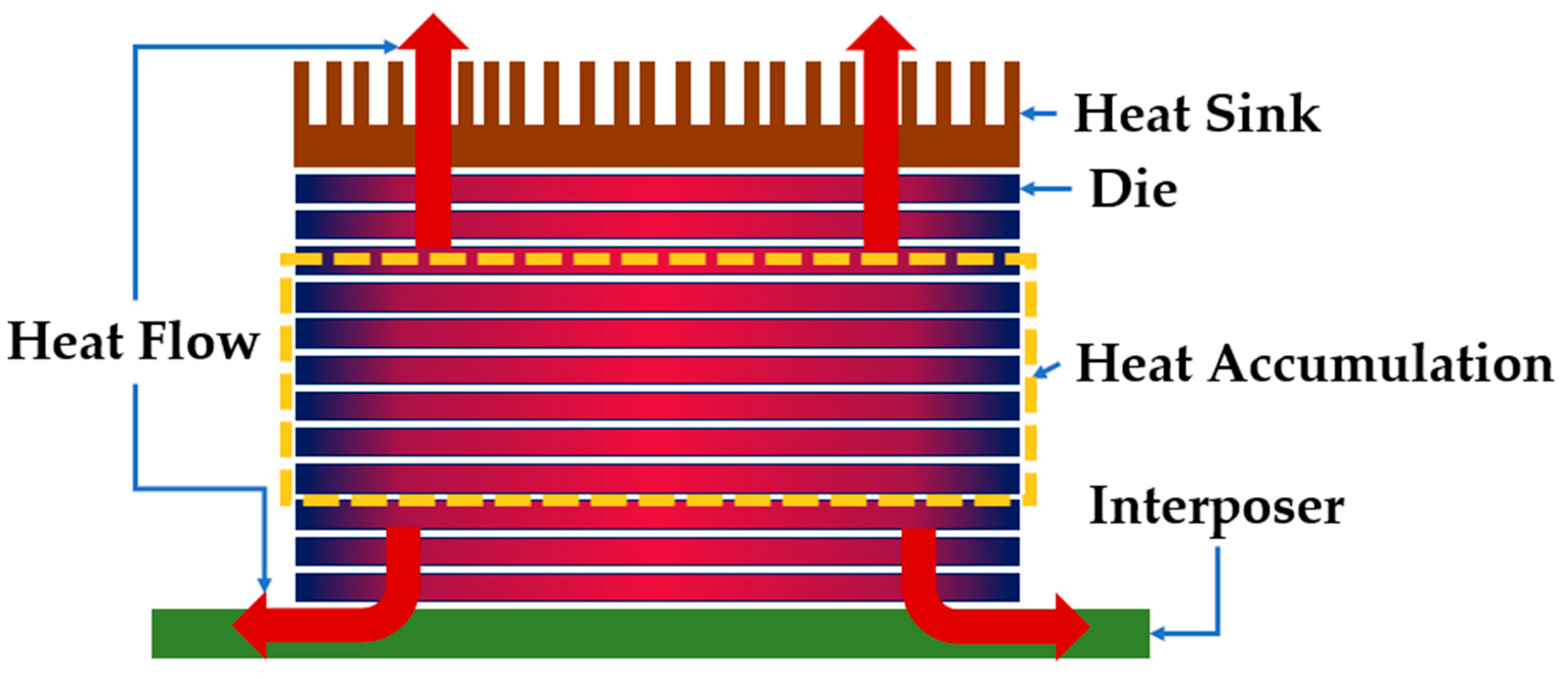
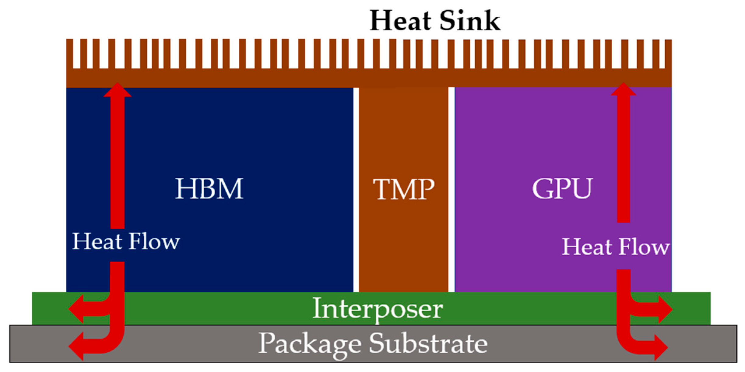
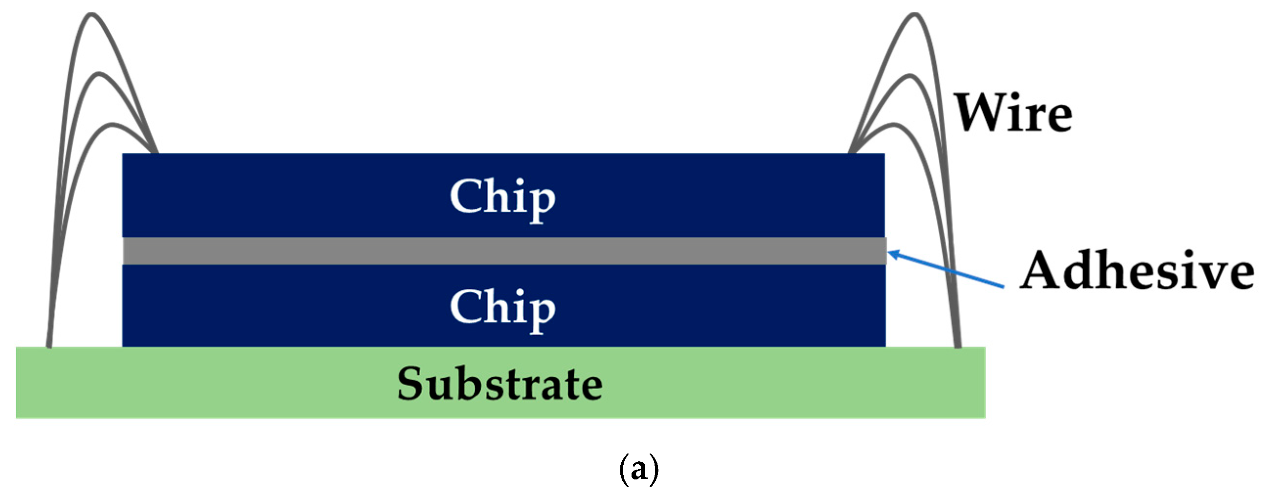

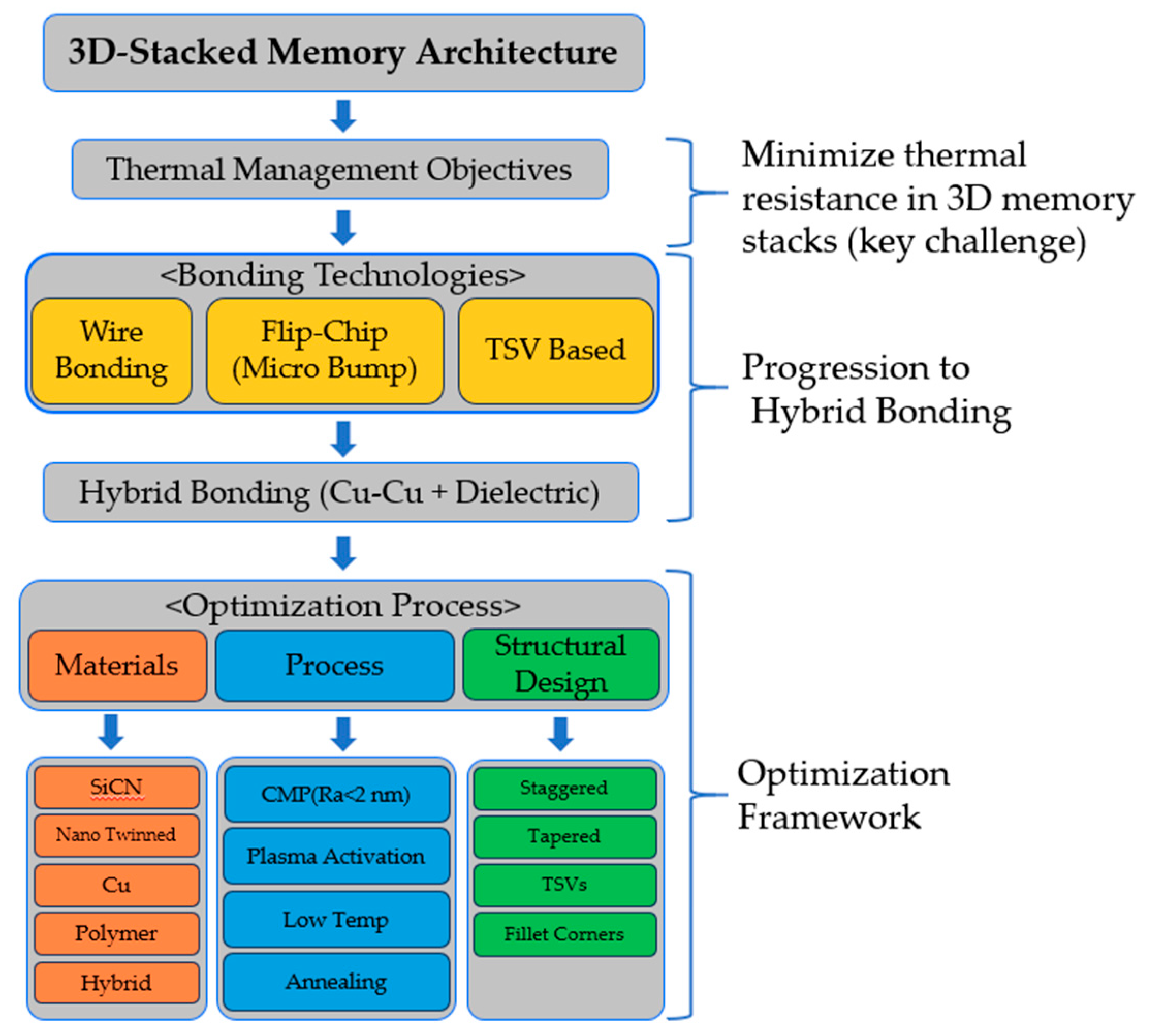

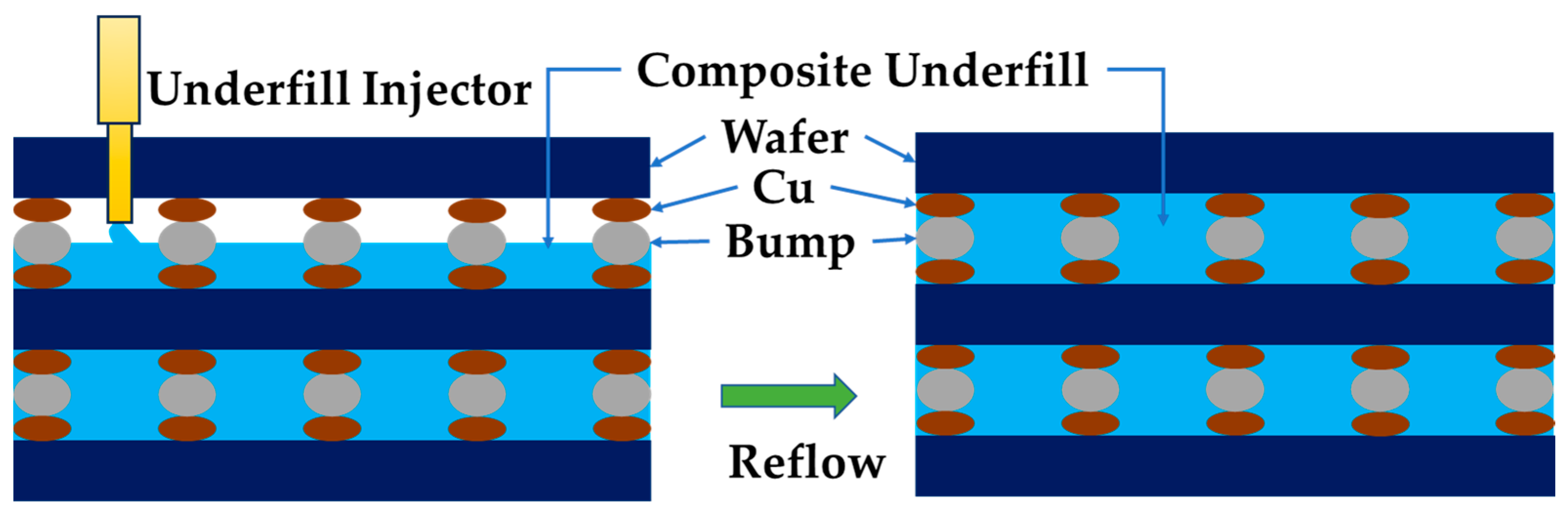
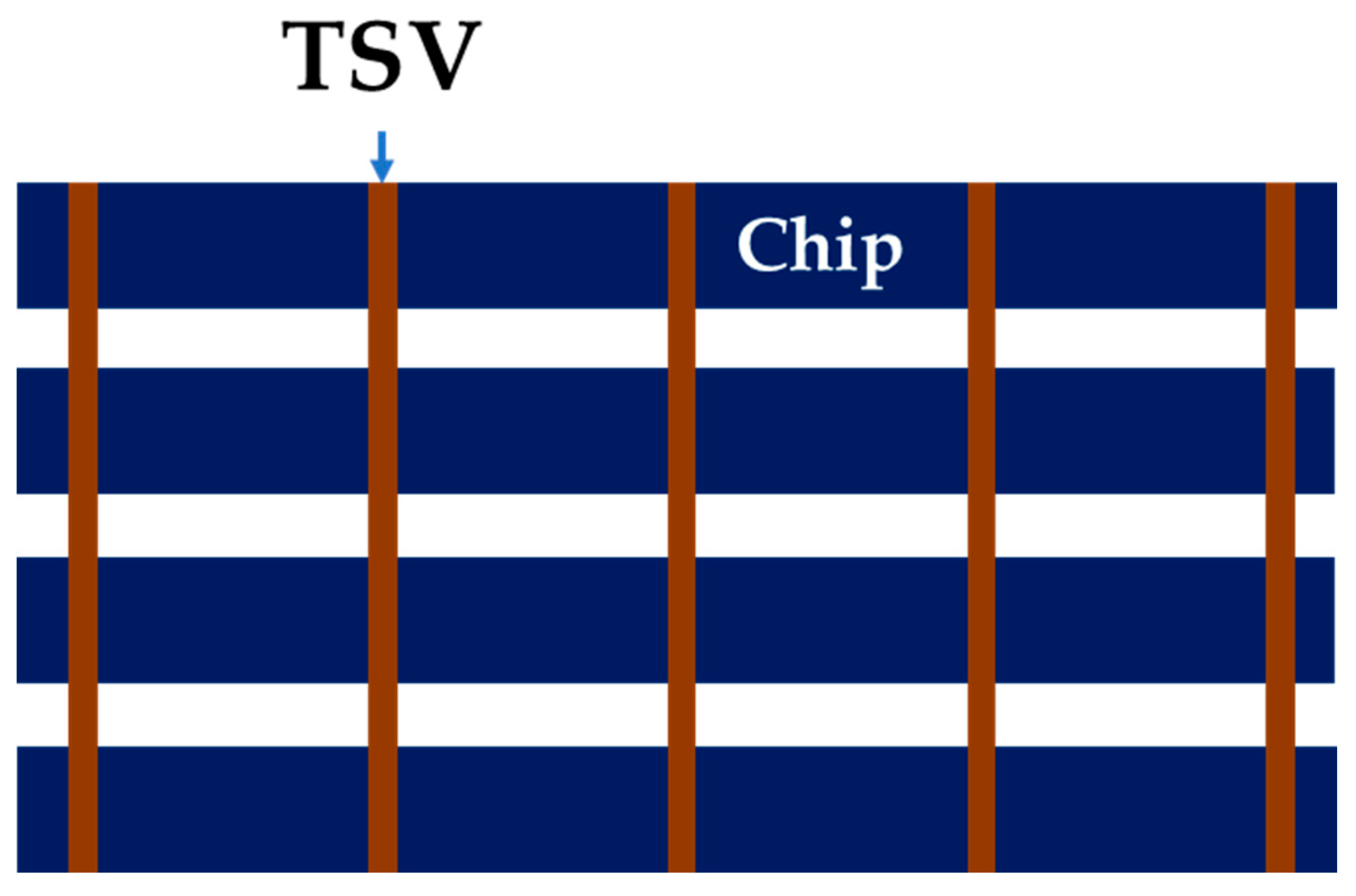
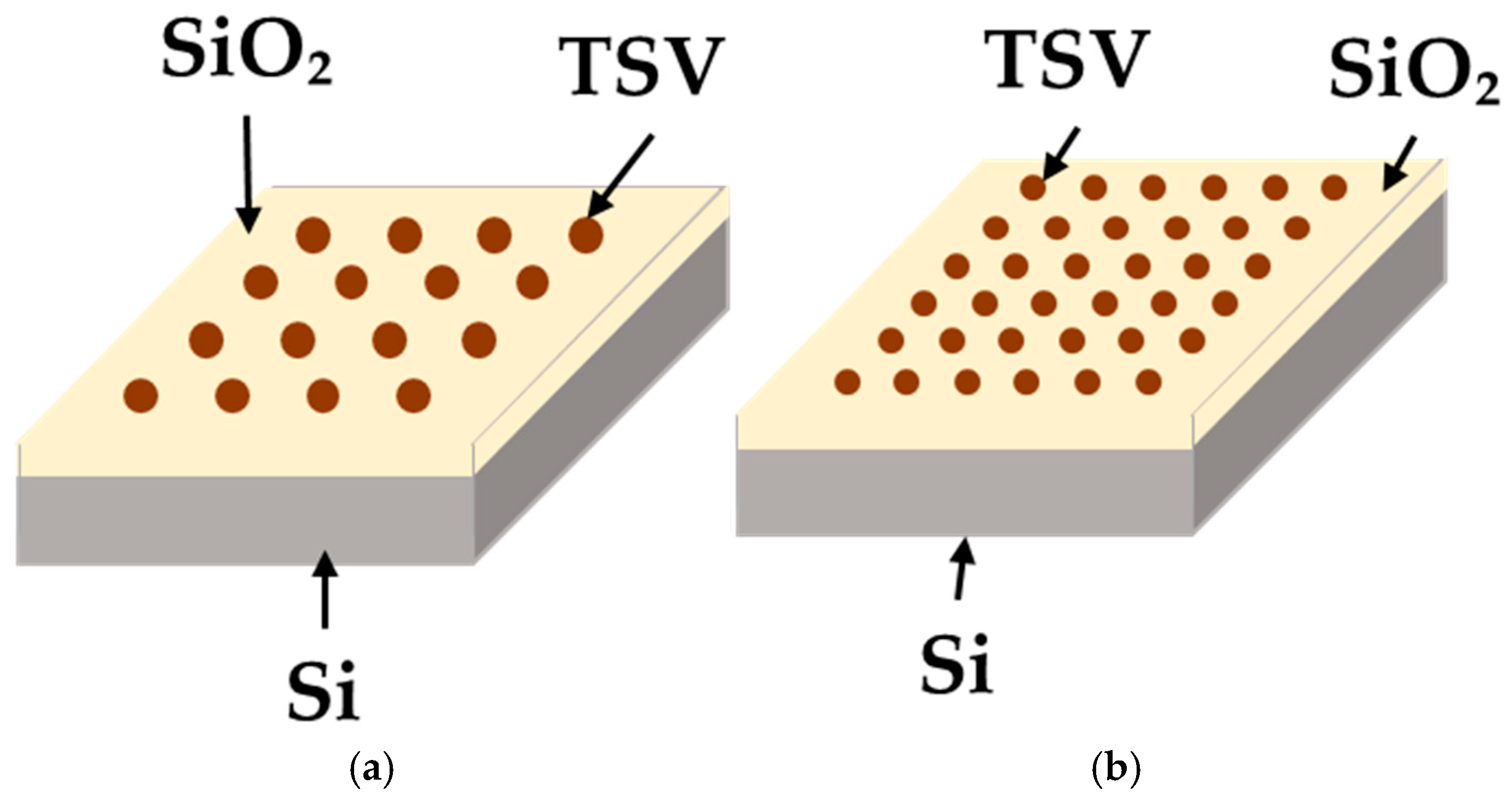
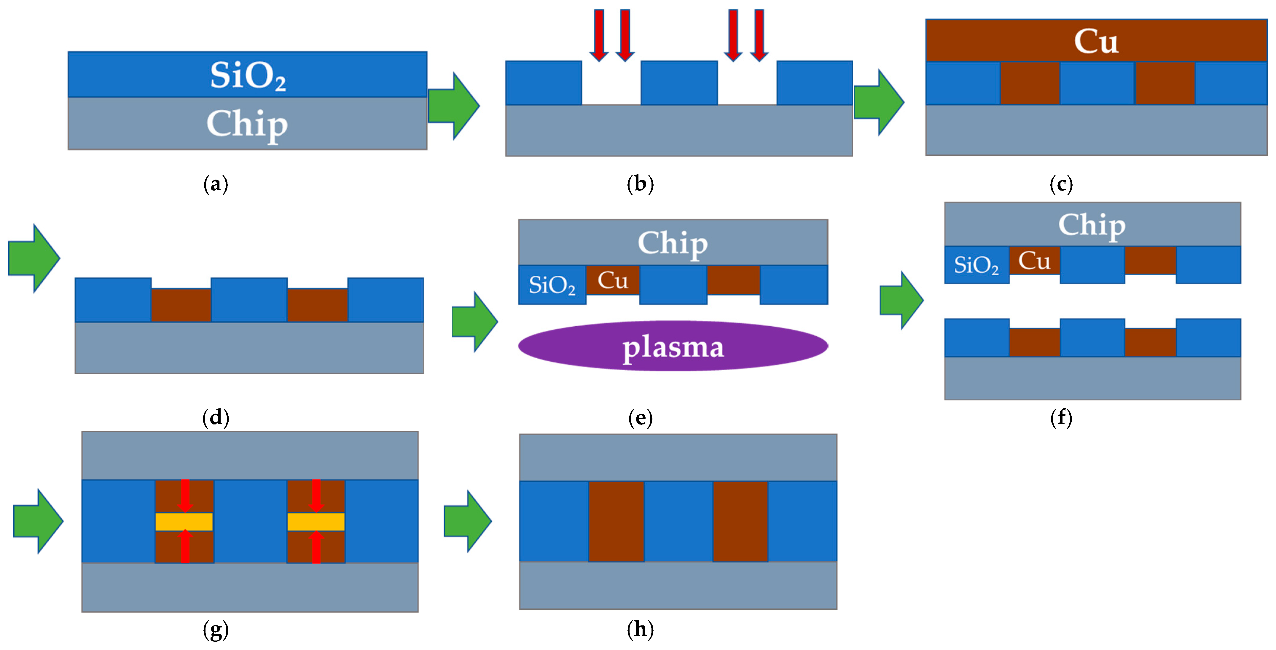
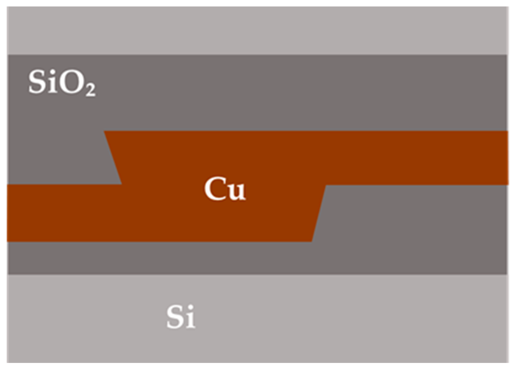
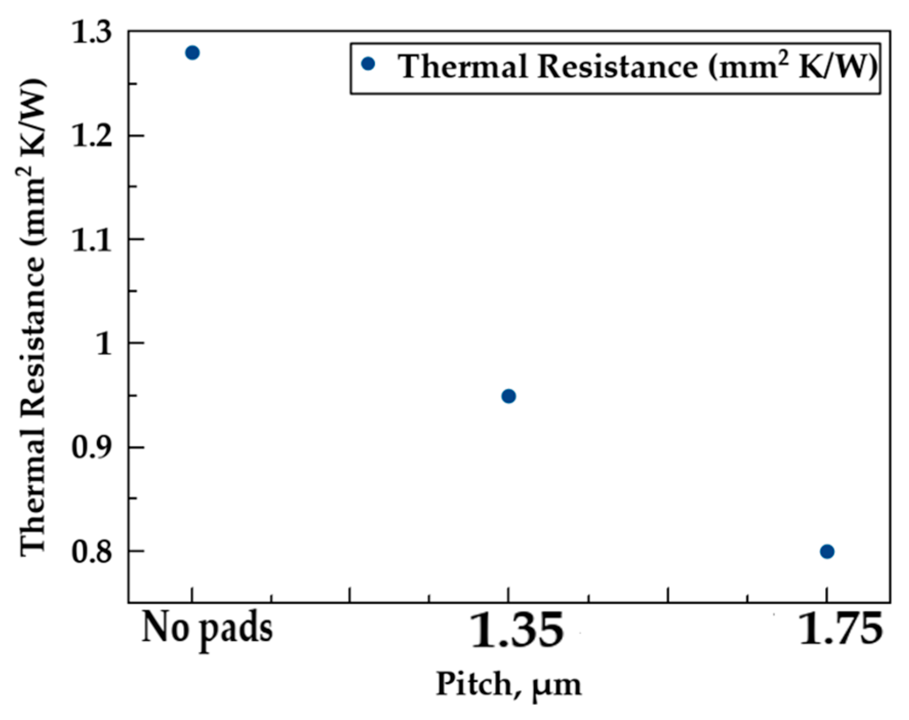
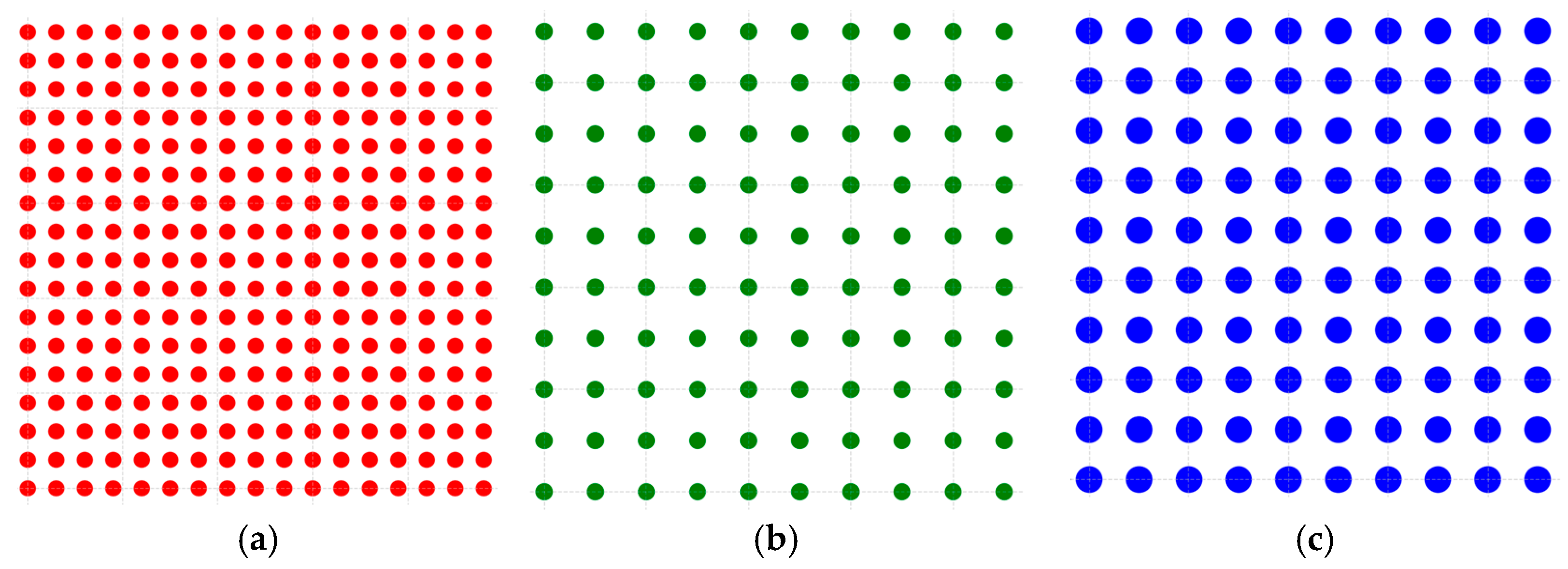

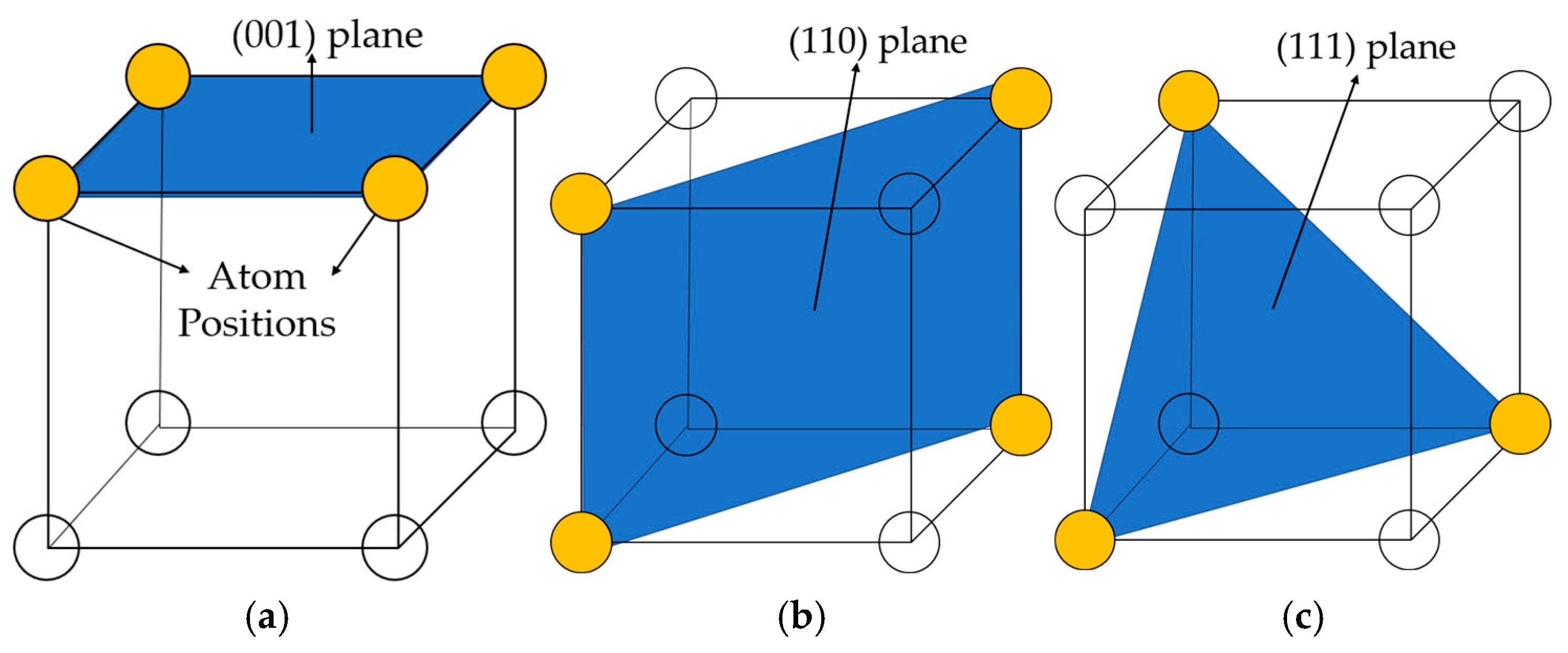
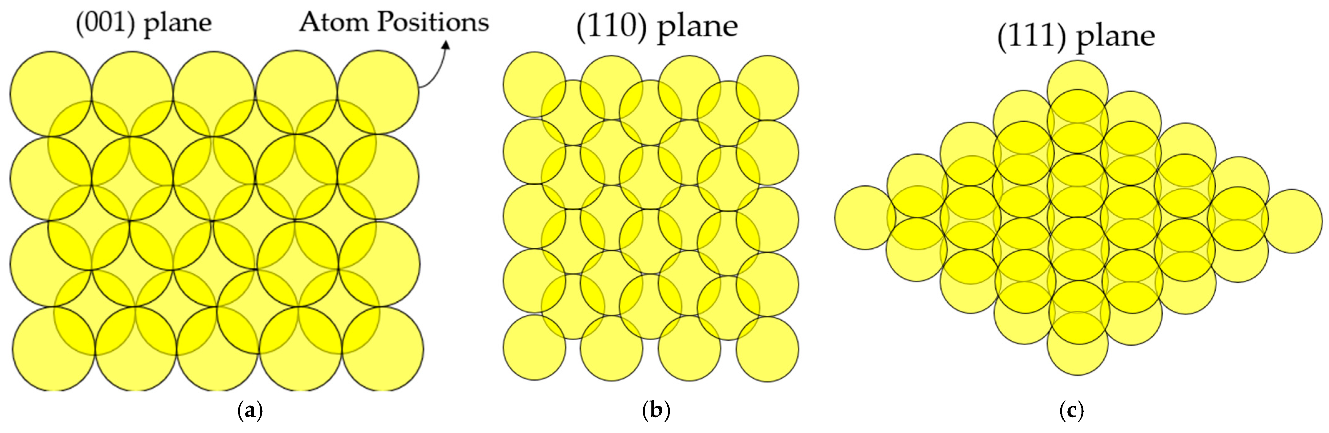

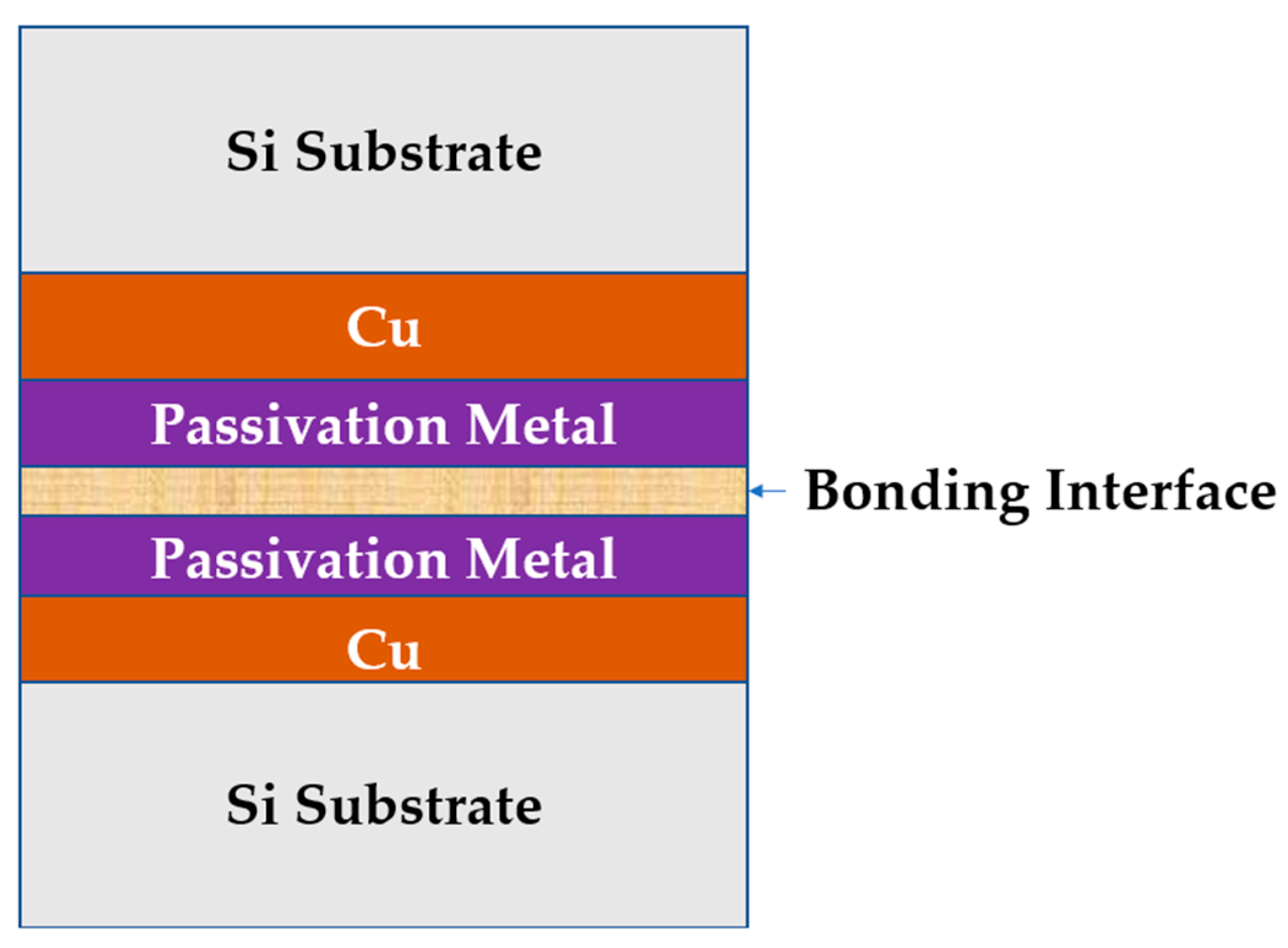
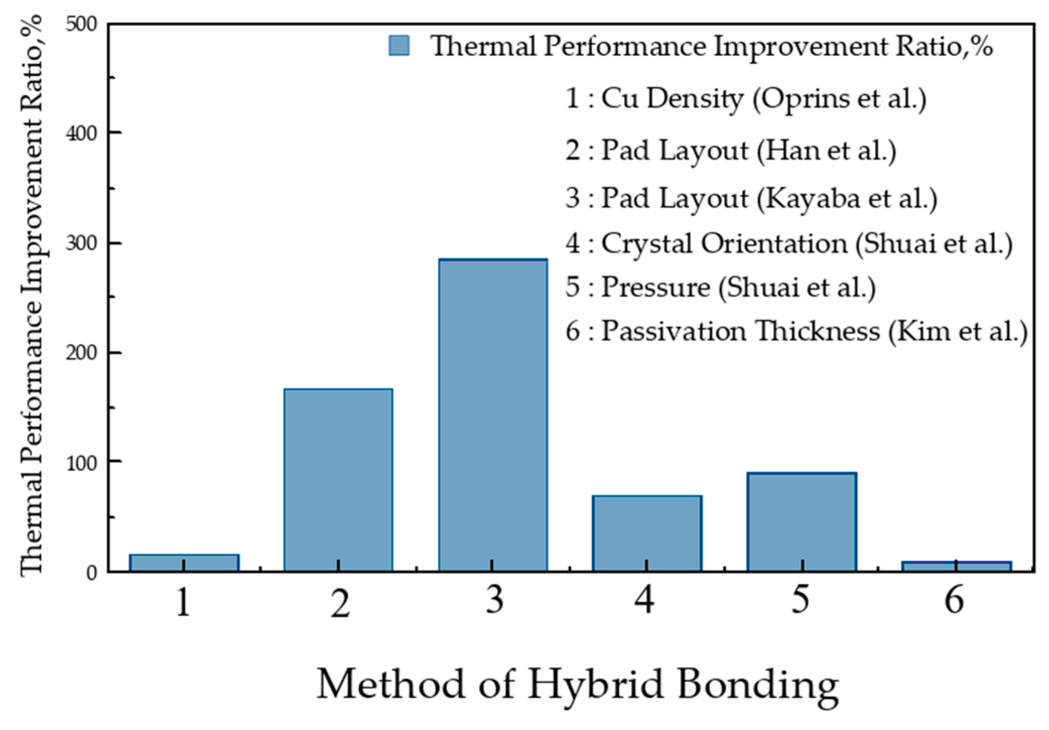


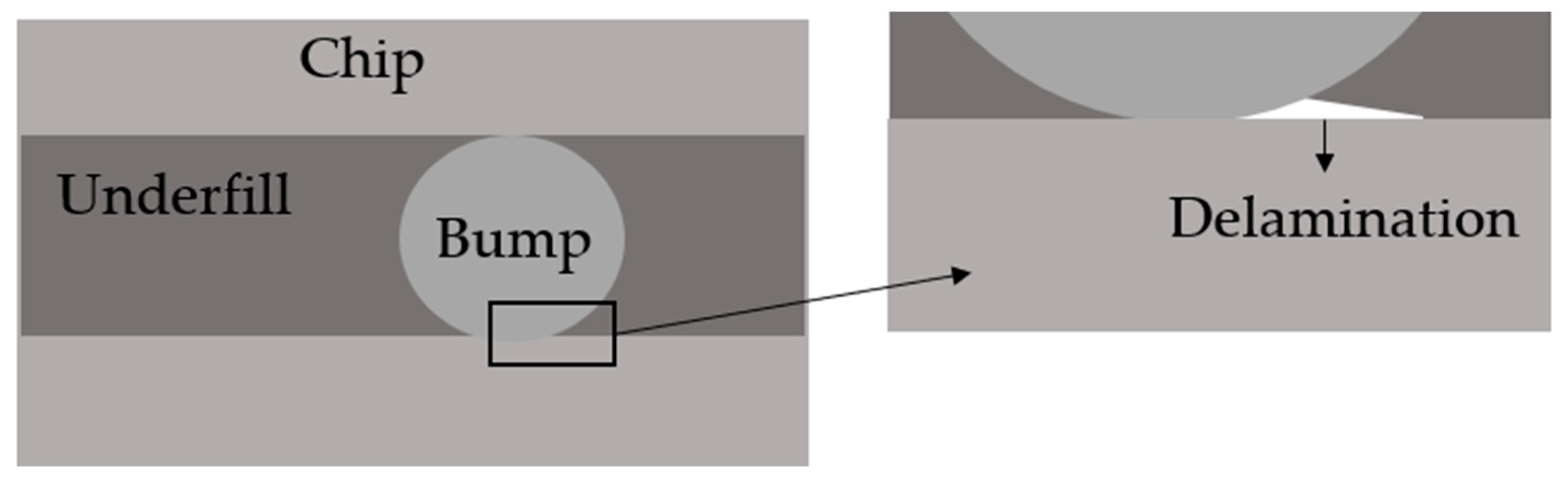


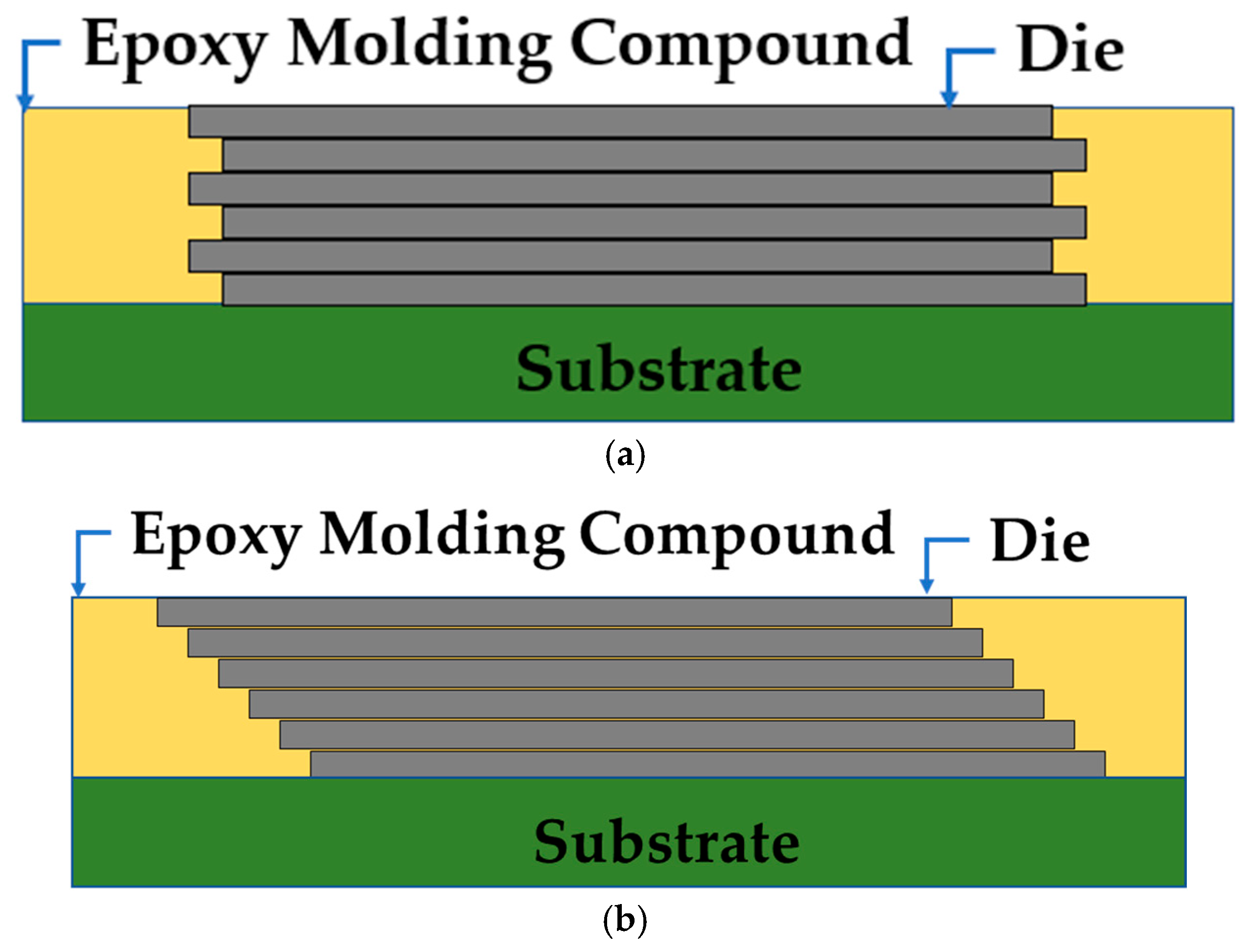
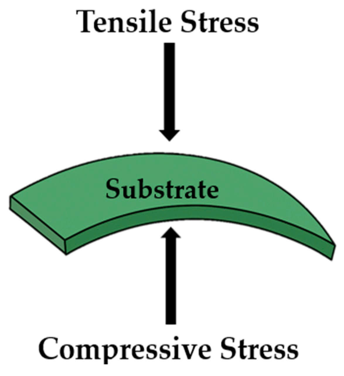
