Article

A Reflection-Based Ultra-Fast Measurement Method for the Continuous Characterization of Self-Heating for Advanced MOSFETs

1
College of Information Science and Electronic Engineering, Zhejiang University, Hangzhou 310027, China
2
School of Integrated Circuits, East China Normal University, Shanghai 200241, China
*
Author to whom correspondence should be addressed.
Electronics 2025, 14(13), 2634; https://doi.org/10.3390/electronics14132634
Submission received: 14 May 2025 / Revised: 13 June 2025 / Accepted: 16 June 2025 / Published: 30 June 2025
(This article belongs to the Section Semiconductor Devices)

Abstract

As semiconductor devices approach the sub-10 nm technology node, the self-heating effect (SHE) induced by confined geometries (e.g., FinFETs and nanosheet FETs) has emerged as a critical bottleneck affecting both performance and reliability. This challenge has prompted extensive research efforts to develop advanced characterization methodologies to investigate this effect and its corresponding influence on the device’s reliability issues. In this paper, we propose reflection-based ultra-fast measurement techniques for the continuous monitoring of the self-heating effect in advanced MOSFETs. With this approach, the self-heating effect-induced degradation of transistor drain current and the real-time temperature change can be continuously captured using a digital phosphor oscilloscope on a nanosecond scale. The thermal time constant of 17 ns and the thermal resistance of 34,000 K/W have been extracted for the short channel transistors used in this study with the help of this new characterization method. This reflection-based method is useful for the fast extraction of the thermal time constant and thermal resistance and for the continuous monitoring of current degradation as well as the real-time temperature. Therefore, this new characterization method is beneficial for the evaluation of the self-heating effect in advanced ultra-scaled MOSFETs.

1. Introduction

The self-heating effect (SHE) has been studied for more than 40 years [1,2,3]. At a macroscopic level, the drain current flow through a channel will generate heat and cause a local temperature rise. At the microscopic level, hot carriers undergo a scattering process in which they exchange energy with phonons, resulting in a local temperature rise [4]. Advanced CMOS technologies, such as Fully Depleted Silicon-On-Insulator (FDSOI), Fin Field-Effect Transistors (FinFETs), and Gate-All-Around Field-Effect Transistors (GAA-FETs), suffer from severe self-heating problems due to their ultra-scaled device dimensions, high power consumption, and poor heat dissipation [5,6,7,8,9]. The rise in device channel temperature is given by T r i s e = P D · R t h = I D · V D R t h , where R t h is the thermal resistance [10,11].
Hot Carrier Injection (HCI) and Bias Temperature Instability (BTI) are temperature-sensitive reliability issues in advanced nodes [12,13,14]. The SHE will degrade the saturation current and hence overestimate HCI degradation without temperature correction [15]. The SHE-induced high device temperature will exacerbate BTI’s contribution to the measured HCI degradation [6,16] and accelerate BTI recovery [17]. As the SHE is critical for the accurate characterization of transistor performance and reliability as well as circuit simulations [18], plenty of studies have been conducted to systematically study the SHE, including analytical and electrical methods. The thermal elements of analytical methods, such as Picosecond Imaging Circuit Analysis (PICA) [19], Scanning Thermal Microscopy [20], and Micro-Raman Spectroscopy [21], are associated with the luminescence or phonon process. In contrast, the thermal elements of electrical methods, such as the gate resistance method [22], pulsed I-V method [23], and AC conductance method [24,25], are associated with transistor basic electrical parameters. Each method has its own advantages and disadvantages depending on the characterization requirements and test setup.
Analytical methods have the characteristics of fast measurement speed and high time resolution in capturing self-heating phenomena. However, they usually require converting the change in optical signals to electrical parameters, which is challenging and non-straightforward, to realize accurate self-heating characterization. Electrical techniques have the advantage of directly characterizing the influence of the SHE on electrical parameters. However, the gate resistance method needs a good layout design. The conventional pulsed I-V method generally may not be sufficient to investigate the device with a thermal time constant τ t h < 100 ns. And the AC conductance method needs to convert the frequency domain result to the time domain.
In this paper, we propose a reflection-based ultra-fast characterization method for continuously monitoring the self-heating-induced degradation of transistor drain current. This method is compatible with basic transistor radio frequency (RF) measurements with the benefit of high temporal resolution. In this method, the high-frequency signal reflection is utilized instead of elimination, which is a common handling approach in RF tests.
Compared with traditional I-V measurement methods, the proposed reflection-based methodology enables dynamic real-time monitoring of the drain current degradation caused by the self-heating effect at the nanosecond scale. Additionally, accurate extraction of the thermal time constant can be efficiently performed. The overall measurement setup is structurally simple and seamlessly integrable with standard radio frequency (RF) test platforms, indicating strong potential for scalable and extended applications in advanced device characterization.

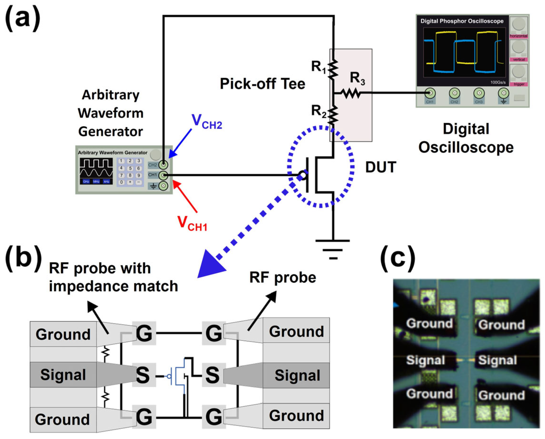
2. Experimental Setup

A reflection-based ultra-fast measurement methodology has been proposed for transistors’ I-V measurement on the nanosecond scale, which shows its significant potential in heat-free measurements. Note that in this study, heat-free means local self-heating has minimal impacts on the basic electric performance and reliability behavior since it takes several nanoseconds for local self-heating to increase the average channel temperature [5]. Figure 1a shows the adopted measurement setup. In order to achieve ultra-fast measurement, the generation of applied voltage pulses with a steep rise edge (small tr) and the instant capture of the corresponding output during the rise edge are essential. In this work, a small tr value of 200 ps is adopted. A high bandwidth arbitrary waveform generator (AWG) with multiple channels is used to supply voltage pulses to both gate and drain terminals through two separate channels, VCH1 and VCH2. The pick-off tee used here eliminates unnecessary reflection and acts as a power divider. A high bandwidth digital phosphor oscilloscope (DPO) is used to capture both incident and reflection signals. An RF probe with a 50 Ω impedance match is used in the gate pad, whereas a normal RF probe without an impedance match is used in the drain pad, as schematically shown in Figure 1b. To perform wafer-level RF measurements, short channel transistors used in this study are designed as a ground–signal–ground (GSG) layout, as shown in Figure 1c.
The pulse rise time is set to 200 ps to ensure that waveform acquisition occurs well within the initial nanoseconds of the device’s operation, before significant self-heating effects take place. The 1 m transmission line introduces a ~10 ns delay, enabling clear separation between incident and reflected waveforms. All components in the signal path are impedance-matched to 50 Ω to minimize undesired reflections and maintain signal integrity. These configurations support the underlying assumption that the Device Under Test (DUT) remains in a near-isothermal state during the early measurement window.

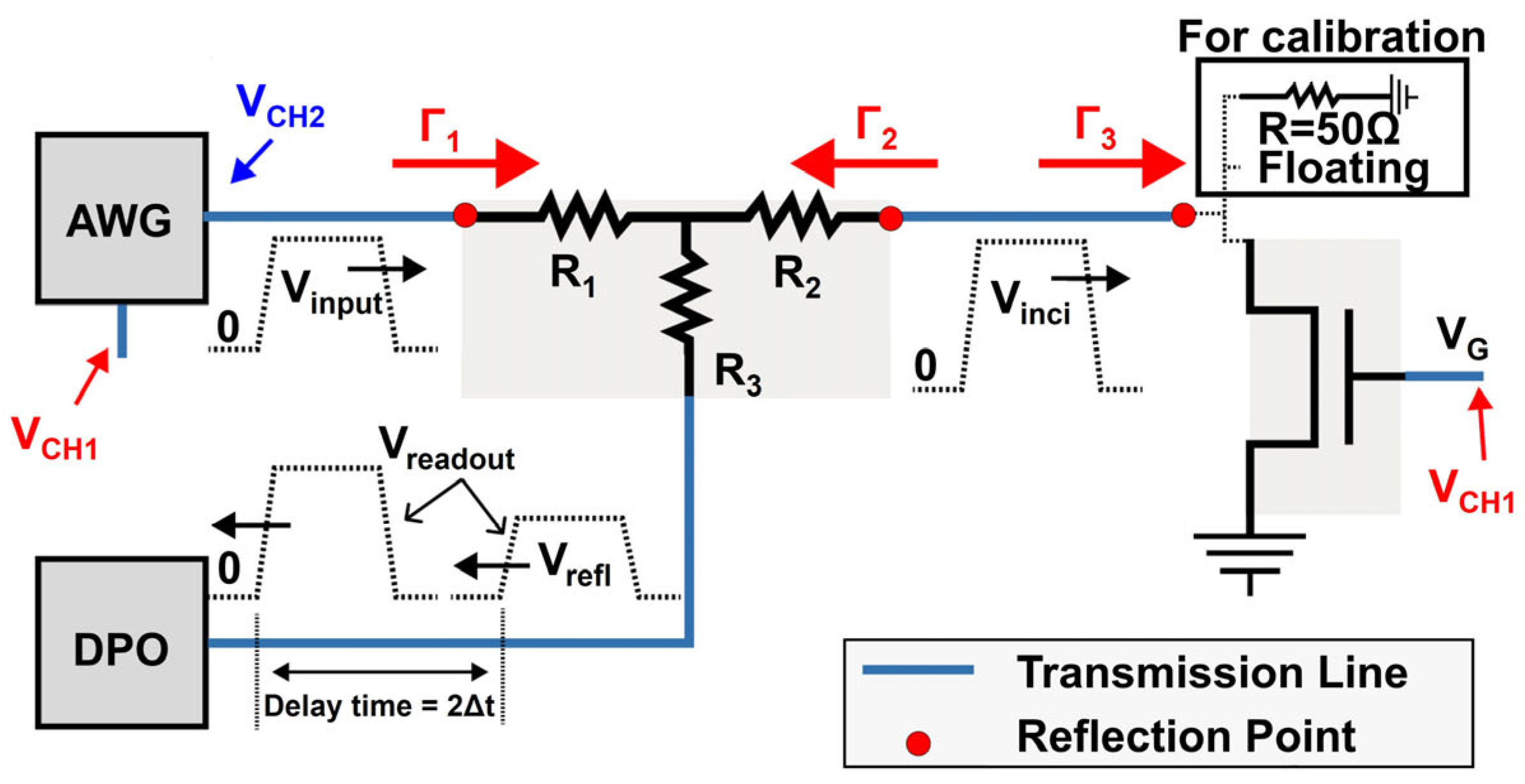
3. Reflection-Based Characterization Methodology

3.1. Reflection in the System

In this configuration, the signal of the gate side has no reflection from the AWG to the gate pad, ensuring its signal integrity. As for the drain side, there is a natural reflection due to the discontinuous resistance at the device drain terminal. This impedance mismatch inevitably leads to a signal reflection, which is mainly utilized to perform the measurements. All the three resistances, namely R1, R2, and R3, have a value of 16.7 Ω.
According to the transmission line theory, an electromagnetic wave will reflect at any point where the impedance is not matched. The reflection coefficient Γ is generally defined as Γ = ( Z o u t Z i n ) / Z o u t + Z i n = V r e f l e c t i o n / V i n c i d e n t . Figure 2 shows a waveform reflection sequence diagram. The input waveform named V i n p u t will first be reflected at the Γ 1 point and then go through the pick-off tee. It is divided into two identical parts called V i n c i . One of the incident waveforms arrives at the DPO through R 3 , and the other will be reflected at the device’s Γ 3 point. The reflected waveform called V r e f l will arrive at the DPO with a time delay of 2 Δ t , where Δ t is the time needed for the signal to pass through the one-meter-long transmission line once. In this configuration, Vinci represents the signal reaching the drain side of the DUT, while Vrefl is the waveform reflected due to the impedance mismatch at the device terminal, and both are measured at the DPO through the pick-off tee. The incident and reflection waveforms will be superimposed together, which obeys the principle of vector superposition. The superimposed incident and reflection waveforms were separated according to the calibration procedure described in the calibration section. These waveforms are then used to calculate the device-side reflection coefficient Γ 3 , which captures the impedance mismatch at the DUT terminal. According to the transmission line theory, the incident and reflected components satisfy V i n c i = V i n ( 1 + Γ ) and V r e f l = V i n · Γ . Based on this, the channel resistance R C , drain voltage V D , and drain current I D are computed using the expressions shown in Figure 3. Each equation in Figure 3 corresponds to a specific step in the drain current extraction process. Specifically, Equation (1) computes the incident voltage Vinci arriving at the drain terminal of the DUT based on the input waveform and the reflection coefficient Γ 1 at the first impedance discontinuity. Equation (2) calculates the reflected voltage Vrefl, which is influenced by multiple stages of impedance mismatch and contains information about the DUT’s internal channel resistance through the reflection coefficient Γ3. Equation (3) determines the drain voltage VD, derived from the superposition of the incident and reflected signals, expressed as V D = V i n c i   ·   ( 1 + Γ 3 ) . Equation (4) then applies Ohm’s law to obtain the drain current ID using the relationship I D = V D / R C , where RC is the extracted channel resistance. Finally, Equations (5)–(9) define the reflection coefficients Γ1, Γ2, and Γ3 and the equivalent parallel resistances RP1 and RP2, which are essential for modeling the signal path and enabling accurate computation. This complete formulation provides a transparent and physically grounded approach for extracting real-time current characteristics from high-speed waveform measurements.
The formulas used to compute the drain current ID are as follows:
V inci =   V input ( 1 + Γ 1 ) R P 1 R 1 + R P 1 Z 0 Z 0 + R 3
V refl =   V input ( 1 + Γ 1 ) R P 1 R 1 + R P 1 Z 0 Z 0 + R 2 Γ 3 ( 1 + Γ 2 ) R P 2 R 2 + R P 2 Z 0 Z 0 + R 3
V D =   V input 1 + Γ 1 R P 1 R 1 + R P 1 Z 0 Z 0 + R 2 ( 1 + Γ 3 )
I D = V D R C
Γ 1   = R 1 + R P 1 Z 0 R 1 + R P 1 + Z 0
Γ 2   = R 2 + R P 2 Z 0 R 2 + R P 2 + Z 0
Γ 3 = R C Z 0 R C + Z 0
R P 1 = 1 / ( 1 R 3 + Z 0 + 1 R 2 + Z 0 )
R P 2 = 1 / ( 1 R 1 + Z 0 + 1 R 2 + Z 0 )
Parameter Definitions:
In Equations (1)–(9), the following symbols are used:
  • Vinci: The incident voltage reaching the drain side of the DUT (unit: V).
  • Vrefl: The reflected voltage due to impedance mismatch at the DUT (unit: V).
  • Γ1, Γ2, Γ3: The reflection coefficients at different impedance discontinuities, with dimensionless ratios defined as Γ = ( Z Z 0 ) / Z + Z 0 , where Z is the local impedance and Z0 = 50 Ω is the characteristic impedance.
  • RC: The channel resistance of the DUT, extracted from the waveform superposition (unit: Ω).
  • VD: The instantaneous drain voltage at the device terminal (unit: V).
  • ID: The drain current calculated using Ohm’s law (unit: A).
  • R1, R2, R3: The resistors in the pick-off tee, each 16.7 Ω.
  • RP1, RP2: Parallel equivalent resistances of the resistive divider branches (unit: Ω).
  • Z0: The characteristic impedance of the transmission line, fixed to 50 Ω.

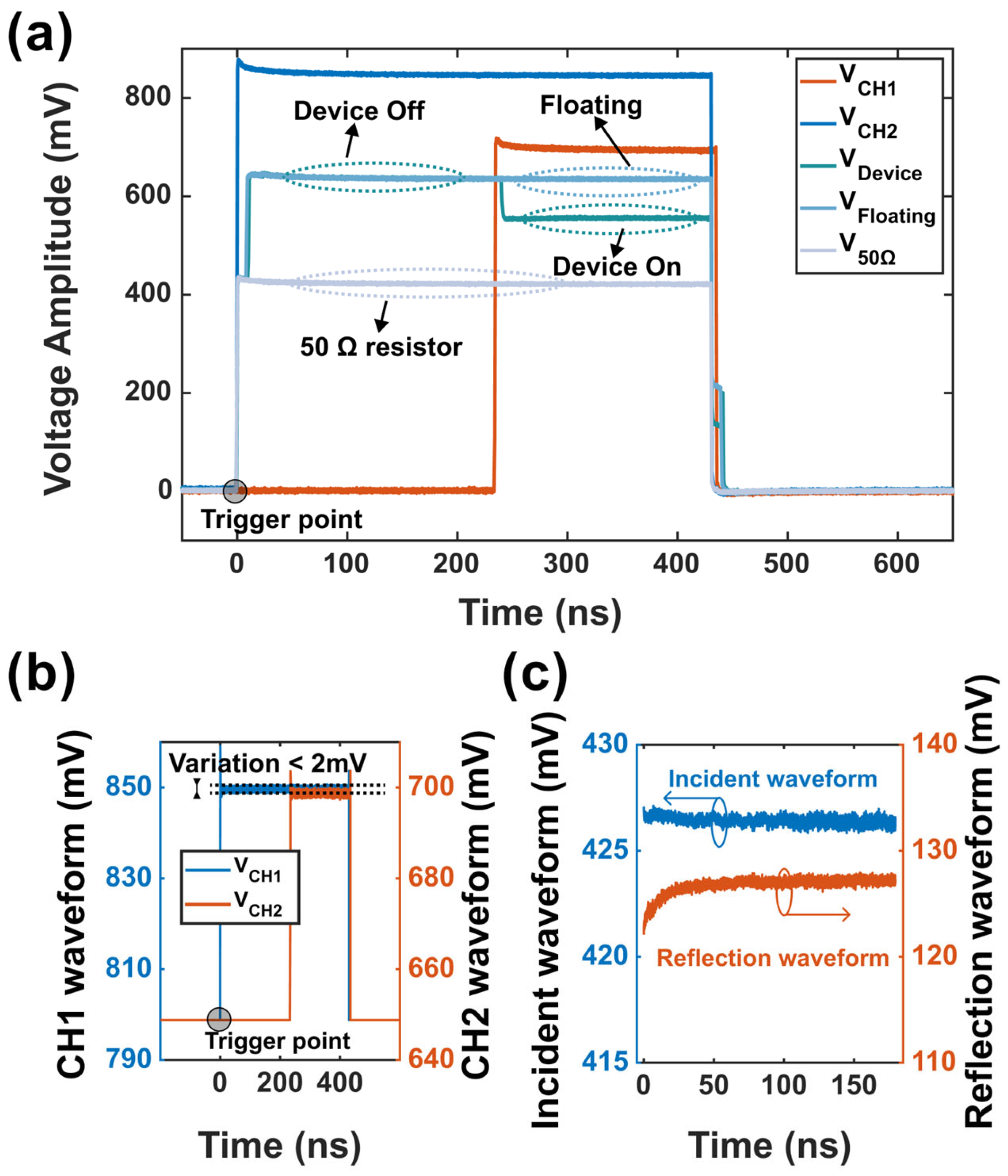
3.2. The Calibration of the Measurement System

The waveforms generated by the AWG are shown in Figure 3a, labeled as VCH1 and VCH2, respectively. VCH2 is generated by the AWG CH1 channel and applied to the device gate terminal directly, whereas VCH2 is generated by the AWG CH2 channel and applied to the device drain terminal through a pick-off tee, as shown in Figure 2. Figure 3b shows the real waveform used in our test. The waveform was carefully tuned to ensure the voltage variation remained within 2 mV across a total swing of 850 mV (less than 0.24%), ensuring sufficient stability for reflection-based measurement.
A standard 50 Ω resistor and floating transmission line replace the device under test to calibrate the divider losses and cable losses, as shown in the upper right in Figure 2. The superimposed incident and reflection waveforms were extracted from the DPO readout data based on the reference waveforms. V50Ω data is used as the incident waveform, and ( V device o n V 50 ) data is used as the reflection waveform. The separated incident and reflection waveforms are shown in Figure 3c.

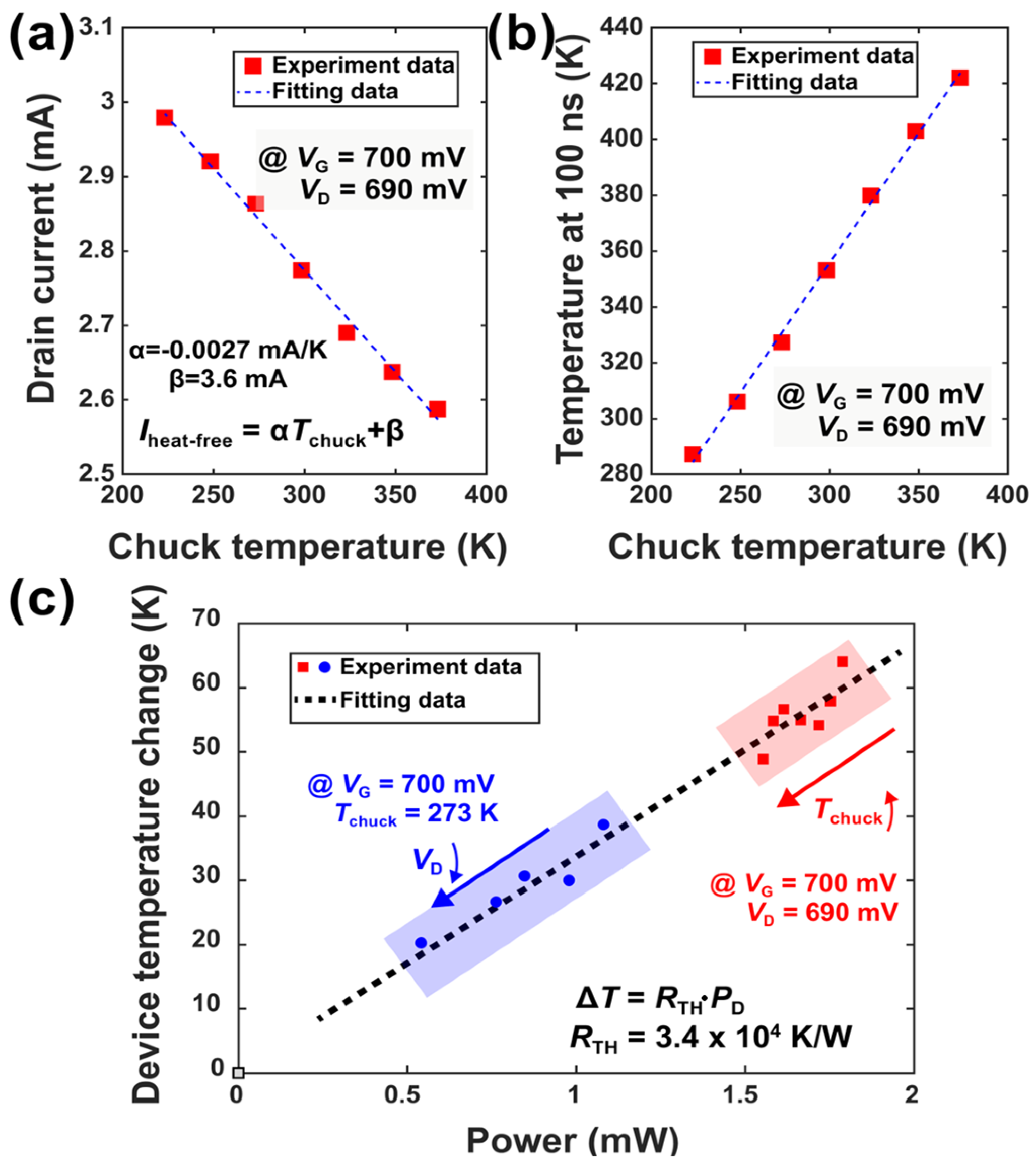
4. Results and Discussion

The proposed methodology is demonstrated to characterize the self-heating effect of commercial-ready scaled transistors. Figure 4 shows the drain current degradation versus the time at different chuck temperatures, ranging from 223 K to 373 K. The drain current ID decreases rapidly at the first 50 ns once the device is on, which can be mainly attributed to the local self-heating and elevated device temperature. The 63.2% current degradation is used as a criterion to extract the thermal time constant τ t h , corresponding to the classic solution of a first-order thermal RC network under a step power input, where the thermal time constant τth is defined as the time required for the temperature to rise to 63.2% of its final steady-state value. And the τ t h value of the devices in Figure 4 is about 17 ns.
The drain current at time zero, shown as circles in Figure 4, was used as the heat-free current at different chuck temperatures. By changing the chuck temperature, a cluster of ID traces was obtained. And the heat-free current can be extracted for different chuck temperatures. Therefore, the heat-free current versus the chuck temperature can be derived, as shown in Figure 5a. This relationship can be modeled as a linear relationship of the heat-free drain current to chuck temperature as I h e a t - f r e e = α T c h u c k + β mathematically. And the real-time temperature of the device is evaluated by T d e v i c e ( t ) = I r e a l t i m e ( t ) β / α with the fitting parameters α = 0.0027 mA/K and β = 3.6 mA. Specifically, α and β are obtained by performing linear regression between the heat-free drain current (extracted at t = 0 ) and the chuck temperature, as shown in Figure 5a. The linear fitting yields α =   0.0027 mA/K and β = 3.6 mA, with a high R 2 value indicating good agreement. These parameters are treated as constants over the tested temperature range (223 K to 373 K) due to the strong linearity observed.
The steady temperature versus chuck temperature is shown in Figure 5b. Here, the steady temperatures are extracted from the temperature at 100 ns, where thermal generation and dissipation come to an equilibrium state. The device channel temperature change at different levels of device power dissipation is shown in Figure 5c. Red dots were acquired by changing the chuck temperature at constant VG and VD values. Blue squares were acquired at the same 273 k value but with different VD values for various powers.
To characterize the thermal resistance R t h , we first calculated the real-time temperature using the extracted α and β values and then fit the temperature rise ( Δ T = T d e v i c e T c h u c k [K]) against power dissipation ( P D W = I D [ A ] · V D [ V ] ) based on the relation Δ T [ K ] = R t h [ K / W ] · P D [ W ] , where ΔT is the increasing temperature and P D is power dissipation. The thermal resistance extracted from the experiment data is about 3.4 × 10 4 K/W, which is reliable compared with previous results of ultra-scaled MOSFETs [9,15]. The steady-state current degradation in this study is primarily ascribed to self-heating, while other slow degradation mechanisms are considered negligible due to the short test duration and fixed bias conditions. To improve measurement reliability, the setup was optimized based on a previously validated reflection-based nanosecond-scale method, with key error sources being systematically addressed. All signal paths were impedance-matched to 50 Ω, except for the drain side, where intentional mismatch enabled the extraction of reflection signals. Calibration using two terminations (50 Ω load and floating) confirmed the accuracy of the reflection coefficient model. The architecture further distinguishes the primary reflection point ( Γ 3 ) from parasitic ones ( Γ 1 ,     Γ 2 ), which are effectively suppressed via the pick-off tee.
Previous comparative studies [26] showed that this method yields a slightly higher drain current (~14%) than commercial systems such as the B1500 due to reduced thermal stress under nanosecond pulses. With impedance control, timing synchronization, and waveform averaging, measurement uncertainty is minimized, ensuring accurate thermal parameter extraction.
Compared with the conventional SHE characterization method, the proposed reflection-based ultra-fast technique exhibits notable advantages in both temporal resolution and experimental simplicity. Analytical techniques such as Micro-Raman Spectroscopy and PICA offer high spatial and temporal resolution but rely on indirect optical-to-electrical conversions, which often require complex calibration and are difficult to integrate into standard test platforms. Moreover, as device dimensions continue to be scaled into the deep sub-10 nm regime, optical-based methods such as Micro-Raman and PICA face intrinsic limitations due to the laser spot size and heat diffusion effects, which constrain their spatial resolution and localization accuracy. Under such extreme nanoscale conditions, the reflection-based electrical method proposed in this study operates independently of optical alignment and the laser spot size, offering strong dimensional scalability. As a result, it is particularly well-suited for dynamic thermal characterization in ultra-scaled transistor structures. Electrical techniques, including the gate resistance method, pulsed I-V measurements, and AC conductance methods, are more directly tied to transistor electrical behavior but suffer from critical limitations. For instance, conventional pulsed I-V methods typically lack the time resolution necessary to resolve sub-100 ns thermal transients, and AC conductance measurements require complex post-processing to convert frequency-domain data into time-domain thermal responses [27]. In contrast, our method enables the direct, real-time monitoring of drain current degradation due to self-heating by utilizing high-frequency signal reflections—a phenomenon usually suppressed in RF measurements. This not only circumvents the complexity of optical calibration and frequency-domain transformations but also allows for seamless integration with existing RF measurement setups. The demonstrated ability to extract thermal time constants as short as 17 ns highlights the method’s suitability for emerging nanoscale transistor technologies, making it a promising tool for fast, accurate, and scalable self-heating characterization.
The measurement setup is structurally simple and compatible with standard RF test platforms, making it highly integrable and scalable. These features highlight the method’s potential as a reliable and efficient tool for next-generation transistor thermal reliability assessment and circuit-level modeling.
Benefiting from its nanosecond-scale temporal resolution and sensitivity to transient signal behavior, the method demonstrates strong potential in both RF and High-Performance Computing (HPC) domains. In RF systems, it can be used for a rapid analysis of signal reflections and impedance discontinuities. In HPC platforms, it may assist in evaluating signal integrity issues in high-speed interconnects and memory interfaces, thereby contributing to improved system stability and reliability.
This work provides not only a novel perspective for self-heating evaluation but also a practical foundation for future research and industrial implementation in nanoscale device diagnostics [28].

5. Conclusions

This paper presents a reflection-based, ultra-fast method for the non-intrusive characterization of self-heating effects (SHEs) in advanced FinFET devices. By analyzing waveform reflections within a standard RF-accessible structure, the method enables the real-time monitoring of drain current degradation with nanosecond-scale temporal resolution. The extracted thermal time constant of approximately 17 ns underscores the need for high-speed measurements for heat-free characterization. Compared to conventional approaches, the proposed technique eliminates the need for optical setups or frequency-domain modeling, offering enhanced simplicity, accuracy, and compatibility with future nanoscale CMOS technologies.

Author Contributions

Conceptualization, W.L., G.H., Y.D., and C.Y.; methodology, W.L.; formal analysis, W.L., G.H., and Y.Z.; data curation, W.L. and G.H.; writing—original draft preparation, W.L.; writing—review and editing—Y.Z., G.H., X.Y., L.Z., Y.D. and W.L. All authors have read and agreed to the published version of the manuscript.

Funding

This work was supported by the National Key Research and Development Program of China under Grant 2020AAA0109001 and in supported part by the “Pioneer” and “Leading Goose” R&D Program of Zhejiang Province under Grant 2023C01018.

Data Availability Statement

The original contributions presented in this study are included in the article. Further inquiries can be directed to the corresponding author.

Conflicts of Interest

The authors declare no conflicts of interest.

References

  1. Negro, V.; Pannone, L. Self-Heating and Gate Leakage Current in a Guarded MOSFET. Proc. IEEE 1972, 60, 342–343. [Google Scholar] [CrossRef]
  2. Lidback, C.A.C. Scanning infrared microscopy techniques for semiconductor thermal analysis. In Proceedings of the 17th International Reliability Physics Symposium (IRPS), San Diego, CA, USA, 24–26 April 1979; pp. 183–189. [Google Scholar] [CrossRef]
  3. Mautry, P.; Trager, J. Self-heating and temperature measurement in sub-mm-MOSFETs. In Proceedings of the 19th European Solid State Device Research Conference (ESSDERC ’89), Berlin, Germany, 11–14 September 1989; pp. 675–678. [Google Scholar] [CrossRef]
  4. Prasad, C. A review of self-heating effects in advanced CMOS technologies. IEEE Trans. Electron Devices 2019, 66, 4546–4555. [Google Scholar] [CrossRef]
  5. Qu, Y.; Lin, X.; Li, J.; Cheng, R.; Yu, X.; Zheng, Z.; Lu, J.; Chen, B.; Zhao, Y. Ultra-fast (<1 ns) electrical characterization of self-heating effect and its impact on hot carrier injection in 14 nm FinFETs. In Proceedings of the 2017 IEEE International Electron Devices Meeting (IEDM), San Francisco, CA, USA, 2–6 December 2017; pp. 39.2.1–39.2.4. [Google Scholar] [CrossRef]
  6. Choudhury, N.; Sharma, U.; Zhou, H.; Southwick, R.G.; Wang, M.; Mahapatra, S. Analysis of BTI, SHE induced BTI and HCD under full VG/VD space in GAA nano-sheet N and P FETs. In Proceedings of the 2020 IEEE International Reliability Physics Symposium (IRPS), Dallas, TX, USA, 28 April 2020–30 May 2020; pp. 1–6. [Google Scholar] [CrossRef]
  7. Federspiel, X.; Torrente, G.; Arfaoui, W.; Cacho, F.; Huard, V. Temperature sense effect in HCI self-heating deconvolution: Application to 28 nm FDSOI. In Proceedings of the 2016 IEEE International Reliability Physics Symposium (IRPS), Pasadena, CA, USA, 17–21 April 2016; p. XT–09-1–XT-09-4. [Google Scholar] [CrossRef]
  8. Arfaoui, W.; Bossu, G.; Muhlhoff, A.; Lipp, D.; Manuwald, R.; Chen, T.; Nigam, T.; Siddabathula, M. A novel HCI reliability model for RF/mmWave applications in FDSOI technology. In Proceedings of the 2020 IEEE International Reliability Physics Symposium (IRPS), Dallas, TX, USA, 28 April 2020–30 May 2020. [Google Scholar] [CrossRef]
  9. Zhao, Y.; Qu, Y. Impact of self-heating effect on transistor characterization and reliability issues in sub-10 nm technology nodes. IEEE J. Electron Devices Soc. 2019, 7, 829–836. [Google Scholar] [CrossRef]
  10. Jin, W.; Fung, S.; Liu, W.; Chan, P.; Hu, C. Self-heating characterization for SOI MOSFET based on AC output conductance. In Proceedings of the International Electron Devices Meeting (IEDM), Washington, DC, USA, 5–8 December 1999; pp. 175–178. [Google Scholar] [CrossRef]
  11. Baylis, C.; Dunleavy, L.; Daniel, J. Direct measurement of thermal circuit parameters using pulsed IV and the normalized difference unit. In Proceedings of the 2004 IEEE MTT-S International Microwave Symposium Digest, Fort Worth, TX, USA, 6–11 June 2004; Volume 2, pp. 1233–1236. [Google Scholar] [CrossRef]
  12. Tyaginov, S.; Jech, M.; Franco, J.; Sharma, P.; Kaczer, B.; Grasser, T. Understanding and modeling the temperature behavior of hot-carrier degradation in SiON nMOSFETs. IEEE Electron Device Lett. 2016, 37, 84–87. [Google Scholar] [CrossRef]
  13. Alam, M.A.; Mahapatra, S. A comprehensive model of PMOS NBTI degradation. Microelectron. Reliab. 2005, 45, 71–81. [Google Scholar] [CrossRef]
  14. Wang, D.; Zhou, L.; Xue, Y.; Ren, P.; Sun, Z.; Wang, Z.; Wang, J.; Wu, B.; Ji, Z.; Wang, R.; et al. On the understanding of defects in short-term negative bias temperature instability (NBTI) for sub-20-nm DRAM technology. IEEE Electron Device Lett. 2023, 44, 1. [Google Scholar] [CrossRef]
  15. Jiang, H.; Liu, X.; Xu, N.; He, Y.; Du, G.; Zhang, X. Investigation of Self-Heating Effect on Hot Carrier Degradation in Multiple-Fin SOI FinFETs. IEEE Electron Device Lett. 2015, 36, 1258–1260. [Google Scholar] [CrossRef]
  16. Son, D.; Hong, K.; Shim, H.; Pae, S.; Shin, H. New insight into negative bias temperature instability degradation during self-heating in nanoscale bulk FinFETs. IEEE Electron Device Lett. 2019, 40, 1354–1357. [Google Scholar] [CrossRef]
  17. Liu, S.E.; Wang, J.S.; Lu, Y.R.; Huang, D.S.; Huang, C.F.; Hsieh, W.H.; Lee, J.H.; Tsai, Y.S.; Shih, J.R.; Lee, Y.H.; et al. Self-heating effect in FinFETs and its impact on devices reliability characterization. In Proceedings of the 2014 IEEE International Reliability Physics Symposium (IRPS), Waikoloa, HI, USA, 1–5 June 2014; pp. 4A.4.1–4A.4.4. [Google Scholar] [CrossRef]
  18. Prakash, O.; Dabhi, C.K.; Chauhan, Y.S.; Amrouch, H. Transistor self-heating: The rising challenge for semiconductor testing. In Proceedings of the 2021 IEEE 39th VLSI Test Symposium (VTS), San Diego, CA, USA, 25–28 April 2021; pp. 1–7. [Google Scholar] [CrossRef]
  19. Polonsky, S.; Jenkins, K. Time-resolved measurements of self-heating in SOI and strained-silicon MOSFETs using photon emission microscopy. IEEE Electron Device Lett. 2004, 25, 208–210. [Google Scholar] [CrossRef]
  20. Gotsmann, B.; Menges, F.; Karg, S.; Troncale, V.; Lantz, M.; Mensch, P.; Schmid, H.; Das Kanungo, P.; Drechsler, U.; Schmidt, V.; et al. Heat dissipation and thermometry in nanosystems: When interfaces dominate. In Proceedings of the 71st Device Research Conference (DRC), Notre Dame, IN, USA, 23–26 June 2013; pp. 231–232. [Google Scholar] [CrossRef]
  21. Sarua, A.; Ji, H.; Kuball, M.; Uren, M.; Martin, T.; Hilton, K.; Balmer, R. Integrated micro-Raman/infrared thermography probe for monitoring of self-heating in AlGaN/GaN transistor structures. IEEE Trans. Electron Devices 2006, 53, 2438–2447. [Google Scholar] [CrossRef]
  22. Paliwoda, P.; Chbili, Z.; Kerber, A.; Gondal, A.; Misra, D. Self-heating measurement methodologies and their assessment on bulk FinFET devices. In Proceedings of the 2017 IEEE International Integrated Reliability Workshop (IIRW), South Lake Tahoe, CA, USA, 8–12 October 2017; pp. 1–4. [Google Scholar] [CrossRef]
  23. Jenkins, K.; Rim, K. Measurement of the effect of self-heating in strained-silicon MOSFETs. IEEE Electron Device Lett. 2002, 23, 360–362. [Google Scholar] [CrossRef]
  24. Makovejev, S.; Olsen, S.; Raskin, J.P. RF extraction of self-heating effects in FinFETs. IEEE Trans. Electron Devices 2011, 58, 3335–3341. [Google Scholar] [CrossRef]
  25. Scholten, A.; Smit, G.; Pijper, R.; Tiemeijer, L.; Tuinhout, H.; van der Steen, J.L.; Mercha, A.; Braccioli, M.; Klaassen, D. Experimental assessment of self-heating in SOI FinFETs. In Proceedings of the 2009 IEEE International Electron Devices Meeting (IEDM), Baltimore, MD, USA, 7–9 December 2009; pp. 1–4. [Google Scholar] [CrossRef]
  26. Liu, W.; Ding, Y.; Zhao, L.; Zhao, Y. Nanosecond-scale and self-heating free characterization of advanced CMOS transistors utilizing wave reflection. In Proceedings of the 2021 IEEE International Reliability Physics Symposium (IRPS), Monterey, CA, USA, 21–25 March 2021; pp. 1–5. [Google Scholar] [CrossRef]
  27. Makovejev, S.; Olsen, S.; Raskin, J.P. Time and frequency domain characterization of transistor self-heating. IEEE Trans. Electron Devices 2013, 60, 1844–1851. [Google Scholar] [CrossRef]
  28. Niu, S.; Yu, H.; Niu, S.; Jian, L. Power loss analysis and thermal assessment on wireless electric vehicle charging technology: The over-temperature risk of ground assembly needs attention. Appl. Energy 2020, 275, 115344. [Google Scholar] [CrossRef]
Figure 1. (a) Measurement setup. AWG used for both gate and drain driving voltage. (b) Schematic diagram of GSG layout for RF measurement. (c) Microscope image of RF probe and device pad.
Electronics 14 02634 g001
Figure 2. A schematic diagram of the signal path and measurement configuration. The AWG provides nanosecond-scale excitation signals through two synchronized output channels (VCH1 and VCH2). The pick-off tee includes three resistors: R1 = R2 = R3 = 16.7 Ω. The characteristic impedance of all transmission lines is Z0 = 50 Ω. The red dots indicate the main reflection points, with Γ3 representing the reflection at the DUT interface, which carries the information on channel resistance. For calibration, the DUT is temporarily replaced with a 50 Ω resistor or left floating to isolate the incident waveform. RP1 and RP2 are the equivalent parallel resistances used in Equations (5)–(9).
Electronics 14 02634 g002
Figure 3. Waveform data captured by the DPO. (a) All the waveform data. (b) Waveform verification. (c) Incident and reflection waveforms.
Electronics 14 02634 g003
Figure 4. Continuous characterization of drain current degradation at different chuck temperatures, ranging from 223 K to 373 K. Circles mark the time zero current at each chuck temperature.
Electronics 14 02634 g004
Figure 5. (a) The drain current measured at time zero as a function of the chuck temperature under fixed bias conditions ( V G = 700 mV; V D = 690 mV). The data is linearly fitted using I h e a t f r e e [ m A ] = α [ m A / K ] × T c h u c k [ K ] + β [ m A ] , where α = 0.0027 mA/K and β = 3.6 mA. (b) The final extracted device temperature at 100 ns versus the chuck temperature, showing a strong linear dependence. (c) The device channel temperature rise versus power dissipation PD, used to extract the thermal resistance Rth via the relationship Δ T = R t h P D . The regions shaded in red and blue correspond to different chuck temperatures and voltage sweep directions. Fitting yields Rth = 3.4 × 10 4 K/W.
Electronics 14 02634 g005
Disclaimer/Publisher’s Note: The statements, opinions and data contained in all publications are solely those of the individual author(s) and contributor(s) and not of MDPI and/or the editor(s). MDPI and/or the editor(s) disclaim responsibility for any injury to people or property resulting from any ideas, methods, instructions or products referred to in the content.

