Article

Fast-Balancing Passive Battery Management System with Remote Monitoring for the Automotive Industry

by
Ionuț-Constantin Guran
1,
Adriana Florescu
1,*,
Nicu Bizon
2,3 and
Lucian Andrei Perișoară
1
1
Department of Applied Electronics and Information Engineering, Faculty of Electronics, Telecommunications and Information Technology, National University of Science and Technology Politehnica Bucharest, 060042 Bucharest, Romania
2
Pitești University Center, National University of Science and Technology Politehnica Bucharest, 110040 Pitești, Romania
3
ICSI Energy, National Research and Development Institute for Cryogenic and Isotopic Technologies, 240050 Râmnicu Vâlcea, Romania
*
Author to whom correspondence should be addressed.
Electronics 2025, 14(13), 2606; https://doi.org/10.3390/electronics14132606
Submission received: 18 May 2025 / Revised: 24 June 2025 / Accepted: 25 June 2025 / Published: 27 June 2025

Abstract

Batteries have become the main power source in today’s automotive systems. This paper proposes the design of a fast-balancing passive battery management system (BMS) with remote monitoring for the automotive domain. This system is designed for four series-connected lithium iron phosphate (LiFePO4) cells, which are the preferred choice in the automotive industry. The results show that the proposed BMS can monitor the cell voltages with an error lower than 0.12%, and it can perform the balancing operation successfully with maximum currents of 750 mA during both charging and discharging cycles, not only for LiFePO4 cells, but also for lithium-ion (Li-ion) cells. Furthermore, the cell voltages are sent over the controller area network (CAN) interface for remote monitoring.

1. Introduction

LiFePO4 batteries have become one of the most suitable battery types for the automotive industry due to the evolution of technology over the past years [1,2].
The main advantages of LiFePO4 cells that make them an excellent choice for automotive applications compared with other cell chemistries are as follows: low self-discharge rate, high energy density, high efficiency, longer cycle lifetime, and better safety [3]. Although the LiFEPO4 cell has a longer cycle lifetime, its capacity progressively decreases with the number of cycles, and when the actual capacity becomes lower than 80% of the nominal one, the cell needs to be replaced. The ratio of the current capacity divided by the initial one is known as the State of Health (SOH) and represents a primary battery performance indicator [3,4,5]. For LiFePO4 battery-based systems, the energy that can be stored and the power that can be output must be monitored continuously in order to estimate the SOH [6,7,8].
The long charging time and limited capacity of LiFEPO4 batteries are two unwanted features that researchers are trying to improve at the moment. The battery capacity is highly dependent on the chemistry, design, and materials, while the charging time is related to the used charging strategy [9]. The charging process can be accelerated by employing aggressive current profiles, but this will lead to severe battery aging and degradation over time. The series-connected cells within the battery pack that have different States of Charge (SOCs) will become even more imbalanced if high current profiles are used, shortening the battery life. Aging and degradation pose a potential safety risk, due to the flammability of the electrolyte and the high reactivity of Li [10,11,12]. Based on this, it is of utmost importance to ensure the safe and reliable operation of LiFePO4 cells, especially in applications where safety is a mandatory requirement, such as the automotive domain [10]. In order to prevent or slow down the cell aging and degradation effects, a BMS must be used.
The BMS is an electronic system that monitors, controls, and protects the cells within the battery pack, addressing the inconsistencies between the cells, hence ensuring the stable performance of the pack. The BMS maintains the battery in safe conditions in order to meet all of the needed performance criteria [13]. The architecture of the modern BMS is presented in Figure 1 [13,14]. The BMS performs the data acquisition by measuring and storing each cell’s voltage, the battery pack current, and the battery pack temperature. Based on the acquired parameters, the BMS computes the SOC and SOH for each individual cell, performing cell equalization whenever needed. In case of overvoltage, undervoltage, or overcurrent, the fault diagnosis mode is entered when the charging and/or the load are disconnected. The acquired data can be sent to other modules for remote monitoring using specialized communication interfaces [15,16,17].

1.1. Literature Survey

In 2020, Dalvi and Thale [18] designed a Digital Signal Processor (DSP)-controlled passive BMS for electric vehicle applications. The DSP used for this project was a TMS320F28379D Launchpad controller from Texas Instruments. This paper proposes both MATLAB simulation and hardware implementation of the BMS for a LiFePO4 battery pack consisting of four cells connected in series. The used cells were LGABB41865, with a capacity of 2600 mAh. The authors chose passive cell balancing over the active form for the BMS design, because this approach is widely used in the industry, exhibiting reliability and simplicity. Its simpler control method, smaller circuit size, and low cost, as well as its suitability for both hybrid electric vehicles (HEVs) and electric vehicles (EVs), played a crucial role in their decision. This reinforces the consensus that passive balancing is the method of choice for most automotive applications.
In 2020, Di Monaco, D’Arpino, and Attaianese [19] published the design methodology of a passive BMS including real battery operating conditions. Their paper states that the passive balancing technique is currently the most used equalizing technique for series-connected cells because of its low cost, high reliability, and simple control circuits. The proposed method uses an iterative solving process in order to identify the balancing resistor value that allows for the achievement of the needed balancing time based on the battery technology, SOC, temperature, and voltage imbalance of the cells. The process was simulated in MATLAB/Simulink, with no design, physical implementation, or remote monitoring of the parameters considered. The conclusions show that the passive circuit’s balancing resistor value strongly depends on cell technology and on the Open-Circuit Voltage (OCV) curve, whereas the cell temperature does not influence the resistor selection substantially.
In 2022, Nath and Rajpathak [20] performed an analysis of cell-balancing techniques in BMSs designed for electric vehicles. Their paper makes a comparison between the passive and active cell-balancing techniques. Both cell-balancing methods were examined based on their working principle and simulated in MATLAB/Simulink for eight Li-ion batteries connected in series. The conclusion of this paper was that the passive cell-balancing technique is simpler and easier to implement, but the heat dissipation affects the temperature of the battery. On the other hand, the active cell balancing minimizes the charge losses during equalization, but the corresponding circuits become bulky and the cost increases drastically.
In 2022, Kumar, Yadav, et al. [21] proposed a review on cell-balancing methods for Li-ion battery packs. Similar to [20], their paper makes a comparison between passive and active cell-balancing techniques based only on theoretical principles, without any simulation support. The conclusion of this paper is that the passive cell balancing needs a simple control strategy, which leads to a low overall cost. However, the method is slow. On the other hand, active balancing is fast and more efficient, but it needs a complex control strategy, which leads to a high overall cost. Both methods achieve the balancing of the cells composing the battery pack, but the designer needs to make a trade-off between efficiency and cost, as a synthesis of the active–passive balancing comparison.
In 2022, Canilang, Caliwag, and Lim [14] proposed the design of a modular BMS consisting of four local management units and one central management unit. They chose the passive balancing method as the most suitable method for the real-time practical application of electric motorcycles. Based on their study, the cell voltage measurement is a critical characteristic of the BMS, meaning that accurate voltage measurement is extremely important in any BMS design. Their results show that a modular BMS structure indicates a strong potential for the BMS design.
In 2023, Pattnaik, Garg, et al. [15] proposed the design of a BMS that warns the user if any faults or abnormalities in the battery arise during functioning, and that also balances the SOC of each cell during the charging process. The BMS was designed in the MATLAB/Simulink environment for a battery pack composed of three Li-ion cells connected in series. The charging is stopped when at least one cell reaches an SOC of 100%, and the load is disconnected if at least one cell’s SOC drops below 15%. Three cell-balancing techniques were simulated: passive cell balancing, which dissipates energy from the more charged cells; active balancing, which transfers energy from cells with a higher SOC to cells with a lower SOC; and lossless cell balancing, which detaches the cell with the highest SOC from the battery pack. The lossless technique is a recently introduced technique, and since it involves the physical detachment of cells from the battery pack, it is still dealing with optimization issues. In this work, the passive and active cell-balancing techniques are also compared. The main advantages of the active cell-balancing technique are short balancing time, low power losses, and high efficiency, whereas the passive cell balancing has a longer balancing time, low efficiency, and higher power losses, but it employs less complex circuitry, as well as having a smaller size, a lower cost, and a lower fault rate compared to the active technique.
In 2023, Karmakar, Bohre, and Bera [22] proposed a novel Proportional–Integral–Derivative (PID) controller-based BMS employing a passive cell-balancing technique. The BMS design was carried out in the MATLAB/Simulink environment. Based on a detailed literature review, the passive cell-balancing technique was chosen over the active one for the following reasons: simpler circuit, lower component count, low cost, low magnetic losses, and simpler implementation and control strategy. Moreover, based on this paper, the authors showed that the passive cell-balancing technique is the preferred method for HEVs and EVs. This supports the widely observed trend in the automotive industry, where passive balancing is the dominant choice due to its robustness, reliability, and cost-effectiveness in mass production. The PID controller-based BMS achieves higher precision compared to the traditional passive cell balancing, and it also reduces the balancing time. However, no remote monitoring method for the battery parameters is proposed in this paper.
In 2023, a study published in Electronics [23] proposed an improved passive balancing algorithm using variable voltage deviation thresholds. This technique dynamically adapts the balancing trigger point depending on the battery’s internal characteristics, leading to shorter balancing times and improved thermal control. The approach was validated both via simulation and experiments on a four-cell Li-ion module, demonstrating increased effectiveness over conventional passive methods. This further confirms the ongoing innovation in passive balancing to retain its suitability for automotive applications.
Also in 2023, a review published in Energies [24] analyzed various power electronic converter topologies for active balancing in modular BMS applications. The paper critically compared inductor-based, capacitor-based, and switched-capacitor balancing circuits, addressing their efficiency, cost, and implementation complexity. The authors concluded that with the improvement in power electronics and control strategies, active balancing becomes a competitive choice for high-performance and scalable systems.
In 2024, a paper in Batteries [25] presented the design of a resonant converter-based active cell-balancing circuit tailored for second-life EV batteries. It achieved up to 96.3% balancing efficiency and 89.4% energy transfer efficiency in hardware testing. The paper highlighted that active balancing, when properly optimized, can now be economically feasible in applications requiring high energy recovery and performance, such as battery reuse.

1.2. Motivation

The literature survey presented in Section 1.1 emphasizes the importance of the battery management systems in automotive and energy storage applications in research papers.
Two possible cell-balancing techniques can be implemented for the BMS design: passive balancing and active balancing. There have been numerous comparisons between the passive and active techniques in the literature to date. Although passive balancing dissipates excess energy as heat rather than redirecting it, in systems where energy cost is not critical or where balancing needs are modest (e.g., consumer electronics, EVs, backup systems), the simplicity and low overheads of passive methods make them a pragmatic and effective solution. While passive balancing generates heat during operation, modern BMS designs incorporate robust thermal safeguards, and the thermal output is often predictable and easily managed without sophisticated cooling infrastructure. This makes it especially suitable for compact battery packs with limited thermal demands. Passive systems use minimal control circuitry, reducing potential points of failure. In safety-critical or maintenance-averse environments like EVs, fewer active components translate to higher overall reliability and ease of certification—particularly in industrial and stationary storage contexts. One of the most compelling advantages of passive balancing is its minimal cost, in terms of both hardware and design complexity. This allows designers to prioritize cell quality, thermal structure, and overall BMS robustness instead of investing in expensive balancing circuits that may yield diminishing returns in certain applications. In systems with well-matched cells and limited depth-of-discharge variation, passive balancing is sufficient to maintain acceptable cell voltage uniformity over thousands of cycles. For example, in low-C-rate systems (like energy storage or mild hybrid vehicles), active balancing offers marginal gains compared to the additional cost and complexity that it introduces.
All in all, these papers conclude that the advantages associated with the passive balancing technique make this method the preferred choice of cell balancing in BMSs for HEVs and EVs today, although the active balancing is becoming more feasible as well.
Remote monitoring is a characteristic of high importance in modern BMSs, because it allows the user to monitor the battery’s parameters in real time, and it can also enable remote control. However, there is little focus in the literature on the remote monitoring of the battery’s parameters, as presented in Section 1.1. As pointed out in [18], the chosen battery technology in HEVs and EVs is the LiFePO4 cell, due to its high energy density.
For these reasons, this paper proposes the design and implementation of a passive battery management system with remote monitoring for automotive applications. The BMS monitors the voltages of four series-connected LiFePO4 cells and performs the balancing process using the bleeding charge resistor passive balancing methodology. The balancing algorithm used is based on the OCV of each cell in the battery pack. The monitored voltages are sent over the CAN interface for remote monitoring of the battery pack. This design employs a modular implementation, with a balancing circuit for each cell, and this enables the enhancement of the system such that it can support large battery packs.
A brief summary of this paper’s novel contributions consists of the following:
-
Implementation of passive balancing at 750 mA, significantly higher than previous designs.
-
Remote CAN-based monitoring integration in a low-cost passive BMS, characteristics that are missing from the previous designs.
-
Low measurement error (<0.12%) in voltage monitoring, which is extremely low and outperforms most of the previous works.
-
Modular design enabling expansion to higher cell counts.

1.3. Paper Structure

This paper is divided into five chapters. After the Introduction (Section 1) presented above, the materials and methods used in the BMS design are described in Section 2, where each constituent circuit is presented and detailed. The verification results are shown in Section 3, while Section 4 presents the discussion of the results. The conclusions of this paper are synthesized in Section 5.

2. Materials and Methods
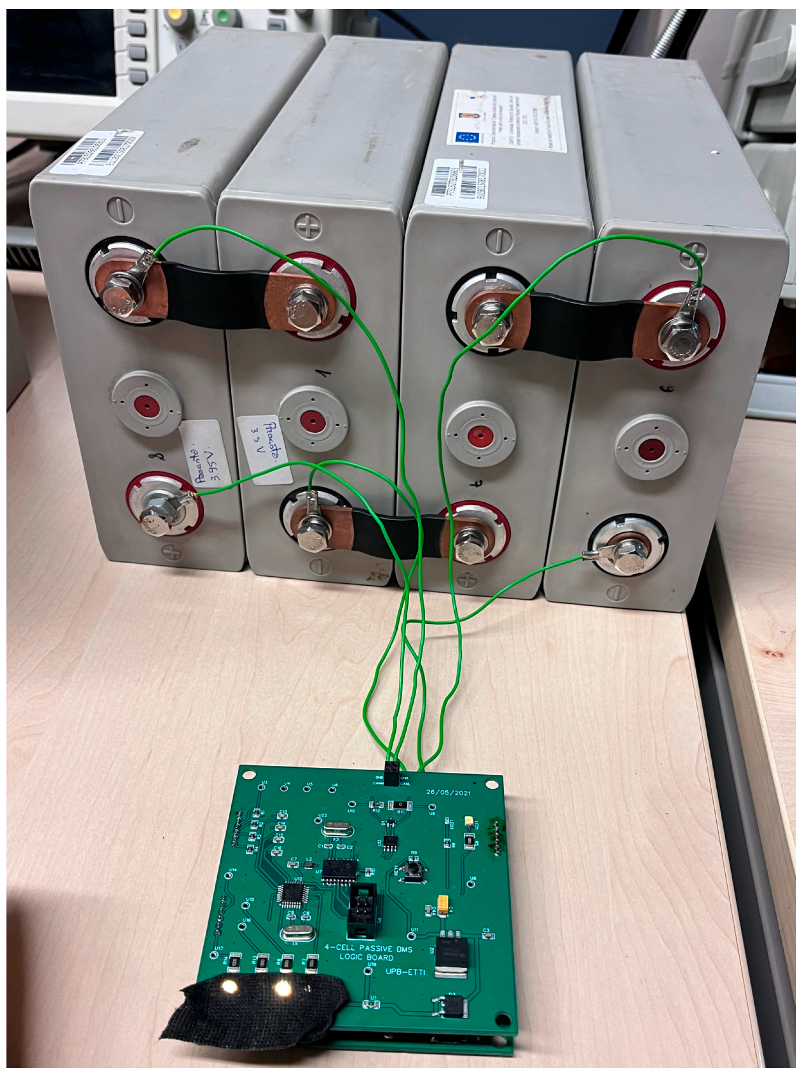
This paper proposes the design and implementation of a passive BMS that achieves the balancing of a four automotive-grade LiFePO4 cells connected in series. The cell equalizing is performed for both charging and discharging processes. The block diagram of the proposed BMS is visualized in Figure 2. There is one cell-balancing circuit and one voltage monitoring circuit for each cell in the battery pack. The cell voltages are acquired by the microcontroller, which also controls the balancing circuits. The acquired voltages are sent for remote monitoring over the CAN interface. The 7 V power supply circuit is used to power the balancing and voltage monitoring circuits, while the 5 V power supply circuit is used to power the microcontroller and the CAN interface.

2.1. LiFePO4 Cell

The LiFePO4 cell used in this design is the CA180FA from China Aviation Lithium Battery Limited (CALB) which is a high-power, high-quality LiFePO4 cell used for HEVs and EVs. Its specifications and operating conditions are detailed in Table 1 [26,27].
The OCV = f(SOC) characteristic of the CA180FA cell is presented in Figure 3. It can be noted that the OCV = f(SOC) is a highly non-linear function: between 10% and 90% SOC, the OCV varies in the range of 0.2 V, from around 3.15 V up to 3.35 V; outside the 10–90% SOC range, the characteristic varies abruptly towards the end cut-off voltages: 2.5 V for 0% SOC and 3.65 V for 100% SOC.

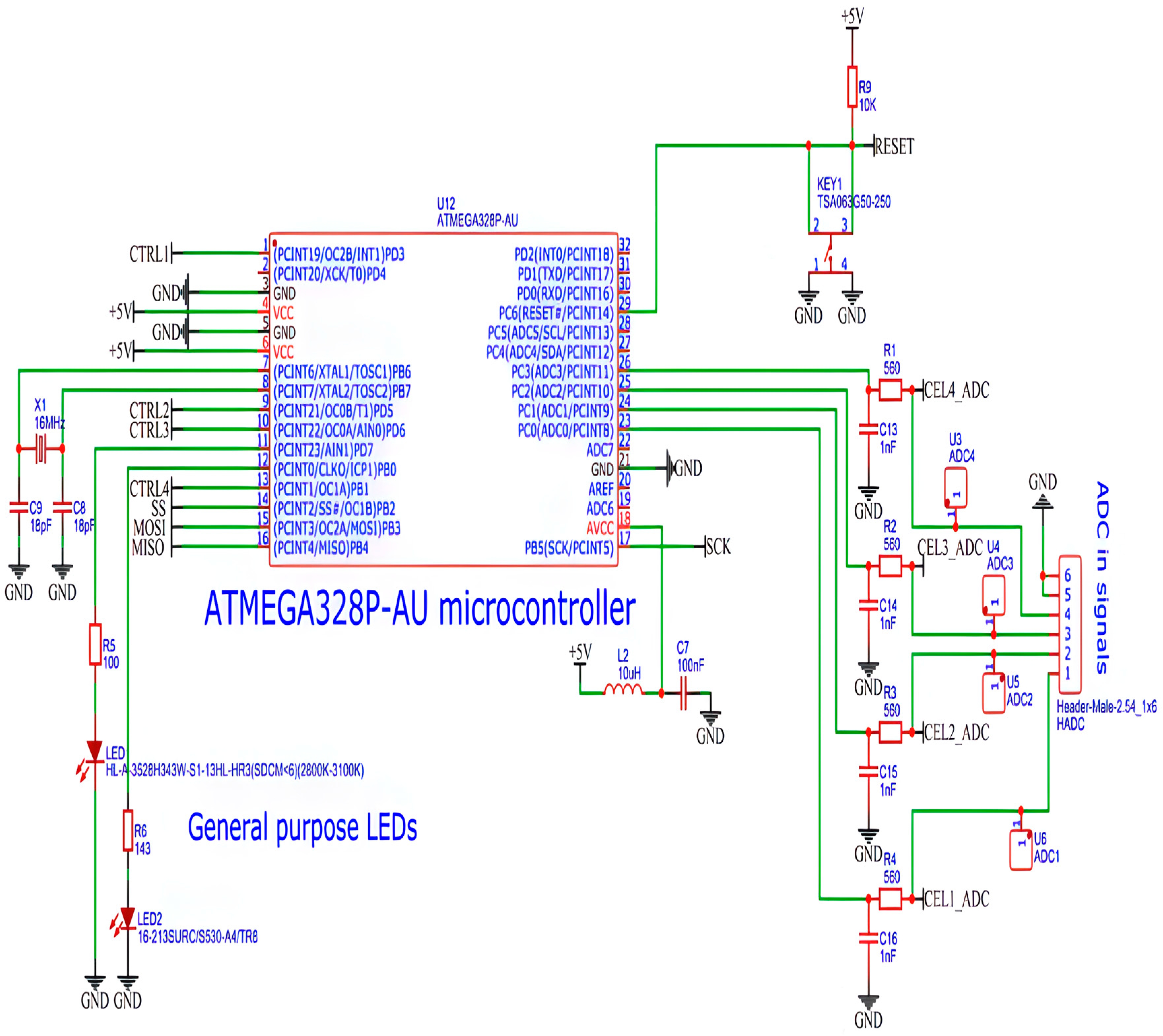
2.2. Cell Voltage Monitoring Circuit

The cell voltage monitoring circuit’s main function is to output a single-ended voltage (referenced to the BMS ground) based on the differential voltage coming from each cell’s “+” and “−” terminals. Essentially, the cell voltage monitoring circuit behaves as a difference amplifier.
The schematic of the cell voltage monitoring circuit is presented in Figure 4. The input ports CEL+ and CEL− represent the cell’s “+” and “−” terminals, while the output port CELL_VOLTAGE represents the difference in the voltages on CEL+ and CEL−. The circuit is powered by a 7 V voltage source referenced to the BMS ground GND. The circuit is based on the INA149AIDR (U1) high common-mode voltage difference amplifier from Texas Instruments. This is a precision unity gain difference amplifier that can accurately measure small differential voltages for common-mode voltages ranging from −275 V up to 275 V. The input differential voltage for a single-ended supply of 7 V can be in the range of 1.5 V–5.5 V, which includes the 2.5 V–3.65 V range of the LiFePO4 cell.
The AEC-Q100 Grade 1 automotive standard specifies that the junction temperature range must include the range of −40–125 °C. Since the INA149AIDR supports a temperature interval between −55 and 150 °C, it can be safely used in the automotive domain [28].
The internal schematic of IN149AIDR can be visualized in Figure 5, where the precision operational amplifier and the integrated thin-film resistor network can be observed [28].

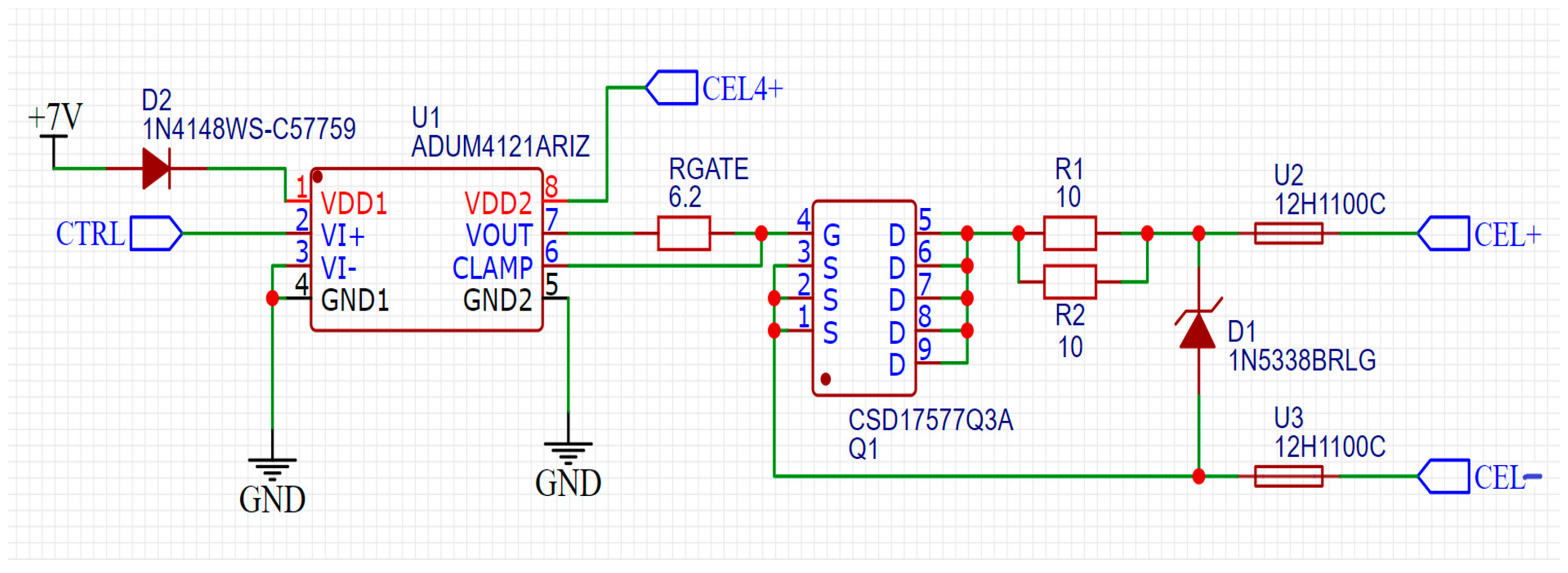
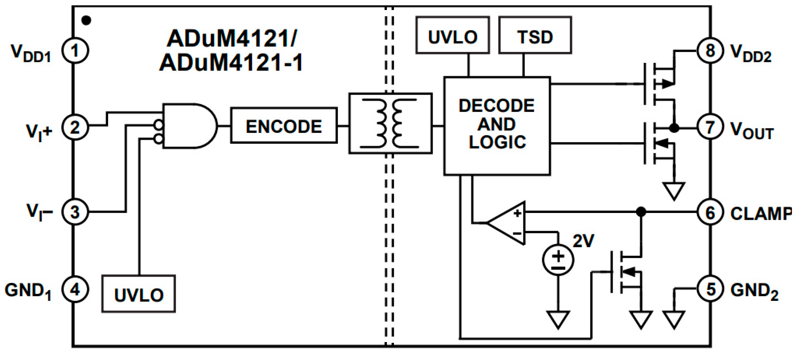
2.3. Cell-Balancing Circuit

The schematic of the cell-balancing circuit can be found in Figure 6. CEL+ and CEL− represent the two ports where each LiFePO4 cell is connected; CEL4+ represents the port where the fourth cell of the four-pack battery is connected, in order to supply the secondary side of the ADUM4121ARIZ gate driver (U1); while GND represents the BMS ground terminal connection. CTRL is the active high-control pin, which turns on the balancing process, while the primary side of the U1 gate driver is supplied from the 7V power source.
The main components of the cell-balancing circuit are the ADUM4121ARIZ gate driver (U1) and the CSD15577Q3A (Q1) N-channel power MOSFET.
ADUM4121ARIZ is a high-voltage, isolated gate driver with internal Miller clamping. It can be successfully used in the automotive domain due to its operating temperature range of −40 °C to 150 °C [29]. The functional block diagram can be found in Figure 7.
VDD1 represents the primary supply voltage pin and has an input voltage range between 2.5 V and 6.5 V; hence, the diode 1N4148WS-C57759 (D2) is used between the 7 V power supply and the VDD1 pin, such that the voltage on VDD1 is lower than 6.5 V. VI+ is the positive control pin, while VI− is the negative control pin. All of the primary side pins are referenced to the GND1 pin.
VDD2 represents the secondary-side power supply pin and has an input voltage range between 4.5 V and 35 V. VOUT is the gate driver output pin, which has the value of VDD2 when the gate driver is set into conduction and GND2 (which is the reference pin of the secondary side) when the gate driver is turned off. CLAMP represents the active Miller clamping pin, which sets into conduction an internal N-Metal–Oxide–Semiconductor Field-Effect Transistor (MOSFET) when the VOUT voltage becomes lower than 2 V during the off phase, reducing the hazard of parasitic turn-on.
The gate driver is turned on when the difference between VI+ and VI− becomes higher than 3.5 V, and it turns off when the difference between VI+ and VI− is lower than 0.3·VDD1. The gate driver also includes the Undervoltage-Lockout (UVLO) functionality, which halts the normal operation of the gate driver when the VDD1 voltage is lower than 2.35 V and when the VDD2 voltage is lower than 4.2 V.
ADUM4121ARIZ is used to set into conduction the CSD15577Q3A MOSFET (Q1). CSD15577Q3A is a NexFET™ power MOSFET from Texas Instruments designed to minimize the equivalent resistance in power conversion applications. It has a maximum VDS voltage of 30 V and a maximum VGS of 20 V, while the peak ID is 35 A. The typical threshold voltage Vth is 1.4 V. The 6.2Ω RGATE resistor has the role of limiting the VOUT signal slew rate controlling the gate G of Q1. The transistor Q1 is placed in series with the resistors R1 and R2, which are placed in parallel between the two of them [30]. D represents the transistor Q1’s drain, while S represents the transistor Q1’s source. When the gate driver U1 sets Q1 into conduction, the cell discharges through R1, R2, and Q1; hence, the RDSON of Q1 is very important for this application.
The RDSON vs. VGS characteristic is visualized in Figure 8. It can be noted that the characteristic remains lower than 20 mΩ at any VGS point; hence, the transistor RDSON can be neglected when compared with the 5Ω equivalent resistance of R1 and R2. Considering its RDSON and the voltage range of VGS and VDS, CSD15577Q3A is an excellent option in the automotive domain.
The 12H1100C, represented by U2 and U3, is a 1A safety fuse that has the role of cell protection in case the balancing current rises above 1 A. D1 1N5338BRLG is a Zener diode from ON Semiconductor with a maximum steady-state power dissipation of 5 W and an operating temperature range between −65 °C and 200 °C. The diode VZ has a minimum value of 4.85 V and a maximum value of 5.36 V, with a typical value of 5.1 V, at a current IZT of 240 mA [31]. The role of this diode is to protect the battery cell if its voltage accidentally increases over 5 V.
Since the equivalent resistance of R1, R2, and Q1 is approximately 5 Ω when Q1 is in conduction, this results in a theoretical balancing current varying between 0.5 A and 0.73 A when the cell voltage varies between its cut-off voltages of 2.5 V and 3.65 V.

2.4. Power Supply Circuit

The circuits that compose the passive BMS proposed in this paper are supplied by two single-ended voltages: 7 V for the voltage monitoring circuits and cell-balancing circuits, along with 5 V for the microcontroller and CAN interface.
The schematic view of the power supply circuit that produces 7 V at the output is presented in Figure 9. The circuit is a buck Direct Current–Direct Current (DC-DC) converter that is based on the LM5085-Q1 buck switching controller from Texas Instruments. LM5085-Q1 represents an automotive-grade product with an operating junction temperature ranging from −40 °C to 125 °C and is a high-efficiency P-Channel Metal–Oxide–Semiconductor (PMOS) switching regulator controller that can be used in an extended range of applications, such as automotive infotainment, battery applications, and Light-Emitting Diode (LED) drivers.
The chip operates based on the constant on-time regulation principle that does not require any loop compensation, hence resulting in a very fast load transient response. Its PMOS architecture allows for 100% duty cycle operation, and either the PMOS RDSON or an external resistor can be used to detect an overcurrent condition. Moreover, the controller has a wide input voltage range from 4.5 V up to 75 V, and the switching frequency can be programmed up to 1 MHz [32].
The VIN pin represents the input supply voltage and is connected to the total voltage produced by the four cells connected in series (CEL4+).
The RT pin is the on-time control and shutdown pin. If an external resistor is connected to VIN, then the on-time and switching frequencies are set. If RT is grounded, the controller is turned off. The on-time tON of the PMOS transistor is calculated as follows, and as given in the LM5085-Q1 datasheet [32]:
t O N = 50   n s + 1.45 · 10 7 · ( R T + 1.4 ) V I N 1.56 + R T 3167
where RT is the resistance value of R1 connected at the RT pin in kΩ, and VIN is the input voltage of the buck converter. The minimum on-time tON,min that occurs at the maximum input voltage VIN,max must be higher than 150 ns. For VIN,max = 4·3.65 V = 14.6 V and RT = 68 kΩ, tON,min becomes
t O N , m i n = 50   n s + 1.45 · 10 7 · ( 68 + 1.4 ) 14.6 1.56 + 68 3167 = 820   n s
The switching frequency FS is computed as follows [32]:
F S = V O U T · ( V I N 1.56 ) 1.45 · 10 7 · V I N · R T
For VOUT = 7 V, VIN = 12.8 V (the typical value of four series-connected LiFePO4 cells), and RT = 68 kΩ, FS becomes
F S = 7 · ( 12.8 1.56 ) 1.45 · 10 7 · 12.8 · 68 = 623   k H z
EP represents the exposed pad, and it must be soldered to the PCB ground plane (GND) in order to aid with the heat dissipation.
The VCC pin is the output of the negative voltage regulator (relative to VIN), and it biases the PMOS gate driver. A capacitor must be connected between VIN and VCC; in this case, C1 was chosen at 470 nF, providing a high surge current for the PMOS gate during each turn-on.
ADJ represents the current limit adjust pin. The current limit threshold is set using an external resistor between VIN and ADJ (RADJ1). In this case a sense resistor R2 of 0.01 Ω is used to measure the converter current; hence, the current limit threshold ILIMIT is calculated as follows [32]:
I L I M I T = 40   µ A · R A D J 1 R 2 = 40   µ A · 1.43   k 0.01   = 5.72   A
The CADJ1 capacitor of 1nF filters the noise at the ADJ pin and prevents the accidental switching of the current limit comparator due to input voltage transients.
The PGATE pin must be connected to the gate of the external PMOS Q1. In this case the PMOS transistor is FDD5614P from ON Semiconductor. FDD5614P is a 60 V P-Channel MOSFET with fast switching speed, extremely low RDSON (<100 mΩ), and high current capability (15 A). Its operating junction temperature range is −55 °C to 175 °C, making it suitable for the automotive domain. The usual applications are DC-DC converter power management and load switching [33].
D1 STPS20M100S-TR is a 100 V, 20 A, low-forward-voltage-drop power Schottky rectifier from STMicroelectronics that is suitable for high-frequency switch mode power supply. D1 creates a current path to GND for the inductor L1 when Q1 is turned off. The diode has a forward maximum current of 20 A, a maximum reverse voltage of 100 V, and a typical forward voltage of 0.61 A at around 10 A. D1 can be successfully used for temperature ranges between −40 °C and 150 °C, which are safe for automotive applications [34].
The inductor L1’s inductance value is calculated as follows [32]:
L 1 = t O N , m i n · ( V I N , m a x V O U T ) I r i p p l e , m a x
where Iripple,max is the maximum ripple current through inductor L1, chosen to be equal to 400 mA. For tON,min = 820 ns, VIN,max = 14.6 V, VOUT = 7 V, and Iripple,max = 400 mA, the L1 value becomes
L 1 = 820   n s · ( 14.6   V 7   V ) 400   m A = 15.58   µ H
hence, a standard value of 15µH is chosen for L1.
The ISEN pin represents the current sense input for the current limit detection. Here, an external sense resistor of 0.01 Ω (R2) is used.
FB is the voltage feedback pin coming from the regulated output 7 V_TP. The regulation level is 1.25 V, with a precision of ±2%. Based on this, the theoretical output voltage is calculated as follows:
V O U T = 1.25   V · R 3 + R 4 + R 5 + R 6 R 4 + R 5 + R 6 = 1.25   V · 12.183   k 2.183   k = 6.976   V
where R3, R4, R5, and R6 are the feedback loop resistance values.
The output capacitor C4’s capacitance value is as follows [32]:
C O U T = I r i p p l e , m a x 8 · F S · V r i p p l e
where Vripple represents the output voltage ripple. For Iripple,max = 400 mA, FS = 623 kΩ, and Vripple = 1 mV, COUT becomes
C O U T = 400   m A 8 · 623   k H z · V r i p p l e = 80.25   µ F
hence, a standard value of 68 µF is chosen.
The power supply schematic needed for the microcontroller and the CAN interface is presented in Figure 10. The 5 V power supply voltage is obtained by using the LM7805S Low-Dropout (LDO) regulator (U2), which is supplied by the 7 V output voltage produced by the buck converter.
LM7805S is a Low-Dropout voltage regulator from Texas Instruments that produces a 5V fixed output voltage. The output current capability is 1.5 A, but if adequate heatsinking is used, the chip is able to provide a current over 1.5 A. The regulator has three terminals: VCC represents the input voltage, OUT is the output voltage, while GND is the ground-point terminal. The allowed junction temperature can vary between −75 °C and 150 °C. The output voltage tolerance is ±2% at a junction temperature of 25 °C, the load regulation is 0.3%, and the line regulation is 0.01%. All of these characteristics make this chip suitable for use in the automotive domain [35].
The capacitor C3 has the role of rejecting the input voltage noise, while the capacitor C4A rejects the output voltage high-frequency noise. To be able to regulate the output voltage, a 10 µF capacitor is also used at the output (C4).
The 12H1100C, represented by U1, is a 1 A safety fuse described in detail in Section 2.3 and has the role of disconnecting the 7 V input voltage from the LDO regulator in case the current rises above 1 A, as a protection feature.
The diode D3 (MBRD360T4G) is a Schottky barrier rectifier from ON Semiconductor that has a reverse protection role in case the input voltage to the Low-Dropout (LDO) regulator is connected wrongly. The maximum value of the average rectified forward current is 3 A, while the forward voltage varies between 0.45 V and 0.7 V depending on the junction temperature, which can vary between −65 °C and 150 °C at its turn, making this diode suitable for the proposed BMS application [36].

2.5. Microcontroller Circuit

The proposed microcontroller circuit is shown in Figure 11. Its main functions are the acquisition of the voltages of the four cells connected in series, control of the cell-balancing circuits based on a specific equalizing algorithm, and control of the CAN interface for remote monitoring of the cell voltages. The BMS logic core is based on the ATMEGA328P-AU microcontroller provided by Microchip, which is a high-performance, low-power, 8-bit microcontroller. The ATMEGA328P-AU is AEC-Q100 grade-1-qualified and can be used successfully in the automotive domain, having a temperature range between −40 °C and 125 °C [37].
The used ATMEGA328P-AU microcontroller comes in a Thin Quad Flat Pack (TQFP) package with 32 pins. It uses a 16MHz clock signal provided by the X1 crystal oscillator, which has both of its terminals coupled to the ground through the 18pF capacitors C8 and C9.
The digital voltage VCC is provided by the 5 V LDO regulator (pins 4 and 6). The supply voltage for the Analog-to-Digital Converter (ADC) (AVCC, pin 18) is also provided by the 5 V regulator through the LC low-pass filter formed by L2 (10 µH) and C7 (100 nF). The reset functionality (pin 29) is connected to 5 V through a 10 kΩ pull-up resistor, which enables the normal operation of the microcontroller. The reset pin is also connected to the ground through the pushbutton KEY1, meaning that when the button is pushed, the reset is pulled to the ground, and the microcontroller operation is restarted. The microcontroller’s ground (GND) is connected to the first cell (cell 1)’s negative terminal in the final BMS circuit.
The voltages of the four series-connected cells are acquired by the microcontroller through the HADC six-pin male header using a 10-bit ADC. The header pins 5 and 6 are connected to GND, while pins 1–4 represent the actual cell voltages, named CEL1_ADC, CEL2_ADC, CEL3_ADC, and CEL4_ADC. These cell voltages are connected to the microcontroller’s ADC channels PC0, PC1, PC2, and PC3 (corresponding to microcontroller pins 23–26) through low-pass filters in order to eliminate the high-frequency noise. The low-pass filters are defined by the pairs R1-C13, R2-C14, R3-C15, and R14-C16, where each resistor is 560 Ω and each capacitor is 1 nF. The ATMEGA328P-AU 10-bit ADC has a resolution RESADC, calculated as follows:
R E S A D C = A V C C 2 10 = 5 V 1024 = 4.883   m V
where AVCC is the ADV supply voltage pin tied at 5 V.
The control signals that command the cell-balancing circuits are given by the CTRL1, CTRL2, CTRL3, and CTRL4 nets, where CTRLx corresponds to the cell-balancing circuit for cell x. CTRL1 is connected to the microcontroller PD3 pin, CTRL2 to PD5, CTRL3 to PD6, and CTRL4 to PB1; hence, the Port D data register and Port B data register will be used for the control signals.
There are two general-purpose LEDs (LED1 and LED2) that can be configured by the user based on their preference. LED1 is connected to PD7 through a 100 Ω resistor (R5), while LED2 is connected to PB0 through a 143 Ω resistor (R6).
The CAN interface is controlled through the Serial Peripheral Interface (SPI) interface using the SS, MOSI, MISO, and SCK signals. SS represents the slave select pin and is connected to the microcontroller PB2, MOSI represents the master-out slave-in pin and connects to PB3, MISO is the master-in slave-out pin and is connected to PB4, while SCK (serial clock pin) is connected to PB5. The data transmitted by the ATMEGA328P-AU microcontroller over SPI has a length of 1 byte (8 bits); hence, in order to transmit the 10-bit ADC result, two SPI data transmissions are needed.

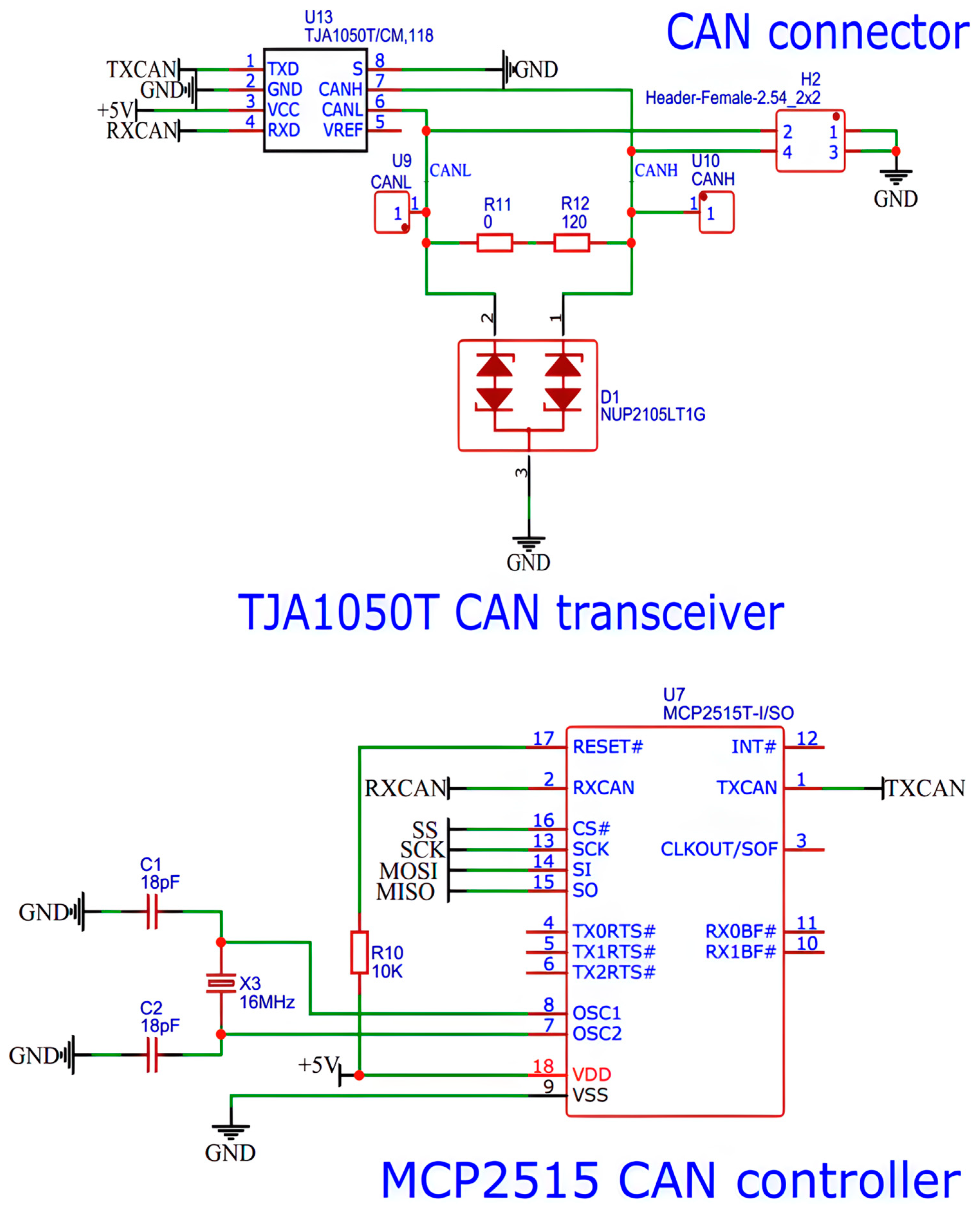
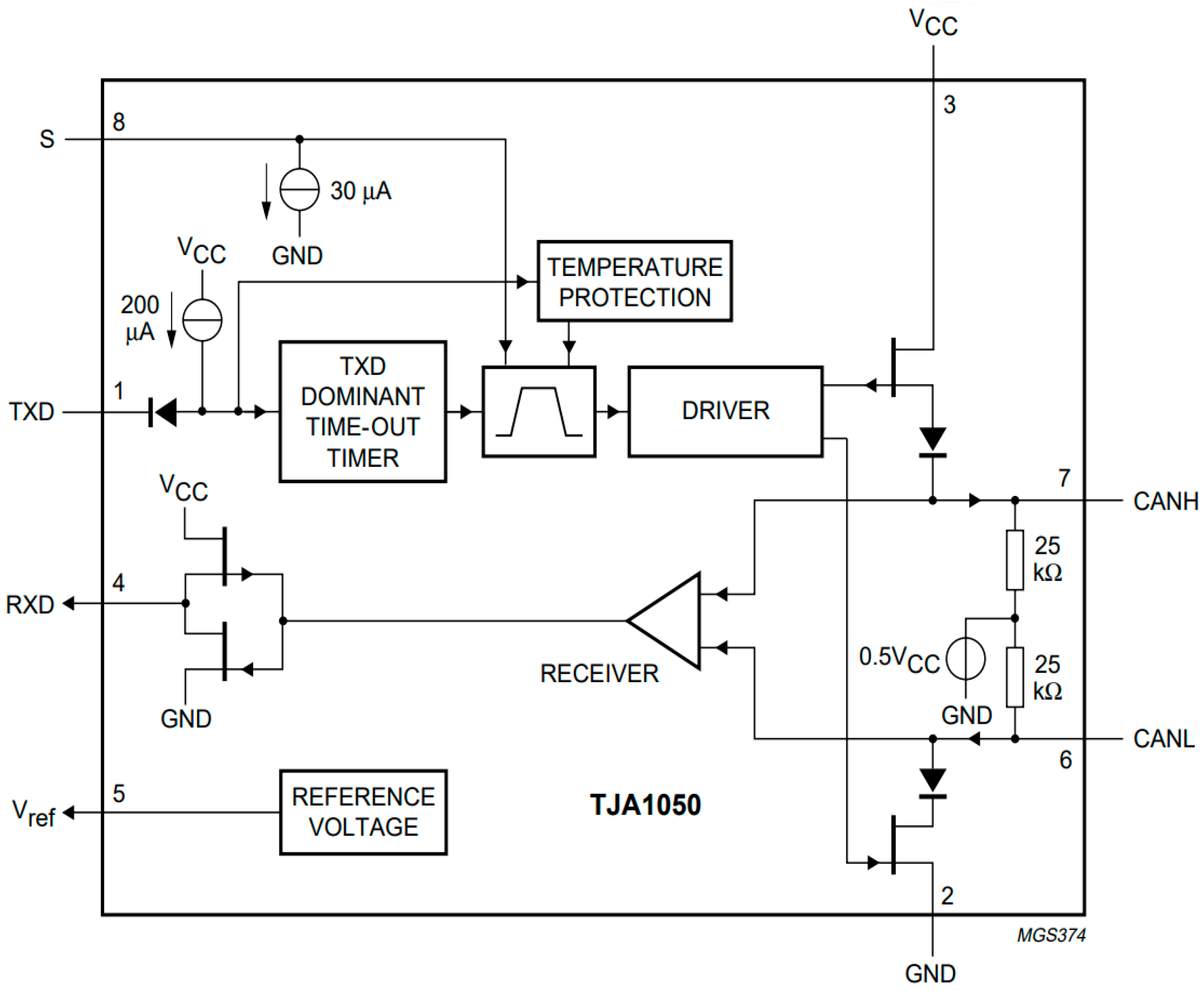
2.6. CAN Interface Circuit

The remote monitoring of the four-cell pack is performed through the transmission of the cell voltages over the CAN interface. The CAN interface circuit is presented in Figure 12 and has two main components: the MCP2515 CAN controller (U7) and the TJA1050T CAN transceiver (U13).
MCP2515, provided by Microchip Technology, is a standalone CAN controller that is interfaced with a microcontroller through an industry-standard SPI. It can transmit and receive both standard and extended CAN data frames. The controller is based on low-power Complementary Metal–Oxide–Semiconductor (CMOS) technology, operates at supply voltages between 2.7 V and 5.5 V, has a typical 5 mA active current and 1 µA standby current in sleep mode, and also supports a temperature range between −40 °C and 125 °C, making it an excellent choice in the automotive domain [38].
The MCP2515 block diagram is shown in Figure 13. The CAN module is formed by the CAN protocol engine and the masks and filters for the transmit (TX) and receive (RX) buffers. The CAN module handles all of the functions needed to transmit and receive messages on the CAN bus. The transmission is initiated by the use of control registers’ bits through the SPI, or by the use of the transmit-enable pins ( T X 0 R T S ¯ , T X 1 R T S ¯ , T X 2 R T S ¯ ) [38].
The control logic block interfaces with the other blocks in order to control the operation of MCP2515. The general-purpose interrupt pin ( I N T ¯ ) can be used when valid messages are received. The specific interrupt pins ( R X 0 B F ¯ , R X 1 B F ¯ ) indicate when a valid message was received and loaded in the receive buffers [38].
The SPI logic is used to interface with the host microcontroller. Standard SPI write and read commands can be used to write to all registers and to read from all of the registers [38].
TXCAN represents the transmit output pin to the CAN bus, while RXCAN represents the receive input pin from the CAN bus. CLKOUT is the clock output pin with a programmable prescaler, but it also has an alternate function as the start-of-frame signal. The crystal oscillator is connected between pins OSC1 and OCS2 [38].
For the proposed BMS, the MCP2515 CAN controller operates at a clock frequency of 16 MHz given by the X3 crystal oscillator coupled to the ground via 18 pF capacitors, C1 and C2. The chip is supplied with a VDD voltage of 5 V provided by the LDO regulator. For this system, the microcontroller has full control of MCP2515 via the SPI; the other interrupt and control pins ( T X 0 R T S ¯ , T X 1 R T S ¯ , T X 2 R T S ¯ , I N T ¯ , R X 0 B F ¯ , R X 1 B F ¯ ) are not used and are left disconnected.
TJA1050T is a high-speed CAN transceiver manufactured by Philips Semiconductors and acts as the interface between the MCP2515 CAN controller and the physical CAN bus. This device is able to provide differential transmission capability towards the CAN bus and differential reception capability towards the CAN controller. TJA1050T offers speeds of up to 1Mbaud, and it has very low electromagnetic emissions and a silent mode in which the transmitter is disabled. The junction temperature interval is from −40 °C up to 150 °C. Moreover, the chip is compatible with both 3.3 V and 5 V devices, has short-circuit protection to the battery and ground sides, and the bus pins are protected against transients in automotive applications. A minimum of 110 nodes can be connected to the CAN transceiver [39].
The TJA1050T block diagram is presented in Figure 14. VCC represents the supply voltage, which is the 5 V provided by the LDO regulator, while GND is the transceiver’s ground point, connected to the global BMS ground, represented by the cell 1 negative terminal. TXD is the transmit data input and contains the data coming from the CAN controller to the bus line drivers, being pulled up to VCC via a 200 µA current source. RXD is the receive data output and forwards data from the bus lines towards the CAN controller. Vref represents the reference voltage output, and it is typically 0.5·VCC. CANL is the low-level CAN bus line, while CANH is the high-level CAN bus line. S represents the select input for normal operation mode or silent mode [39].
The normal operation mode is chosen by connecting the S pin to the ground. If S is left floating, it is automatically pulled to the ground by the 30 µA current source. If S is connected to VCC, the silent mode is selected, where the transmitter is disabled, but all of the other functions continue to work. The silent mode can also be used to prevent network communication from becoming stuck due to CAN controller malfunction [39].
The TXD dominant time-out timer prevents the bus lines from becoming stuck in a permanent dominant state (CANH-CANL = high) when TXD is forced low by either software or hardware malfunctions. The timer is started by a negative edge on TXD and reset by a positive edge on TXD. If the low duration of TXD is higher than the timer value, the transmitter is disabled and the bus is driven into a recessive state (CANH-CANL = low) [39].
The resistors R11 (0 Ω) and R12 (120 Ω) in Figure 12 represent the termination resistors of the CAN network connected between the CANH and CANL terminals. They are needed due to the fact that the majority of the wiring used in CAN networks has a characteristic impedance of 120 Ω.
D1, represented by NUP2105LT1G in Figure 13, is a dual bidirectional voltage suppressor manufactured by ON Semiconductor, designed to protect the CAN transceiver from Electrostatic Discharge (ESD) and other voltage transient events that may cause harm to the transceiver. This voltage connects between the CANH and CANL terminals and represents a low-cost option that improves the system’s reliability, having a peak power dissipation of 350 W per line [40]. It can be successfully used in the automotive domain for both low- and high-speed CAN networks.

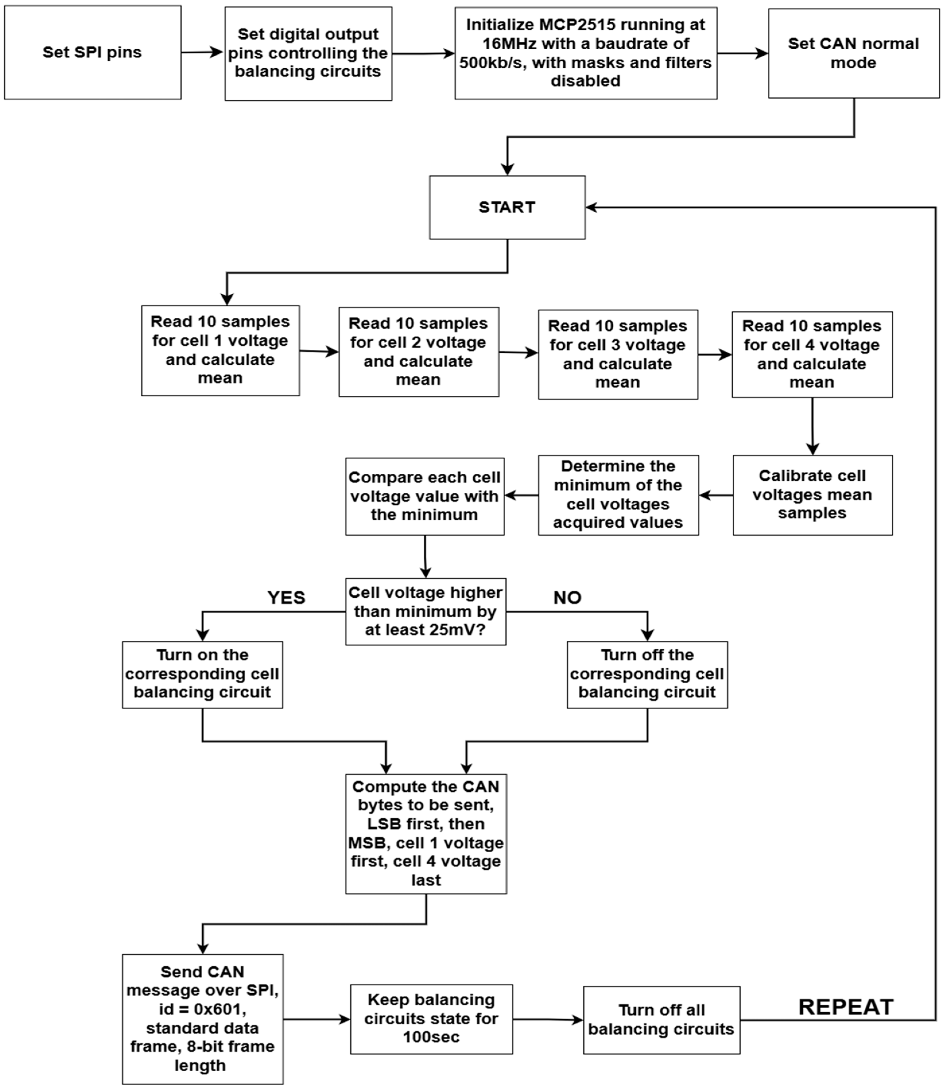
2.7. Software Implementation

The software part of the proposed BMS consists of the C code uploaded into the ATMEGA328P-AU microcontroller, which performs the following tasks: voltage measurement of each individual cell in the battery pack, control of each individual balancing circuit, and transmission of the cell voltages over the CAN interface for remote monitoring.
The software flowchart of the proposed passive BMS with remote monitoring is visualized in Figure 15.
Once the microcontroller is powered for the first time, the initial setup is complete. The first step is to initialize and set the SPI pins, and afterwards, the pins controlling the balancing circuits are set as output pins. The next step is to set the CAN speed of MCP2515 at 500 kbps and its clock signal at 16 MHz given by the crystal oscillator. The CAN’s normal operating mode is asserted.
After this initial setup, the microcontroller loop is started. For each cell voltage, 10 samples are acquired, and then the average value is computed. In this way, wrong readings of the ADC are eliminated. The final average values of the acquired voltages are then calibrated by introducing an offset in the software code, based on laboratory measurements of the real cell voltages.
Once the cell voltages are acquired and calibrated, the minimum value amongst them is determined. After this step, each cell voltage is compared with the minimum value. If the current cell voltage that is compared is at least 25 mV higher than the minimum, the corresponding cell-balancing circuit is activated.
The CAN transmission algorithm begins by computing the data that need to be sent to the MCP2515 CAN controller. Since the ATMEGA328P-AU ADC is on 10 bits and the data sent over the SPI have 8 bits, two 8-bit data frames are needed for each cell voltage. The cell voltages’ first 8 least-significant bits are sent first, followed by the most significant 8 bits. The transmission order is from cell 1 to cell 4. After the CAN transmission of the cell voltages ends, the cell-balancing circuits keep their on/off state for 100 s. After the 100 s has elapsed, the cell-balancing circuits are turned off in order to begin a new cycle of cell voltage acquisition. The cell voltages’ acquisition cannot be performed with the balancing circuits turned on, because the current flowing through the connection wires introduces measurements errors.

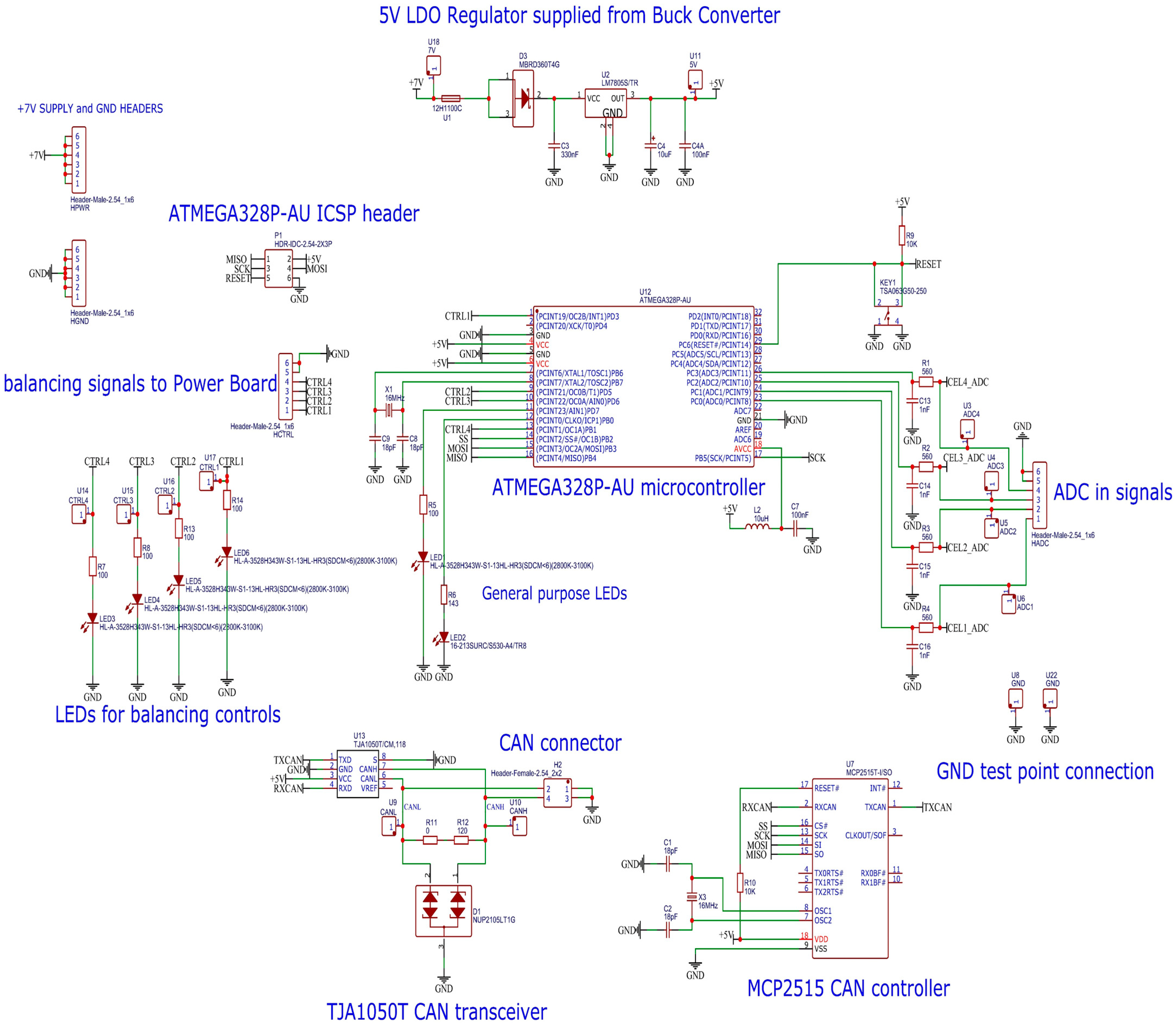
2.8. Full Schematic of the Proposed Battery Management System

The full schematic of the proposed passive BMS is presented in Figure 16 and Figure 17. The BMS design is split into two parts, depending on the predominant logic: analog or digital. Each schematic is translated into one PCB, and they are merged together but can also be tested separately.
Figure 16 shows the BMS schematic of the analog part, containing the buck converter, the four voltage monitoring circuits, and the four cell-balancing circuits.
Figure 17 shows the BMS schematic of the digital part and includes the ATMEGA328P-AU microcontroller, with the low-pass filter for the cell voltage acquisition, the general-purpose LEDs (LED1 and LED3), and the LEDs that turn on when the corresponding cell-balancing circuit is activated (LED3, LED4, LED5, and LED6). The circuits needed for the CAN remote monitoring, MCP2515 and TJA1050T, are also found in the schematic. Moreover, the 5 V LDO regulator is also found in this schematic, as it supplies all of the digital part.

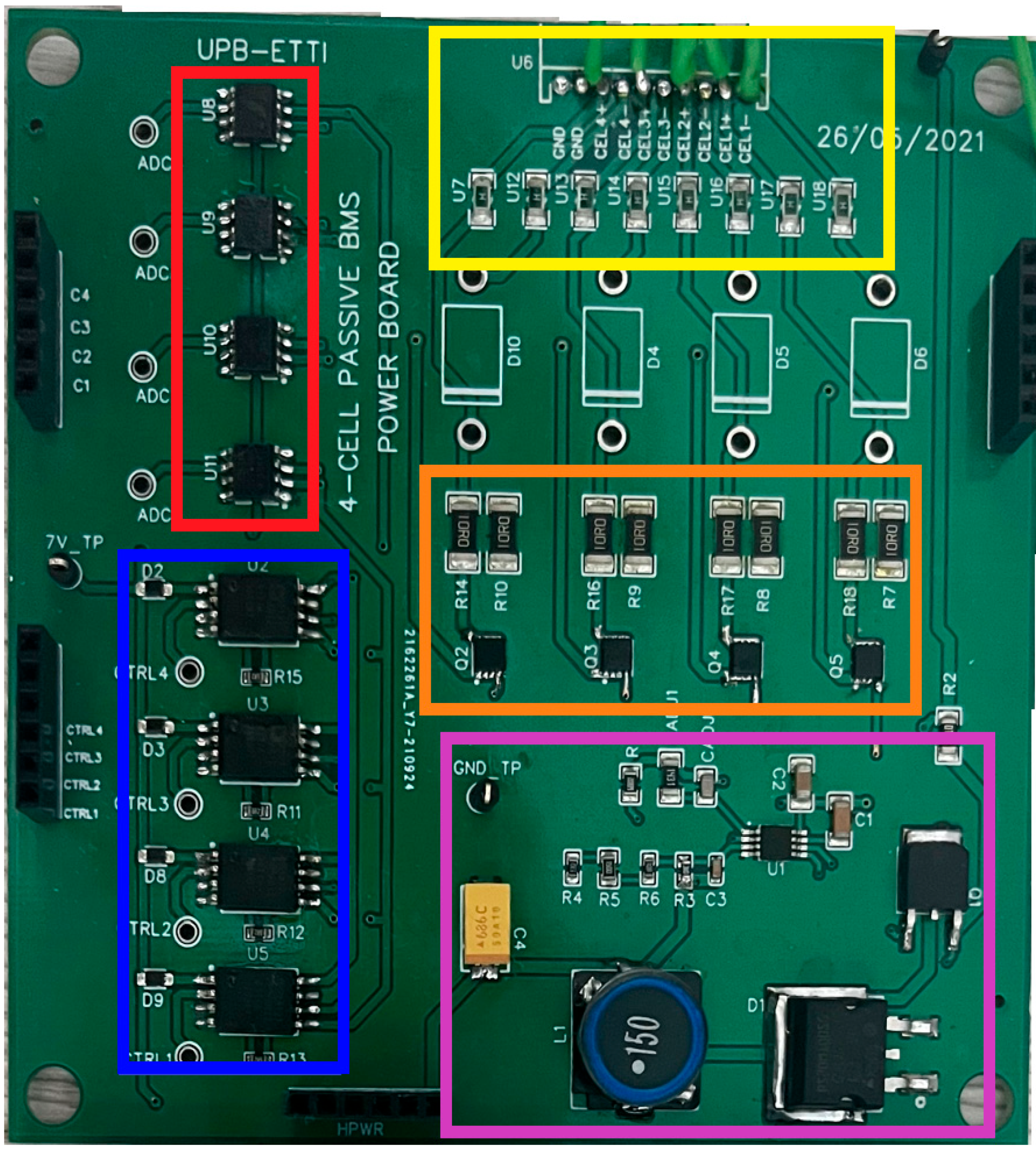
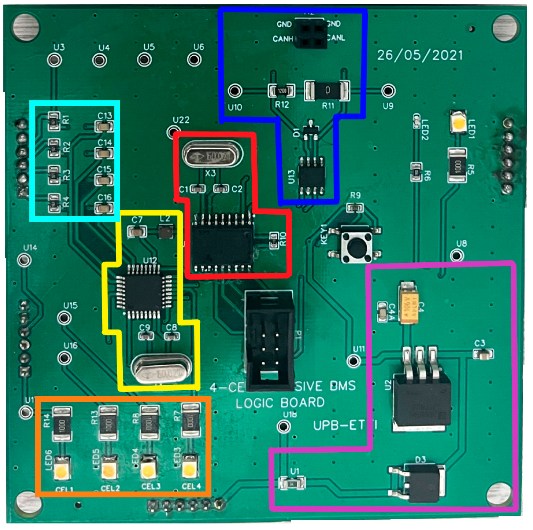
2.9. Printed Circuit Boards of the Proposed Battery Management System
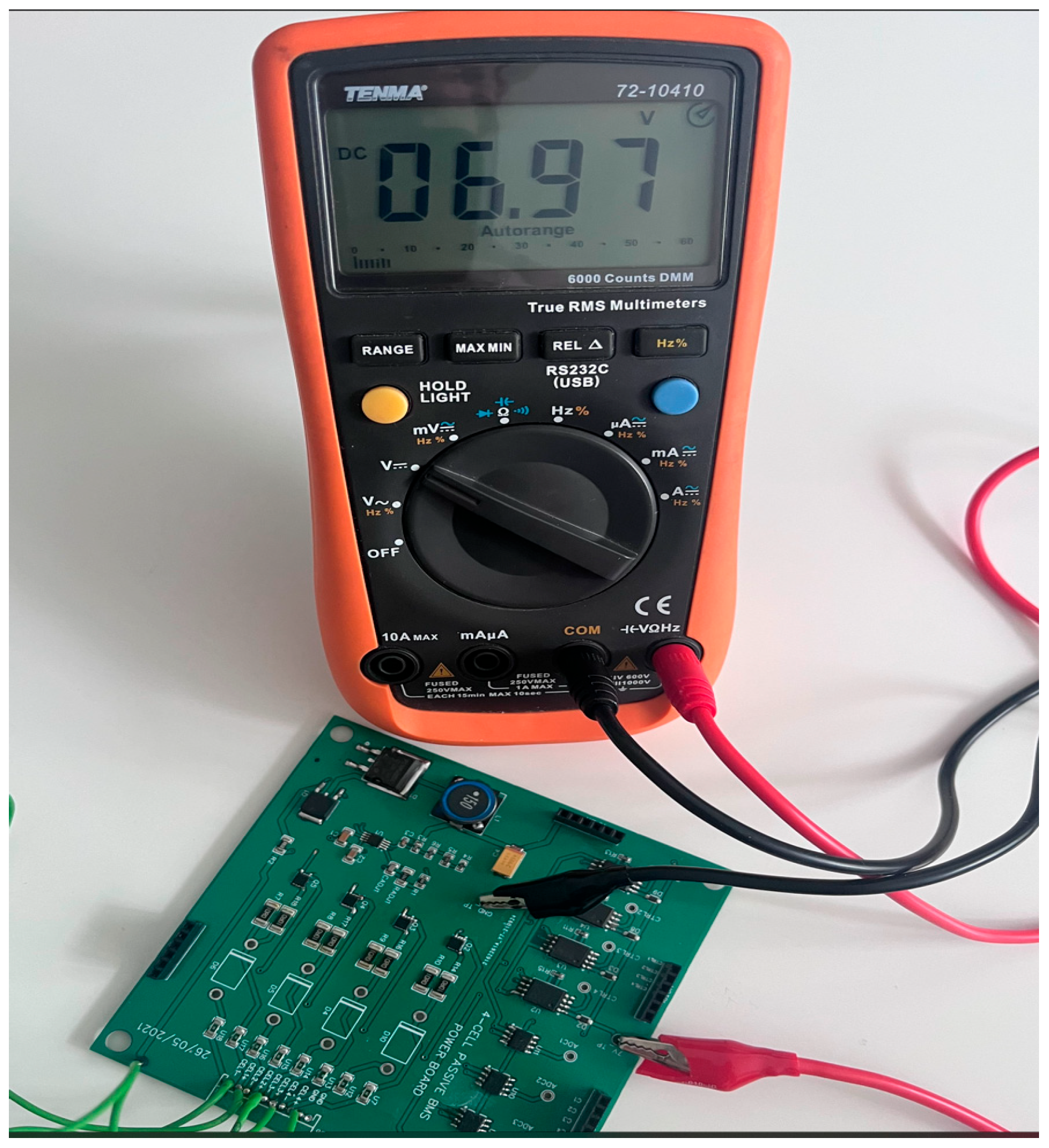
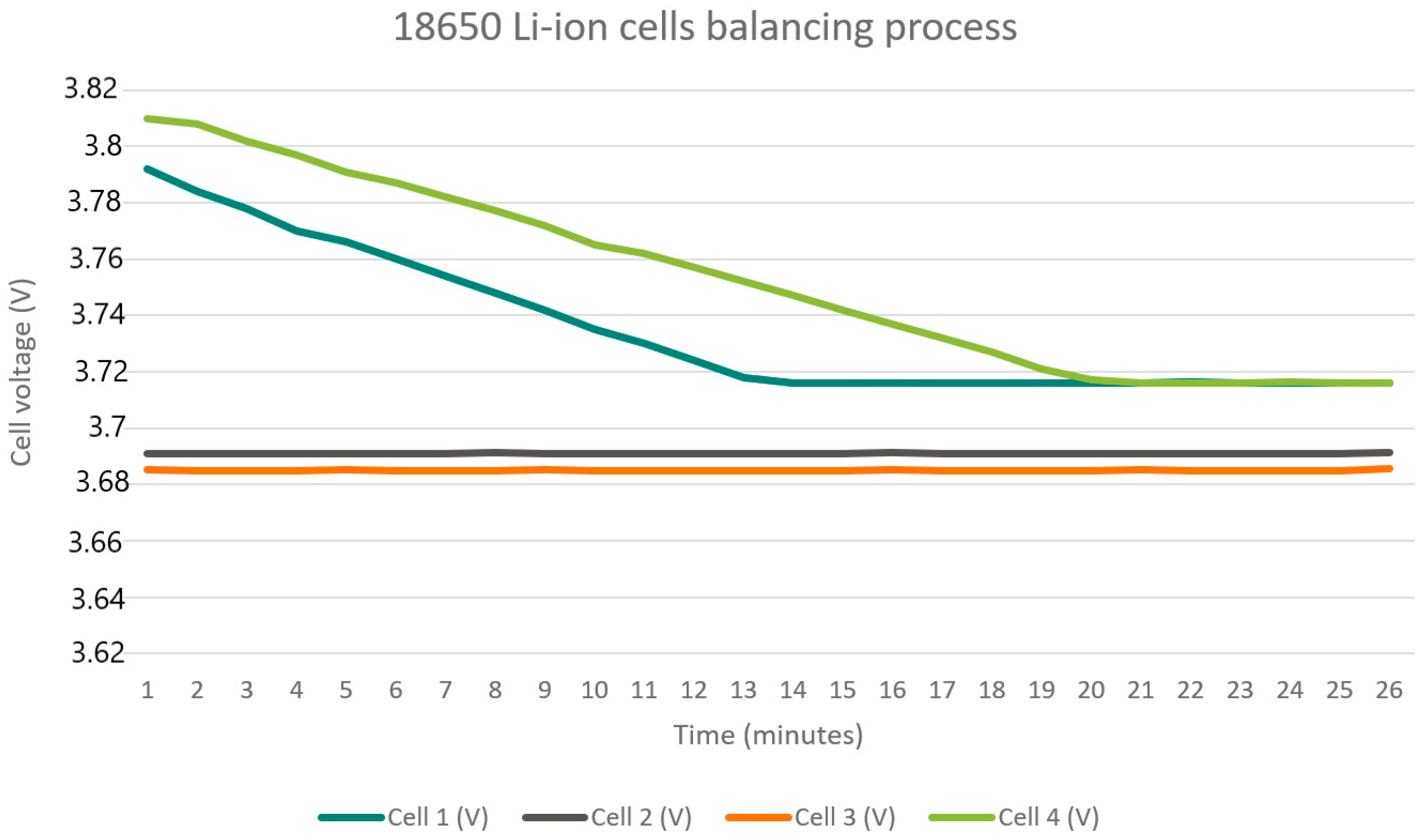
The proposed BMS is composed of two PCBs that are interconnected. The first PCB contains the analog circuitry and the supply voltage for the analog circuits, such as the buck converter, cell-balancing circuits, and cell voltage monitoring circuits. The second PCB contains the digital circuitry and the supply voltage circuit for the digital part, such as the LDO regulator, ATMEGA328P-AU microcontroller, MCP2515 CAN controller, and TJA1050T CAN transceiver. The two-PCB implementation was chosen due to the fact that each PCB can also be tested separately in order to speed up the verification stage.
The analog circuitry PCB is presented in Figure 18. The LiFePO4 cells are connected to the board in the top part, highlighted in yellow, while the cell voltage monitoring circuits are found in the top left part of the board, in the red box. The cell-balancing circuits are composed of the gate drivers, highlighted in blue, along with the power resistors and the power transistors in the orange bounding box. The buck converter is found in the bottom right part of the PCB, encircled in purple.
The digital circuitry PCB is shown in Figure 19. The ATMEGA328P-AU microcontroller IC, along with its crystal oscillator, is highlighted in yellow; the low-pass filters that connect the outputs of the voltage monitoring circuits to the microcontroller ADC inputs are encapsulated in the light blue box; while the LEDs that signal the activation of the cell-balancing circuits are emphasized in the orange bounding box. The LDO voltage regulator circuit is highlighted in purple, the MCP2515 CAN controller IC with the other external components is encircled in red, and the TJA1050T CAN transceiver is encapsulated in a dark blue box. The software code is uploaded onto the microcontroller using the six-pin ICSP header found in the middle of the PCB.

3. Results

The first verification setup containing the CA180FA LiFePO4 cell is presented in Figure 20. As can be seen, the digital circuitry PCB is placed on top of the analog circuitry PCB, connected by header pins, and in this way the proposed BMS is obtained. The final BMS is then connected by wires to the LiFePO4 cells placed in series. There is no external load attached to the LiFePO4 pack.
The output voltage produced by the buck converter is shown in Figure 21. The measured output voltage is 6.97 V, while the calculated theoretical output voltage is 6.976 V, which results in a relative error of 0.086%. Thus, the designed 7 V buck converter works as expected.
The output voltage produced by the LDO regulator can be seen in Figure 22. The measured LDO output voltage is 5.009 V, while the theoretical output voltage is 5 V, which results in a relative error of 0.18%, thus showing the correct operation of the LDO regulator.
The first step to perform is the software calibration in order to remove the error propagated through the voltage monitoring circuits, which are influenced by offset voltages and the wires used to connect the BMS to the battery cells.
The measurements performed for the software calibration of the LiFePO4 cells are shown in Table 2.
Table 3 presents the actual voltages of the LiFePO4 cells measured using a multimeter, along with the cell voltages acquired by the microcontroller and the relative errors of the acquired voltages, with measurement points taken throughout the balancing process. The relative cell voltage measurement error varies between 0.03% and 0.12%, which is considerably lower than the initial error range of 0.4–1.23% that was obtained without introducing the software calibration.
The next step after the software calibration in the verification process is the testing of the balancing circuits of the BMS. It can be noted that the LEDs corresponding to the cell-balancing circuits 1 and 3 are turned on; hence, based on the equalizing algorithm, only the cells that are at least 25 mV higher than the minimum value (given by the cell 2 voltage, 3.284 V) are balanced. The theoretical and measured balancing currents for cells 1 and 3 can be found in Table 4. In this table, cells 2 and 4 are missing, because they do not fulfill the balancing condition, which requires the cell voltage to be at least 25 mV higher than the minimum cell voltage of 3.284 V. The measurements are performed at the voltage points shown in Table 2 and Table 3. It can be noted that the relative errors of the measured current versus the theoretical current are 0.95% and 1.23%, respectively. This is given by the resistance of the bonding wires, but it is still very low, another characteristic of a high-performance BMS.
Figure 23 shows the LiFePO4 cell voltages during their balancing process. It can be noted that the voltages of cells 2 and 4 remain constant, as they do not meet the balancing condition (cell voltage higher than the minimum by at least 25 mV), while cells 1 and 3 decrease towards cells 2 and 4, with the balancing process being completed in 36 h. These results show that the BMS performs the balancing task successfully.
In order to verify the BMS’s compatibility with another type of cell (Li-ion chemistry), another verification test bench was created, as shown in Figure 24. The cells used in this setup were 18650 Li-ion cells with a nominal capacity of 3000 mAh. A much lower capacity was chosen in order to achieve the cells’ balancing process in a shorter period of time. The nominal cell voltage is 3.7 V, while the minimum and maximum cut-off voltages are 3.0 V and 4.2 V, respectively [41]. No external load was connected to the four series-connected 18650 Li-ion cells.
Figure 25 shows the balancing process of the Li-ion cells over time. Cell 3 has the lowest cell voltage, and cell 2 is just 6 mV higher at the beginning of the balancing process; hence, they do not undergo balancing, having their corresponding balancing circuits turned off. It can be noted that cells 1 and 4 decrease towards the voltages of cells 2 and 3, with the balancing process being stopped when they become 25 mV higher than the minimum value after 13 min for cell 1 and 20 min for cell 4, concluding that the proposed passive BMS also works successfully for the Li-ion battery chemistry. The balancing currents at the beginning of the balancing process were 749.4 mA for cell 1 and 754.4 mA for cell 4.
In order to verify the CAN transmission of the cell voltages, the CANH and CANL terminals were connected differentially to the SIGLENT SDS 1104X-E oscilloscope, as shown in Figure 26.
The CAN transmission of the four cell voltages is presented in detail in Figure 27 and Figure 28. The CAN message contains the following fields, in this order: SOF (1 bit), identifier (11 bits), RTE (1 bit), IDE (1 bit), r0 (1 bit), DLC (4 bits), fata (8 bytes), CRC (16 bits), ACK (2 bits), EOF (7 bits), and IFS (3 bits).
SOF represents the start of the frame and marks the start of the CAN message being sent. The identifier is an 11-bit field establishing the priority of the message on the CAN bus. Here, the identifier is 0x601. RTR represents the remote transmission request and becomes dominant (CANH-CANL = HIGH) when the information is needed from another node. IDE stands for identifier extension and is dominant when a standard CAN message is transmitted. The single-bit field r0 is a reserved bit. DLC specifies the number of data bytes being transmitted—in this case, 8 bytes, because 2 bytes is needed for each cell voltage. After DLC, 64 bits (8 bytes) of data follows, representing the cell voltages. The CRC bit field represents the cyclic redundancy check and has 15 bits plus 1 delimiter bit. The ACK field has 2 bits; the first one is the acknowledgement bit, and the second one is the delimiter. When the message is error-free, the acknowledgement bit becomes dominant. The 7-bit EOF represents the end of the CAN message and disables the bit stuffing. The bit stuffing means that when 5 bits of the same logic level appears in a row, a bit of the opposite logic level is inserted into the data. The 3-bit IFS field shows the time needed by the controller to move an error-free received CAN frame to its proper position in a message buffer area [42].
The proposed BMS transmits the cell voltages successfully over the CAN interface, such that the user is able to monitor the battery pack remotely. The transmission uses standard CAN messages at a rate of 500 kpbs. The CAN transmission represents an essential characteristic of a modern BMS.

4. Discussion

In 2019, Nizam, Maghfiroh, et al. [43] proposed a passive BMS for three LiFePO4 cells connected in series, which was able to measure the cell voltages with a relative error varying between 0.367% and 0.535%, while the maximum balancing current was 200 mA.
In 2019, Xu, Jiang, and Zhang [44] designed a passive BMS for twelve Li-ion cells connected in series, which measured the cell voltages with an error between 0% and 0.166%, but there was no information given on the achievable balancing currents.
In 2022, Ramelan et al. [45] designed a BMS with passive balancing and multistage constant-current charging for four Li-ion cells connected in series. The voltage monitoring was performed with a relative error of 7.5%, while the balancing current had a maximum value of 150 mA.
In 2022, Canilang, Caliwag, and Lim [14] implemented a passive modular BMS for four Li-ion cells connected in series that measured the cell voltages with a relative error ranging between 0.028% and 0.051%, with a maximum balancing current of 110 mA.
The passive BMS proposed in this paper is able to achieve a cell voltage monitoring error ranging between 0.03% and 0.12%, which is lower than that of the above-mentioned [43,44,45] battery management systems, but slightly higher than the 0.051% error of [14]. However, the absolute voltage difference between an error of 0.051% and 0.12% is negligible. Moreover, the other BMSs can achieve balancing currents that do not exceed 200 mA, while the proposed system can reach balancing currents of up to 750 mA, which translates into an almost fourfold faster balancing time. In addition, none of the above-mentioned systems implement remote monitoring of the battery parameters, while the BMS presented in this paper includes the CAN transmission of the cell voltages.
The performance comparison is synthesized in Table 5 below.
Although the proposed system requires up to 36 h to complete full balancing of the LiFePO4 cells, this duration is consistent with the expected performance of passive balancing architectures, especially when high initial cell imbalances are present. In practical automotive applications, balancing usually occurs incrementally during repeated charging cycles, which mitigates the impact of the longer duration. Furthermore, the higher balancing current capacity of up to 750 mA in this design significantly reduces the time compared to traditional passive BMSs operating at 100–200 mA, helping to improve overall efficiency without increasing system complexity.
Despite its high performance metrics, the proposed system’s scalability to large battery configurations requires further consideration. As the number of cells increases, the power dissipation in passive balancing resistors can become excessive, potentially leading to thermal management challenges and reduced energy efficiency. This issue is especially relevant in large-scale electric vehicle battery packs, where dozens or hundreds of cells are used. While the simplicity and robustness of passive balancing make it a practical solution for small-to-medium battery packs, scaling it up without modifications may limit its applicability due to increased heat and power losses.
Moreover, the use of higher balancing currents, while beneficial in reducing the balancing time, could introduce long-term stress on the battery cells. Prolonged or repeated exposure to elevated currents may accelerate degradation mechanisms, including increased internal resistance and localized heating. Therefore, optimizing the balance between fast equalization and cell longevity is essential in future iterations of the design.
The proposed BMS employs a discrete, low-cost architecture that avoids complex integrated solutions while still supporting essential features like high-accuracy monitoring and CAN-based communication. The total cost of the BMS was 35 USD. This is significantly lower than that of commercial active BMS solutions, which can exceed 50 to 100 USD per unit, depending on features. Thus, the proposed design offers a favorable trade-off among cost, monitoring accuracy, and balancing performance for applications where affordability is a primary constraint.

5. Conclusions

This paper proposes the design and the practical implementation of a fast-balancing passive battery management system with remote monitoring that can be used in the automotive industry. The BMS was designed specifically for a battery formed of four series-connected CA180FA LiFePO4 cells, which were selected due to their high energy density.
The passive balancing technique was chosen for the proposed BMS because it is the most suitable technique for EVs and HEVs, employing simpler, smaller circuits with a less complex command-and-control strategy compared to the active balancing technique. The proposed BMS performs the cell balancing for both charging and discharging cycles, thus ensuring a shorter balancing time. This BMS is modularly designed, with four cell voltage monitoring circuits, one for each cell, as well as four cell-balancing circuits.
The verification results show that the cell balancing was performed successfully for the CA180FA LiFePO4 cells, with the cells being equalized in approximately 36 h. Moreover, the proposed BMS can also be successfully used with the Li-ion battery chemistry, equalizing a four-pack of 18650 Li-ion cells with 3000 mAh capacity in around 20 min.
The cell voltage monitoring was performed with a maximum relative error of maximum 0.12%, and the balancing current varied between 650 mA and 750 mA. While other similar approaches in the literature have managed to achieve a relative error of 0.051% for the cell voltage monitoring, which is similar to that of the proposed BMS, the balancing currents were limited to a maximum of 200 mA, thus proving again the enhanced performance of the new BMS. Moreover, the remote monitoring uses a standard CAN protocol at a data rate of 500 kpbs in order to transmit the four cell voltages over the CAN interface, such that the user knows the battery condition in real time. This characteristic is not approached in other similar passive BMS designs from the literature in this domain.
While the system was tested in a low-interference environment, typical CAN bus implementations exhibit low latency (often under 5 ms) and are inherently robust due to built-in error detection features such as cyclic redundancy checks (CRCs), automatic retransmission, and message prioritization. For deployment in high-noise automotive environments, the use of isolated transceivers and proper shielding would further enhance the communication reliability. Future work will explore these aspects in greater depth, including fault injection testing and validation under electromagnetic interference (EMI) conditions.
Another advantage of the proposed BMS is the modular design presented in this work, which allows for further development in order to accommodate more series-connected cells.
Although passive balancing inherently involves heat dissipation through resistive elements, the system’s thermal behavior was not found to be critical during experimental validation, due to the limited number of cells and controlled test conditions. However, in larger pack configurations, or under continuous balancing, dedicated thermal mitigation strategies (such as heatsinking or thermal cut-offs) would be necessary. Future work will include a detailed thermal analysis, especially for extended systems.
The current balancing algorithm uses a fixed threshold of 25 mV above the minimum cell voltage to trigger balancing, which ensures simplicity and predictable behavior. However, this static approach may not be optimal under varying cell-aging conditions or dynamic load profiles. Future work will explore the use of adaptive thresholding, where the balancing trigger is adjusted based on cell voltage variance trends or temperature compensation. Additionally, the integration of SOC estimation using Coulomb counting combined with Kalman filtering can provide more accurate insights into cell conditions. For SOH estimation, methods such as incremental capacity analysis (ICA) or internal resistance tracking will be considered to better inform the balancing logic and maintenance scheduling. These improvements aim to make the balancing strategy more intelligent and responsive to real-world battery behavior over time.
Future research could also explore integrating fixed-time control strategies into passive battery-balancing algorithms. Fixed-time controllers are designed to ensure convergence to the desired state within a predefined, finite time, regardless of the system’s initial state. This property makes them particularly promising for applications where rapid balancing is critical, such as in electric vehicles or energy storage systems. For instance, methodologies inspired by work on multi-agent systems with fixed-time convergence [46] could be adapted to coordinate the balancing process efficiently across multiple cells. Such approaches may offer a significant speed advantage over conventional balancing methods, aligning with the overarching goal of achieving fast and reliable cell equalization.

Author Contributions

Conceptualization, I.-C.G., A.F., N.B. and L.A.P.; methodology, I.-C.G., A.F., N.B. and L.A.P.; software, I.-C.G.; validation, I.-C.G., A.F. and L.A.P.; formal analysis, I.-C.G., A.F. and L.A.P.; investigation, I.-C.G.; resources, I.-C.G., A.F. and L.A.P.; data curation, I.-C.G., A.F. and L.A.P.; writing—original draft preparation, I.-C.G.; writing—review and editing, A.F., N.B. and L.A.P.; visualization, A.F., N.B. and L.A.P.; supervision, A.F., N.B. and L.A.P.; project administration, I.-C.G., A.F., N.B. and L.A.P. All authors have read and agreed to the published version of the manuscript.

Funding

This research received no external funding.

Data Availability Statement

The original contributions presented in this study are included in the article. Further inquiries can be directed to the corresponding author.

Conflicts of Interest

The authors declare no conflicts of interest.

Abbreviations

The following abbreviations are used in this manuscript:
ADCAnalog-to-Digital Converter
BMSBattery Management System
CALBChina Aviation Lithium Battery Limited
CANController Area Network
CMOSComplementary Metal–Oxide–Semiconductor
CRCCyclic Redundancy Check
DC-DCDirect Current–Direct Current
DSPDigital Signal Processor
EMIElectromagnetic Interference
ESDElectrostatic Discharge
EVElectric Vehicle
HEVHybrid Electric Vehicle
ICAIncremental Capacity Analysis
LDOLow Dropout Voltage Regulator
LEDLight-Emitting Diode
LiLithium
LiFePO4Lithium Iron Phosphate
MOSFETMetal–Oxide–Semiconductor Field-Effect Transistor
OCVOpen-Circuit Voltage
PCBPrinted Circuit Board
PIDProportional–Integral–Derivative
PMOSP-Channel Metal–Oxide–Semiconductor
SOCState of Charge
SOHState of Health
SPISerial Peripheral Interface
TQFPThin Quad Flat Pack
UVLOUndervoltage-Lockout

References

  1. Milas, N.T.; Tatakis, E.C. Fast Battery Cell Voltage Equalizer Based on the Bidirectional Flyback Converter. IEEE Trans. Transp. Electrif. 2023, 9, 4922–4940. [Google Scholar] [CrossRef]
  2. Zhang, H.; Wang, Y.; Qi, H.; Zhang, J. Active Battery Equalization Method Based on Redundant Battery for Electric Vehicles. IEEE Trans. Veh. Technol. 2019, 68, 7531–7543. [Google Scholar] [CrossRef]
  3. Zhou, Z.; Duan, B.; Kang, Y.; Zhang, Q.; Shang, Y.; Zhang, C. Online State of Health Estimation for Series Connected LiFePO4 Battery Pack Based on Differential Voltage and Inconsistency Analysis. IEEE Trans. Transp. Electrif. 2023, 10, 989–998. [Google Scholar] [CrossRef]
  4. Xia, T.; Xia, X.; Yue, J.; Gong, Y.; Tan, J.; Wen, L. Research on Estimation Optimization of State of Charge of Lithium-Ion Batteries Based on Kalman Filter Algorithm. Electronics 2025, 14, 1462. [Google Scholar] [CrossRef]
  5. Xiong, R.; Zhang, Y.; Wang, J.; He, H.; Peng, S.; Pecht, M. Lithium-Ion Battery Health Prognosis Based on a Real Battery Management System Used in Electric Vehicles. IEEE Trans. Veh. Technol. 2019, 68, 4110–4121. [Google Scholar] [CrossRef]
  6. Lu, X.; Qiu, J.; Lei, G.; Zhu, J. Degradation Mode Knowledge Transfer Method for LFP Batteries. IEEE Trans. Transp. Electrif. 2023, 9, 1142–1152. [Google Scholar] [CrossRef]
  7. Liu, K.; Li, Y.; Hu, X.; Lucu, M.; Widanage, W.D. Gaussian process regression with automatic relevance determination kernel for calendar aging prediction of Lithium-Ion batteries. IEEE Trans. Ind. Inform. 2019, 16, 3767–3777. [Google Scholar] [CrossRef]
  8. Liu, Y.; Han, L.; Wang, Y.; Zhu, J.; Zhang, B.; Guo, J. An Evolutionary Deep Learning Framework for Accurate Remaining Capacity Prediction in Lithium-Ion Batteries. Electronics 2025, 14, 400. [Google Scholar] [CrossRef]
  9. Park, S.; Pozzi, A.; Whitmeyer, M.; Perez, H.; Kandel, A.; Kim, G.; Choi, Y.; Joe, W.T.; Raimondo, D.M.; Moura, S. A deep reinforcement learning framework for fast charging of Li-Ion batteries. IEEE Trans. Transp. Electrif. 2022, 8, 2770–2784. [Google Scholar] [CrossRef]
  10. Farakhor, A.; Wu, D.; Wang, Y.; Fang, H. A novel modular, reconfigurable battery energy storage System: Design, control, and experimentation. IEEE Trans. Transp. Electrif. 2022, 9, 2878–2890. [Google Scholar] [CrossRef]
  11. Hamednia, A.; Hanson, V.; Zhao, J.; Murgovski, N.; Forsman, J.; Pourabdollah, M.; Larsson, V.; Fredriksson, J. Charge planning and thermal management of battery electric vehicles. IEEE Trans. Veh. Technol. 2023, 72, 14141–14154. [Google Scholar] [CrossRef]
  12. Liu, M.; Li, W.; Wang, C.; Polis, M.P.; Wang, L.Y.; Li, J. Reliability evaluation of large scale battery energy storage systems. IEEE Trans. Smart Grid 2016, 8, 2733–2743. [Google Scholar] [CrossRef]
  13. Vidal, C.; Gross, O.; Gu, R.; Kollmeyer, P.; Emadi, A. XEV Li-Ion Battery Low-Temperature Effects—Review. IEEE Trans. Veh. Technol. 2019, 68, 4560–4572. [Google Scholar] [CrossRef]
  14. Canilang, H.M.O.; Caliwag, A.C.; Lim, W. Design of modular BMS and Real-Time Practical implementation for electric Motorcycle application. IEEE Trans. Circuits Syst. II Express Briefs 2021, 69, 519–523. [Google Scholar] [CrossRef]
  15. Pattnaik, T.; Garg, A.; Verma, S.R.; Ballal, M.S.; Wath, M.G.; Wakode, S.A. Design of a Basic BMS: A Warning System. In Proceedings of the 2023 5th Biennial International Conference on Nascent Technologies in Engineering (ICNTE), Navi Mumbai, India, 20–21 January 2023; pp. 1–6. [Google Scholar] [CrossRef]
  16. Li, Y.; Yin, P.; Chen, J. Active Equalization of Lithium-Ion Battery Based on Reconfigurable Topology. Appl. Sci. 2023, 13, 1154. [Google Scholar] [CrossRef]
  17. Zong, Y.; Li, K.; Wang, Q.; Meng, J. Multi-Mode Lithium-Ion Battery Balancing Circuit Based on Forward Converter with Resonant Reset. Appl. Sci. 2023, 13, 10430. [Google Scholar] [CrossRef]
  18. Dalvi, S.; Thale, S. Design of DSP Controlled Passive Cell Balancing Network based Battery Management System for EV Application. In Proceedings of the 2020 IEEE India Council International Subsections Conference (INDISCON), Visakhapatnam, India, 3–4 October 2020; pp. 84–89. [Google Scholar] [CrossRef]
  19. Di Monaco, M.; Porpora, F.; Tomasso, G.; D’Arpino, M.; Attaianese, C. Design Methodology for Passive Balancing Circuit including Real Battery Operating Conditions. In Proceedings of the 2020 IEEE Transportation Electrification Conference & Expo (ITEC), Chicago, IL, USA, 23–26 June 2020; pp. 467–471. [Google Scholar] [CrossRef]
  20. Nath, A.; Rajpathak, B. Analysis of cell balancing techniques in BMS for electric vehicle. In Proceedings of the 2022 International Conference on Intelligent Controller and Computing for Smart Power (ICICCSP), Hyderabad, India, 21–23 July 2022; pp. 1–6. [Google Scholar] [CrossRef]
  21. Kumar, M.; Yadav, V.K.; Mathuriya, K.; Verma, A.K. A Brief Review on Cell Balancing for Li-ion Battery Pack (BMS). In Proceedings of the 2022 IEEE 10th Power India International Conference (PIICON), New Delhi, India, 25–27 November 2022; pp. 1–6. [Google Scholar] [CrossRef]
  22. Karmakar, S.; Bohre, A.K.; Bera, T.K. Novel PID Controller-Based Passive Cell Balancing for BMS. In Proceedings of the 2023 IEEE 3rd International Conference on Smart Technologies for Power, Energy and Control (STPEC), Bhubaneswar, India, 10–13 December 2023; pp. 1–4. [Google Scholar] [CrossRef]
  23. Song, H.; Lee, S. Study on the Systematic Design of a Passive Balancing Algorithm Applying Variable Voltage Deviation. Electronics 2023, 12, 2587. [Google Scholar] [CrossRef]
  24. Miranda, J.P.D.; Barros, L.A.M.; Pinto, J.G. A Review on Power Electronic Converters for Modular BMS with Active Balancing. Energies 2023, 16, 3255. [Google Scholar] [CrossRef]
  25. Dinh, M.-C.; Le, T.-T.; Park, M. A Low-Cost and High-Efficiency Active Cell-Balancing Circuit for the Reuse of EV Batteries. Batteries 2024, 10, 61. [Google Scholar] [CrossRef]
  26. CALB CA180 LiFePO4 Battery. Available online: https://www.evlithium.com/CALB_Battery/122.html (accessed on 9 March 2024).
  27. Guran, I.; Florescu, A.; Perişoară, L.A. SPICE model of a passive battery management system. IEEE Access 2024, 12, 4000–4014. [Google Scholar] [CrossRef]
  28. Datasheet INA149, High Common-Mode Voltage Difference Amplifier, SBOS579B, September 201, Revised July 2012, Texas Instruments. Available online: https://www.ti.com/lit/gpn/INA149 (accessed on 9 March 2024).
  29. Datasheet ADuM4121/ADuM4121-1, High Voltage, Isolated Gate Driver with Internal Miller Clamp, 2 A Output, Rev. 0, 2016, Analog Devices. Available online: https://www.analog.com/en/products/adum4121-1.html (accessed on 9 March 2024).
  30. Datasheet CSD17577Q3A, CSD17577Q3A 30 V N-Channel NexFET™ Power MOSFET, SLPS515A, August 2014, revised January 2016, Texas Instruments. Available online: https://www.ti.com/lit/gpn/CSD17577Q3A (accessed on 9 March 2024).
  31. Datasheet 1N5333B Series, 5-Watt SurmeticTM 40 Zener Voltage regulators, May 2006, Rev. 7, ON Semiconductor. Available online: https://www.onsemi.com/download/data-sheet/pdf/1n5333b-d.pdf (accessed on 9 March 2024).
  32. Datasheet LM5085-Q1, LM5085/-Q1 75-V Constant On-Time PFET Buck Switching Controller, November 2008, Revised August 2015, Texas Instruments. Available online: https://www.ti.com/lit/gpn/LM5085 (accessed on 9 March 2024).
  33. Datasheet FDD5614P, FDD5614P 60V P-Channel PowerTrench® MOSFET, March 2015, Rev. 1.4, ON Semiconductor. Available online: https://www.onsemi.com/pdf/datasheet/fdd5614p-d.pdf (accessed on 9 March 2024).
  34. Datasheet STPS20M100S, 100V, 20A Power Schottky Rectifier, February 2019, Rev. 5, STMicroelectronics. Available online: https://kr.rs-online.com/web/p/schottky-diodes-rectifiers/2387454 (accessed on 9 March 2024).
  35. Datasheet LM7805S, LM340, LM340A and LM7805 Family Wide VIN 1.5-A Fixed Voltage Regulator, February 2000, Revised September 2016, Texas Instruments. Available online: https://www.ti.com/lit/ds/symlink/lm340.pdf (accessed on 9 March 2024).
  36. Datasheet MBRD360T4G, MBRD320, MBRD330, MBRD340, MBRD350, MBRD360 SWITCHMODETM Power Rectifiers, December 2004, Rev. 4, ON Semiconductor. Available online: https://media.distrelec.com/Web/Downloads/g_/ds/mbrd340t4g_eng_ds.pdf (accessed on 9 March 2024).
  37. Datasheet ATMEGA328P-AU, ATmega328P 8-bit AVR Microcontroller with 32K Bytes In-System Programmable Flash, 2015, Rev. 7810D–AVR–01/15, Atmel Corporation. Available online: https://ww1.microchip.com/downloads/en/DeviceDoc/Atmel-7810-Automotive-Microcontrollers-ATmega328P_Datasheet.pdf (accessed on 9 March 2024).
  38. Datasheet MCP2515, Stand-Alone CAN Controller with SPI Interface, 08/15/18, Microchip Technology. Available online: https://ww1.microchip.com/downloads/en/DeviceDoc/MCP2515-Stand-Alone-CAN-Controller-with-SPI-20001801J.pdf (accessed on 9 March 2024).
  39. Datasheet TJA1050T, High Speed CAN Transceiver, 22 October 2003, Philips Semiconductors. Available online: https://www.nxp.com/docs/en/data-sheet/TJA1050.pdf (accessed on 9 March 2024).
  40. Datasheet NUP2105LT1G, Dual Line CAN Bus Protector, September 2004, Rev. 1, ON Semiconductor. Available online: https://www.onsemi.com/download/data-sheet/pdf/nup2105l-d.pdf (accessed on 9 March 2024).
  41. Xie, J.; Yao, T. Quantified assessment of internal Short-Circuit state for 18 650 batteries using an extreme Learning Machine-Based Pseudo-Distributed model. IEEE Trans. Transp. Electrif. 2021, 7, 1303–1313. [Google Scholar] [CrossRef]
  42. Park, C.H.; Kim, Y.; Jo, J. A secure communication method for CANBus. In Proceedings of the 2022 IEEE 12th Annual Computing and Communication Workshop and Conference (CCWC), Virtual, 27–30 January 2021; pp. 773–778. [Google Scholar] [CrossRef]
  43. Nizam, M.; Maghfiroh, H.; Rosadi, R.A.; Kusumaputri, K.D.U. Design of Battery Management System (BMS) for Lithium Iron Phosphate (LFP) Battery. In Proceedings of the 2019 6th International Conference on Electric Vehicular Technology (ICEVT), Bali, Indonesia, 18–21 November 2019; pp. 170–174. [Google Scholar] [CrossRef]
  44. Xu, Y.; Jiang, S.; Zhang, T.X. Research and design of lithium battery management system for electric bicycle based on Internet of things technology. In Proceedings of the 2019 Chinese Automation Congress (CAC), Hangzhou, China, 22–24 November 2019; pp. 1121–1125. [Google Scholar] [CrossRef]
  45. Ramelan, A.; Abada, F.; Nizam, M.; Adriyanto, F.; Sulistyo, M.E.; Apribowo, C.H.B.; Latifah, A. Design and Simulation of The Multistage Constant-Current Charging System with Passive Balancing BMS for Lithium-Ion Batteries. In Proceedings of the 2022 International Conference on ICT for Smart Society (ICISS), Bandung, Indonesia, 10–11 August 2022; pp. 1–7. [Google Scholar] [CrossRef]
  46. Ning, B.; Han, Q.-L.; Zuo, Z.; Jin, J.; Zheng, J. Collective Behaviors of Mobile Robots Beyond the Nearest Neighbor Rules with Switching Topology. IEEE Trans. Cybern. 2018, 48, 1577–1590. [Google Scholar] [CrossRef] [PubMed]
Figure 1. Architecture of a modern BMS.
Electronics 14 02606 g001
Figure 2. Block diagram of the proposed BMS.
Electronics 14 02606 g002
Figure 3. OCV = f(SOC) characteristic of CA180FA LiFePO4 cell [27].
Electronics 14 02606 g003
Figure 4. Cell voltage monitoring circuit of the proposed BMS.
Electronics 14 02606 g004
Figure 5. Internal schematic of INA149AIDR difference amplifier [28].
Electronics 14 02606 g005
Figure 6. Cell-balancing circuit of the proposed BMS.
Electronics 14 02606 g006
Figure 7. Block diagram of ADUM4121ARIZ gate driver [29].
Electronics 14 02606 g007
Figure 8. RDSON vs. VGS characteristic of the CSD15577Q3A power transistor [30].
Electronics 14 02606 g008
Figure 9. The 7 V power supply schematic.
Electronics 14 02606 g009
Figure 10. The 5 V power supply schematic.
Electronics 14 02606 g010
Figure 11. Schematic of the microcontroller circuit.
Electronics 14 02606 g011
Figure 12. Schematic of the CAN interface circuit.
Electronics 14 02606 g012
Figure 13. Block diagram of the MCP2515 CAN controller [38].
Electronics 14 02606 g013
Figure 14. Block diagram of the TJA1050T CAN transceiver.
Electronics 14 02606 g014
Figure 15. Software flowchart of the proposed BMS.
Electronics 14 02606 g015
Figure 16. BMS schematic of the analog part.
Electronics 14 02606 g016
Figure 17. BMS schematic of the digital part.
Electronics 14 02606 g017
Figure 18. PCB 1 containing the analog circuitry.
Electronics 14 02606 g018
Figure 19. PCB 2 containing the digital circuitry.
Electronics 14 02606 g019
Figure 20. Verification setup of the proposed BMS with the CA180FA LiFePO4 cells.
Electronics 14 02606 g020
Figure 21. The 7 V output voltage of the buck converter.
Electronics 14 02606 g021
Figure 22. The 5 V output voltage of the LDO regulator.
Electronics 14 02606 g022
Figure 23. LiFePO4 cells’ balancing process over time.
Electronics 14 02606 g023
Figure 24. Verification setup with 18650 Li-ion cells.
Electronics 14 02606 g024
Figure 25. The 18650 Li-ion cells’ balancing process over time.
Electronics 14 02606 g025
Figure 26. Connection to oscilloscope for CAN waveforms’ visualization.
Electronics 14 02606 g026
Figure 27. Example of one CAN message transmitted by the proposed BMS.
Electronics 14 02606 g027
Figure 28. Example of multiple CAN messages transmitted by the proposed BMS.
Electronics 14 02606 g028
Table 1. CALB CA180FA LIFePO4 cell specifications.
NameValue
Nominal capacity @ 0.3C180 Ah
Nominal voltage3.2 V
Internal impedance @ 1 kHz AC≤0.6 mΩ
Life cycle @ 0.3C, 80% DOD2000 cycles
Weight5.7 kg
Maximum charging current180 A
Maximum discharging current 360 A
Charging cut-off voltage3.65 V
Discharging cut-off voltage2.5 V
SOC usage range10–90%
Charging temperature range0–45 °C
Discharging temperature range−20–55 °C
Storage temperature range−20–20 °C
Table 2. Software calibration of the cell voltage monitoring circuits.
MeasurementCell 1Cell 2Cell 3Cell 4
Actual voltage3.396 V3.284 V3.348 V3.299 V
Output of the voltage monitoring circuit before calibration3.357 V3.269 V3.313 V3.289 V
Cell voltage acquired by microcontroller before calibration3.354 V3.266 V3.310 V3.286 V
Relative error before calibration1.23%0.54%1.13%0.4%
Software correction+9 LSB+4 LSB+8 LSB+3 LSB
Voltage correction43.947 mV19.532 mV39.064 mV14.649 mV
Cell voltage acquired by microcontroller after calibration3.397 V3.285 V3.349 V3.3 V
Table 3. Verification of the software calibration.
MeasurementCell 1Cell 2Cell 3Cell 4
Actual cell voltage3.389 V3.284 V3.343 V3.299 V
3.377 V3.284 V3.332 V3.297 V
3.338 V3.283 V3.327 V3.297 V
3.312 V3.283 V3.316 V3.297 V
Output of the voltage monitoring circuit before calibration3.393 V3.285 V3.345 V3.3 V
3.379 V3.285 V3.335 V3.3 V
3.34 V3.285 V3.33 V3.3 V
3.315 V3.285 V3.32 V3.3 V
Relative error of the voltage measurement0.11%0.03%0.06%0.03%
0.06%0.03%0.09%0.09%
0.06%0.06%0.09%0.09%
0.09%0.06%0.12%0.09%
Table 4. Balancing currents for the LiFePO4 cells.
MeasurementCell 1Cell 3
Ibalancing,theoretical679.2 mA669.6 mA
677.8 mA668.6 mA
675.5 mA666.4 mA
667.6 mA665.4 mA
662.4 mA663.2 mA
Ibalancing,measured672.4 mA661.63 mA
671.36 mA660.84 mA
667.93 mA658.46 mA
661.12 mA657.21 mA
655.57 mA655.37 mA
Relative error of the balancing current1%1.19%
0.95%1.16%
1.12%1.19%
0.97%1.23%
1.03%1.18%
Table 5. Performance comparison.
ReferenceMaximum Cell Voltage Measurement ErrorMaximum Balancing CurrentCAN Transmission
Proposed BMS0.12%754.4 mAYes
[43]0.535%200 mANo
[44]0.166%No informationNo
[45]7.5%150 mANo
[14]0.051%110 mANo
Disclaimer/Publisher’s Note: The statements, opinions and data contained in all publications are solely those of the individual author(s) and contributor(s) and not of MDPI and/or the editor(s). MDPI and/or the editor(s) disclaim responsibility for any injury to people or property resulting from any ideas, methods, instructions or products referred to in the content.

